


Linear-in-dB Logarithmic Signal Strength Sensor Circuit for Wireless Power Transfer Receivers

Abstract
:1. Introduction
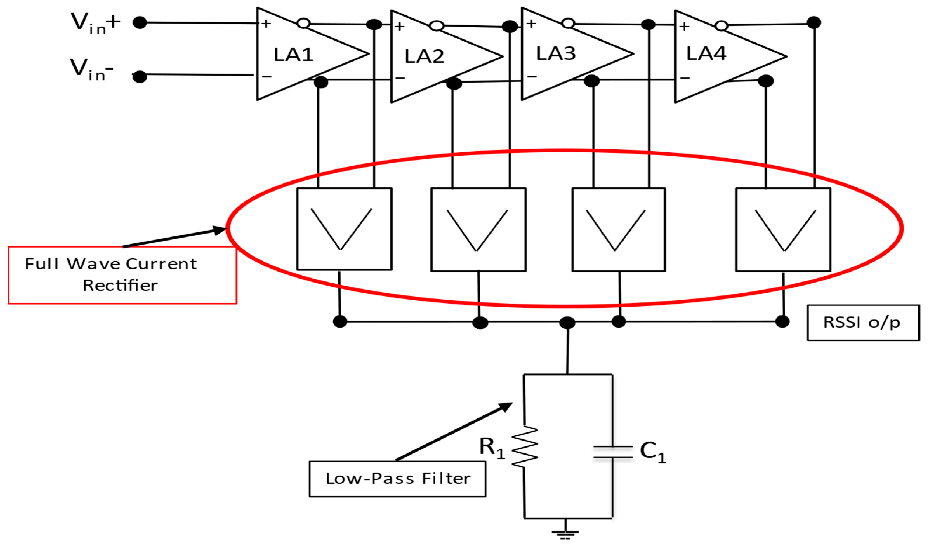
2. RSSI System
3. RSSI Circuits
4. Simulation Results and Analysis
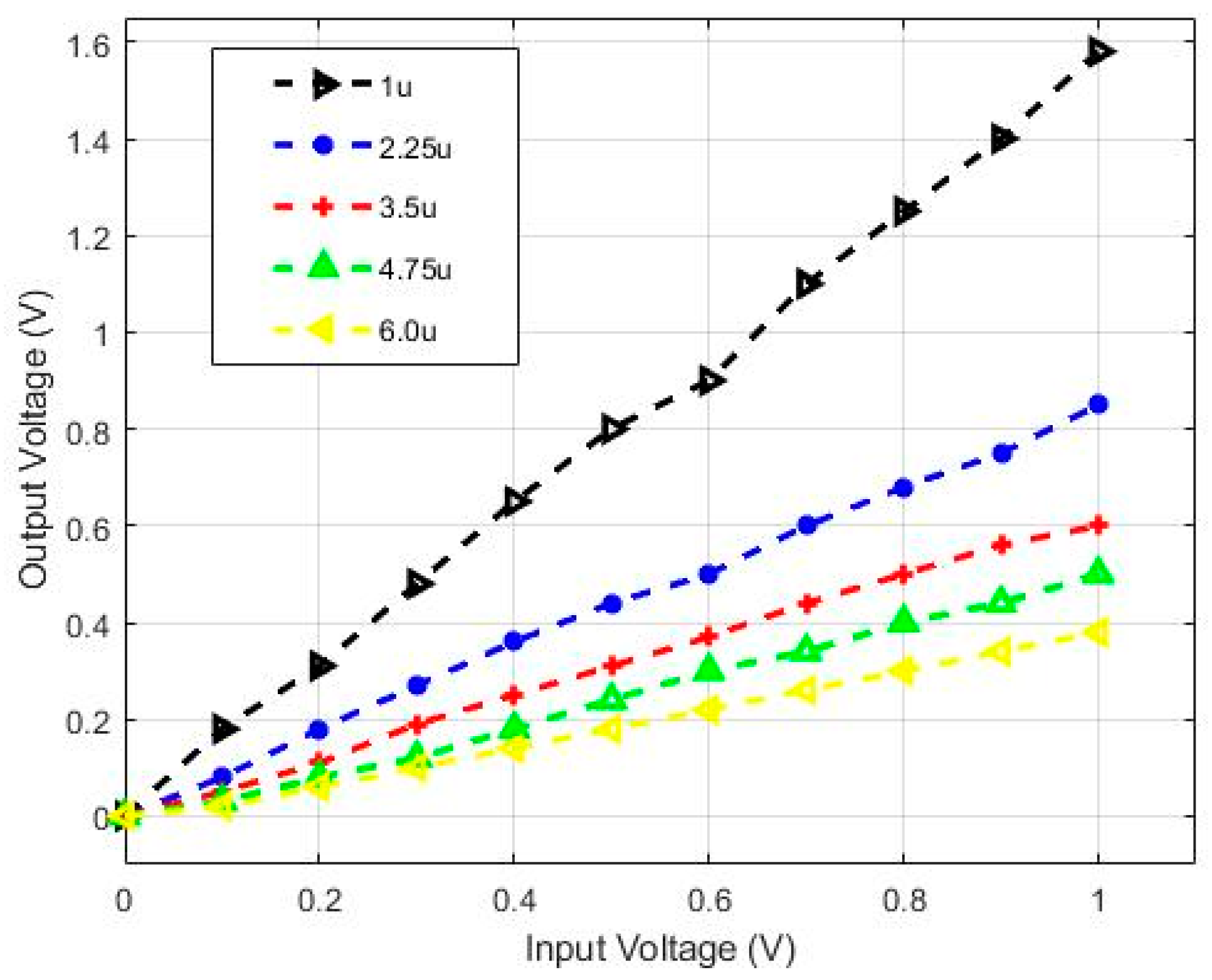
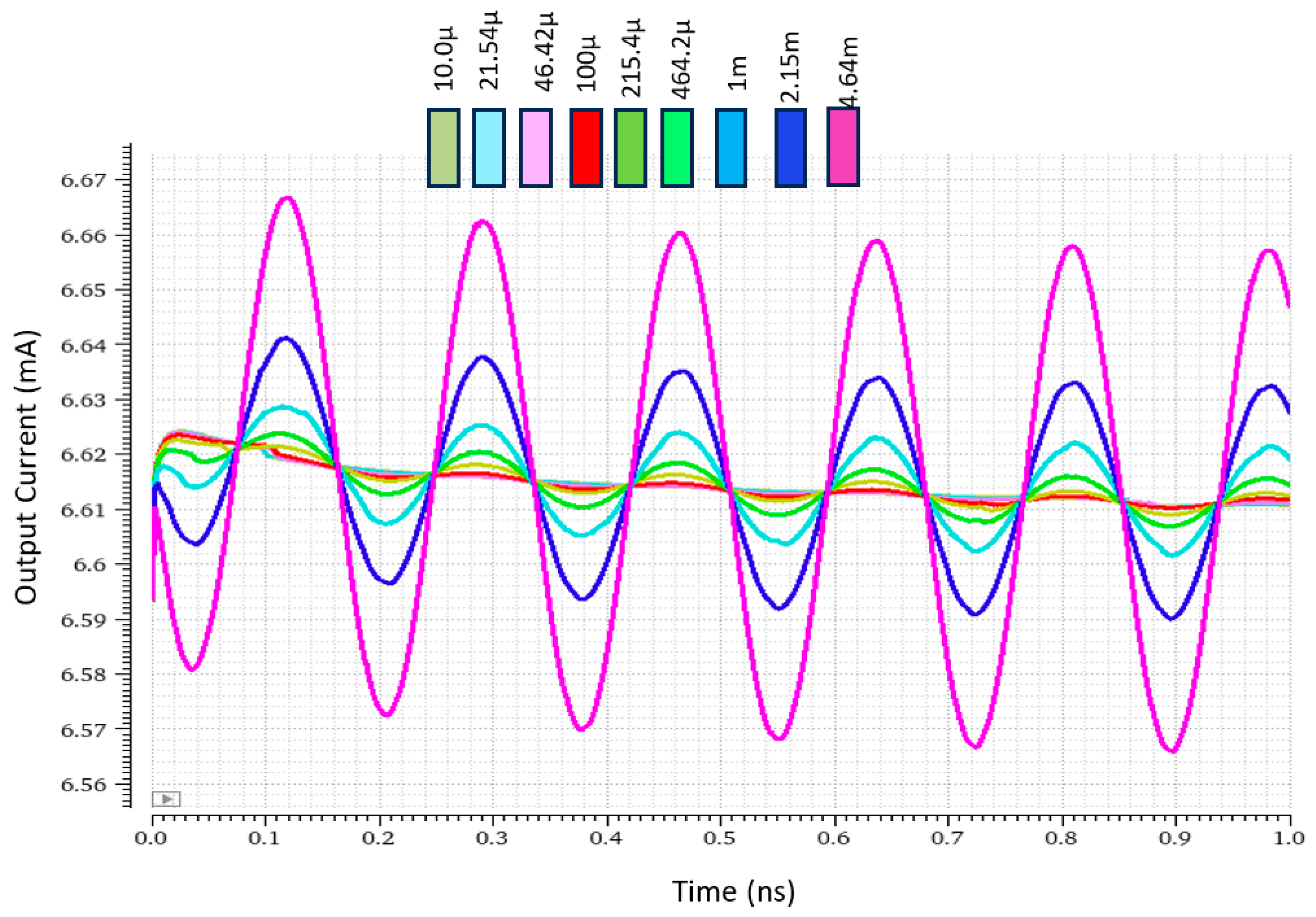
4.1. Limiting Cell
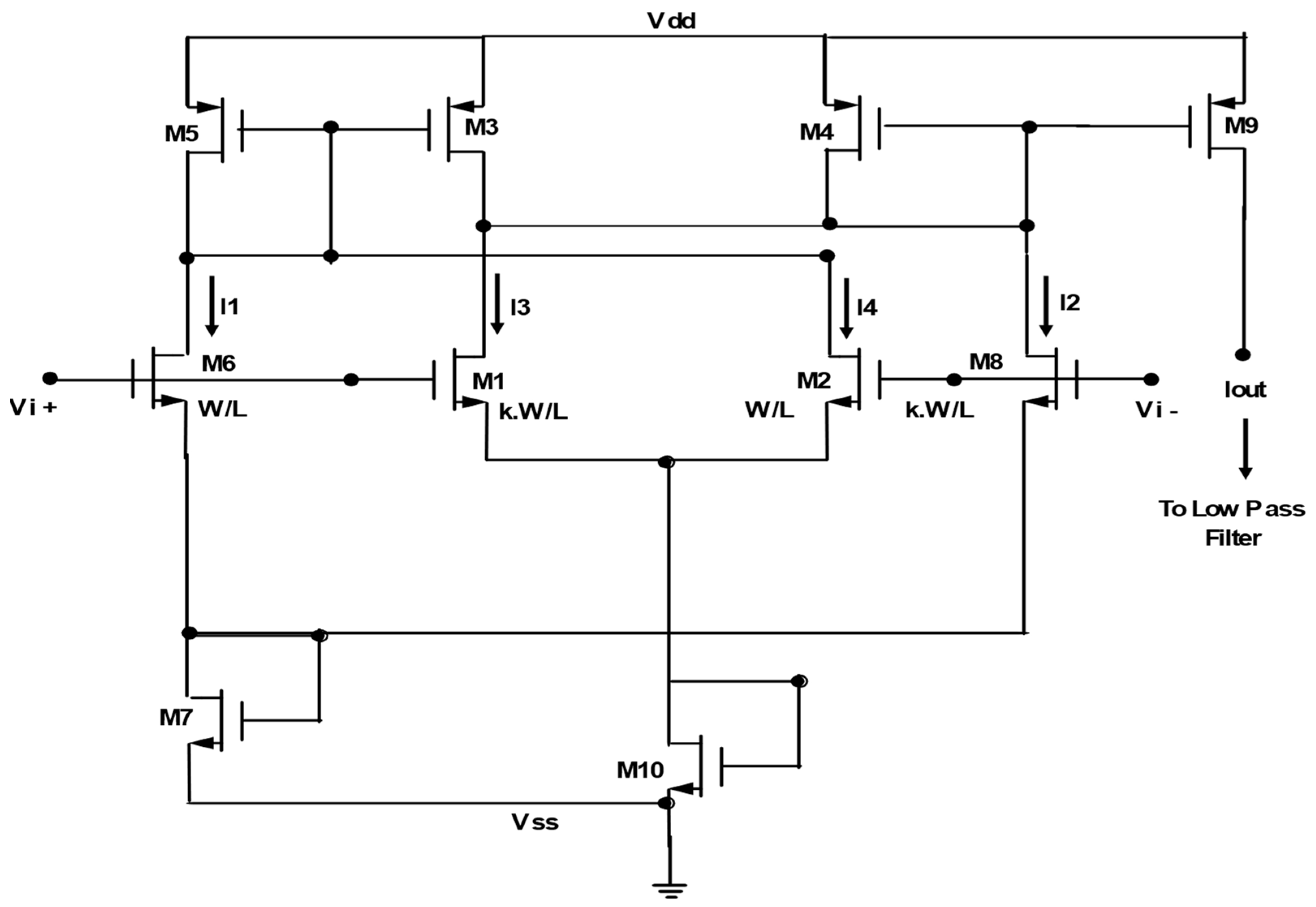
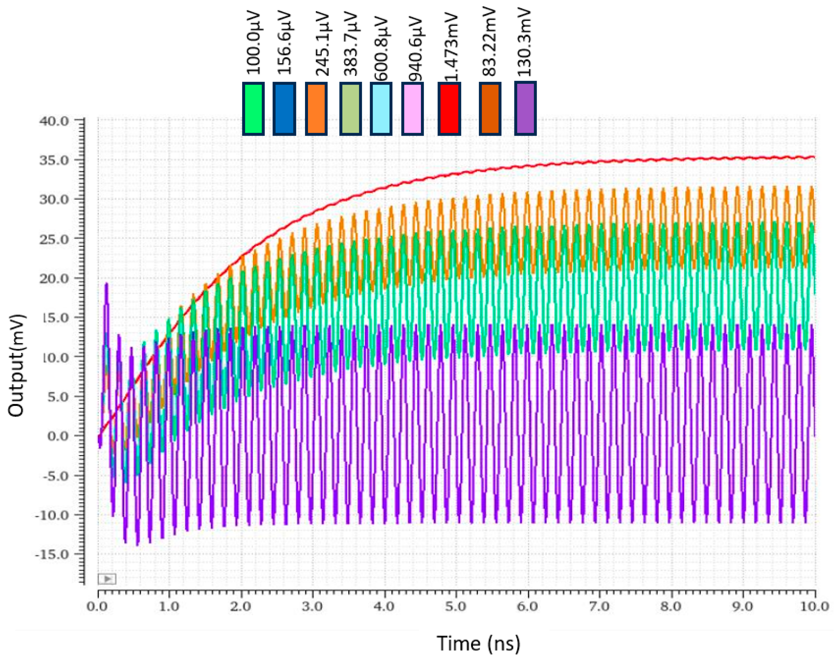
4.2. Full-Wave Current Rectifier
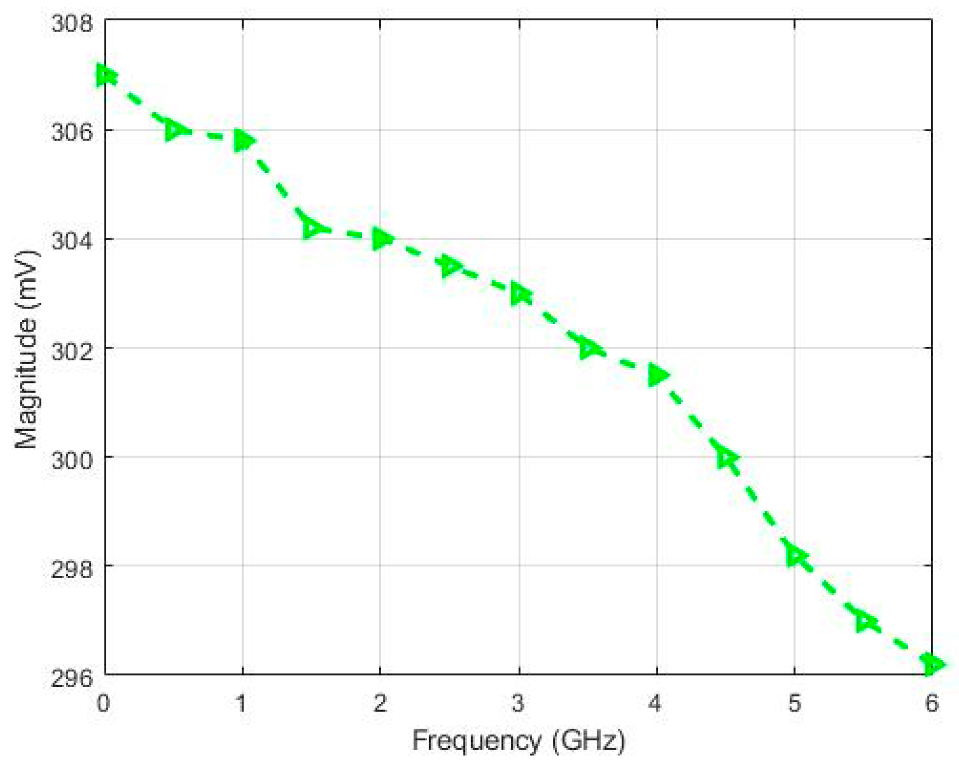
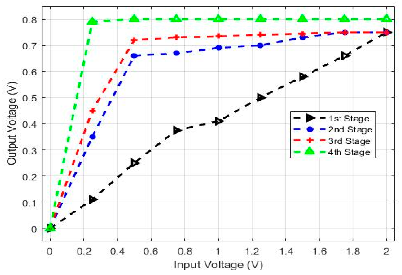
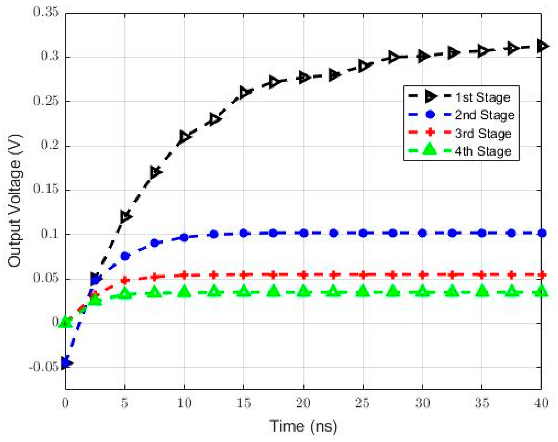
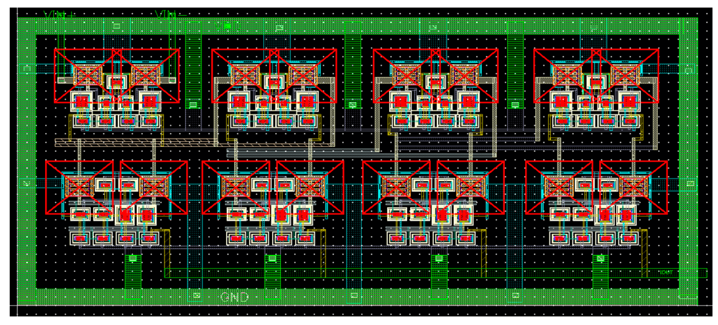
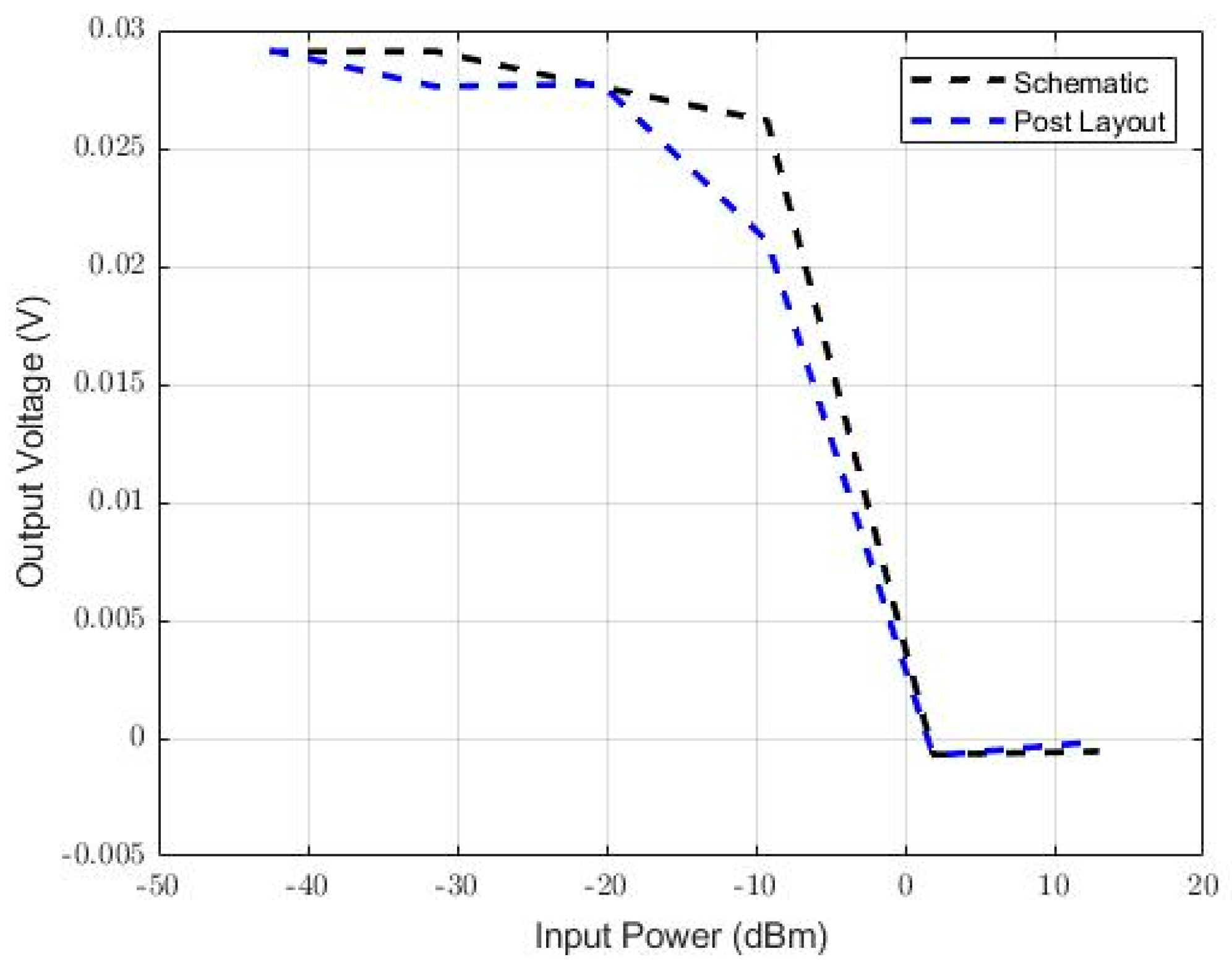
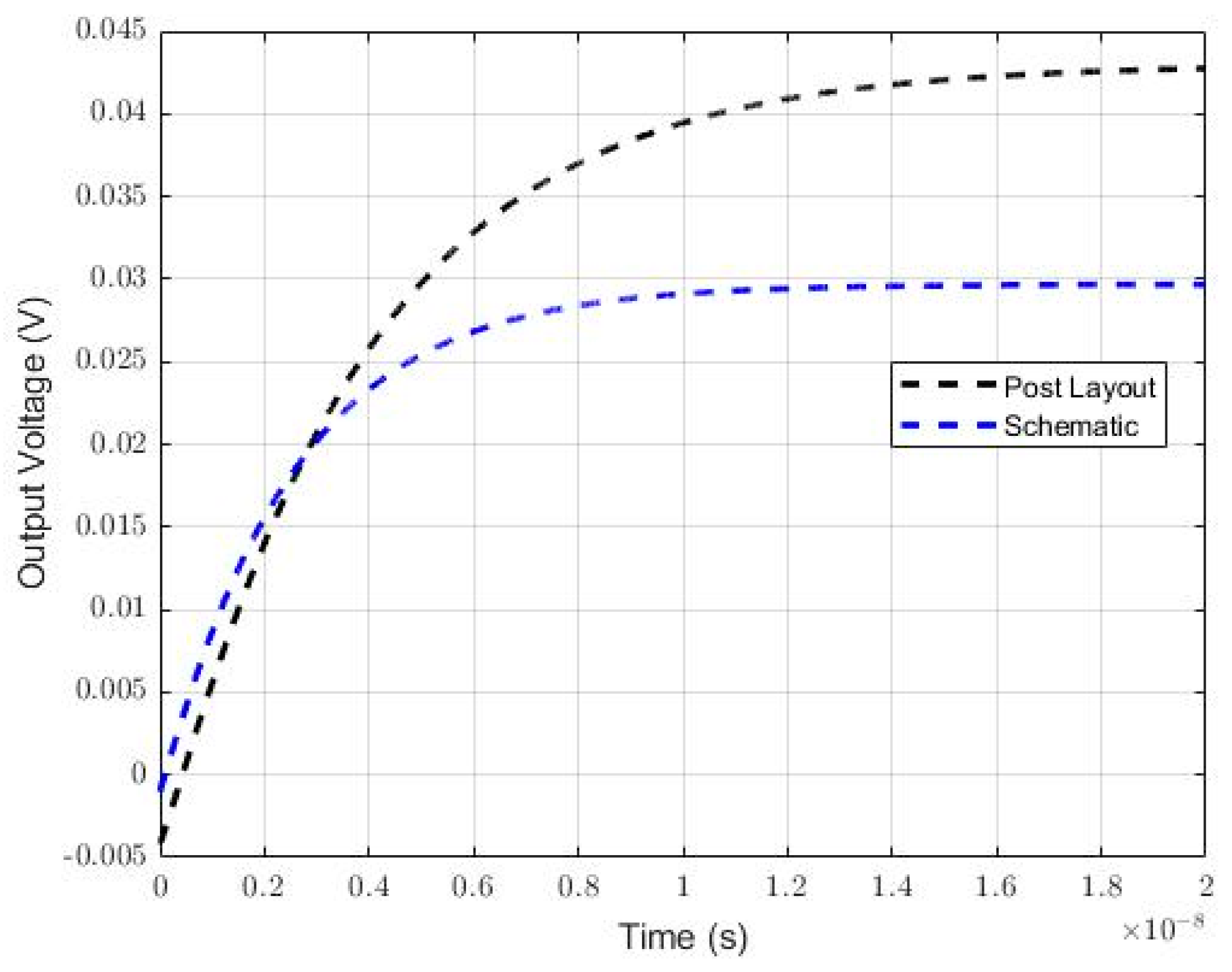
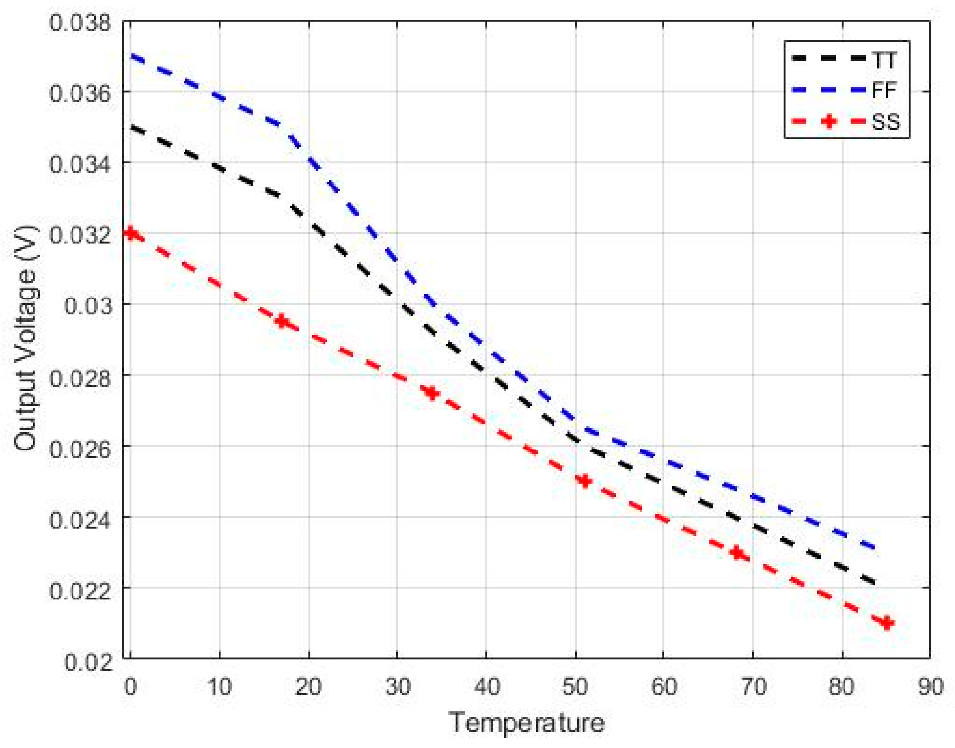
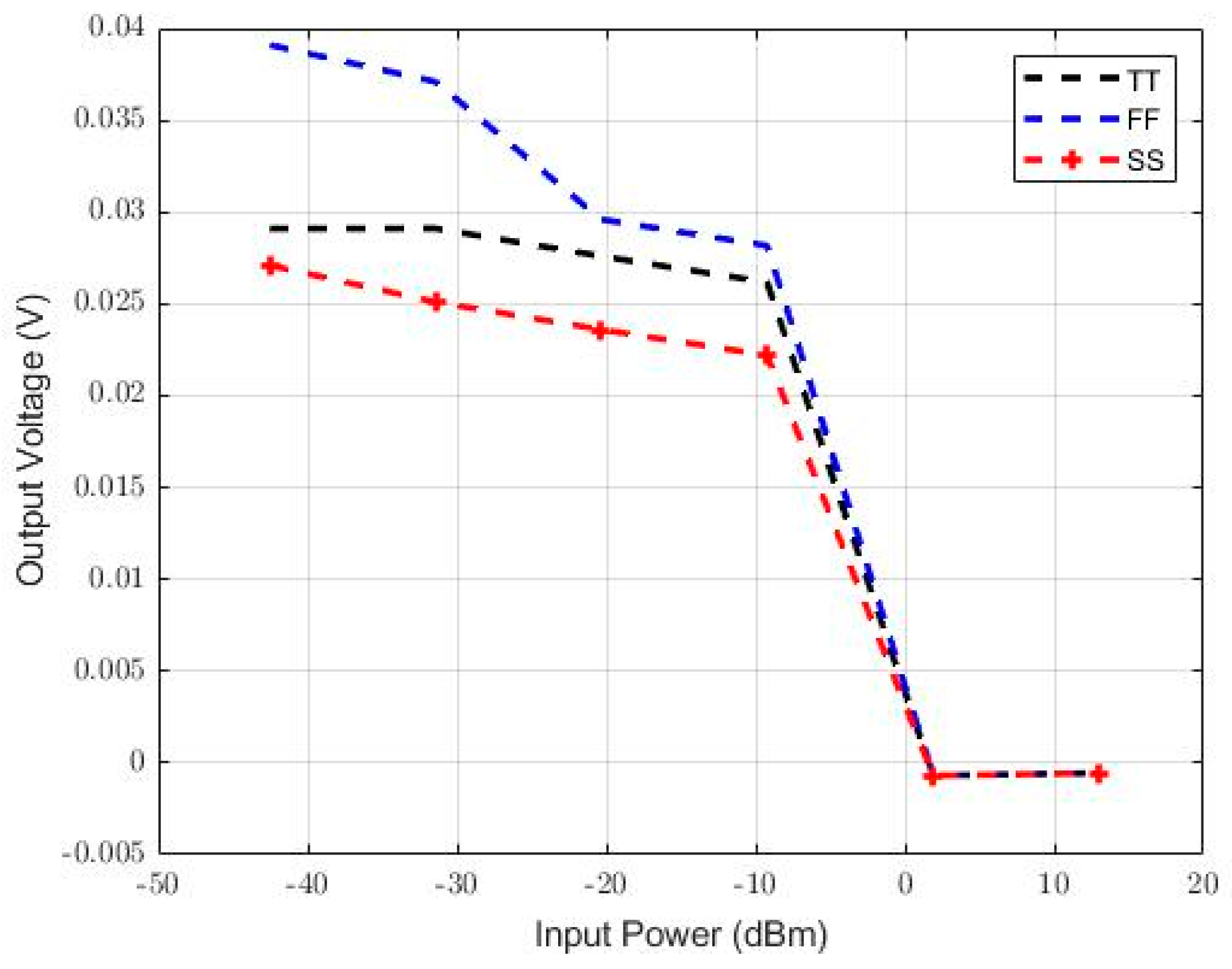
4.3. RSSI Circuit
5. Conclusions and Future Work
Author Contributions
Funding
Data Availability Statement
Acknowledgments
Conflicts of Interest
References
- Wireless Charging: The Way of the Future and Some of the Reasons Why. Powermat. 2022. Available online: https://powermat.com/blog/wireless-charging-the-way-of-the-future-and-some-of-the-reasons-why/ (accessed on 26 September 2023).
- Lu, X.; Wang, P.; Niyato, D.; Kim, D.; Han, Z. Wireless Charging Technologies: Fundamentals, Standards, and Network Applications. IEEE Commun. Surv. Tutor. 2016, 18, 1413–1452. [Google Scholar] [CrossRef]
- Jawad, A.M.; Jawad, H.M.; Nordin, R.; Gharghan, S.K.; Abdullah, N.F.; Abu-Alshaeer, M.J. Wireless Power Transfer with Magnetic Resonator Coupling and Sleep/Active Strategy for a Drone Charging Station in Smart Agriculture. IEEE Access 2019, 7, 139839–139851. [Google Scholar] [CrossRef]
- Fu, X.; Wang, Y.; Li, W.; Yang, Y.; Postolache, O. Lightweight Fault Detection Strategy for Wireless Sensor Networks Based on Trend Correlation. IEEE Access 2021, 9, 9073–9083. [Google Scholar] [CrossRef]
- Khan, M.A.; Quresh, I.M.; Khanzada, F. A Hybrid Communication Scheme for Efficient and Low-Cost Deployment of Future Flying Ad-Hoc Network (FANET). Drones 2019, 3, 16. [Google Scholar] [CrossRef]
- Zhang, M.; Liu, R.; Zhang, Y.; Wang, W.; Liu, H.; Lu, C. A fully integrated RSSI and an ultra-low power SAR ADC for 5.8 GHz DSRC ETC transceiver. AEU-Int. J. Electron. Commun. 2018, 86, 154–163. [Google Scholar] [CrossRef]
- Chibi, N.; Ghazi, H.; Fihri, W. Drone Cyber-Attack: An Intrusion Detection Technique Based on RSSI and Trilateration. In Proceedings of the 2021 Third International Conference on Transportation and Smart Technologies (TST), Tangier, Morocco, 27–28 May 2021; pp. 42–45. [Google Scholar] [CrossRef]
- Byun, S. Analysis and Design of CMOS Received Signal Strength Indicator. IEEE Trans. Circuits Syst. I 2014, 61, 2970–2977. [Google Scholar] [CrossRef]
- Zhang, X.; Chi, B.; Liu, B.; Wang, Z. −80dBm~0dBm dynamic range, 30mV/dB detection sensitivity piecewise RSSI for SDR/CR receivers. In Proceedings of the 2014 IEEE 57th International Midwest Symposium on Circuits and Systems (MWSCAS), College Station, TX, USA, 3–6 August 2014; pp. 89–92. [Google Scholar] [CrossRef]
- Lei, Q.; Lin, M.; Peng, M.; Chen, Z.; Shi, Y. A CMOS low power, wide dynamic range RSSI with integrated AGC loop. In Proceedings of the 2011 IEEE International Conference on Anti-Counterfeiting, Security and Identification, Xiamen, China, 24–26 June 2011; pp. 173–176. [Google Scholar] [CrossRef]
- Kim, H.-S.; Ismail, M.; Olsson, H. CMOS limiters with RSSIs for Bluetooth receivers. In Proceedings of the 44th IEEE 2001 Midwest Symposium on Circuits and Systems, MWSCAS 2001 (Cat. No.01CH37257), Dayton, OH, USA, 14–17 August 2001; Volume 2, pp. 812–815. [Google Scholar] [CrossRef]
- Huang, P.; Chen, Y.; Wang, C. A 2-V 10.7-MHz CMOS limiting amplifier/RSSI. IEEE J. Solid-State Circuits 2000, 35, 1474–1480. [Google Scholar] [CrossRef]
- The, Y.J.; Choi, Y.B.; Yeoh, W.G. A 40-MHz CMOS RSSI with data slicer. In Proceedings of the 2007 International Symposium on Integrated Circuits—ISIC, Singapore, 26–28 September 2007; pp. 385–388. [Google Scholar]
- AlSuwaidi, M.; Albasha, L.; Mir, H. A Frequency Synthesizer for Wireless Power Transfer at 5.8 GHz and 61 GHz. In Proceedings of the 2022 Advances in Science and Engineering Technology International Conference, Dubai, United Arab Emirates, 21–24 February 2022. [Google Scholar]
- Iqbal, U.; Albasha, L.; Mir, H. A Transmitter Antenna Array System for Wireless Power Transfer at 5.8 GHz. In Proceedings of the 2022 Advances in Science and Engineering Technology International Conference, Dubai, United Arab Emirates, 21–24 February 2022. [Google Scholar]
- Pahlavan, S.; Shooshtari, M.; Maleki, M.; Jafarabadi Ashtiani, S. Using Overlapped Resonators in Wireless Power Transfer for Uniform Electromagnetic Field and Removing Blank Spots in Free Moving Applications. Electronics 2022, 11, 1204. [Google Scholar] [CrossRef]
- Pahlavan, S.; Ashtiani, S.J. Rotation-Tolerant Wireless Power Transmission Scheme with Smart Positioning for Cognitive Research on Moving Animals. IEEE Trans. Biomed. Circuits Systems 2023, 1–8. [Google Scholar] [CrossRef] [PubMed]
- Shin, J.; Bae, J.; Koo, H.; Bae, S.; Na, J.; Oh, H.; Jeon, H.; Jung, H.; Choi, Y.C.; Woo, S.; et al. 5.8 GHz 4-Channel Beamforming Tx IC for Microwave Power Transfer. IEEE Access 2021, 9, 72316–72325. [Google Scholar] [CrossRef]
- Ming-Bo, L. Introduction to VLSI Systems: A Logic, Circuit, and System Perspective; CRC Press: Boca Raton, FL, USA, 2011. [Google Scholar]
- Dehghani, R. Design of CMOS Operational Amplifiers; Artech House: Norwood, MA, USA, 2013. [Google Scholar]
- Kitsunezuka, M.; Kodama, H.; Oshima, N.; Kunihiro, K.; Maeda, T.; Fukaishi, M. A 30 MHz–2.4 GHz CMOS receiver with integrated RF filter and dynamic-range-scalable energy detector for cognitive radio. In Proceedings of the 2011 IEEE Radio Frequency Integrated Circuits Symposium, Baltimore, MD, USA, 5–7 June 2011; pp. 1–4. [Google Scholar] [CrossRef]
- Fu, X.; Wang, Y.; Yang, Y.; Postolache, O. Analysis on cascading reliability of edge-assisted Internet of Things. Reliab. Eng. Syst. Saf. 2022, 223, 108463. [Google Scholar] [CrossRef]
- Fu, X.; Li, Q.; Li, W. Modeling and analysis of industrial IoT reliability to cascade failures: An information-service coupling perspective. Reliab. Eng. Syst. Saf. 2023, 239, 109517. [Google Scholar] [CrossRef]


| Specification | Value |
|---|---|
| Supply voltage | 1 V |
| Frequency | 5.8 GHz |
| Power | <30 Mw |
| Sensitivity level | <0.3 Mv |
| Dynamic range | 50 Db |
| Technology | 65 nm |
| [9] Simulated | [10] Measured | [12] Measured | [13] Measured | [21] Measured | This Work: Simulated | |
|---|---|---|---|---|---|---|
| Frequency | 0.1–20 MHz | 0.3–17 MHz | 10.7 MHz | 40 MHz | 0.03–2.4 GHz | 5.8 GHz |
| Dynamic Range | 80 dB | 56 dB | 75 dB | 56 dB | 29–48 dB | 34 dB |
| Power (mW) | 1.2–2.9 | 1.8 | 6.2 | 9 | 30–44 | 2 |
| Area (mm2) | 0.06 | 0.16 | 0.4 | 0.05 | - | 0.008 |
| Logarithmic Error | 1.4 dB | 0.5 dB | 1 dB | 1 dB | - | 0.4 dB |
| Sensitivity Level | 30 mV/dBm | - | 10 mV/dBm | - | 13 mV/dBm | 17 mV/dBm |
| Technology | 65 nm | 130 nm | 0.6 um | 130 nm | 90 nm | 65 nm |
Disclaimer/Publisher’s Note: The statements, opinions and data contained in all publications are solely those of the individual author(s) and contributor(s) and not of MDPI and/or the editor(s). MDPI and/or the editor(s) disclaim responsibility for any injury to people or property resulting from any ideas, methods, instructions or products referred to in the content. |
© 2023 by the authors. Licensee MDPI, Basel, Switzerland. This article is an open access article distributed under the terms and conditions of the Creative Commons Attribution (CC BY) license (https://creativecommons.org/licenses/by/4.0/).
Share and Cite
Quadir, N.; Alawar, F.S.; Albasha, L.; Mir, H. Linear-in-dB Logarithmic Signal Strength Sensor Circuit for Wireless Power Transfer Receivers. Energies 2023, 16, 7612. https://doi.org/10.3390/en16227612
Quadir N, Alawar FS, Albasha L, Mir H. Linear-in-dB Logarithmic Signal Strength Sensor Circuit for Wireless Power Transfer Receivers. Energies. 2023; 16(22):7612. https://doi.org/10.3390/en16227612
Chicago/Turabian StyleQuadir, Nasir, Fatma S. Alawar, Lutfi Albasha, and Hasan Mir. 2023. "Linear-in-dB Logarithmic Signal Strength Sensor Circuit for Wireless Power Transfer Receivers" Energies 16, no. 22: 7612. https://doi.org/10.3390/en16227612
APA StyleQuadir, N., Alawar, F. S., Albasha, L., & Mir, H. (2023). Linear-in-dB Logarithmic Signal Strength Sensor Circuit for Wireless Power Transfer Receivers. Energies, 16(22), 7612. https://doi.org/10.3390/en16227612