1. Introduction
Benefiting from the rapid development of energy management technologies, battery energy storage systems (BESS), as one of the vital components, have gained extensive applications. They are typically constructed by connecting low-voltage, high-capacity cells in series [
1,
2,
3,
4]. Due to factors such as manufacturing processes and operating temperatures, discrepancies in the state of charge (SOC) of individual cells among battery packs within a series-connected structure are common, imposing limitations on the performance and functionality of the BESS [
5,
6,
7]. CLLC resonant converters, as one of the high-performance and wide-range bidirectional DC/DC topologies [
8], are well suited for applications in battery balancing to enhance the performance of BESS.
Figure 1 illustrates the typical topology of a CLLC resonant converter, which can be functionally simplified into three main units: the chopper unit, the resonator unit, and the rectifier unit, denoted by green, gray, and blue color blocks, respectively. Influenced by the voltage fluctuations in individual cells under various operational conditions, the converter has to achieve both high energy transfer efficiency with heavy load conditions and cell balancing among packs with light load conditions. With a heavy load, the converter applies pulse frequency modulation (PFM) to adjust the switching frequency to be lower than the resonant frequency, which causes the converter to operate in the under-resonant mode to achieve a high voltage gain. In this mode, the CLLC resonant converter can attain zero voltage switching (ZVS) for the switch devices in the chopping unit, ensuring efficient operation [
9,
10]. Similarly, under light load conditions, the converter applies PFM to adjust the operating frequency to be higher than the resonant frequency, which enables the converter to function in the over-resonant mode to achieve a low voltage gain [
11,
12]. This mode ensures ZVS for the switch devices in the chopping unit and zero current switching (ZCS) for the switch devices in the rectification unit of the converter. However, as the load decreases even further, reducing the voltage gain with PFM becomes challenging due to the extremely high switching frequencies, requiring a high-performance digital controller. To address this issue, researchers have proposed a hybrid modulation mode that seamlessly combines PFM and phase-shift modulation (PSM) [
13,
14,
15]. In most cases, the CLLC resonant converter applies PFM to either increase or decrease the switching frequency of the chopping unit to achieve output gain adjustment. Once it is unable to reach the desired output voltage requirement even at the highest switching frequency, the hybrid modulation algorithm helps the converter to transition from PFM to PSM as soon as possible. With PSM, the converter regulates the phase-shift angle to control the RMS output voltage of the chopping unit, which is applied as the input of the resonant tank. Moreover, J.Y. et al. proposed a synchronous rectification method for the case in which the converter is in PSM mode [
16,
17,
18]. Moreover, T. et al. discussed the losses that may occur during PFM and PSM in CLLC resonant converters [
19,
20]. Although these analyses are informative, the detailed design of modulation mode transition has not been thoroughly explored and revealed.
To optimize the hybrid modulation strategy of CLLC resonant converters, this paper introduces a dynamic transition algorithm aimed at reducing the likelihood of repetitive and unnecessary modulation mode changes caused by noise at critical states. Compared to traditional hybrid modulation, the proposed algorithm manages the transition process more precisely due to adaptive updates of the controller parameters. Furthermore, building upon the traditional approach, it employs error analysis and hysteresis control under the current switch frequency and phase-shift angle to prevent undesired modulation mode changes. Finally, a 1 kW prototype CLLC circuit is utilized in experiments to verify the performance and feasibility of the proposed algorithm.
2. Analysis of Hybrid Modulation
In the buck mode of a full-bridge CLLC resonant converter, the hybrid modulation strategy encompasses two fundamental modulation techniques: PFM and PSM.
In this section, a comparative analysis of the two fundamental modulation methods is conducted concerning system gain analysis and control loop design. Concerning system gain analysis, the focus will be on considering the components contributing to the gain of the CLLC resonant converter and deriving quantitative expressions for each modulation method using an efficient simplified analysis approach. As for control loop design, the approach will involve utilizing computer simulation techniques to obtain the open-loop dynamic characteristics of CLLC resonant converters, thereby providing valuable guidance for the design of the PI compensator. Based on the two points mentioned above, a comprehensive hybrid modulation strategy with the traditional mode selector algorithm is constructed.
2.1. Gain Analysis of Modulations
The system gain of CLLC resonant converters is the cumulative result of three gains, each determined by the chopping unit, the resonant tank unit, and the rectifier unit, respectively.
As the input part of the CLLC resonant converter, the chopping unit converts the DC voltage into AC voltage with distinct characteristics, which are influenced by the various modulation techniques. As illustrated by the red curve in
Figure 2a, when the CLLC resonant converter is modulated with PFM, this unit generates a square wave signal with a
duty cycle and the same amplitude but varying periods. However, when the converter is modulated with PSM, this unit generates a square wave signal with the same amplitude and the same periods but varying duty cycles, which is depicted by the red curve in
Figure 2b.
The resonant tank unit is one of the most critical parts in the converter. Within the resonant tank unit, the combined interaction of five resonant components results in entirely distinct output voltages for varying duty cycles and frequencies of input signals, which are determined by the chopping unit. In general, there are two classical methods for the analysis of the effects of the input signals: the time domain analysis method (TDA) and the fundamental harmonic approximation method (FHA) [
19,
21,
22]. Compared to TDA, the most significant advantage of FHA is its lower computational complexity and higher accuracy. Thanks to these advantages, FHA has become the preferred choice for the analysis of resonant tanks in engineering applications. It focuses solely on the impact of the fundamental harmonic on the energy transfer process and simplifies the transfer function using impedance analysis techniques [
23,
24,
25].
The foundation of FHA is Fourier expansion, which can be expressed as
where
,
, and
.
The blue sinusoidal curve in
Figure 2 illustrates the first harmonic waveform corresponding to different modulation modes. In the PFM modulation mode, an equivalent input waveform can be obtained as in Equation (
2)
where
and
is the input bus voltage.
Similarly, in the PSM modulation mode, an equivalent input waveform can be obtained as in Equation (
4)
where
The amplitude and phase angle of the fundamental harmonics modulated by PFM and PSM can be obtained by referring to Equations (
2) and (
4), respectively. It is important to note that the phase angle does not affect the gain variation of the resonant tank. Thus, the only factor that affects the operation of the resonant tank is the amplitude of the fundamental harmonic, which can also be considered as the effective value of the fundamental harmonic. When PFM and PSM operate at the same switching frequency, the normalized expression for the input of the resonant tank can be simplified as in:
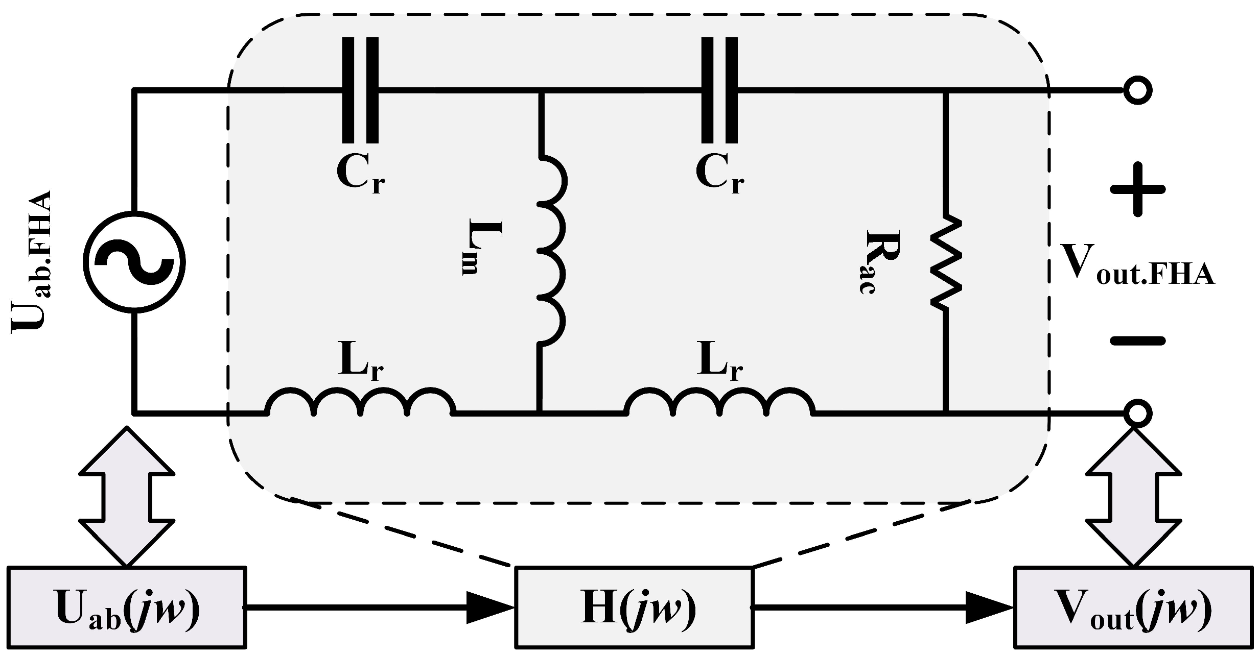
Figure 3 illustrates the simplified model of a symmetric CLLC resonant tank unit. The analysis of this simplified model in the frequency domain leads to the derivation of the transfer function of the resonant tank unit under fundamental excitation, which can be expressed as in:
where
, and
.
Taking the magnitude of Equation (
10) and simplifying it yields the normalized expression for the resonant tank gain, which can be obtained as in
where
is the quality factor,
is the inductor ratio,
is the normalized frequency ratio,
is the switch frequency, and
) is the quasi-resonant frequency.
The rectification unit, being a fixed structure (full-bridge rectification) after the resonant tank unit, is not influenced by the modulation strategy of the chopping unit. Consequently, its normalized gain can be considered as
[
26].
By integrating the analysis of Equations (
9) and (
11), the normalized system gain of CLLC resonant converters can be expressed as in
Based on Equation (
12), the normalized gain curves of the CLLC resonant converter can be visualized under different load conditions, as illustrated in
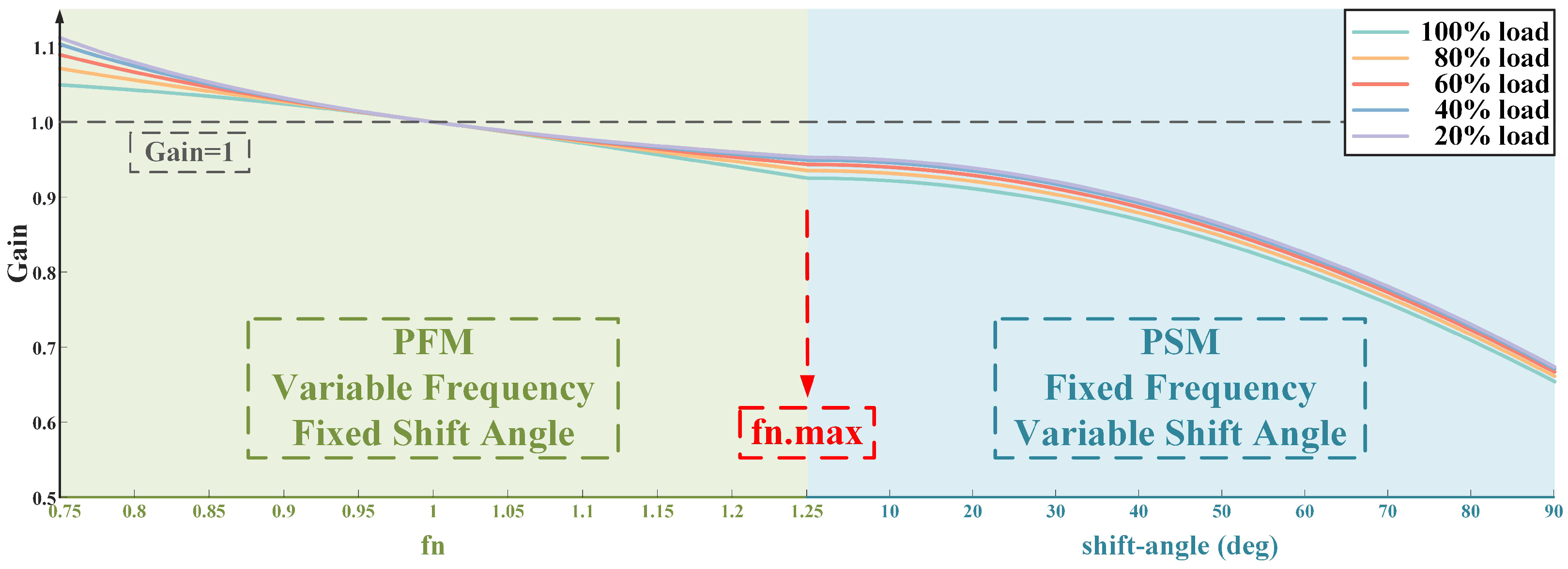
Figure 4. The left half of
Figure 4 exhibits the converter operating in PFM modulation mode: when
, the gain curve exhibits pronounced changes; meanwhile, when
, the gain curve tends to change more smoothly, and it almost loses its regulation capability. The right part of
Figure 4 depicts the converter operating in the PSM modulation mode with the maximum switch frequency: as the phase-shift angle increases, compared to the PFM modulation mode with the same switch frequency, the converter’s gain significantly decreases. Therefore, the hybrid modulation mode combining PFM and PSM can effectively broaden the operating range of the converter and improve its efficiency.
2.2. Design of the Control Loop
In practical power converter systems, noise caused by the parasitic parameters of devices occurs frequently, and the consequences can range from significant power supply output ripples to more severe effects such as output voltage oscillations and damage to power components. To address the mentioned issues, it is necessary to introduce an appropriate compensator in the system feedback loop to regulate the power converter’s performance in the presence of disturbances. A well-designed compensator can ensure the stability of the converter and improve its dynamic response characteristics.
The stability of a control loop is specifically depicted on a Bode plot through the parameters known as the phase margin (PM) and gain margin (GM). PM is defined as the difference between the phase angle at the system’s crossover frequency and −
. Typically, engineers set PM to be greater than
based on their experience, striking a balance between system damping and transient response capability. GM, on the other hand, is defined as the difference between the gain at the phase angle of −
and 0 dB. It is generally required to be greater than 6 dB for system stability. When the cumulative impact of the compensator and power converter displays adequate PM and GM on the Bode plot, it indicates that the compensator can enhance the performance of the converter [
27,
28].
The proportional-integral (PI) controller is one of the most commonly used compensators [
29,
30], and its transfer function is typically represented as in Equation (
13)
where
is the proportional coefficient, and
is the integral coefficient.
Based on Equation (
13), one can deduce the gain expression,
and phase expression,
for the compensator.
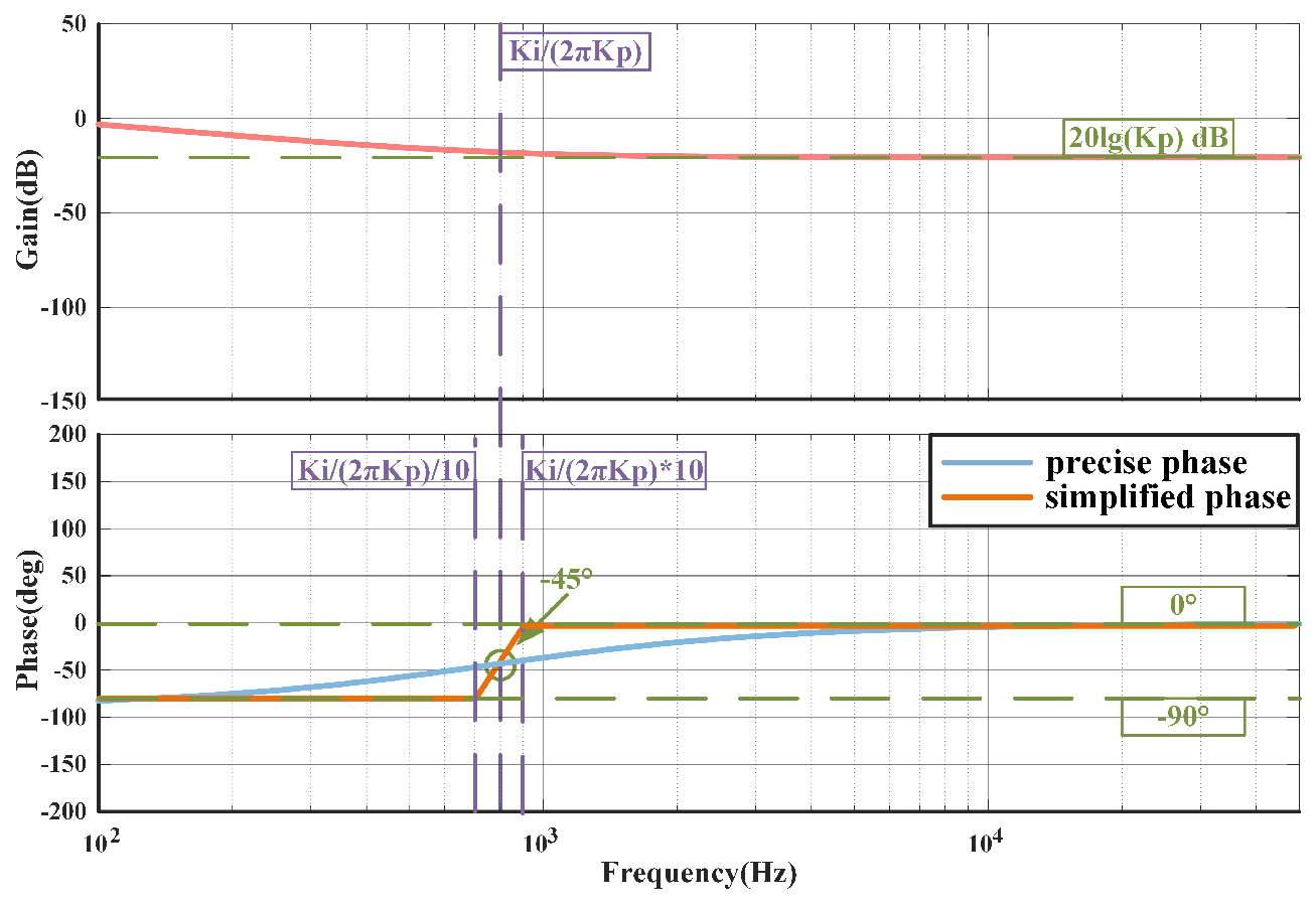
The gain and phase characteristics of the PI compensator are both depicted in
Figure 5. The trend of the gain curve is primarily decided by the ZERO. When the frequency is lower than
Hz, the curve follows an approximate −20 dB/decade slope; however, when the frequency exceeds
Hz, the interaction between the pole and zero gradually brings the gain curve closer to 0 dB. Similarly, the trend of the phase curve is influenced by the ZERO. As the frequency approaches 0 Hz, the phase lags by
; when the frequency equals
Hz, the phase exhibits a lag of
; and as the frequency tends towards infinity, the interaction between the ZERO and POLE causes the phase to approach
. To avoid complex nonlinear computations, the design of the PI is simplified by approximating the curves with linearization. Therefore, once the crossover frequency is selected, the calculation of constraint equations can be carried out based on the gain and phase of the power converter. With the adjustment of the PI compensator, when
, the open-loop gain is compensated to reach 1. Similarly, compared to the original phase without the compensator, the open-loop phase is increased by
when
. Combining the discussion above and the simplified analysis in
Figure 5, the constraint equations can be expressed as in
where
is the selected crossover frequency, and
represents the gain of the open-loop system analyzed using the small signal model and computer simulations.
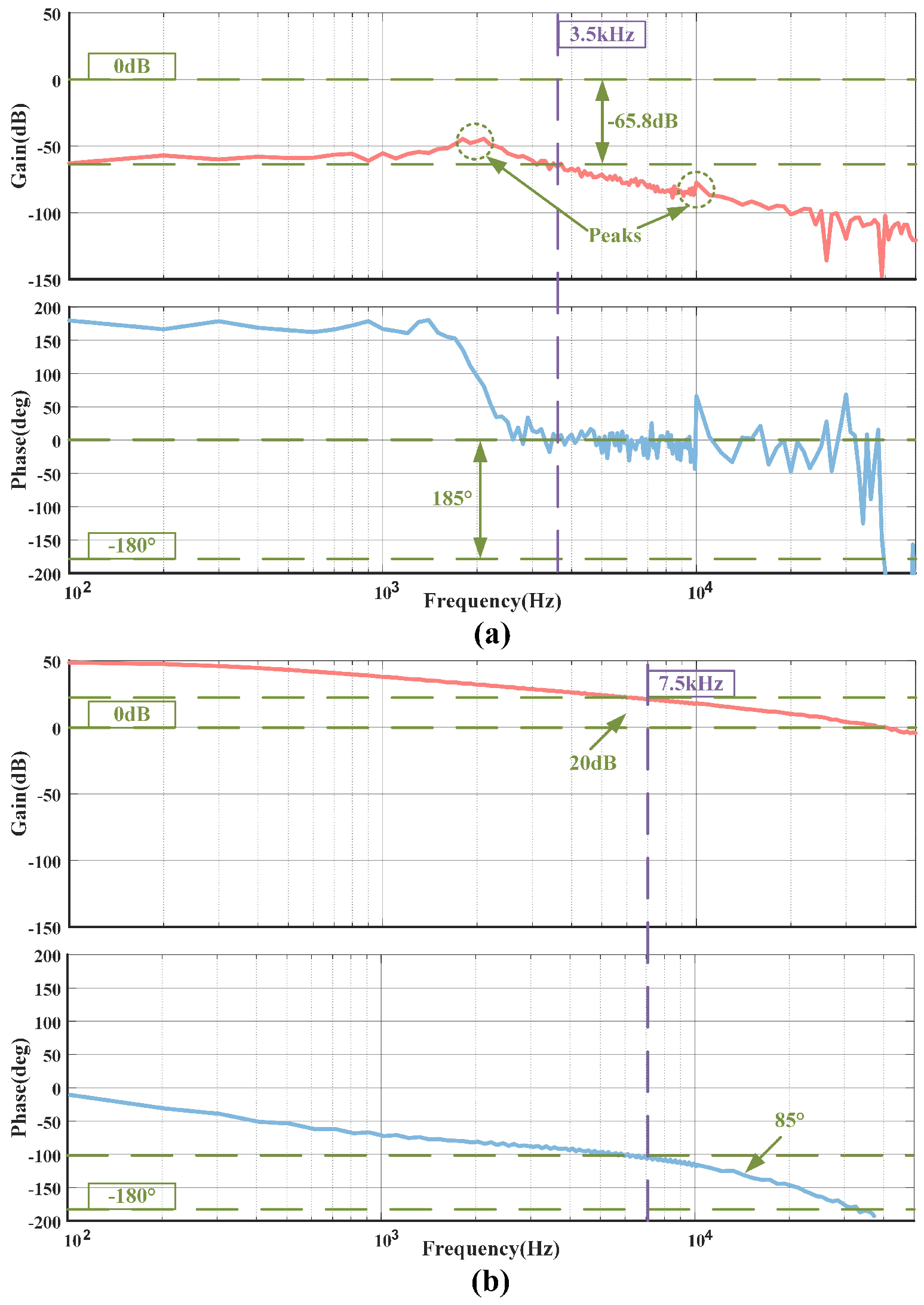
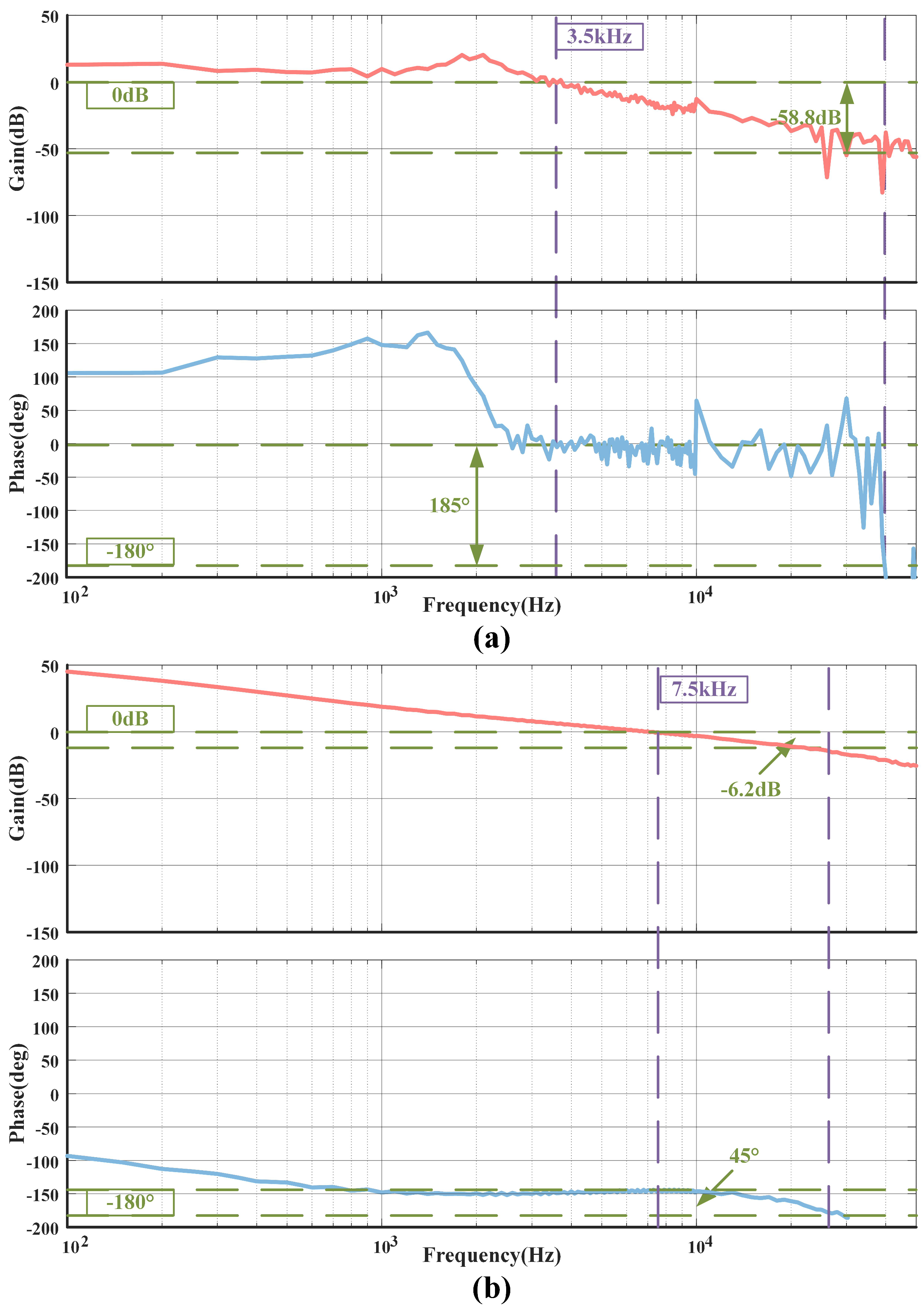
By utilizing computer simulation techniques, the loop characteristics of the CLLC resonant converter can be easily obtained. The Bode plot in
Figure 6 displays the open-loop characteristic curve of the converter when it operates in PFM mode, which shows a significantly low gain at low frequencies. Additionally, due to the complex structure of the resonant tank, there are two resonance peaks located near
kHz and
kHz, making compensator bandwidth design challenging. Fortunately, the phase curve presents a favorable trend, indicating that the system’s PM will not be affected by the phase lag of the compensator. To meet the dynamic performance requirements, a relatively conservative crossover frequency of
kHz has been set, which provides a gain of −
dB and a phase angle of
, making it ideal for compensation.
On the other hand, when the converter operates using the PSM modulation method, its open-loop characteristic curve has a high bandwidth gain curve of approximately 40 kHz, as shown in
Figure 6b. However, the phase curve’s trend is non-ideal, which poses a significant constraint on compensator design. To ensure the stable operation of the converter, the PM with compensation should be at least
, indicating that the original PM should be selected in the range of
to
. To meet the dynamic performance requirements and considering the above analysis, a conservative crossover frequency of
kHz has been set. At this frequency, the original open-loop characteristic curve has a gain of 20 dB and a phase of −
, providing ample room for compensation.
By substituting the chosen crossover frequency into Equation (
16), the corresponding compensator parameters can be obtained by solving the equation set. The solutions of the equation set for PFM mode are
and
, while the solutions for PSM mode are
and
.
Figure 7 shows the loop characteristics of the CLLC resonant converter under the influence of the PI compensator. When the converter operates using the PFM modulation method, the GM is
dB, and the PM is
, ensuring the stable operation of the CLLC resonant converter under PFM mode based on engineering experience. Similarly, when the converter operates using the PSM modulation method, the GM is
dB, and the PM is
, demonstrating its outstanding system stability and exceptional system dynamic characteristics.
2.3. Introduction of the Traditional Mode Selector Method
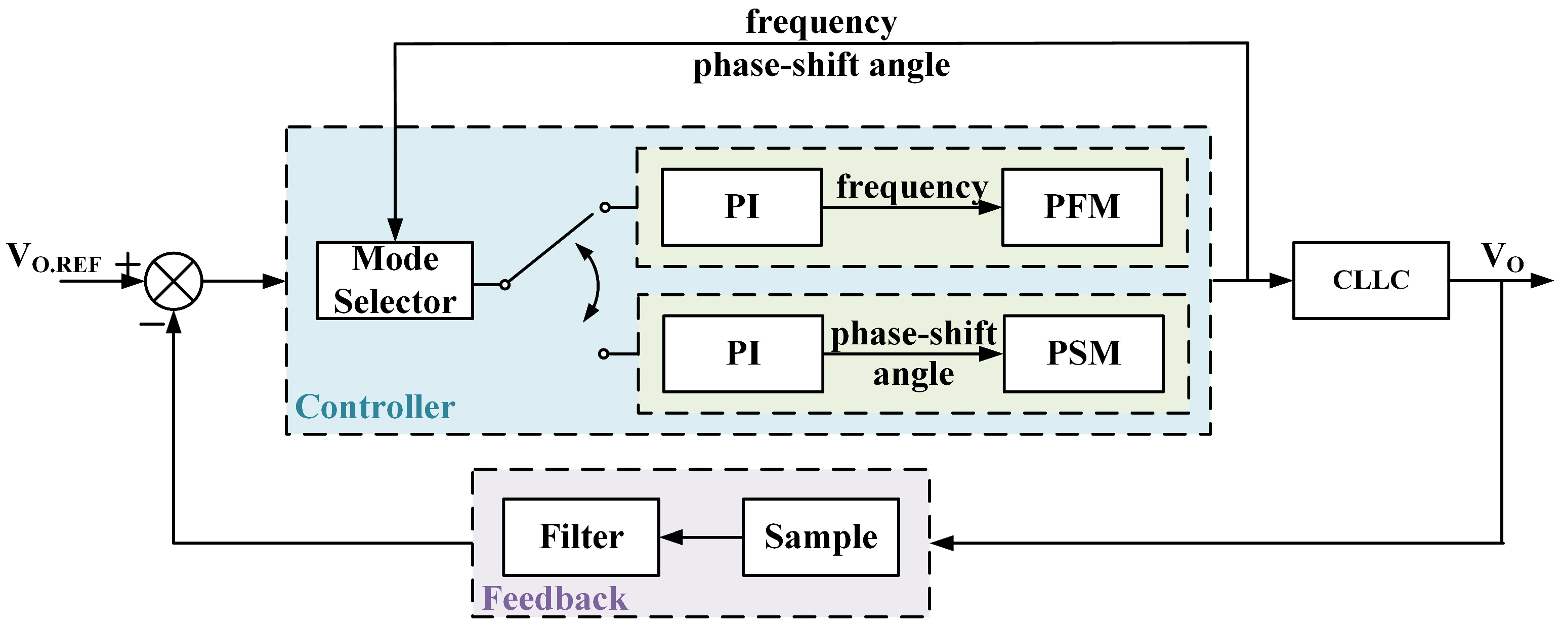
Figure 8 illustrates the elements of the hybrid modulation for CLLC resonant converters. The error, which is the difference between the user-set voltage reference and the feedback voltage, is input into the controller unit. Taking into account the current operating frequency and phase-shift angle, the controller unit selects the appropriate modulation technique to generate the driver signal, thereby achieving closed-loop control of the CLLC resonant converter. The blue section in
Figure 8 represents the basic structure of the controller unit, comprising the mode selector, the PFM modulator with its PI compensator, and the PSM modulator with its PI compensator. It is worth noting that the compensators are associated with the modulation methods individually, meaning that, when switching between modulation methods, the corresponding PI compensator will also switch accordingly. Based on the analysis of the gain and the design of loop stability compensation for CLLC resonant converters under PFM and PSM modulation mode in the previous section, the converter is capable of stable operation in a single modulation mode, which satisfies the output requirements of the converter in most scenarios.
However, when the converter operates at the highest switching frequency in PFM or the minimum phase-shift angle in PSM, tiny noise disturbances can trigger repetitive transitions between the two modulation modes, resulting in inevitable high-frequency oscillations in the output and consequently deteriorating the system’s dynamic response capability.
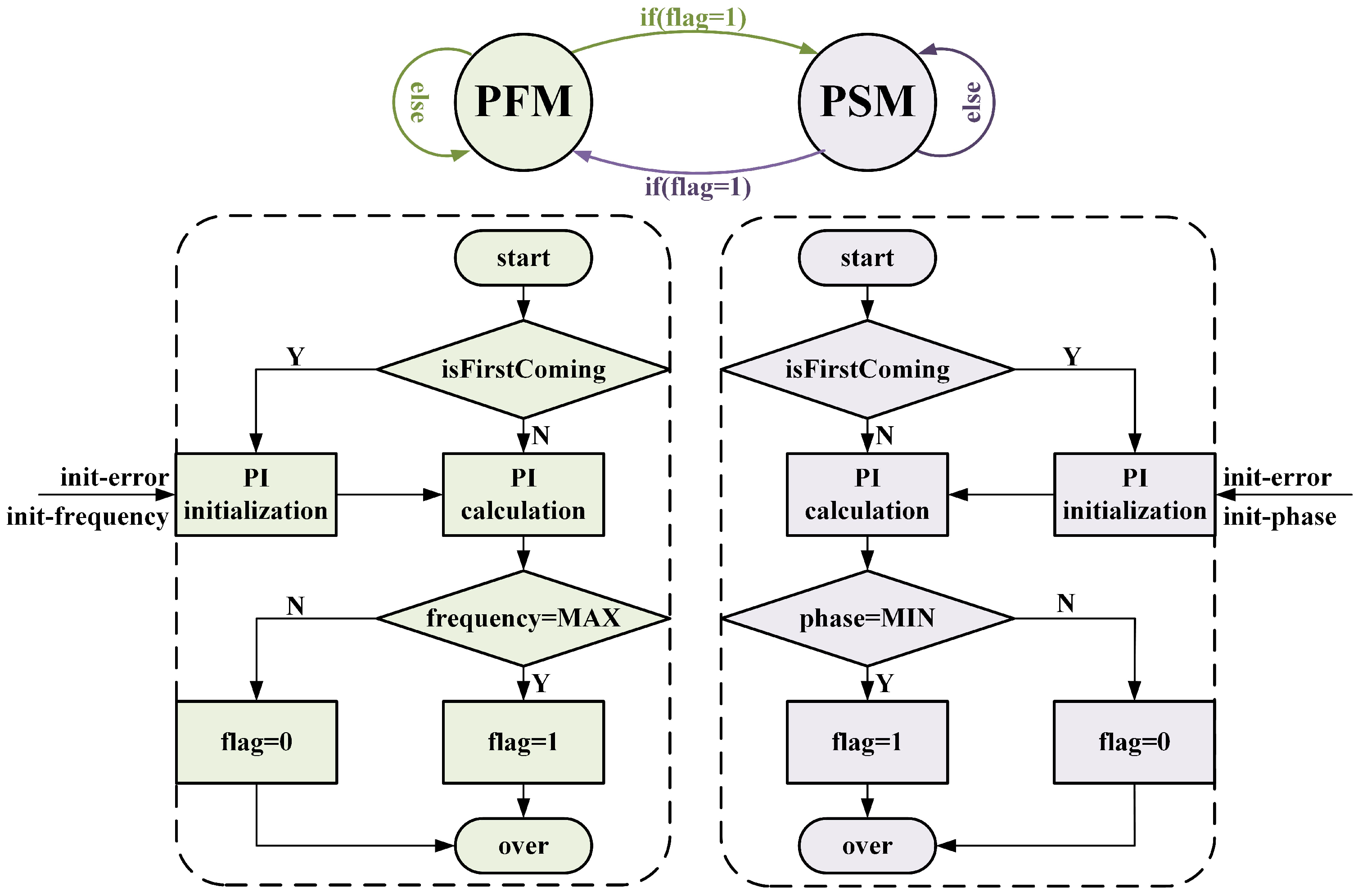
Figure 9 illustrates the detailed operational principle with hybrid modulation using the traditional mode selector method. After powering up the converter, the controller initially operates using the PFM modulation method. It first checks whether the initialization of the PI compensator is necessary. Once the initialization is completed or deemed unnecessary, the PI compensator calculates the switching frequency. When the calculated result matches the converter’s maximum operating frequency, the flag will be set to 1. Otherwise, it will remain as 0. The main state machine then evaluates the flag value to determine the modulation method for the next cycle. Specifically, if the flag is equal to 1, the converter can operate using the PSM method. Otherwise, it will continue using the current modulation method, namely PFM. Similarly, the transition from PSM modulation to PFM modulation is entirely symmetrical. Benefiting from the advantages of digital control techniques, the state machine can be executed periodically. In brief, there are two primary tasks when a new control instruction is incoming. During the control cycle, two primary tasks are executed step by step. Firstly, the PI compensator is activated to calculate the appropriate switching frequency or phase-shift angle based on the calculation results from the previous control cycle. Secondly, the corresponding modulation unit is activated to output a pulse that adjusts the operational state of the chopping unit. It is worth noting that the initial switching frequency and initial phase used for compensator parameter initialization remain unchanged due to the absence of necessary updates. However, the initial error is updated at the end of each control cycle, benefiting from the error analysis performed during the PI calculation process.
In summary, the traditional modulation mode selector method primarily relies on assessing the output frequency with PFM modulation and the output phase-shift angle with PSM modulation. It is worth noting that PI initialization executes only once during the controller’s startup, and the initialization parameters are not updated after this. This characteristic is also a contributing factor to the observed output voltage instability at critical states.
This approach is characterized by its simplicity, efficiency, and minimal computational overhead. However, when the converter operates in proximity to its critical state, the traditional modulation mode selector algorithm becomes vulnerable to noise interference, potentially leading to erroneous mode transitions. Additionally, due to the influence of the high-bandwidth PI compensator, these incorrect modulation mode switches can induce substantial output adjustments, resulting in avoidable voltage oscillations.
3. Proposed Dynamic Transition Algorithm
Based on the analysis above, to further enhance the performance of hybrid modulation, it is imperative to tackle the matter of compensator parameter updates, while simultaneously minimizing the influence of noise on mode switching.
This paper introduces an adaptive parameter updating method to mitigate the performance degradation resulting from improper parameter settings in the converter. Specifically, it compares the current modulation mode with the previous one to decide whether to update the compensator’s previous error and previous output. If the current modulation mode matches the previous one, parameter updates are skipped; otherwise, the latest error is employed to update the controller. Additionally, it incorporates an error analysis method and hysteresis comparison to prevent unnecessary mode changes at critical states. This method ensures that modulation mode transitions only occur when the judgment condition persists for several consecutive cycles. Compared to other improvement approaches in the field, this method offers greater flexibility in mode switching control due to its unique error analysis and hysteresis comparison. As a result, the potential risk of noise interference is further reduced.
Figure 10 illustrates the workflow of the proposed mode selector. As with the traditional mode selector method, after the converter starts up, the controller initially operates using the PFM modulation method. Firstly, the controller evaluates the need for initialization based on the last modulation mode. Once the initialization is either completed or considered unnecessary, the PI compensator calculates the switching frequency. If the calculated result matches the user-defined maximum frequency, and the error between the reference voltage and the output voltage exceeds the acceptable range, the counter is enabled. When the count value exceeds the hysteresis threshold, the modulation mode transitions to PSM in the next cycle. When the converter is currently operating using the PSM modulation method, its operation process is also similar to the former. Similarly, the first step is evaluating the need for initialization based on the last modulation mode. Once the initialization is either completed or considered unnecessary, the PI compensator calculates the phase-shift angle. If the calculated result matches the user-defined minimum phase-shift angle, and the error between the reference voltage and the output voltage exceeds the acceptable range, the counter is enabled. When the count value exceeds the hysteresis threshold, the modulation mode transitions to PFM in the next cycle.
In comparison to the traditional control methods, the proposed approach offers two key optimizations. Firstly, it supplements the conditions for the initialization of the PI compensator, automatically updating the initial error when the modulation modes differ between consecutive cycles, which reduces overshoot during the transient process of modulation mode switching. Secondly, it introduces hysteresis in the transition process, requiring the satisfaction of multiple consecutive conditions before allowing a modulation mode switch. For instance, the transition from PFM to PSM necessitates two specific conditions: firstly, the output modulation frequency must match the maximum modulation frequency; secondly, the output voltage should fall outside the precision error range defined by the user for a consecutive number of cycles. This significantly mitigates the issue of noise interference with the mode selector.
With these improvements, the converter is able to effectively utilize the capabilities of the PI compensator during the switch to a new modulation mode, resulting in a significant increase in the dynamic performance of the output.
4. Experimental Results and Discussion
To evaluate the robustness and feasibility of the proposed dynamic transition algorithm integrated with the hybrid modulation method, this section presents a 1 kW symmetric CLLC prototype with experimental results.
Due to manufacturing errors in the capacitors and inductors of the resonant tank, the operation performance of the CLLC resonant converter may differ from the theoretical analysis. To improve the accuracy, the resonant tank parameters are measured using the LCR meter after the prototype is assembled. All of the parameters of the prototype are shown in
Table 1. It is worth noting that the resonant capacitance is composed of a parallel combination of
nF film capacitors, rather than a single capacitor. The purpose of this approach is to flexibly adjust the capacitance parameters while ensuring maximum current and voltage tolerance to avoid damage to the resonant tank.
The test instruments and the symmetric CLLC prototype are depicted in
Figure 11, and they include a four-channel oscilloscope with a compatible Hall current probe and isolated voltage probe, a 750 V 5 kW DC power source, and a 5 kW DC load.
To facilitate the observation of experimental data, and are both saved. indicates the voltage between the midpoints of the two bridges in the chopping unit, which reflects the actual excitation signal of the resonant tank. The density of can also demonstrate the operating frequency of the converter. On the other hand, represents the output current of the converter.
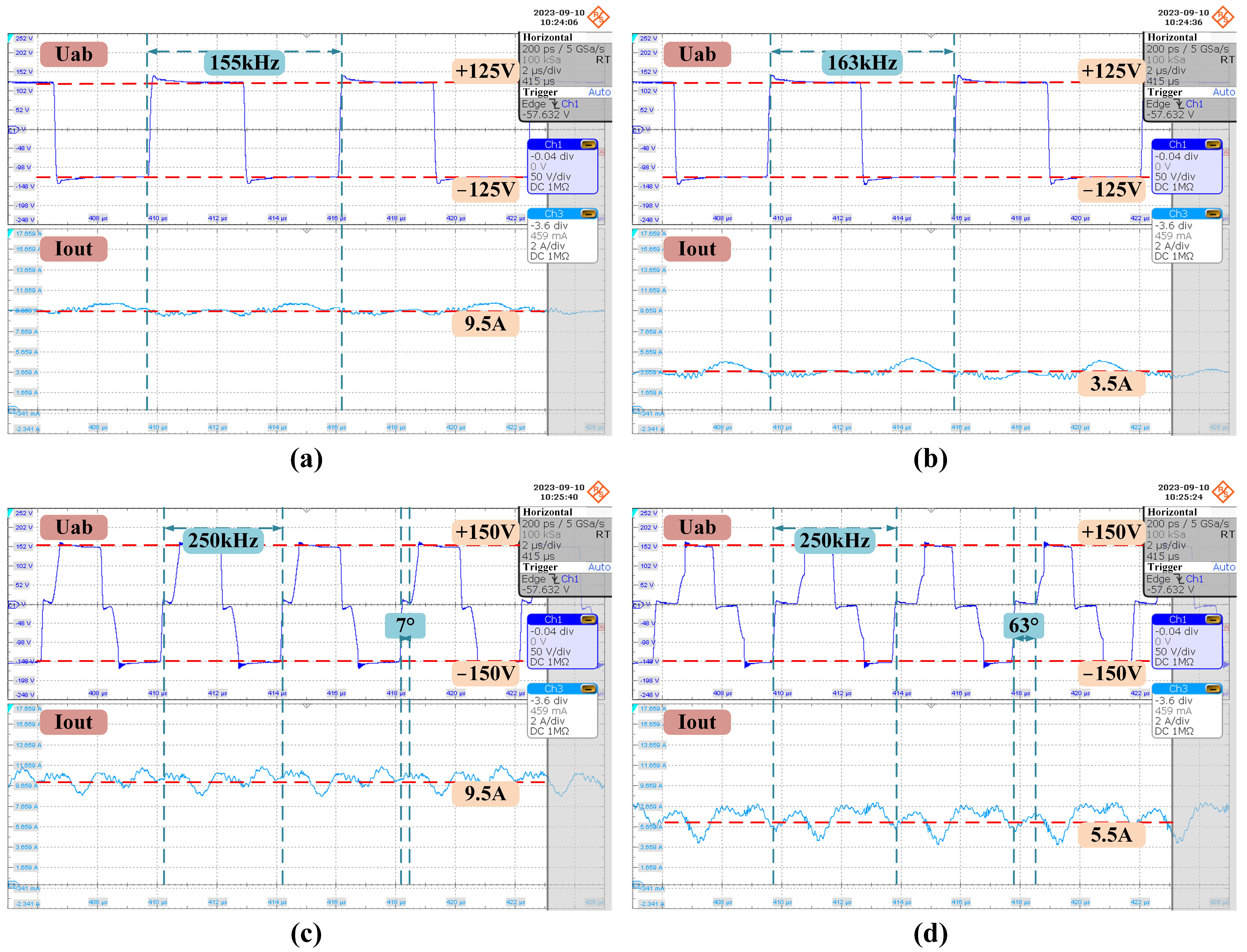
Figure 12 illustrates the typical operation waveforms with different loads captured by an oscilloscope. Under heavy load conditions, the resonant tank input waveform of the prototype using PFM, as shown in
Figure 12a, has a frequency of 155 kHz. Conversely, under light load conditions, the waveform of the prototype using PFM, as shown in
Figure 12b, operates at a frequency of 163 kHz. Similarly, under heavy load conditions, the resonant tank input waveform of the prototype using PSM, as depicted in
Figure 12c, exhibits a phase-shift angle of
, while, under light load conditions, the waveform of the prototype using PSM, as shown in
Figure 12d, features a phase-shift angle of
. It is worth noting the current ripple observed in
Figure 12, which represents common-mode noise caused by the switching of MOSFETs in the chopping unit. It is also worth noting that when the converter maintains a constant voltage output of 100 V, the current noise increases as the output power decreases.
Figure 13 demonstrates the closed-loop stability of the converter with a single modulation mode. When the converter’s output load steps up, the PFM compensator quickly responds to increase the output current, as shown in
Figure 13a. Conversely, when the converter’s output load steps down, the PFM compensator promptly decreases the output current to stabilize the voltage output, as illustrated in
Figure 13b. Similarly, when the converter operates in PSM mode, the compensator can quickly respond to adjust the output voltage, whether it is a step-up or step-down scenario, as depicted in
Figure 13c,d. The calculation results analyzed in the previous section for the PI compensator parameter settings corresponding to the PFM method and the PSM method can be directly applied. These parameters are set to ensure the stability of the converter while maximizing its theoretical dynamic response capability.
It is evident that when there is a load change, the converter with the appropriate and accurate parameter settings of the PI compensator can respond rapidly and adapt to a new steady state. This indicates that with a single modulation mode, the converter can achieve favorable dynamic and steady-state characteristics with the assistance of the corresponding compensator.
Based on trial-and-error, it is discovered that when the is equal to A, the converter operates in PSM mode with a relatively small phase-shift angle, and when the is equal to A, the converter operates in PFM mode with a relatively high switching frequency. These two load conditions not only ensure the stable operation of the converter in a single modulation mode before manually switching the load but also facilitate the observation of the converter’s response speed and adjustment capability. Based on the above analysis, the current probe of the oscilloscope is set to 2 A/div to display waveform details and the overall trend of changes while avoiding signal observation being affected by noise interference during the mode transition.
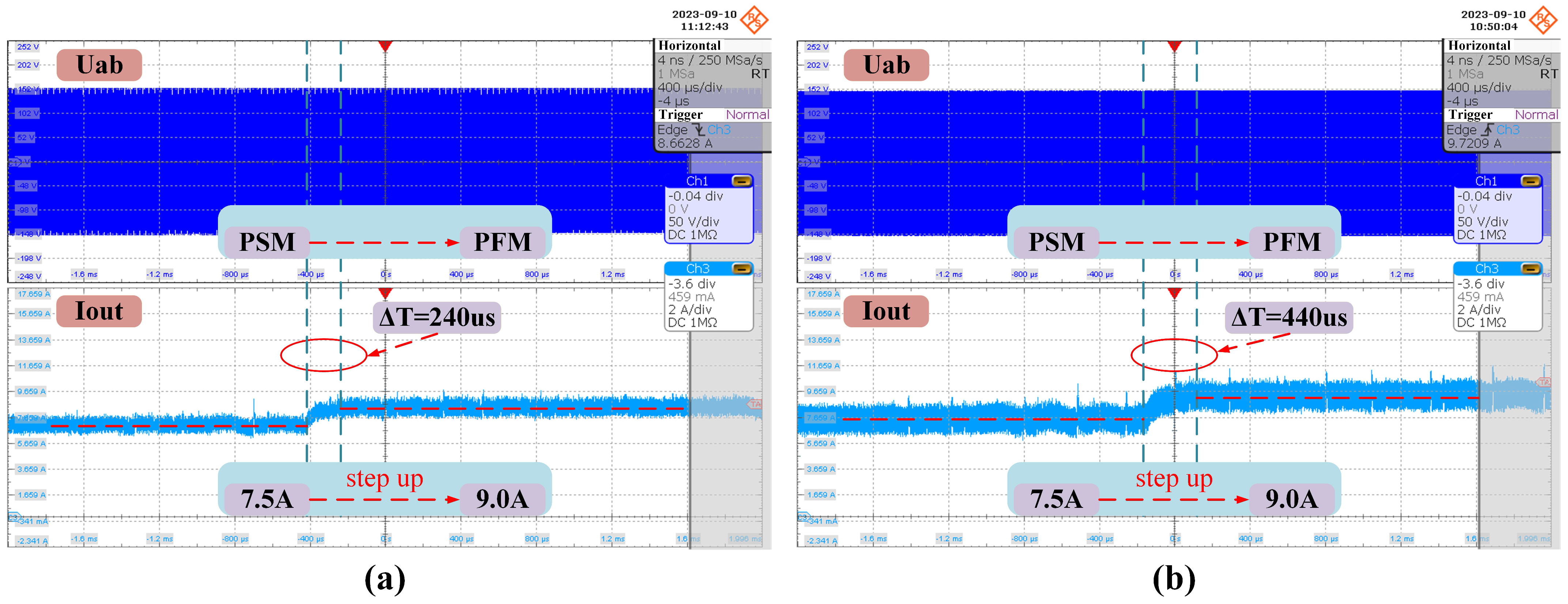
Figure 14 illustrates the dynamic response of the converter when the output load steps up from
A to
A under the same compensator settings. Among them, the implementation results of the converter with the proposed dynamic transition algorithm are shown in
Figure 14a, and it takes a total of 240
s to transition from the load change to entering the new steady state. However, under the same conditions, the converter using the traditional method takes 440
s, as shown in
Figure 14b. While both execution strategies can achieve the mode transition from PSM to PFM, the time consumed by the two methods differs by nearly a factor of two. This highlights that the proposed dynamic algorithm enhances the performance of hybrid modulation when the load increases.
Correspondingly,
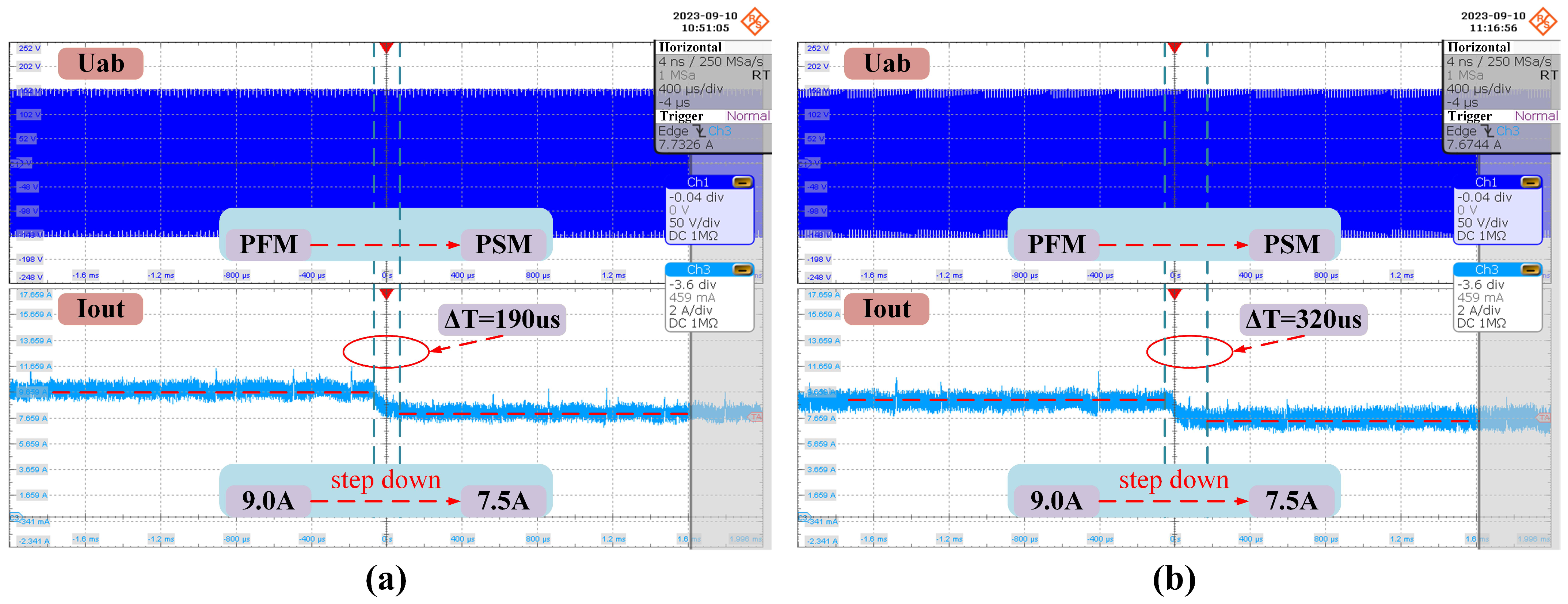
Figure 15 illustrates the dynamic response performance of the converter when the output load steps down from
A to
A using the same compensator settings. The output current of the prototype is presented in
Figure 15a, where it takes a total of 190
s to transition from PFM to PSM. In contrast, when the converter employs the traditional method, as shown in
Figure 15b, it takes a total of 320
s to switch from PFM mode to PSM mode. Consistent with the previous comparative results, the proposed algorithm is approximately twice as fast as the traditional method in this scenario.
Upon analyzing the experimental results stated above, it is found that the converter reaches a new steady state in only 240 s when the output current rapidly increases from A to A, which is a typical step-up testing scenario. This marks a 45% improvement in dynamic performance compared to traditional methods. Notably, in a single modulation mode, the compensator parameters for both methods are identical, indicating that error analysis and hysteresis comparison play a crucial role in the mode switching process. Moreover, under the test conditions where the output current rapidly decreases from A to A, which is a typical step-down testing scenario, the converter reaches a new steady state in only 190 s. This represents a 40% improvement in dynamic performance, demonstrating that the proposed method has a performance advantage under step-down conditions. Additionally, benefiting from the error analysis and the hysteresis comparison, the converter using the proposed method exhibits significantly reduced current ripple compared to the traditional method under the same conditions, which enhances its resistance to interference and increases the system’s robustness.
To summarize, the dynamic transition algorithm, with its excellent anti-interference ability, can help the converter to achieve a nearly 50% improvement in dynamic performance, whether in step-up or step-down conditions. This is critical for the efficient operation of the system. Based on this method, the performance of the hybrid modulation approach has been significantly enhanced, making it better suited for applications with a larger load regulation range.


