Abstract
This study aims to analyze the zero-voltage-switching (ZVS) region of a Triple-Active-Bridge (TAB) converter with five degrees of freedom. A TAB converter is an isolated converter derived from a dual-active-bridge (DAB) converter and composed of three full bridges (FBs) coupled to three winding transformers. To reduce the switching loss of the 12 active switches that compose 3 FBs, the ZVS operation is essential. However, owing to the numerous operation modes derived by five-phase shift ratios, ZVS analysis is complicated, particularly in the time domain. Therefore, this study presents the ZVS analysis model of the TAB converter based on the generalized harmonic approximation (GHA). Through the GHA of a TAB converter, the proposed model consists of unified formulas applicable to all operating ranges of the converter. Unified formulas consider all parameters, such as series inductance, port voltage, parasitic capacitance, transformer voltage, and turn ratio. In the proposed model, the ZVS area is confirmed using five-phase ratios with voltage modulation ratios as variables and verified using MATLAB and experiments.
1. Introduction
As a countermeasure to the greenhouse effect caused by fossil fuels, eco-friendly energy industries such as renewable energy sources, electric vehicles, ships, and direct-current (DC) grids are growing [1]. Energy storage systems (ESS) are essential in these renewable energy sources to compensate for intermittence and meet load demand [2,3]. The conventional solution for combining ESS with renewable energy is to use various converters independently. However, this approach increases the system volume and cost and reduces the life cycle of the ESS by generating circulating power between the converters. Moreover, limitations are observed in that an additional communication system is required to control the power transmission of each converter, making the entire system complex. To overcome these limitations, the demand for multiport converters (MPCs) has increased [4]. Compared to the approach using multiple two-port converters, MPCs exhibit a simple structure with fewer power switches and passive components, higher power density, and higher dynamics [5,6]. In addition, it can be applied to various sources, storage systems, and loads with various voltage and current ratings. Therefore, their applications are expanding from electric vehicles [7] and electric aircraft [8] to DC grids [9,10]. Because MPCs must support various voltage and current ratings for each port, galvanic isolation between different ports is required for safety [11]. Therefore, a multi-winding high-frequency transformer was used.
Among isolated MPCs, the triple-active-bridge (TAB) converter is a promising topology derived from a dual-active-bridge (DAB) converter. Three full bridges (FBs) are coupled through the three-winding transformer as shown in Figure 1 and unlike resonant-type converters, since additional passive elements are not required and power flow is formed through one transformer, power density can be increased compared to other MPCs [12,13,14]. Similar to a DAB converter, a TAB converter is operated through phase-shift modulation with five degrees of freedom consisting of two outer phases and three inner phases, which are the phase-shift ratios between the three FBs and between the legs of each FB.
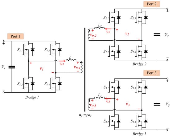
Figure 1.
Schematic of a TAB converter.
Similar to other FB converters, a TAB converter is composed of several power switches, and hard switching in the commutation process causes high losses. Therefore, soft switching is essential, particularly when the switching frequency increases. Zero-voltage switching (ZVS) is the most widely used soft-switching method in PSM operation converters. Satisfaction with the ZVS operation depends on the phase shift ratios, and the ZVS region of the DAB converter, which is a family with a TAB converter that operates through PSM with three degrees of freedom, has been analyzed. In [15,16], different dual phase-shift modulations are proposed, and triple phase-shift modulations are proposed in [17,18,19] to improve the operation efficiency of the DAB converter. Hence, using the time domain analysis, the DAB operation was separated into 12 operating modes in [20]. Furthermore, computationally intensive numerical approaches that incorporate the effects of parasitic capacitances were used to derive the ZVS region [21].
However, unlike a DAB converter, which has relatively few operating modes with three degrees of freedom, the five degrees of freedom of a TAB converter are derived from numerous operating conditions. Moreover, because the three FBs are coupled, equalizing the series inductance by substituting one side is impossible. Therefore, port-voltage superposition in the three-winding transformer must be considered. Because of these issues, the ZVS analysis of the TAB converter is more complicated than that of the DAB converter.
A ZVS analysis of a TAB converter was attempted in [22]; however, it considered only an outer phase shift and did not consider an inner phase shift. In addition, the voltage superposition in the transformer and the effect of parasitic capacitance were neglected. To analyze the ZVS accurately, owing to the amount of charge in the parasitic capacitance of the metal-oxide-semiconductor-field-effect-transistor (MOSFET), not only the direction of the inductor current but also the minimum magnitude must be considered when discharging the capacitor [23,24]. In [25], an approach for analyzing the ZVS region of a TAB converter using a Thevenin-equivalent circuit was proposed. The series inductances of the three FBs were substituted through a Thevenin equivalent circuit, and the voltage superposition of the transformer was analyzed according to the switching state of the switches. In addition, the parasitic capacitor of the MOSFET was considered, and the amount of current required to establish ZVS was derived. However, because the TAB converter was analyzed in the discontinuous time domain, numerous conditions were derived based on the switching states of 12 switches. Therefore, various formulas were required for application in numerous cases; consequently, ZVS could not be analyzed using a unified formula. For example, to establish whether ZVS operates, the inductor current has to be derived. The slope of the inductor current is determined by the potential difference between the switching pole voltage and the transformer voltage. Therefore, in time domain analysis, numerous inductor current slopes must be derived according to the numerous operating regions of the TAB converter. Moreover, in the case of a multi-active bridge converter with a structure in which more FBs were added, the limitation of the time-domain analysis was even more pronounced. In addition, additional conversions of the Thevenin equivalent circuit were required. Consequently, the application of different equivalent circuits according to the viewpoint of each FB is required, resulting in difficulties in intuitive interpretation.
To address the limitations of time-domain analysis, this study presents a TAB converter ZVS region analysis model based on the generalization-harmonic approximation (GHA). The switching-pole voltage of a TAB converter is a periodic function of a square or quasi-square wave. Therefore, it can be expressed as a unified formula using the cumulative sum of harmonics through a Fourier series. This approach can directly derive the inductor current and voltage of a three-winding transformer and the switching pole voltage. Therefore, regardless of the conditions, a unified formula can be derived for the entire switching operation area. The effect of the parasitic capacitor was also considered, and the magnitude of the minimum inductor current for discharging was derived using the energy balance equation concept applied in the ZVS analysis of the DAB converter [26]. The proposed approach and model are simple to extend and apply, even to a multi-active-bridge converter that adds FBs and can be easily calculated through MATLAB. The remainder of this paper is organized as follows: a description of the TAB converter and derivation of the harmonic form; analysis of commutation processes in the FB; derivation of conditions to achieve ZVS considering parasitic capacitors; and derivation of the ZVS analysis model. The proposal is verified using MATLAB simulations and experiments.
2. Operation and the GHA Modeling of the TAB Converter
2.1. Operating Principles
The equivalent circuit model of a TAB converter is shown in Figure 2. Considering the turn ratio of the transformer, the components of the circuit are replaced as follows:
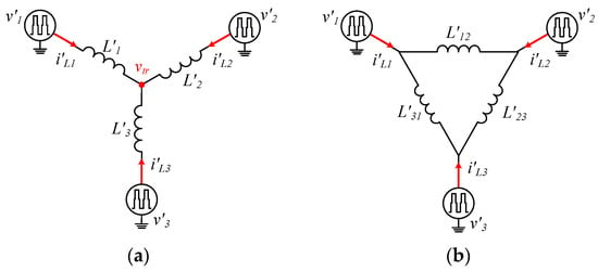
Figure 2.
Equivalent circuit model of a TAB converter: (a) Y-connected model; (b) Δ-connected model.
In (1), the x means unspecific FB. For the unified formulas, the post equations were derived using x, y, and z. The actual TAB converter is in the form of the Y-connected structure, as shown in Figure 2a, but the Δ-connected model shown in Figure 2b is also used in circuit analysis. Through the Y-Δ conversion, the equivalent inductance L′xy between unspecific two FBs x and y in the Δ-connected model is derived as follows:
Figure 3 shows the operating waveform of the TAB converter. In the waveforms, αx is the inner phase shift ratio between the leading leg (Sx.1, Sx.2) and lagging leg (Sx.3, Sx.4), and ϕxy is the outer phase shift ratio between FB x and y (ϕxy = ϕx − ϕy). The inner phase shift as α results in an equal switching state formed in the leading and lagging legs, and the voltage of the switching pole becomes a quasi-square wave. The voltages of each switching pole are out of phase as ϕ, and all voltages are superposed to the transformer and form the vtr. Consequently, the inductor current i′Lx and delivered power of each FB are determined by the potential difference between the switching pole and transformer.
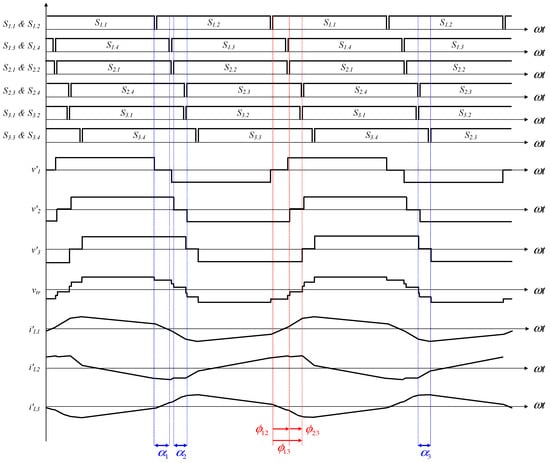
Figure 3.
Operating waveforms of a TAB converter.
2.2. GHA Modeling
In the mathematical modeling of the TAB converter, the conventional method of deriving the state equation according to the on-off state of the power switch is too complex to derive the formula because of the 12 power switches with five degrees of freedom. As an alternative to settling this problem, GHA modeling was used. As the switching of the FB is periodic, a Fourier series can be used. Therefore, the switching pole voltage v′x can be expressed as the cumulative sum of the odd harmonics, as follows:
The transformer neutral-point voltage vtr is determined using three voltage sources and three series of inductances, as shown in Figure 2a. Through the principle of superposition between multiple sources, vtr can be expressed as
By ignoring the voltage sources of FB y and z as short circuits, the function F{v′x(t)} for v′x of vtr is as follows:
Therefore, vtr can be derived using (4) and (5), and the vtr.x the transformer voltage viewed from FB x can be expressed as:
The inductor current i′Lx can be directly calculated through the voltage sources on the switching pole and transformer side derived in (3) and (5). However, it is very complicated to derive owing to the variables (ϕx, ϕy, ϕz, αx, αy, αz) of voltage sources. Alternatively, it can be derived indirectly through the Δ-connected model shown in Figure 2b. (2) and (3), the inductor current i′Lxy between FB x and y is derived as follows:
The Axy and the Bxy are:
By applying the process of (7) to (9) between the FB x and z, i′Lx can be finally derived as:
3. Zero Voltage Switching
An ideal MOSFET consists of only a channel and body diode, and in this case, only the inductor current direction in the commutation process is used to confirm the ZVS operation. However, capacitance exists in an actual MOSFET, and this parasitic capacitor stores charge during the turn-off period of the switch. Therefore, in the commutation process, before the switch turns on, the energy of the parasitic capacitor must be completely discharged to achieve zero voltage in the switch. Hence, the direction and magnitude of the inductor current should be considered to confirm ZVS operation.
Figure 4 shows the commutation process in dead time before the switch is turned on. Because the commutation process is instantaneous, the voltages on the switching pole and transformer do not change, and the voltage at the transformer port is expressed as the initial magnitude of the process as Vtr.x the DC value. Figure 4a,b show the switching cases without inner phase shift (αx = 0), and the leading and lagging legs operate simultaneously. Further, Figure 4c–f shows the switching cases with an inner phase shift (αx ≠ 0), and the leading and lagging legs operate differently. Before each switch is turned on, the current flows in the direction of discharging the parasitic capacitor Coss.x, as indicated by the orange line, and the reference direction of each current is indicated by a red arrow. The upper and lower switches of one leg operate complementarily; therefore, if one switch of the leg satisfies the condition for the ZVS operation, the other switch can also perform the ZVS operation. Because of the nonlinear capacitance characteristics of MOSFETs, direct calculation of the energy stored in a parasitic capacitor is difficult. Therefore, the energy to be discharged during the commutation process and the magnitudes of the minimum inductor energy and current are derived by applying the energy-balance equation. During FB operation, two parasitic capacitors in one switching leg exchange energy with each other and do not transfer to the other components. Consequently, the energies of the two capacitors on one leg can be ignored, and the energy balance equation for the commutation process is as follows:
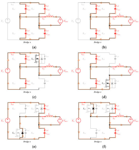
Figure 4.
Commutation process. (a) Case A: before Sx.1 and Sx.4 turn on. (b) Case A′: before Sx.2 and Sx.3 turn on. (c) Case B: before Sx.1 turns on. (d) Case B′: before Sx.2 turns on. (e) Case C: before Sx.3 turns on. (f) Case C′: before Sx.4 turns on.
Es, EL, and Etr.x represent the source, inductor, and transformer-side energies, respectively, during commutation.
Integration sections t0–td are the commutation process sections before the subject switches on. Meanwhile, the minimum magnitude condition of the inductor current and energy for ZVS operation occurs when the current and energy become zero at the end of the commutation process, as shown in (13). Applying (12) to (11), we obtain the following inequality:
Ediff is the energy difference between the source and transformer sides. Because the energy flow changes depending on the direction of the inductor current, the sign follows that of the inductor current. As shown in (15), when EL (t0) is higher than Ediff, the parasitic capacitor can be discharged entirely through inductive energy, and ZVS operation is established. If Ediff has a negative value, the energy supply is higher than the energy consumption between the two voltage sources. Therefore, unlike the minimum inductor current and energy conditions for ZVS in (13), the surplus energy is stored in the inductor, the parasitic capacitor can be sufficiently discharged regardless of the magnitude of the initial inductive energy, and ZVS operation is obtained.
3.1. Without Inner Phase Shift (αx = 0)
In Case A in Figure 4a, a closed circuit is formed without an input voltage source, and the direction of the inductor current is negative. The circulating energy during the commutation process is supplied from the voltage source on the transformer side, and the input and inductor currents are derived using the node equation as follows:
Applying (16) and (17) to (12) and (14), Ediff can be expressed as
Conversely, in case A′ in Figure 4b, where the inductor current is in the positive direction, Ediff is obtained as
If Ediff derived from (18) and (19), satisfies the energy inequality in (15), then the ZVS operation is established for cases A and A′.
3.2. With Inner Phase Shift (αx ≠ 0)
In Case B in Figure 4c, the inductor current is negative, the leading and lagging legs do not operate simultaneously because of the inner phase shift, and a closed circuit is formed with the input voltage source. The input and inductor currents derived from the node equation are:
Conversely, in case B′ in Figure 4d, where the inductor current is in the positive direction, Ediff is:
Similarly, if Ediff derived from (22) and (23) satisfies the energy inequality in (15), a ZVS operation is established. Cases B′ and C, which have an inner phase shift and the same inductor current direction for the discharge parasitic capacitor, have the same Ediff formula, and cases B and C′ also have the same. Therefore, Ediff can be defined as
As in (14), the sign of Ediff in (24) and (25) follows that of the inductor current, as shown in Figure 4. Finally, the minimum magnitude of the inductor current required to satisfy the ZVS operation in each case is listed in Table 1. Applying Vtr.x, Vx, and iL.x derived in Section 2.2 to the equations in Table 1, the ZVS operation can be confirmed. For example, when the turn-on point of the switch in full bridge x is t0, the transformer side voltage and inductor current, which are variables to confirm whether ZVS is established, are as follows:

Table 1.
ZVS operating conditions for each switching case.
4. Simulation and Experimental Results
The operation of the TAB converter involves seven variables: five phase-shift ratios and two voltage-modulation ratios.
However, simulations can only have two variables because they use one dimension as the output in three dimensions. Therefore, the ZVS analysis model was simulated in two parts using MATLAB, as listed in Table 1. A case in which use the outer phase shift ratio ϕ as variables; a case in which use voltage modulation ratio m as variables.
4.1. Case A (Variable: ϕ)
Based on the proposed ZVS analysis model in Table 1, the MATLAB simulation results of the ZVS operation region of the TAB converter using ϕ as a variable are shown in Figure 5. The red area is the region where ZVS is performed in the leading leg, the blue area is the lagging leg, and the purple area is the region where ZVS is performed on all legs. The empty area represents the hard-switching region.
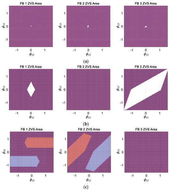
Figure 5.
ZVS operation region according to outer phase shift ratio ϕ variation. (a) m12 = m13 = 1 and α1 = α2 = α3 = 0. (b) m12 = 1.5, m13 = 0.75 and α1 = α2 = α3 = 0. (c) m12 = 1.5, m13 = 0.75 and α1 = 0.46π, α2 = 0.67π, α3 = 0.
Figure 5a shows the ZVS region when the voltage modulation ratio of the three FBs is 1:1:1, and the ZVS operation is assured in all FBs except under extremely light-load conditions. Figure 5b shows the ZVS region under the condition that the voltage modulation ratios of FB 2 and FB 3 are 1.5 and 0.75 based on FB 1. In FB 2, which has a higher equivalent voltage than the other two FBs, ZVS is ensured regardless of the phase shift ratios, but in FB 1 and FB 3, hard switching occurs depending on the phase conditions. In particular, FB 3, which had the lowest voltage, caused hard switching over a wide region. A comparison of Figure 5a,b confirms that soft and hard switching are critically determined by the voltage modulation ratio.
Meanwhile, the effective value of the switching pole voltage can be adjusted through the inner phase shift ratio α as (3). The fundamental value of each FB switching pole voltage can be matched through a simple calculation using arccosine. However, because only the fundamental wave components matched, the actual effective voltage could be reduced. Figure 5c shows the ZVS region when the magnitude of the fundamental value of all FB’s switching pole voltages is matched by applying an inner phase shift ratio of 0.46π and 0.67π to FB 1 and FB 2, respectively. By matching the magnitudes of the switching pole voltages, ZVS operation under light-load conditions was ensured in all FBs. However, the ZVS regions between the leading and lagging legs differ because of unstimulated switching. This results from the phase of the inductor current: the leading leg facilitates the ZVS operation when transmitting power, and the lagging leg facilitates the ZVS operation when receiving power.
Figure 6 shows the simulation results of the operation waveform using MATLAB to verify the proposed GHA-based ZVS analysis model shown in Figure 5. In a switching leg, indicating the upper switch turn-on as ‘1’ and the lower switch turn-on as ‘−1’, the corresponding switching pole voltage is listed in Table 2. In Figure 6a–c, ϕ12 and ϕ13 are set as −0.05π and 0.05π, respectively, to confirm the operation waveform in the light load area where ZVS operation is difficult.
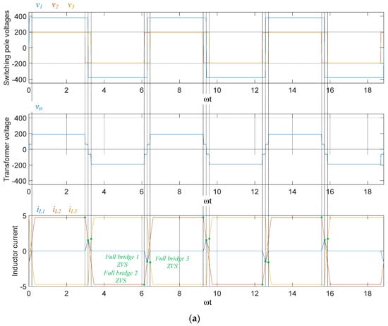
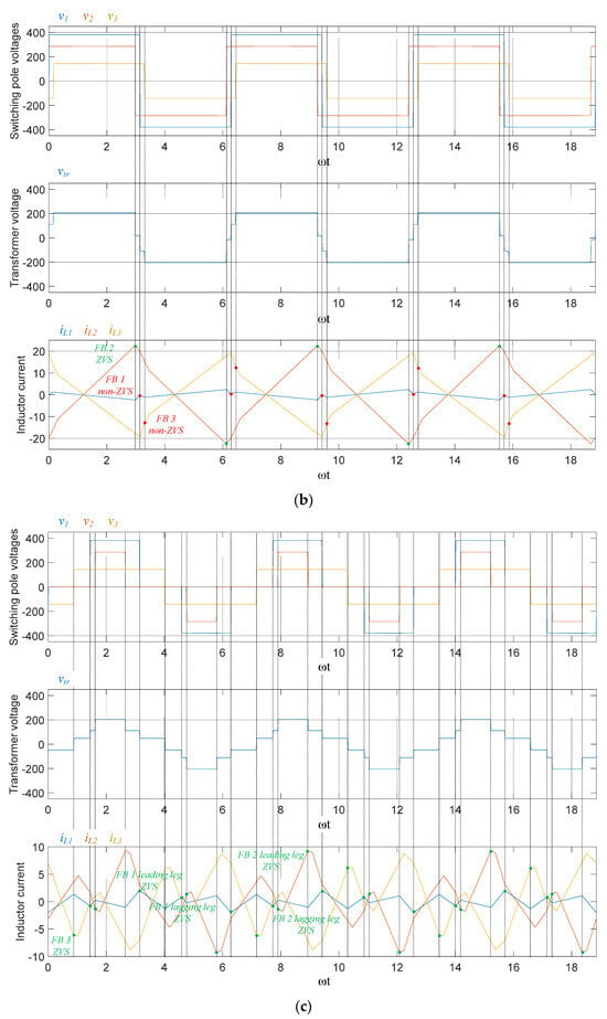
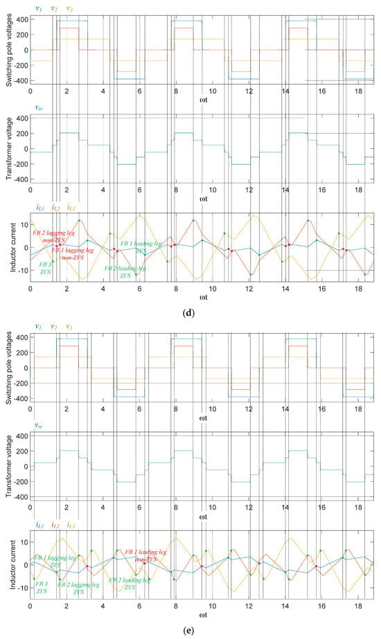
Figure 6.
TAB converter operation waveform. (a) α1 = α2 = α3 = 0, m12 = m13 = 1, ϕ12 = −0.05π, ϕ13 = 0.05π. (b) α1 = α2 = α3 = 0, m12 = 1.5, m13 = 0.75, ϕ12 = −0.05π, ϕ13 = 0.05π. (c) α1 = 0.46π, α2 = 0.67π, α3 = 0, m12 = 1.5, m13 = 0.75, ϕ12 = −0.05π, ϕ13 = 0.05π. (d) α1 = 0.46π, α2 = 0.67π, α3 = 0, m12 = 1.5, m13 = 0.75, ϕ12 = −0.05π, ϕ13 = 0.16π. (e) α1 = 0.46π, α2 = 0.67π, α3 = 0, m12 = 1.5, m13 = 0.75, ϕ12 = −0.05π, ϕ13 = −0.16π.

Table 2.
Switching pole voltage according to the switching state.
Figure 6a shows the operating waveform under the conditions shown in Figure 5a; owing to the voltage ratio of 1:1:1, all FBs perform ZVS operation without an inner phase shift. Figure 6b shows the operation waveform under the condition of Figure 5b; except for FB 2, the remaining FBs cannot perform the ZVS operation. In particular, in the case of FB 3, which has the lowest voltage ratio, the inductor current deviates significantly from the condition for performing ZVS. Figure 6c shows the operating waveform when the effective voltage of the switching pole was adjusted by applying an internal phase shift to the FB, as shown in Figure 5c. Because of the asynchronous operation of the leading and lagging legs, the switching-pole voltage became a quasi-square wave. Therefore, the effective values of the voltage are matched, and ZVS operation is ensured for all FBs in the light-load area. In addition, Figure 6d,e show the operation waveforms at the points in Figure 5c, where the ZVS is operated on only one leg of the FB.
4.2. Case B (Variable: m)
The simulation results for Case B, which used m as a variable, are shown in Figure 7. Figure 7a shows the ZVS region under the rated load conditions. All FBs ensured ZVS operations. However, in Figure 7b, which shows the light load conditions, it can be confirmed that the ZVS operation is not achieved according to the voltage modulation ratio. In particular, these results are noticeable for FB with relatively low voltage ratios. Figure 7c shows the ZVS region when an inner phase shift is applied to the FB with a higher voltage ratio. Compared to FB 1, when the voltage modulation ratios of FB 2 and FB 3 are higher than 1, the inner phase shift is applied and varied in proportion to the voltage modulation ratio. In FB 1, ZVS is ensured in the entire area, and in FB 2 and FB 3, ZVS operations are improved in parts where m12 and m13 are greater than 1.
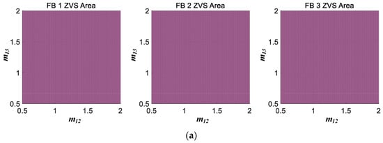
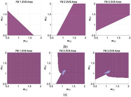
Figure 7.
ZVS region according to voltage modulation ratio m variation. (a) ϕ12 = ϕ13 = 0.5π and α1 = α2 = α3 = 0. (b) ϕ12 = ϕ13 = 0.05π and α1 = α2 = α3 = 0. (c) ϕ12 = ϕ13 = 0.05π and α1 = 0, α2 = 2cos(1/m12), α3 = 2cos(1/m13).
Figure 8 shows the operating waveform of the TAB converter used to verify the ZVS analysis model shown in Figure 7. The voltage modulation ratios m12 and m13 are 0.85 and 2, respectively. The simulation results show the operation waveforms under rated load, light load, and variable inner phase-shift conditions.
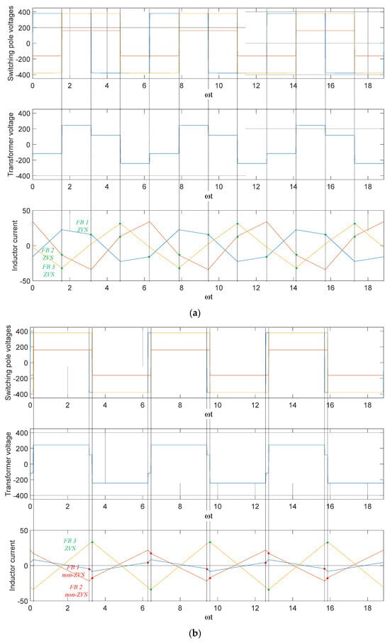
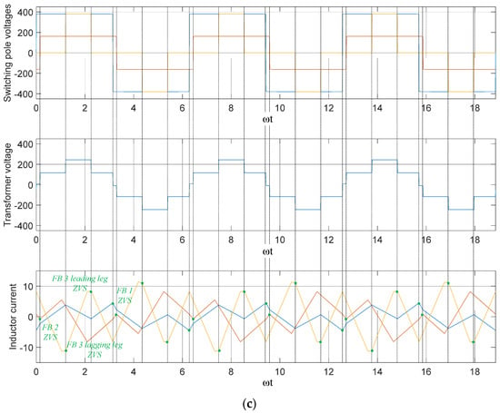
Figure 8.
TAB converter operation waveform. (a) α1 = α2 = α3 = 0, m12 = 0.85, m13 = 2, ϕ12 = 0.5π, ϕ13 = 0.5π. (b) α1 = α2 = α3 = 0, m12 = 0.85, m13 = 2, ϕ12 = 0.05π, ϕ13 = 0.05π. (c) α1 = α2 = 0, α3 = 0.66π, m12 = 0.85, m13 = 2, ϕ12 = 0.05π, ϕ13 = 0.05π.
Figure 8a shows the simulation results under the rated load conditions, as shown in Figure 7a; all FBs perform the ZVS operation. Figure 8b shows the TAB converter operation waveform under the light-load condition, as shown in Figure 7b. Except for FB 3, which has the highest voltage level, the remaining FBs do not achieve ZVS operation. Figure 8c shows that the operation waveform under the inner phase-shift ratio varies according to the voltage modulation ratio to match the effective voltages of the switching poles, as shown in Figure 7c. An inner phase shift of 0.66π is applied only to FB 3 and owing to the asynchronous operation of the leading and lagging legs, the switching pole voltage becomes a quasi-square wave. Therefore, the effective values of the switching pole voltage are matched in FB 1 and FB 3, and the effective voltage ratios of FB 2 with the other FB are also close to 1, ensuring ZVS operation in all FBs.
4.3. Prototype Experiment Results
An experiment was conducted using a prototype TAB converter to validate the proposed GHA-based ZVS analysis model. The prototype experiment was a 1/10 scale of the simulation, as shown in Figure 6. The switching-pole voltage and inductor current were measured at the operating points of the TAB converter. Moreover, Vds and Vgs were measured to observe the ZVS operation. The parameters of the prototype TAB converter used in this study are provided in Table 3.

Table 3.
Prototype TAB converter parameters.
Figure 9 shows the prototype TAB converter and Figure 10, Figure 11, Figure 12, Figure 13 and Figure 14 show the experimental results for the TAB converter at each operating point in Figure 6. The experimental results were separated according to FB. Under the condition of no inner phase shift, if the ZVS of only one switching leg is assured, the ZVS operation is assured in all MOSFETs; therefore, Vgs and Vds were measured only in the leading leg in Figure 10 and Figure 11. Under the condition of an inner phase shift, Vgs and Vds were measured for both the leading and lagging legs, as shown in Figure 12, Figure 13 and Figure 14. Vds is the voltage across the MOSFET and can be used to confirm whether the parasitic capacitor is discharged. Therefore, when the ZVS operation is performed, Vgs for the switch turn-on becomes positive after Vds becomes zero. However, if the ZVS operation is not performed, Vgs becomes positive before Vds becomes zero.
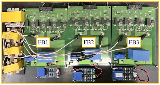
Figure 9.
Prototype TAB converter.
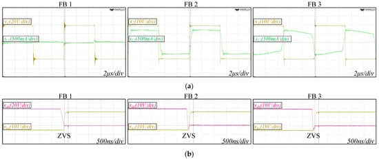
Figure 10.
Prototype experiment results of the TAB converter operating point in Figure 6a (α1 = α2 = α3 = 0, m12 = m13 = 1, ϕ12 = −0.05π, ϕ13 = 0.05π). (a) Switching pole voltage and inductor current. (b) Gate-source and drain-source voltages of MOSFET.
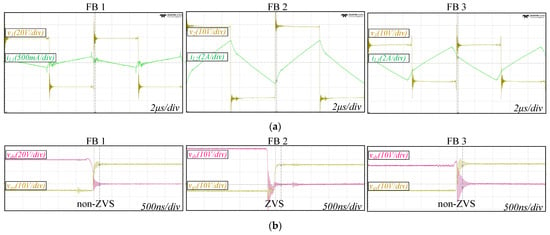
Figure 11.
Prototype experiment results of the TAB converter operating point in Figure 6b (α1 = α2 = α3 = 0, m12 = 1.5, m13 = 0.75, ϕ12 = −0.05π, ϕ13 = 0.05π). (a) Switching pole voltage and inductor current. (b) Gate-source and drain-source voltages of MOSFET.
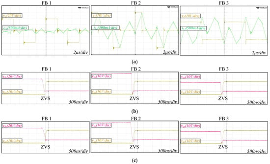
Figure 12.
Prototype experiment results of the TAB converter operating point in Figure 6c (α1 = 0.46π, α2 = 0.67π, α3 = 0, m12 = 1.5, m13 = 0.75, ϕ12 = −0.05π, ϕ13 = 0.05π). (a) Switching pole voltage and inductor current. (b) Gate-source and drain-source voltages of the leading leg MOSFET. (c) Gate-source and drain-source voltages of the lagging leg MOSFET.
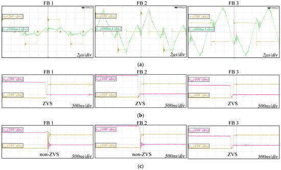
Figure 13.
Prototype experiment results of the TAB converter operating point in Figure 6d (α1 = 0.46π, α2 = 0.67π, α3 = 0, m12 = 1.5, m13 = 0.75, ϕ12 = −0.05π, ϕ13 = 0.16π). (a) Switching pole voltage and inductor current. (b) Gate-source and drain-source voltages of the leading leg MOSFET. (c) Gate-source and drain-source voltages of the lagging leg MOSFET.
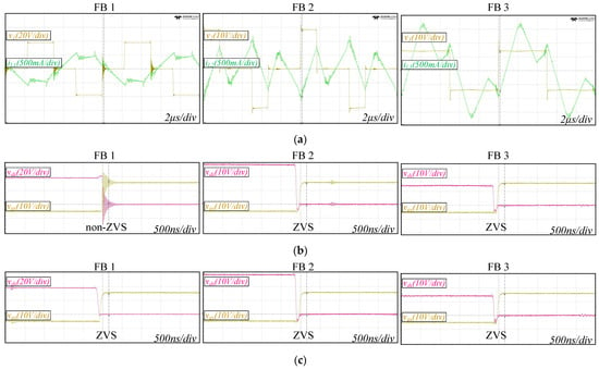
Figure 14.
Prototype experiment results of the TAB converter operating point in Figure 6e (α1 = 0.46π, α2 = 0.67π, α3 = 0, m12 = 1.5, m13 = 0.75, ϕ12 = −0.05π, ϕ13 = −0.16π). (a) Switching pole voltage and inductor current. (b) Gate-source and drain-source voltages of the leading leg MOSFET. (c) Gate-source and drain-source voltages of the lagging leg MOSFET.
A slight difference was observed in the experimental results owing to the parasitic resistance of the series inductor and resonance caused by the parasitic inductance and capacitance inside the SiC MOSFET. Overall, the inductor current and switching voltage waveforms are consistent with the GHA modeling-based simulation results shown in Figure 6. It can be seen in Figure 11 and Figure 12 that the voltage modulation ratio between the FBs affects the ZVS operation, and the effective value of the switching pole voltage matching through an internal phase shift can improve the ZVS operation performance. Contrary to the conventional concept that ZVS is assured only when the direction of the inductor current is appropriate during switching, when the inductor current of FB 2 has a negative value during lagging leg switching, the FB 2 lagging leg does not perform ZVS, as shown in Figure 13. This implies that the parasitic capacitor of the MOSFET is not sufficiently discharged. These results are consistent with those of the proposed ZVS analytical model and the simulations shown in Figure 5 and Figure 6, respectively.
5. Conclusions
This study provides a GHA-based ZVS analysis model of a TAB converter. The TAB converter has difficulty modeling and analyzing the ZVS operation in the time domain owing to numerous operation modes using five phase variables. Therefore, in this study, a TAB converter was modeled using a GHA based on the periodicity of the FB switching pole. In addition, a ZVS analysis of the FB was performed using the energy balance equation, and the minimum inductor energy and current conditions were derived. By applying the GHA model to the energy and current conditions for ZVS operation, a ZVS analysis model of the TAB converter was proposed that can be universally applied in all operating modes of the TAB converter. The ZVS operating range was derived using a ZVS analysis model simulation, and the effects of the outer phase shift ratio, inner phase shift ratio, and voltage modulation ratio on the ZVS operation were analyzed. Experiments were performed using a 1/10 scale prototype TAB converter, and the validity of the GHA and ZVS analysis models was verified by matching them with simulation results. As a result of the simulation and 1/10 scale experiment, it can be seen that the lighter the load condition and the lower the effective switching pole voltage ratio, the more difficult it is to perform ZVS operation, and hard switching occurs. The inner phase shift is a method of matching the effective switching pole voltage ratio, lowering the effective voltage size of the FB switching pole with a high voltage ratio, and making it possible to achieve the ZVS of all FBs. Considering that the Y-delta conversion in the TAB converter is a conversion method derived by the superposition of circuits, the DAB converter equivalent circuit can be derived in the multi-active-bridge converter through the principle of superposition. Therefore, the proposed GHA-based ZVS analysis model can be extended and applied to multi-active bridges, such as quadruple-active or penta-active bridges.
Author Contributions
Conceptualization, H.-J.B.; methodology, H.-J.B.; software, H.-J.B., and J.-M.P.; validation, H.-J.B., and J.-M.P.; formal analysis, H.-J.B.; investigation, H.-J.B.; resources, H.-J.B., and J.-M.P.; data curation, H.-J.B., and J.-M.P.; writing—original draft preparation, H.-J.B.; writing—review and editing, H.-J.B., and J.-M.P.; visualization, H.-J.B.; supervision, J.Y., and C.-Y.W.; project administration, J.Y., and C.-Y.W.; funding acquisition, J.-M.P. All authors have read and agreed to the published version of the manuscript.
Funding
This research was supported by grants from the International Energy Joint R&D Program of the Korea Institute of Energy Technology Evaluation and Planning (KETEP), granted financial resources from the Ministry of Trade, Industry, and Energy, Republic of Korea (20208510070060).
Data Availability Statement
Data are contained within the article.
Conflicts of Interest
The authors declare no conflict of interest.
References
- Dincer, I. Renewable energy and sustainable development: A crucial review. Renew. Sustain. Energy Rev. 2000, 4, 157–175. [Google Scholar] [CrossRef]
- Fuente, D.V.; Rodríguez, C.L.T.; Garcerá, G.; Figueres, E.; Gonzalez, R.O. Photovoltaic Power System with Battery Backup with Grid-Connection and Islanded Operation Capabilities. IEEE Trans. Ind. Electron. 2013, 60, 1571–1581. [Google Scholar] [CrossRef]
- Hadjipaschalis, I.; Poullikkas, A.; Efthimiou, V. Overview of current and future energy storage technologies for electric power applications. Renew. Sustain. Energy Rev. 2009, 13, 1513–1522. [Google Scholar] [CrossRef]
- Bhattacharjee, K.; Kutkut, N.; Batarseh, I. Review of Multiport Converters for Solar and Energy Storage Integration. IEEE Trans. Power Electron. 2019, 34, 1431–1445. [Google Scholar] [CrossRef]
- Litran, S.P.; Duran, E.; Semiao, J.; Diaz-Martin, C. Multiple-Output DC–DC Converters: Applications and Solutions. Electronics 2022, 11, 1258. [Google Scholar] [CrossRef]
- Jiang, W.; Fahimi, B. Multiport Power Electronic Interface—Concept, Modeling, and Design. IEEE Trans. Power Electron. 2011, 26, 1890–1900. [Google Scholar] [CrossRef]
- Farhangi, B.; Toliyat, H.A. Modeling and Analyzing Multiport Isolation Transformer Capacitive Components for Onboard Vehicular Power Conditioners. IEEE Trans. Ind. Electron. 2015, 62, 3134–3142. [Google Scholar] [CrossRef]
- Wheeler, P.; Bozhko, S. The More Electric Aircraft: Technology and challenges. IEEE Electrif. Mag. 2014, 2, 6–12. [Google Scholar] [CrossRef]
- Neubert, M.; Gorodnichev, A.; Gottschlich, J.; De Doncker, R.W. Performance analysis of a triple-active bridge converter for interconnection of future dc-grids. In Proceedings of the 2016 IEEE Energy Conversion Congress and Exposition (ECCE), Milwaukee, WI, USA, 18–22 September 2016. [Google Scholar]
- Purgat, P.; Mackay, L.; Schulz, M.; Han, Y.; Qin, Z.; Marz, M.; Bauer, P. Design of a Power Flow Control Converter for Bipolar Meshed LVDC Distribution Grids. In Proceedings of the 2018 IEEE 18th International Power Electronics and Motion Control Conference (PEMC), Budapest, Hungary, 26–30 August 2018. [Google Scholar]
- Zhao, C.; Kolar, J.W. A novel three-phase three-port UPS employing a single high-frequency isolation transformer. In Proceedings of the 2004 IEEE 35th Annual Power Electronics Specialists Conference (IEEE Cat. No.04CH37551), Aachen, Germany, 15 November 2004. [Google Scholar]
- Koohi, P.; Watson, A.J.; Clare, J.C.; Soerio, T.B.; Wheeler, P.W. A Survey on Multi-Active Bridge DC-DC Converters: Power Flow Decoupling Techniques, Applications, and Challenges. Energies 2023, 16, 5927. [Google Scholar] [CrossRef]
- De Doncker, R.W.A.A.; Divan, D.M.; Kheraluwala, M.H. A three-phase soft-switched high-power-density DC/DC converter for high-power applications. IEEE Trans. Ind. Appl. 1991, 27, 63–73. [Google Scholar] [CrossRef]
- Michon, M.; Duarte, J.L.; Hendrix, M.; Simoes, M.G. A three-port bi-directional converter for hybrid fuel cell systems. In Proceedings of the 2004 IEEE 35th Annual Power Electronics Specialists Conference (IEEE Cat. No.04CH37551), Aachen, Germany, 20–25 June 2004. [Google Scholar]
- Bal, S.; Yelaverthi, D.B.; Rathore, A.K.; Srinivasan, D. Improved Modulation Strategy Using Dual Phase Shift Modulation for Active Commutated Current-Fed Dual Active Bridge. IEEE Trans. Power Electron. 2018, 33, 7359–7375. [Google Scholar] [CrossRef]
- Dai, P.; Liu, S.; Fang, S.; Gong, Z. Optimal Asymmetric Duty Modulation for Dual Active Bridge Converters with DC Blocking Capacitors. Energies 2023, 16, 6674. [Google Scholar] [CrossRef]
- Huang, J.; Wang, Y.; Li, Z.; Lei, W. Unified Triple-Phase-Shift Control to Minimize Current Stress and Achieve Full Soft-Switching of Isolated Bidirectional DC–DC Converter. IEEE Trans. Ind. Electron. 2016, 63, 4169–4179. [Google Scholar] [CrossRef]
- Oggier, G.; García, G.O.; Oliva, A.R. Modulation strategy to operate the dual active bridge DC-DC converter under soft switching in the whole operating range. IEEE Trans. Power Electron. 2011, 26, 1228–1236. [Google Scholar] [CrossRef]
- Oggier, G.G.; GarcÍa, G.O.; Oliva, A.R. Switching Control Strategy to Minimize Dual Active Bridge Converter Losses. IEEE Trans. Power Electron. 2009, 24, 1826–1838. [Google Scholar] [CrossRef]
- Krismer, F.; Kolar, J.W. Closed Form Solution for Minimum Conduction Loss Modulation of DAB Converters. IEEE Trans. Power Electron. 2012, 27, 174–188. [Google Scholar] [CrossRef]
- Everts, J. Closed-Form Solution for Efficient ZVS Modulation of DAB Converters. IEEE Trans. Power Electron. 2017, 32, 7561–7576. [Google Scholar] [CrossRef]
- Jiang, L.; Costinett, D. A triple active bridge DC-DC converter capable of achieving full-range ZVS. In Proceedings of the 2016 IEEE Applied Power Electronics Conference and Exposition (APEC), Long Beach, CA, USA, 20–24 March 2016. [Google Scholar]
- Yan, Y.; Gui, H.; Bai, H. Complete ZVS Analysis in Dual Active Bridge. IEEE Trans. Power Electron. 2021, 36, 1247–1252. [Google Scholar] [CrossRef]
- Kasper, M.; Burkart, R.M.; Deboy, G.; Kolar, J.W. ZVS of Power MOSFETs Revisited. IEEE Trans. Power Electron. 2016, 31, 8063–8067. [Google Scholar] [CrossRef]
- Purgat, P.; Bandyopadhyay, S.; Qin, Z.; Bauer, P. Zero Voltage Switching Criteria of Triple Active Bridge Converter. IEEE Trans. Power Electron. 2021, 36, 5425–5439. [Google Scholar] [CrossRef]
- Shen, Z.; Burgos, R.; Boroyevich, D.; Wang, F. Soft-switching capability analysis of a dual active bridge dc-dc converter. In Proceedings of the 2009 IEEE Electric Ship Technologies Symposium, Baltimore, MD, USA, 20–22 April 2009. [Google Scholar]
Disclaimer/Publisher’s Note: The statements, opinions and data contained in all publications are solely those of the individual author(s) and contributor(s) and not of MDPI and/or the editor(s). MDPI and/or the editor(s) disclaim responsibility for any injury to people or property resulting from any ideas, methods, instructions or products referred to in the content. |
© 2023 by the authors. Licensee MDPI, Basel, Switzerland. This article is an open access article distributed under the terms and conditions of the Creative Commons Attribution (CC BY) license (https://creativecommons.org/licenses/by/4.0/).