1. Introduction
In the next decades, reducing CO
2 emissions will be one of the automotive industry’s main tasks, which is answered by proposing the use of low-carbon forms of energy and a stronger focus on using power more efficiently [
1]. However, internal combustion engine vehicles cannot achieve these objectives, so there has been an increasing interest in hybrid electric vehicles.
A scheme of a 48 V hybrid electric vehicle system [
2] is shown in
Figure 1. This system includes an electrical machine, a 48 V/12 V DC/DC converter as a central component, and a 48 V battery, which helps to reduce CO
2 emissions and fuel consumption. It provides energy to the electric drive and electrical system and stores the energy from the regenerated braking. Another fundamental component is the 48 V/12 V DC/DC converter that is used to power equipment. Sensors for currents, positions, and temperatures are typically powered by a 12V [
3] as well as heaters and electric pumps.
Other hybrid systems use higher voltage or so-called full hybrids or plug-in hybrids, in which a high-voltage battery (400 V nominal or up) is charged externally [
4]. The on-board battery charger consists of either a single-stage converter or two-stage converter. A distributed scheme is preferred to achieve this voltage with a DC/DC converter on-board. With this action, the use of cables with a more significant cross-section to conduct high currents is avoided, contributing to a low weight in vehicles that is proposed as one of the target objectives in the current automotive industry.
For the first case, only a power factor corrector (PFC) can be used to satisfy the requirements of both the supply and battery sides. For the second case, a PFC and a DC/DC converter can be used to satisfy the supply-side and the battery-side requirements, respectively [
5]. Besides the battery, this system includes powerful components that allow for higher speeds and greater range in electric operation, such as an electric generator motor that propels the vehicle and works with the regenerative brake system to convert part of the braking energy into electricity. Other equipment is an inverter as an interface between the battery and electric motor, drive management, and a DC/DC converter for supplying the low-voltage to the on-board electrical system from its high-voltage counterpart.
Lithium-Ion batteries (LIB) are preferred in hybrid electric vehicles because lithium is a very reactive element [
6]. In addition, the batteries have a high energy density; therefore, smaller sizes and weights are preferable to other rechargeable batteries with similar power characteristics [
7]. The serial and parallel interconnection of LIBs provides arrangements with different nominal voltages and currents. A nominal 48 V of a LIB has an output voltage that varies from 40 V when the battery is discharged to 56 V when it is fully charged; thus, these batteries require a voltage regulator based on a DC/DC converter to provide proper operation. Another essential issue in a LIB is the behavior of its output current. For example, faster charge and discharge periods, high ripple currents, or high harmonic currents are detrimental to a LIB performance compared to a constant current scheme with an identical mean current [
8]. Also, they increase heating and the overpotential built-up, thus negatively affecting the efficiency [
9,
10]. Then, the DC/DC converter that interfaces LIB to on-board applications must have a wide voltage conversion ratio and a non-pulsating input current.
A candidate topology to be considered is a conventional buck converter [
11]; unfortunately, it has the drawbacks of a limited conversion ratio output-input voltage and a pulsating input current, so it is unsuitable for the proposed application. Topologies with wider conversion ratios can be found in the open literature. For example, the cascade connection of buck converters provides a lower output voltage
given as a function of the input voltage
by
where
is the product of
Di duty cycles of each stage. A drawback of this topology is the reduction in efficiency caused mainly by losses in the switching devices. Therefore, several topologies of two converters connected in a cascade have been proposed and operated only by a single active switch with a quadratic conversion ratio. Quadratic buck converters (QBC) can be an excellent option for higher reduction voltage. First, the modeling is developed in [
12], and later, the dynamic behavior is studied in detail for control purposes [
13]; however, these topologies exhibit low efficiencies.
The efficiency of high-gain converters can be improved using non-cascaded topologies. A two-switch fifth-order DC/DC buck converter is described in [
14] for a duty cycle D. A fourth-order DC/DC converter with nonlinear voltage gain is analyzed and controlled by sliding mode techniques [
15]. This converter shows good switching operation, reduced voltage/current stress on components, and has a minimum phase behavior; however, its source current is pulsating. Nevertheless, both topologies have smaller conversion ratios than QBCs.
Other attempts to reach wider voltage conversion ratios without low duty cycle values have been proposed using switched-capacitor and switched-inductor-based DC/DC step-down converters [
16]. The conversion ratio between input and output is widened when capacitor or inductor cells are combined with QBCs [
17]; however, adding more elements increases the related losses. Another advantage of using this class of cells is that two or more can be added in the final stage. In addition, there are transitory states between ON and OFF conditions; thus, obtaining an average model to analyze the dynamic behavior is difficult.
A wide conversion range can be obtained with LCC converters which have favorable characteristics, such as high power density, and electrical isolation. However, some of the most common topologies, such as full-bridge or TL-LLC, require more complex control circuitry since they have many switching devices, and it is necessary to design dead times [
18]. However, another inconvenience is their input pulsation current. Interleaved buck converters (IBC) have been proposed in [
19,
20] with lower switching losses and an improved conversion ratio. In ref. [
21], a two-stage IBC is proposed. A buck-boost converter is used for the first and the second stage is built up by a two-phase interleaved buck converter with an active clamp and uses soft-switching techniques. Although this paper focuses on minimizing the output voltage ripple, a maximum efficiency of 89% is obtained with an output power of 192 W. However, the principal drawback of IBC is that when a small duty cycle is required, the inductor current ripples become significant, which increases the conduction losses in inductors and MOSFETs.
A regulator must be incorporated when the input voltage of the converter changes its value, but it needs to provide a constant voltage at the output. A regulator that can be used in the proposed application is the 60 V synchronous step-down switching regulator marketed by the Rohm Semiconductor company with model BD9622MUV [
22], which works with input voltage ranges from 10 V to 56 V and a 12 V output for a typically handled power of 120 W and based on a hysteresis control scheme. The use proposed by the manufacturer is in entertainment machines, industrial and office automation equipment, and LED lighting. However, it is not recommended for use in equipment that requires extremely high reliability, such as medical equipment, transportation equipment, automobile equipment, or aircraft/spacecraft applications.
The reduced redundant power processing (R
2P
2) was proposed for PFCs. This principle was used for generating structures based on the non-cascaded interconnection of conventional converters for PFC to reduce losses [
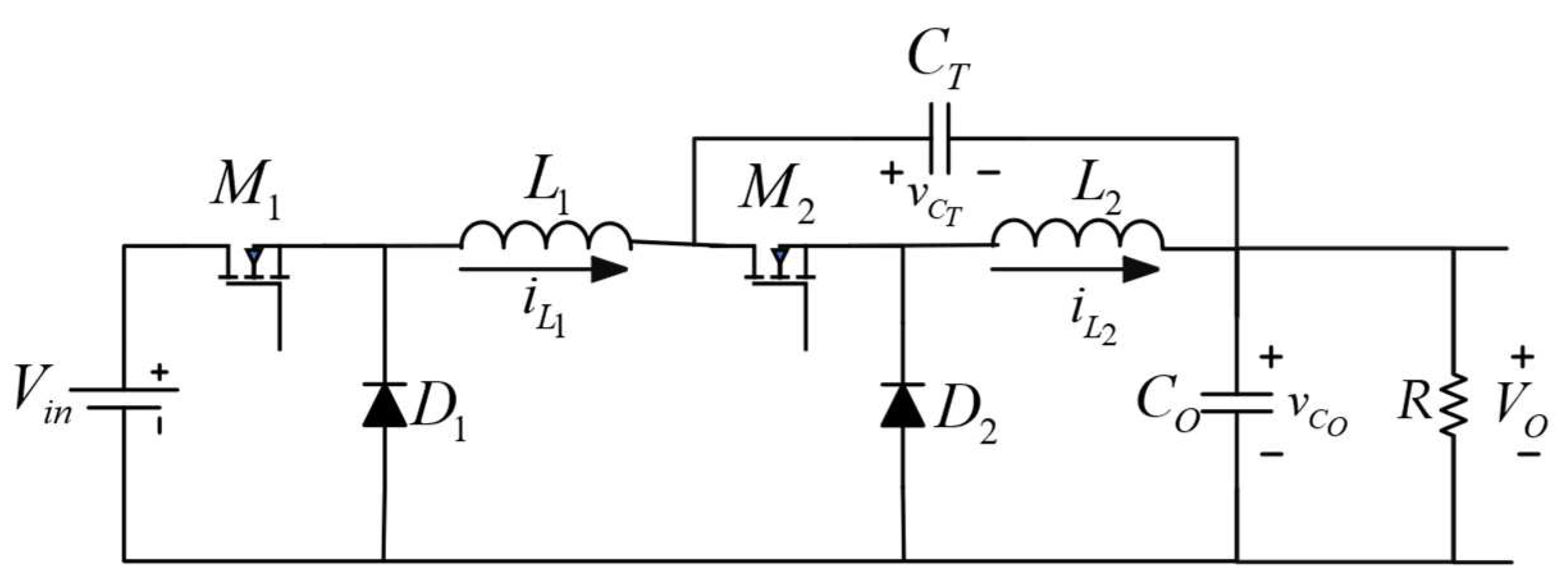
23]. When this principle is used, power efficiency is increased by providing a direct path to the load. The above translates into an improvement while maintaining the conversion capacity of the QBC. Several topologies based on this principle have been reported in the open literature. However, many still need to be studied in detail. For example, the quadratic-based step-down converter scheme described in [
24] is shown in
Figure 2, in which
represents the input voltage and
the output voltage. The transfer capacitor is represented by
and the output capacitor by
. The inductor of the first stage is
and the inductor of the second stage is
. The MOSFETs
and
are the active switches operating simultaneously,
and
are the diodes, and
stands for the load.
This topology has the advantage that both active switches operate with the same duty cycle, substantially facilitating the design and implementation of the MOSFET driver circuit. After the steady-state expressions and the dynamic models have been obtained, an analysis by linearization and control methods still needs to be carried out. As mentioned, one of the major problems of the conventional buck converter is the pulsating input current; this represents a drawback for many applications of power sources [
25].
Another problem in these converters is the strong electromagnetic interference (EMI) due to pulsating input current and the switching action of the semiconductor devices. An LC input filter can be placed between the power source and the switching converter to preserve the integrity of the input power. However, it is well-known that adding an LC filter to the input port may cause closed-loop instability [
26], leading to the need to add damping to the filter. This problem can be approached from an impedance viewpoint.
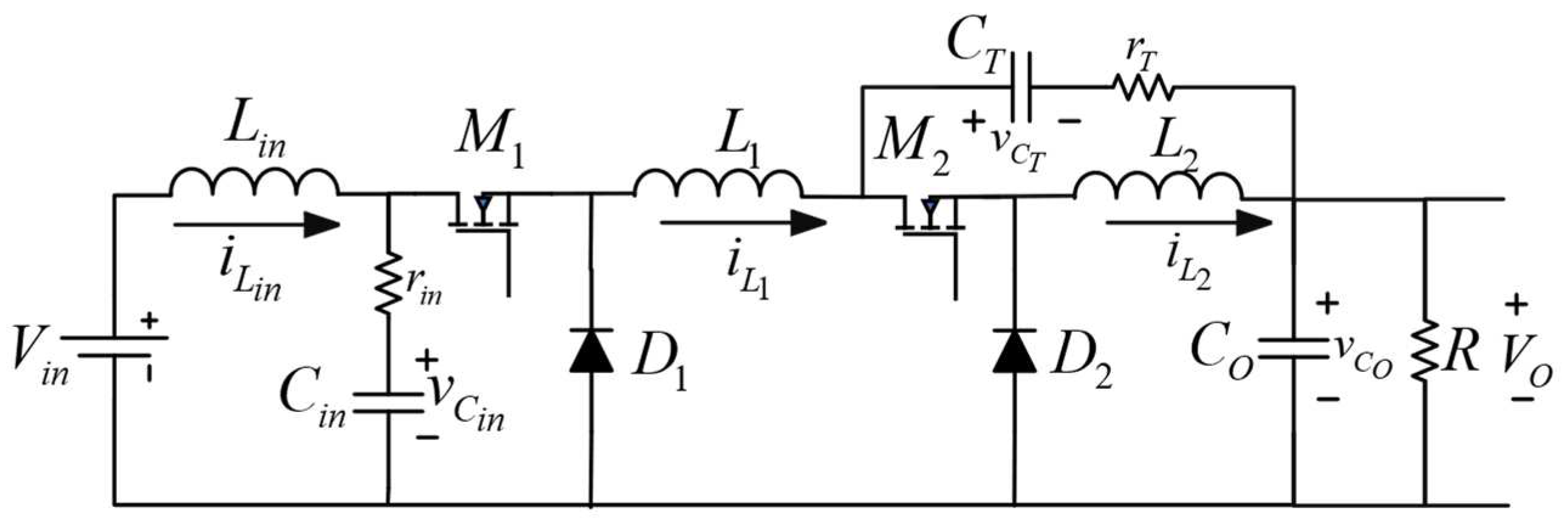
This paper aims to give general insight into the mechanisms of designing a switching regulator using a quadratic-based step-down converter combined with an input filter (QCIF) [
27] and to find simple and easy-to-use expressions for the proper selection of the parameters of the converter as well of the robust controller. In practice, the stability of a mathematical model is insufficient to guarantee acceptable system performance or even to guarantee the stability of the physical system that the model represents. Therefore, there is a need to determine how far the system is from instability. This degree of stability is known as relative stability. The resulting bandwidth is determined mainly by the converter. Also, the dynamics of the converter will be independent of the output load. The benefit of the approach is its simplicity, which can be seen immediately from the model, where the gains of the robust controller play an important role. This regulator provides a non-pulsating input current; thus, it is suitable as an interface between lithium-ion batteries and on-board applications. The paper is organized as follows. The relationships that allow fair values of the converter’s electric elements and stress voltage on switching devices are shown in
Section 2. A detailed analysis of the converter dynamics is given in
Section 3, where the equivalent series resistor (ESR) of the capacitor filter is added. The bilinear piecewise and linearized models are also derived, as well as an analysis of the effect of the input filter on the dynamics of the switching DC-DC converter and the control performance. The procedure for controller design is given in
Section 4 and
Section 5 shows test results in the time and frequency domains for a laboratory prototype with an output power capacity of 300 W. Finally, some conclusions are discussed in
Section 6.
3. Dynamic Analysis and Modelling of the QCIF
A model is obtained for each case to carry out a comparative study of the behavior of QCIF without and with the effect of ESR of the capacitors and inductors. To start with, a binary commutation function “
q” is defined to represent the dynamic of QCIF by a bilinear piecewise model. The commutation function takes the values 1 and 0 when
and
are ON and OFF, respectively. As a result, the set of equations corresponding to the inductor currents and capacitor voltages are shown in Equation (17) without the effect of ESR and Equation (18) with the effect of ESR:
It is well-known that high-frequency switching DC/DC converters can be approximated by their corresponding low-frequency continuous model. By averaging the q function and the state-space equations of the bilinear piecewise model, the related time-average functions with the form:
are obtained. In this expression,
x ϵ R6 is the state vector,
is the input voltage,
Ā ϵ R6×6 is a matrix,
ϵ R6 is the input vector, and
d(t) is the duty cycle. As can be seen, the matrix and the input vector are influenced by the duty cycle
d, so the set of equations is nonlinear.
By applying linearization techniques to nonlinear models, it is possible to describe the behavior of the converter. These models are linearized around the operating point corresponding to the steady-state values given by (1) to (6). The procedure to derive it is as follows. The input voltage, control signal, and six state variables are divided into two parts: the nominal average values, which are denoted by upper-case letters, and variations of their nominal operating point, which are denoted by lower case with a superscript “
”.
Then, the Equation (19) are rewrite in terms of the disturbed variables of Equation (20). The products of disturbance are not considered, since these are of second order. Finally in these equations, the values of the constant parameters are substituted by the nominal values of variables. The linear models without Equation (21) and with Equation (22) of the ESR of capacitors and inductors are obtained:
Based on the resulting linear models, the Laplace transforms are applied to analyze the dynamic behavior of the QCIF. This analysis mainly focuses on the transfer function
to determine the effect that the electric elements and ESR of the input filter capacitor have on the dynamic behavior of the QCIF and its output voltage. The resulting transfer function has the form:
where
ai and b
i with
i = 0…5 are the denominator and numerator polynomial coefficients. The expressions for the coefficients are too large, so they are omitted here due to space limitations; however, numerical results are shown in
Section 5.
The converter is stable and has non-minimum phase behavior; however, if the ESR of the capacitor input filter is added to the model, the coefficients b5, b3, and b1 become positive, which reduces the number of zeros on the right-hand side (RHS) of the s-plane. Furthermore, in physical applications, this characteristic can exhibit different values depending on the dielectric used in the capacitor by the manufacturer.
Despite this change, the transfer function
has non-minimum phase behavior because it continues to have zeros on the right-hand side (RHS) of the s-plane. For this reason, it is very difficult to achieve good closed-loop performance with only the voltage loop due to resonant peaks and abrupt phase changes [
28]. The transfer function
was also obtained:
It has the same poles as
but all its zeros are located in the LHS of the plane, thus it has minimal phase behavior. For this reason,
is a variable to consider when implementing a control system. In
Section 5, the numerical results are shown.
Finally, it is necessary to design the input filter to carry out an adequate design of the converter. The criterion is that it has to satisfy the following inequality [
26]:
where
Zf (s) is the output impedance of the input filter, and
ZC(s) is the input impedance of the converter. Their corresponding values are computed by:
where
The expression of the input impedance of the converter is obtained from the transfer function input voltage to input current
[
26] obtained from the state-space average linear model of QBC without filter, shown in
Figure 2, in which the input current of the converter is given by
.
Therefore, attention should be taken to satisfy the inequalities given in Equation (25). Once the impedance of the input filter has been ensured, the controller for the QCIF can be designed.
4. Controller Design for the Converter QCIF
The controller must efficiently mitigate the voltage changes in the output produced by the operational conditions, for example, changes in input source voltage and output load. When lithium-ion batteries are used, they exhibit voltage variations up to 15% of their nominal value. These variations depend on some factors: charging state, operating temperature, and nominal voltage, among others [
7,
29,
30]. Therefore, the controller should also compensate for the parametric uncertainties and nonlinearities presented by the QCIF. The two primary control approaches are voltage-mode control and current-mode control. The latter exhibits advantages over the voltage-mode control because sensing the current of the input inductor improves the transient response and protects against current overloads of the input power.
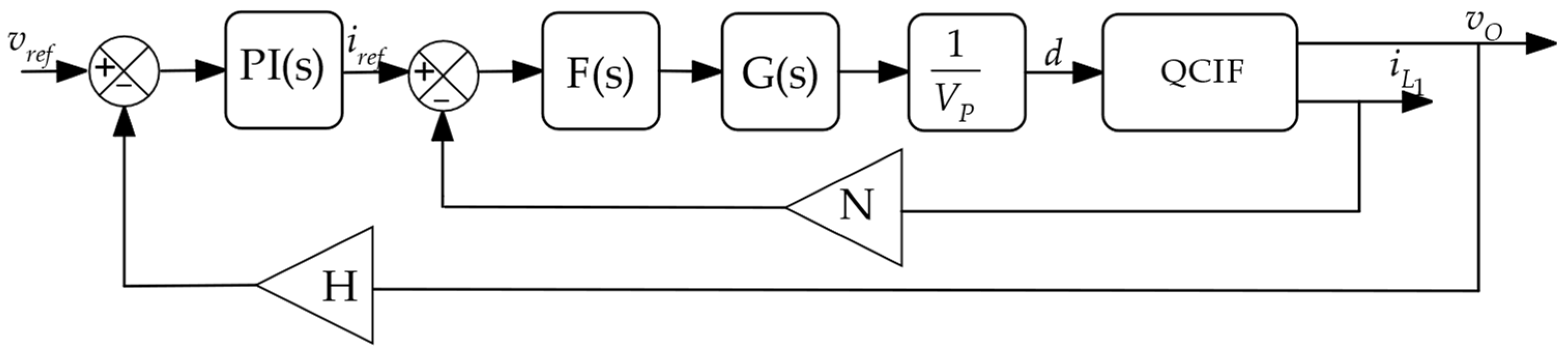
As mentioned in the above section, the stability is quite difficult to achieve when the transfer function
has RHS zeros. Moreover, selecting the inductor current that will be used for the internal loop is crucial from performance and implementation viewpoints. It was shown the transfer function first-stage inductor-to-duty cycle of the converter has minimum phase behavior, so it is appropriate for the internal current loop. Furthermore, this selection is appropriate to design the control loop with the highest gain and bandwidth; thus, the advantages of current-mode control are ensured. The block diagram for the control scheme is shown in
Figure 6, where V
ramp is a ramp waveform, which is compared with the control signal. A low-pass filter F(s) has a high-frequency pole, a high-gain compensator G(s) is added in the internal current loop,
is the desired voltage, N and H are the current and voltage sensor gains, and PI is the controller of the external voltage loop.
The control system design criteria are based on the loop-shaping technique. The following conditions should be satisfied for good performance of the switching regulator:
To reduce the sensitivity, the slope at the crossover frequency of the voltage loop gain must be approximately −20 dB/dec
For voltage regulation, the voltage loop gain should be high at low frequencies and low at high frequencies
For better speed response, the bandwidth should be large.
For robustness, good gain and phase margins are required.
The above conditions should be satisfied with the two control loops of the current-mode control; however, the PI-controller of the outer voltage loop plays an important role. The pole of PI-controller helps for voltage regulation and robustness. The zero of the PI-controller helps to reduce sensitivity and better speed response. The gain and phase margins should be positive if a closed-loop system is stable. In general, gain margins of 2–10 dB and phase margins of 30–60 degrees are desirable tradeoffs between bandwidth and stability in the closed-loop system design.
The procedure to design each loop, select the appropriate value of gains, and therefore choose the components of the controller circuit, are described below:
4.1. Internal Current Loop Design
At first, the internal loop, or current loop, is designed. It produces a faster transient response and, as noted in
Figure 6, consists of low-pass filter F(s) and a high-gain compensator G(s), with the following transfer functions:
respectively, where
is the location of the compensator zero whose value is given by
It must be placed at a frequency lower than that at which the LC filters produced naturally by the inductors and capacitors of the converter are located. Therefore, in practice is placed at least a decade below half the switching frequency of the converter, thus, the value of the resistor
and capacitor
can be calculated. The gain
of the compensator is given by
, and it has to satisfy the following inequality:
Thus, from this expression, it is possible to calculate the value of .
To provide noise immunity from the inductor current, the high-frequency pole of F(s) is placed at a frequency equal to or above half the switching frequency and can be computed by . From this expression, the capacitor can be calculated.
Thus, the control law is given by:
4.2. External Voltage Loop Design
Once the internal loop has been tuned, the external or voltage loop of the controller, is designed. It is composed of a voltage sensor with a gain H and a PI controller with a transfer function given by:
where
and
are the integral time in seconds given by
and proportional gain given by
respectively. The purpose of
is to provide a high gain to the controller at low frequencies; thus, the value of resistor
and capacitor
must be selected such that
is placed at least one decade below the converter switching frequency. The gain is set to obtain the appropriate gain and phase margins of the voltage loop by the expression
This gain is adjusted in the controller circuit by RFC/R1C. It is important to notice that expressions (30) and (33) provide a first approximation of internal and external loop controller gains; subsequently, an iterative tuning process has to be carried out to guarantee the appropriate robust stability of the regulator.
The expression of this loop, in the physical regulator is given by:
The electrical circuit of the proposed scheme controller for the QCIF can be implemented as depicted in
Figure 7. A flow chart showing the steps that must be performed to design, calculate, implement and experimentally verify the performance of the switching regulator based on the pro-posed converter model is depicted in
Figure 8.
5. Experimental Results
A QCIF was built in the laboratory to validate the theoretical development with the nominal conditions for the on-board converter of a hybrid electric vehicle: an input voltage of 48V, an output voltage of 12 V, and an output power of 300 W. The parameters of the converter are given in
Table 1, in which the duty cycle to be used is defined from the relationship between the output and the input voltage given by
. Because the switching frequency is a factor to consider in the design of the inductors to be used according to the relationships given by Equations (7)–(9), there should be an adequate relationship between the size of the inductor and the current that flows through it, determined by the power handled. The switching frequency of the converter should be greater than 20 kHz to prevent noise from being captured by the human ear.
The corresponding values of the elements are given in
Table 2. MOSFET elements with low on-state resistance, high current handling capacity, and reduced drain-source voltage are selected as active switches. In the case of passive switches, Schottky-type di-odes were used due to their low forward voltage drop, minimal switching losses, low voltage peak magnitudes, as well as ultra-fast recovery. The current and voltage characteristics of the devices are given in
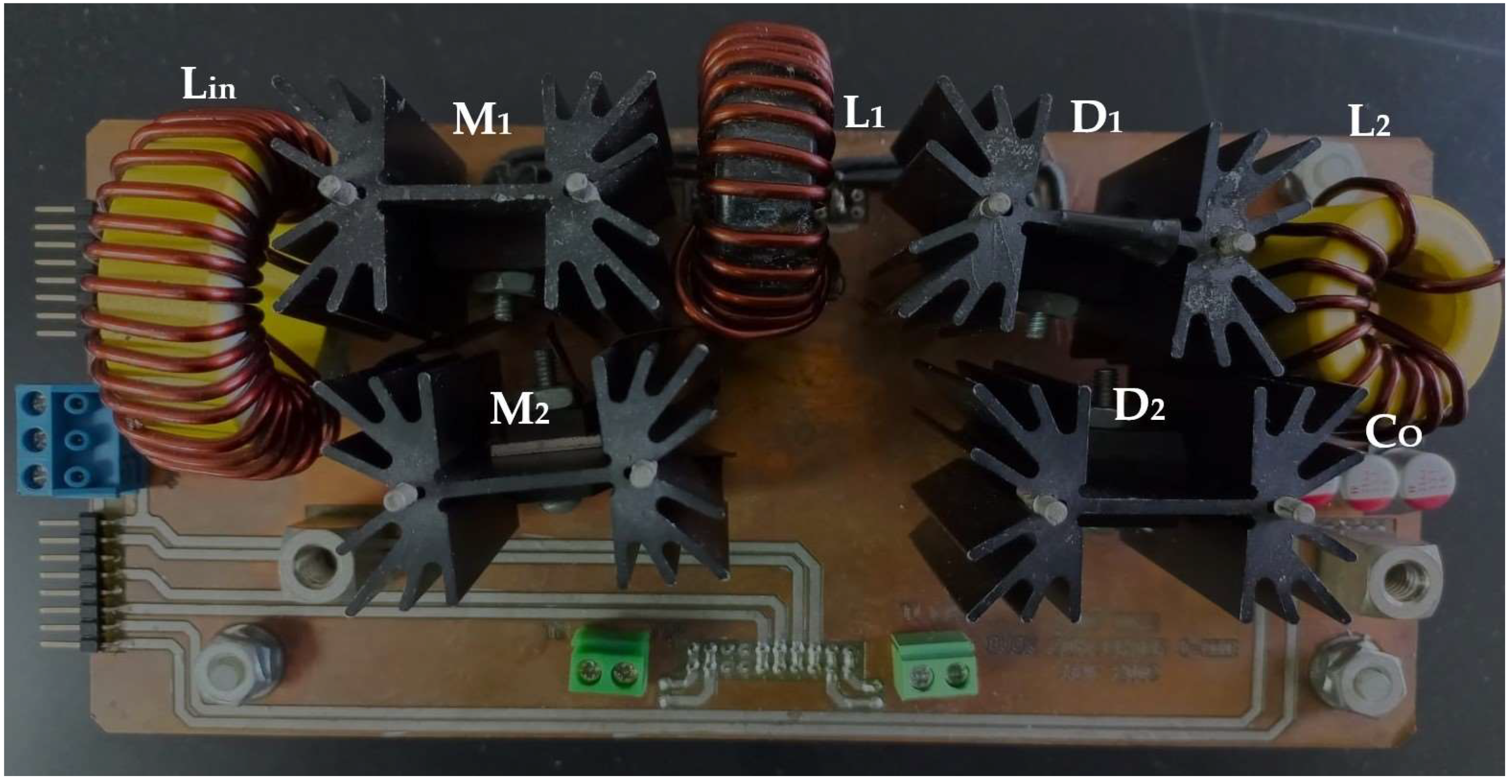
Table 2. A photo of the prototype is depicted in
Figure 9.
The transfer functions
and
were calculated numerically by substituting the values of the components of the QCFI from
Table 2 into the linear models of the converter without and with ESR given by expressions (22) and (23). These transfer functions were obtained using the ss2tf command of the Matlab
® software for ease. Subsequently, the zeros and poles of each transfer function were obtained, which are shown in
Table 3. As can be seen, the effect of ESR reduces the number of zeros of the transfer function
on the right-hand side (RHS) of the s-plane, and produces only zeros on the left-hand side of transfer function
, making the first-inductor current, suitable to be fed back into the current loop.
5.1. Open Loop Test Results
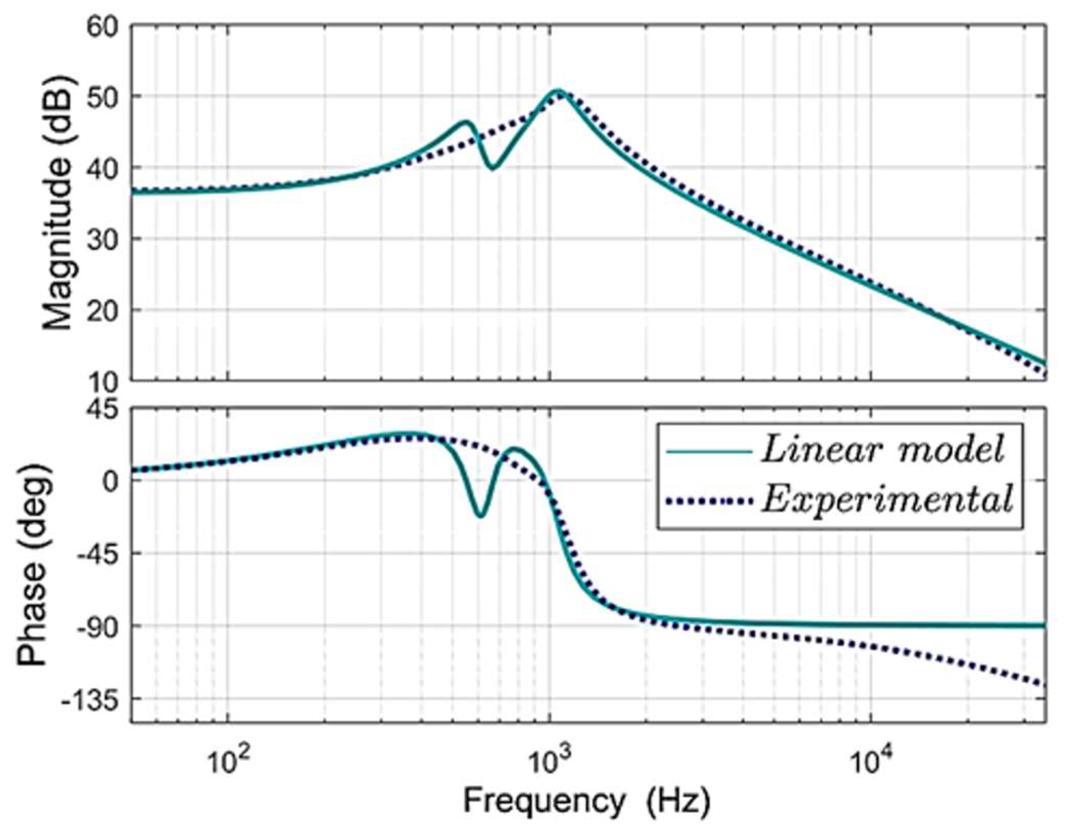
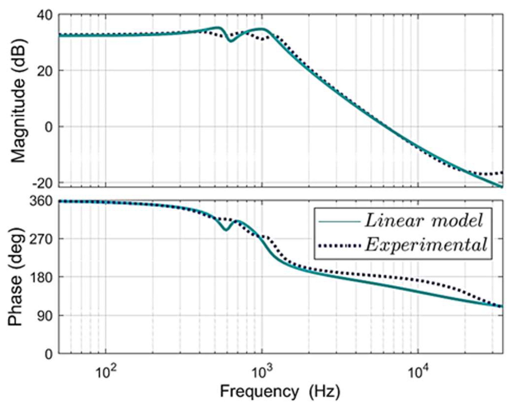
The proposed theoretical models of QCFI were validated in the laboratory using the frequency response Analyzer 300 AP. The theoretical frequency response of the transfer function of the first inductor current-to-duty cycle is compared with the corresponding experimental and shown in
Figure 10.
A high damping can be observed in the experimental response due to the parasitic resistances, as mentioned in
Section 3. The phase plot corresponds to a minimum phase transfer function suitable for designing a controller. The similarity between the two responses is remarkable. The theoretical and experimental frequency responses of the output voltage–to–duty cycle are shown in
Figure 11. The significant change in phase shows the existence of right-hand zeros in the transfer function. Both plots are very close. The proposed model accurately predicts the actual behavior of the QCIF and allows the model to be validated through the experimental frequency response. These models can be used to design a robust controller.
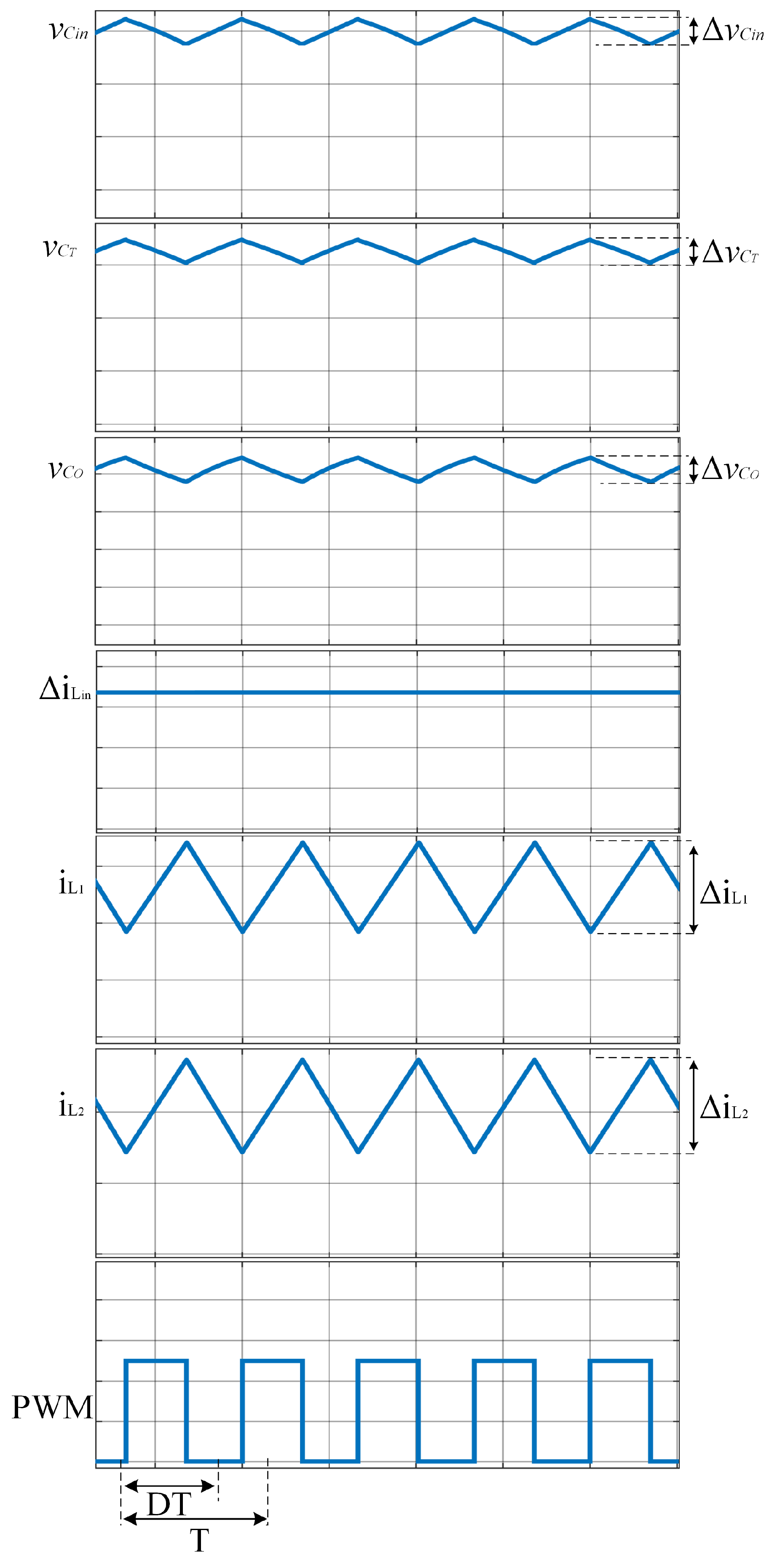
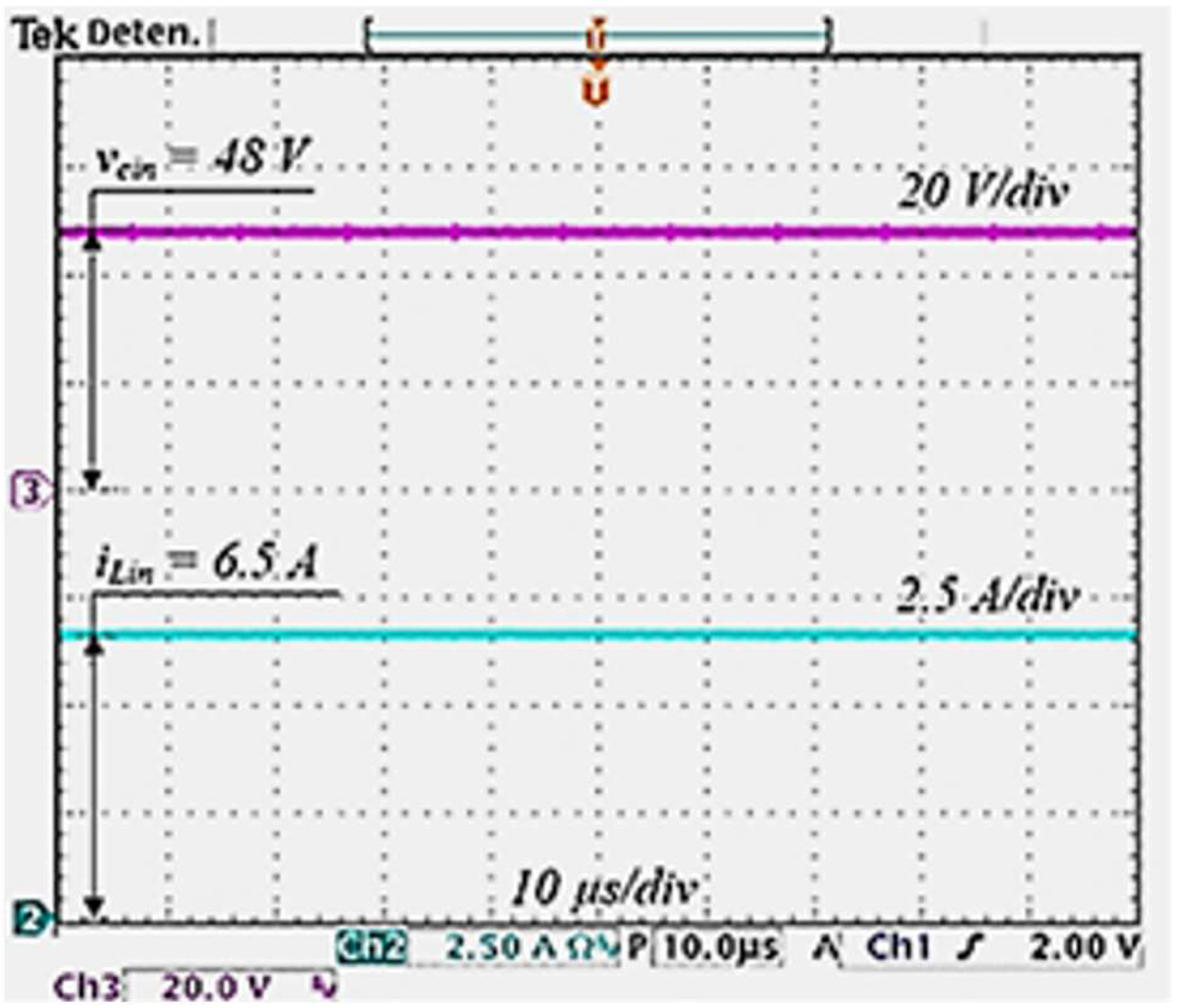
The first tests were taken in an open loop by adjusting the duty ratio to 0.5 to obtain the nominal operation. The inductor current and capacitor voltage of the input filter are shown in
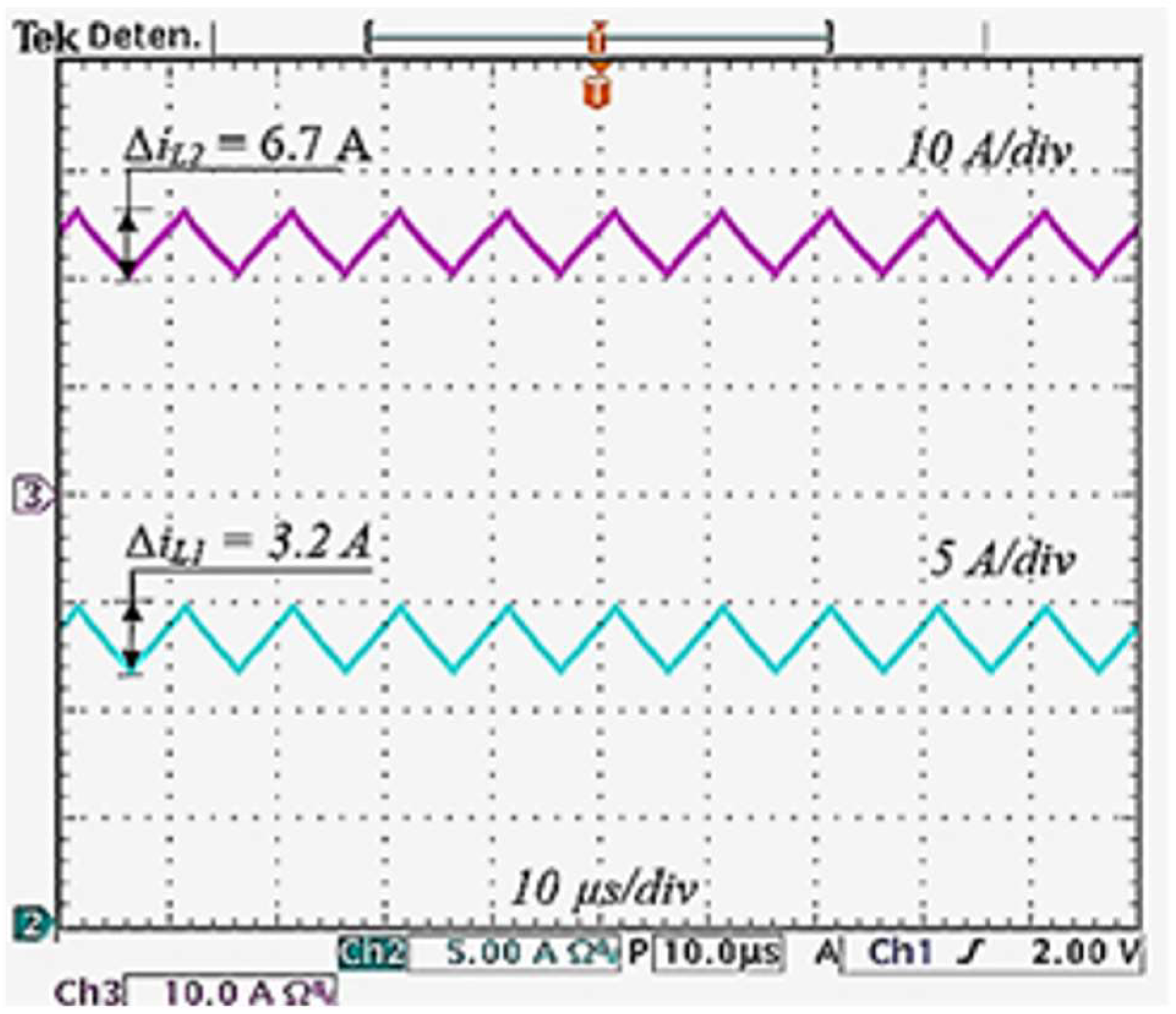
Figure 12; as can be seen, the input current to the converter has a value of approximately 6.5 A and does not have a pulsating waveform. This is suitable for processing energy from lithium-ion batteries. The current flowing through inductors
and
are depicted in
Figure 13; these signals were obtained using the Tektronix TCPA AC/DC series current measurement probes. The experimental waveforms have a sawtooth form, as predicted. The capacitor voltages
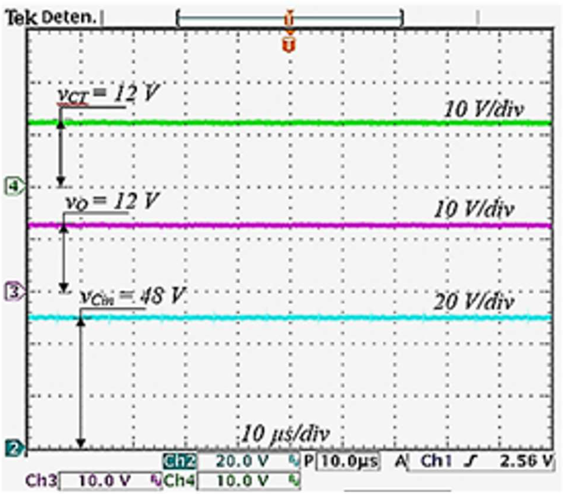
,
, and
are depicted in
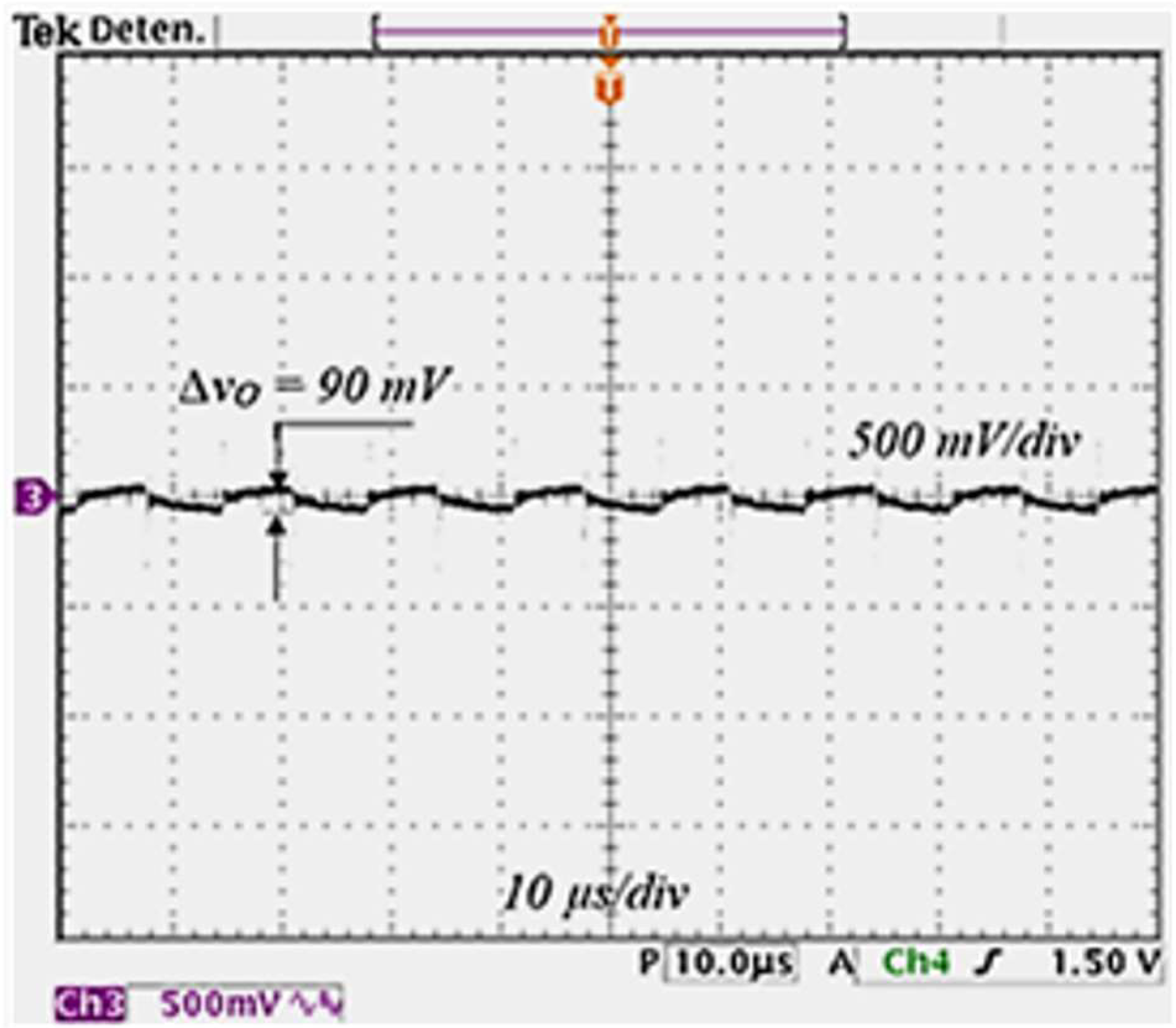
Figure 14. The voltages in the transfer capacitor and the output voltage have a value of 12 V voltage, as predicted. To appreciate the ripple in the output voltage, a zoom is obtained and shown in
Figure 15. The resulting ripple is about 90 mV, where the ESR effect of the output capacitor can be noticed. Finally, a summary of the ripples obtained analytically and experimentally is shown in
Table 4.
The behavior of the QCIF was examined in open loop to determine how step changes in load are reflected in the output voltage. The above was done by connecting an extra load in parallel to the nominal load, as shown in
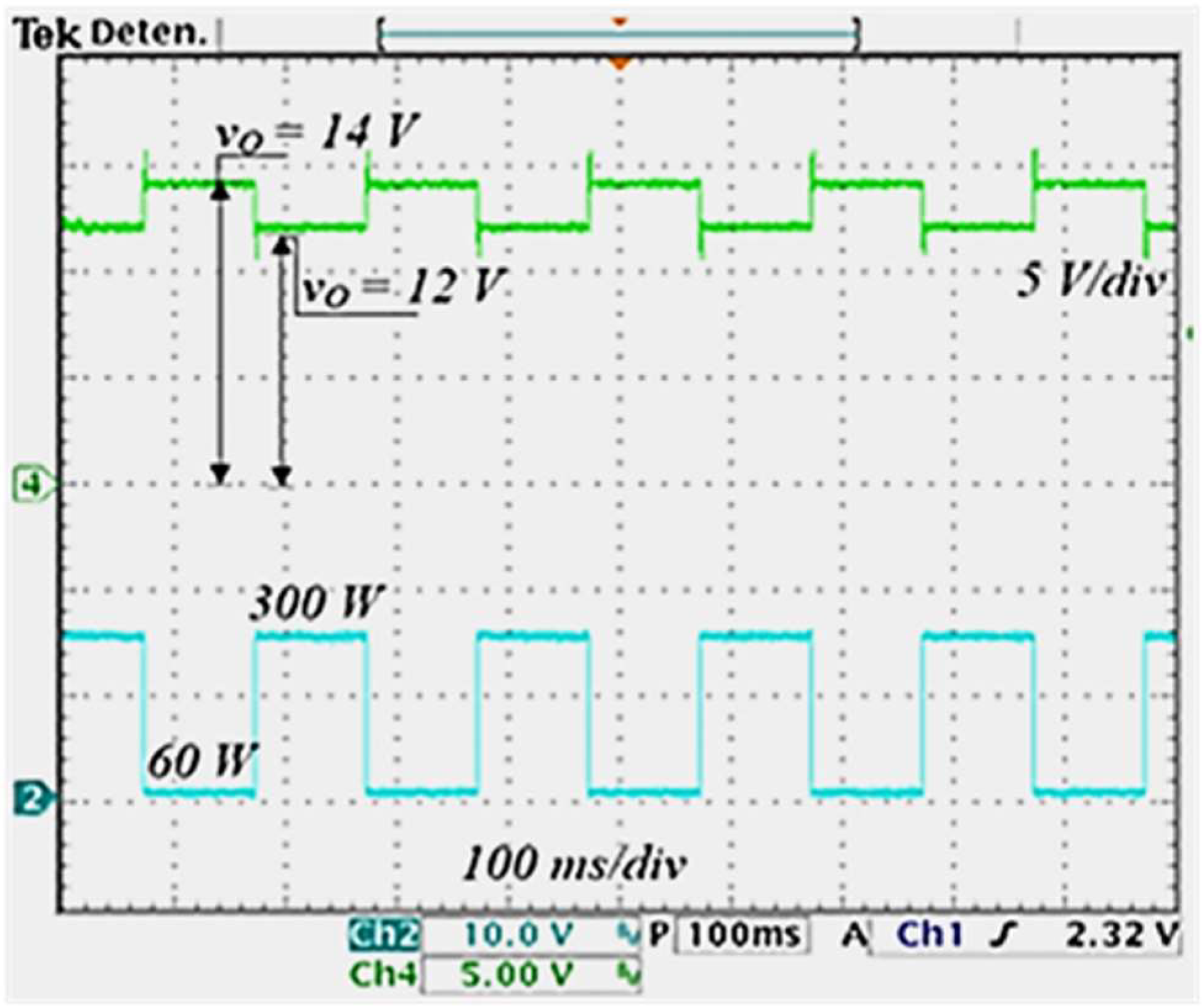
Figure 7. Then, a square signal was applied to MOSFET M at a frequency of 5 Hz. The load demands a current of 25 A when the MOSFET is ON and 5 A when it is OFF. The above represents a power consumption of 300 W (100% of rated output power) and 60 W (20% of rated output power). The output voltage response to these load variations is shown in
Figure 16. As can be seen, the output voltage reaches 14 V.
The efficiency of the converter at the rated output power of 300 W is defined as
. This value was obtained using the voltage and current data shown in
Figure 12,
Figure 13 and
Figure 14. The resulting efficiency of the QCIF is about 91%. However, when SiC or GaN power MOSFETs are used, the efficiency can be improved since they have lower on-resistances and better performance [
31]. Efficiencies of quadratic converters with different nominal powers reported in the open literature are shown in
Table 5.
5.2. Closed-Loop Test Results
The control scheme applied to the QCIF was designed according to the criteria mentioned in
Section 4. The regulator values are shown in
Table 6. The gain
H for the voltage sensor was implemented in the laboratory with a voltage divider. A Hall Effect current transducer was used to sense the first inductor current, specifically the LA-55P model from the LEM company.
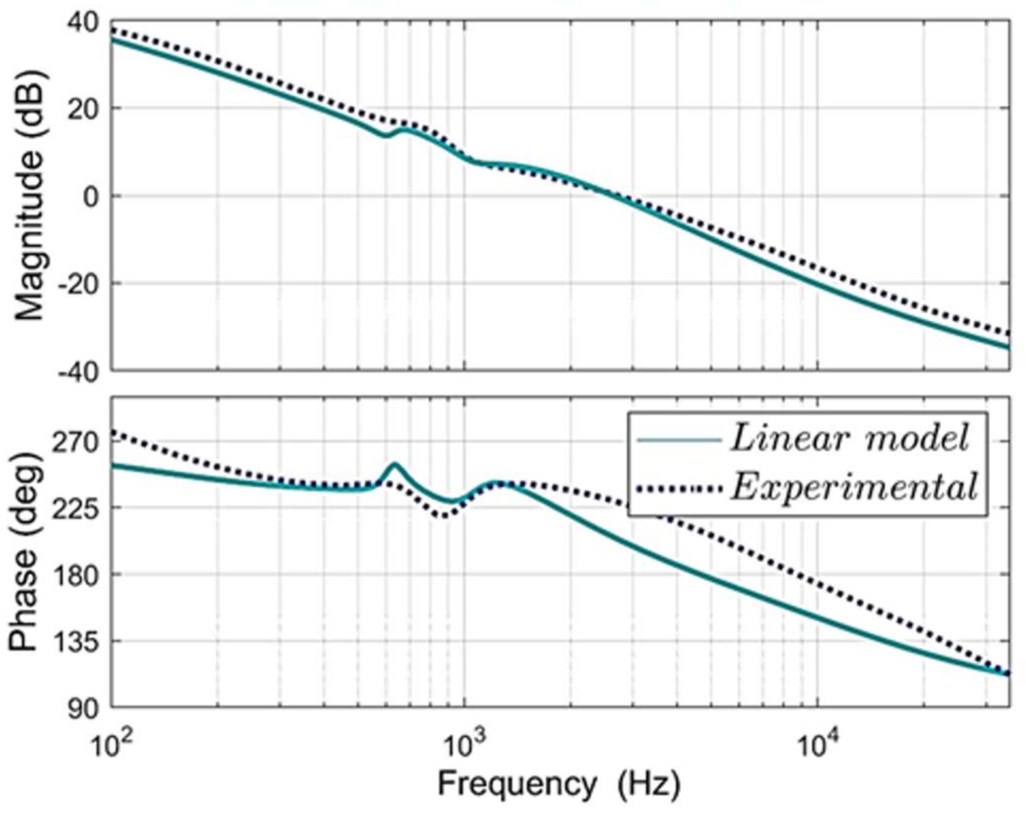
The performance when the controller is enabled was analyzed in time and frequency domains. A comparison between the experimental closed-loop frequency response and the closed-loop linear model Bode plot is shown in
Figure 17.
For both cases, the PI controller dominates the loop gain at low frequencies and has a slope of approximately 20 dB/dec at the crossover frequency. When the linear model is used, the loop gain has a 2.5 kHz bandwidth and phase and gain margins of 28 degrees and 9.5 dB, respectively. Furthermore, the response of the laboratory prototype has a bandwidth of 3.7 kHz; therefore, the regulator has a good response speed. The phase and gain margins are 38 degrees and 12 dB, respectively; thus, robust stability of the regulator is ensured.
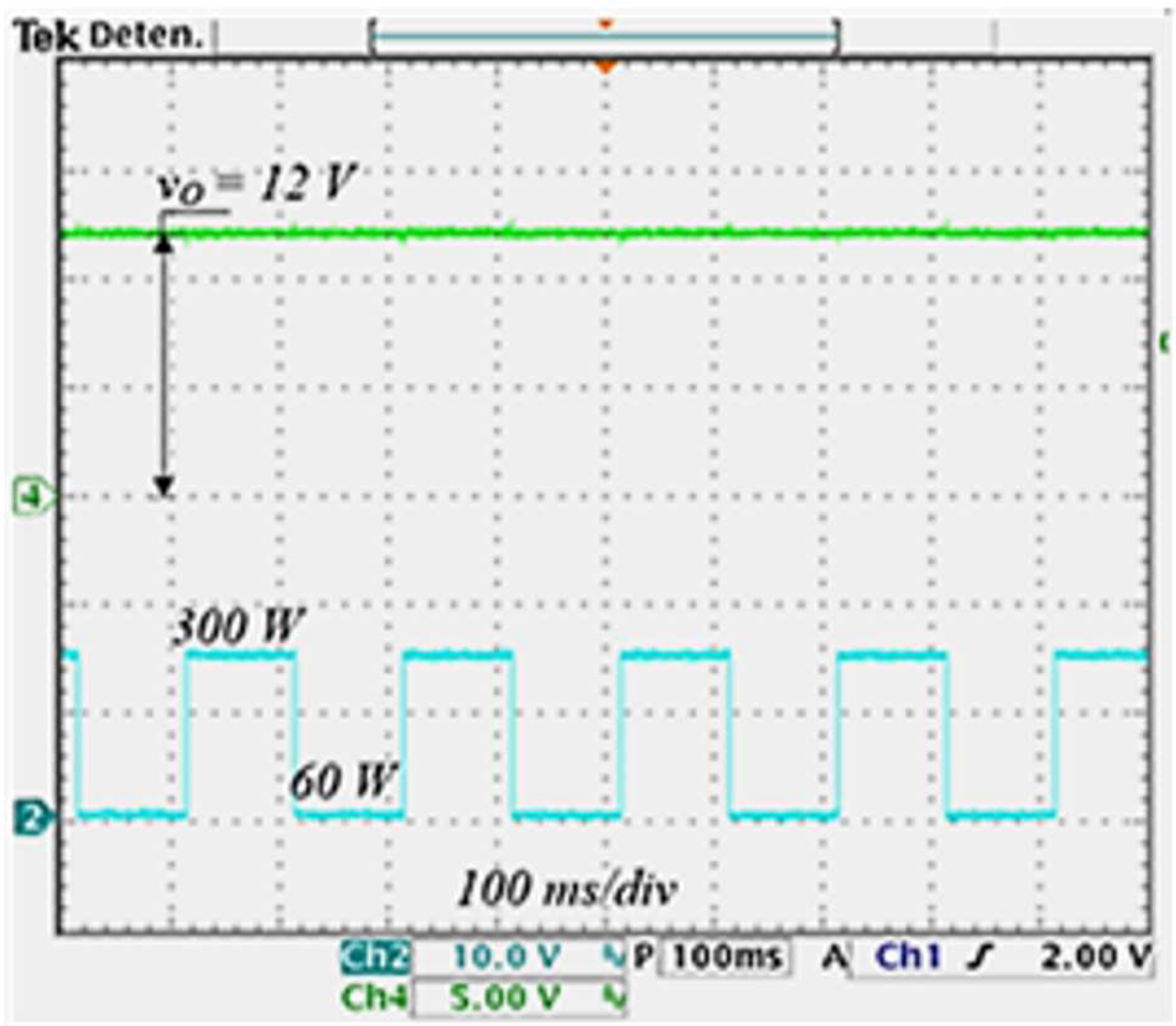
With the controller enabled, the same step load changes used in the open loop were now applied to QCIF for the time domain test. The experimental response is depicted in
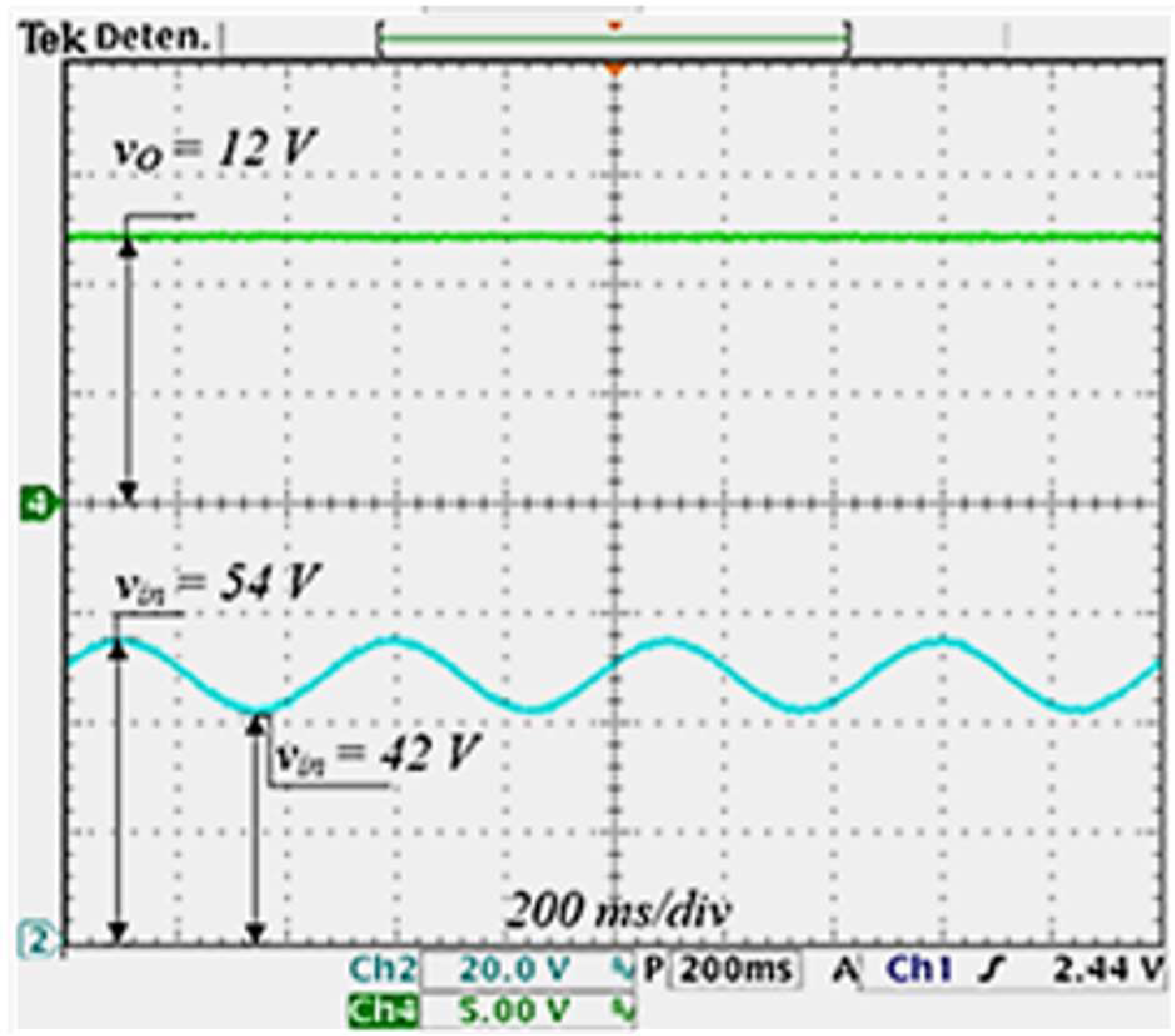
Figure 18. Additionally, experimental tests were performed for variations in the input voltage from 40 V to 53 V, corresponding to the voltage variations that a nominal 48 V lithium-ion battery can reach. These variations were injected sinusoidally at 2 Hz. The behavior of the output voltage for these variations is shown in
Figure 19. As can be seen, no voltage variation appears when load and input voltage changes are applied because the good characteristics were achieved in the control loop design. The resulting bandwidth improves the response speed to changes in the load. In addition, the slope at the crossover frequency of the voltage loop gain indicates good behavior of the sensibility function, and the gain and phase margins improve robustness.
With the idea that the proposed switching regulator could be integrated as a module to be connected to the on-board equipment, the present work implemented the controller using an analog circuit consisting of two operational amplifiers, resistors, and capacitors. The controller is very compact and simple. However, the proposed controller could be implemented digitally using a programmable microcontroller. In this case, it is possible to incorporate other techniques to design the controller used to implement the current-mode control scheme. For example, controller optimization and efficiency methods, such as the one proposed in [
35], stand out. It combines a fractional-order proportional-integral-derivative (FOPID) controller with a metaheuristic algorithm, an improved version of the Hunger Games search, as well as the help of the Nelder-Mead Method and a random learning mechanism, to optimize its tuning. Although this scheme is implemented in a one-stage step-down converter, which presents a minimal phase dynamic response so that it can be controlled in a voltage-mode scheme, unlike the proposed converter, it does open the interest of adapting this method to the current-mode control scheme.


