Abstract
As non-isolated step-up and step-down DC–DC converters are at present widely used in various fields, this review will summarize and introduce non-isolated step-up and step-down DC–DC converters in various aspects. First of all, the origin and development of power electronics technology and the generation and principle of certain basic non-isolated step-up and step-down DC–DC converters are briefly stated. Subsequently, according to their different characteristics, including whether they are unidirectional or bidirectional, voltage-fed or current-fed, or hard-switching or soft-switching, the review will classify them and analyze their advantages and disadvantages. Meanwhile, in order to change the voltage gains of the DC–DC converters, different voltage change techniques are applied to them. The review will elaborate on the four technologies (switched capacitors, voltage multipliers, switched inductors and different ways of connecting), providing examples and analyzing the topologies in which they are applied, before summarizing the advantages and disadvantages of these techniques. Finally, this review will describe the specific applications of non-isolated step-up and step-down DC–DC converters and the reasons behind their ubiquity and popularity. Although the performances of current DC–DC converter topologies are good, there continues to be increasing demand, an updating of the topology structure, and improvements in terms of their performance. In the future, DC–DC converters will play a more important role in industrial production and people’s lives.
1. Introduction
From the Second Industrial Revolution until now, electric energy has been important in industrial production and normal people’s lives. In 1882, T. Edison invented the first DC distribution system. However, at that time, the problem was how power plants could transmit electricity over a long distance at a low cost. Electricity must be transmitted efficiently over a long distance under the condition of high voltage. In 1885, AC transmission was introduced with the invention of the transformer, which can increase the voltage and deal with the above problem well. However, transformers can only achieve AC–AC transformation at the same frequency. In addition, transformers’ energy losses, magnetic radiations, large volumes of copper, and high costs restrict their extensive use. In many applications, it is the hope that electric energy will be converted between AC and DC, between DC and DC, and even between different frequencies. In order to meet this demand, and with the development of and improvements in semiconductor switching technology, power electronics technology came into being [1,2,3].
As one of the four great transformation technologies of power electronics, DC–DC converters are the core of modern power conversion technology and are widely used in electrical power systems, communication systems, household appliances, industrial equipment, railways, aviation, and many other fields [1]. Among them, there are three basic structures: buck, boost, and buck–boost converters. A buck–boost converter is a combination of a buck converter and boost converter topology. It consists of inductors, capacitors, diodes, and semiconductor switches which can realize both voltage step-up and step-down from the input port to output port. When the duty cycle (D) is greater than 0.5, it operates in step-up mode. When the D is less than 0.5, it operates in step-down mode. The traditional buck–boost converter has attracted much attention because of its advantages, including its high efficiency, low cost, simple structure, and simple control. Its disadvantages consist of a limited voltage gain range, negative output voltage, and discontinuous input and output current [4]. In theory, as the D approaches 0 or 1, the output voltage should approach 0 or infinity. Nevertheless, in practice, due to the loss of the power switching transistor and the limitations of diode technology, the output demand will not be met at the extreme duty cycle.
At present, due to the consumption of fossil fuels, the impact on the environment and climate, and the low pollution and high efficiency of renewable energy sources (RESs), the use of RES has become popular throughout the world. Solar photovoltaic (PV) technologies, uninterruptible power supplies, wind turbines, and fuel cells are also increasingly popular. The output voltage level of RESs are low and require wide gain and high efficiency DC–DC converters. However, traditional buck–boost converters cannot be applied in this way [5,6]. Several non-isolated converters, such as Cuk, SEPIC, and Zeta converters, which are improved topologies based on buck–boost converters, are also unsuitable in such a context. Therefore, it is urgent a way to solve this problem is found. There are two ways to achieve this demand. One is to use transformers and coupling inductors. However, transformers have shortcomings such as leakage induction, electromagnetic loss, large volumes, high costs, and small power densities, so that, in addition to the need for electrical isolation, the second solution has generally been pursued: the study and design of new non-isolated DC–DC topologies. The different non-isolated buck–boost converter topologies have their specific characteristics and should be selected and classified based on their applications and requirements, such as: unidirectional or bidirectional, voltage-fed or current-fed, and hard switched or soft switched [7].
Luo converters can obtain higher voltage gains by using voltage lift technology, but their topological complexity, cost, volumes, and losses are increased. Their advantages can also be realized by cascading and interleaving, but their structure and control mode become more complex, and the efficiency of cascade circuits is not high [1,8,9]. The switched capacitor (SC) technique can also generate new topologies, but there is the problem of their high-current transients. Voltage multipliers can also be used in buck–boost circuits to obtain higher or lower voltage requirements in a modular way. However, there are many defects associated with these, including a large number of elements, the high voltage stress of switches and diodes, large losses, and so on. Therefore, different applications require additional topologies using different techniques. Such techniques will therefore need to be analyzed.
In this review, a general description of the non-isolated buck–boost converter is provided. According to the different characteristics of the converter, its classification will be presented in Section 2. Additionally, techniques for achieving voltage lift, such as switched capacitor, voltage multiplier, switched inductor, and different ways of connecting, will be presented in Section 3. In Section 4, the application of these converters will be provided in detail. Finally, the paper will summarize the whole paper and look forward to the future development of converters.
2. Categories of Step-Up and Step-Down DC–DC Converters
2.1. Unidirectional and Bidirectional
According to the direction of power flow in the circuits, non-isolated buck–boost converters are divided into unidirectional and bidirectional converters. Unidirectional buck–boost converters, where power flows from one port to the other rather than to each other, are usually achieved with unidirectional semiconductor switches and diodes. The general structure is shown in Figure 1. Traditional buck–boost, Cuk, SEPIC, and Zeta converters are typical unidirectional buck–boost converters. A traditional buck–boost circuit is shown in Figure 2. Due to the diode’s one-way connectivity, the flow of current through it cannot be reversed, so power only flows in one direction. Bidirectional power flow can be realized to form a bidirectional buck–boost converter by replacing passive switches with active switches in unidirectional circuits. The general structure of such converters is shown in Figure 3. A traditional bidirectional buck–boost circuit, shown in Figure 4, has two active switches and allows for the bidirectional flow of power [10]. When the circuit operates in buck mode, switch S1 is on and S2 is off. The power flow from V2 to V1 is achieved by controlling S1 and the body diode of S2. When the circuit operates in boost mode, switch S1 is off and S2 is on. The power flow from V1 to V2 is achieved by controlling S2 and the body diode of S1. In practical applications, unidirectional buck–boost converters are generally used when there is no need for bidirectional power flow because they feature fewer active switches, lower cost, simpler control modes, and relatively small losses.
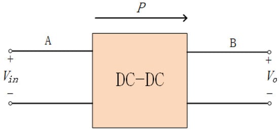
Figure 1.
Non-isolated unidirectional DC-DC converters.
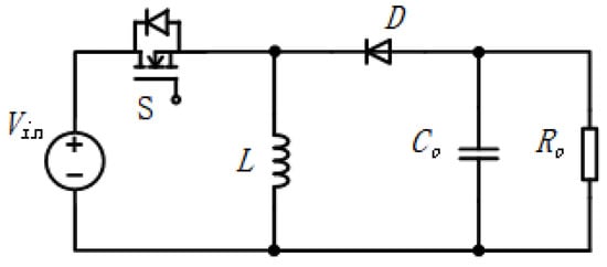
Figure 2.
Traditional buck-boost converter.
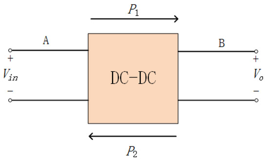
Figure 3.
Non-isolated bidirectional DC-DC converters.
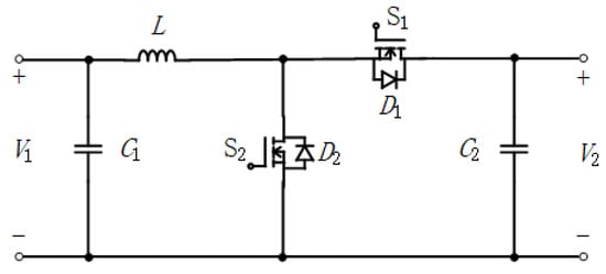
Figure 4.
Traditional bidirectional buck-boost converter.
Bidirectional buck–boost converters play an important role in PV power generation and distribution, electric vehicles, satellites, fuel cells, DC uninterruptible power systems, aerospace power systems, marine power supplies, DC microgrids, wind energy utilization, and other applications [11,12]. However, the topology of bidirectional buck–boost converters is different for different applications. There are many topologies of bidirectional buck–boost converters [13]. For example, in the application of renewable energy systems, the topology proposed in [14], as shown in Figure 5, has a simple structure and control mode as well as a wider voltage conversion range. The topology proposed in [15], as shown in Figure 6, has a simple structure and a high voltage gain. In addition, the input current is divided to the inductors, which leads to a smaller size as well as a large power density that can be used for battery charging and discharging. Bidirectional buck–boost converters can achieve bidirectional energy flow, so they generally use different power directions to achieve the step-up and step-down of voltage. For example, as indicated in [16] (with the topology proposed shown in Figure 7), by controlling the active switches, the circuit operates in boost mode in forward flow and step-down mode in reverse flow, which takes advantage of the topology and reduces the number of elements and the complexity as well as the cost of the circuit. A bidirectional buck–boost converter with a high gain, a continuous input and output current, and a low ripple was proposed in [12], as shown in Figure 8, with its efficiency being approximately 94.4% in charging mode. By controlling the active switch in the proposed topology, the circuit can realize the function of step-up and step-down voltage through the control of the D in the process of forward or reverse power input. The content is described in Table 1.
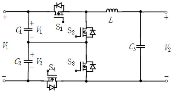
Figure 5.
A non-isolated bidirectional DC-DC converter in [14].
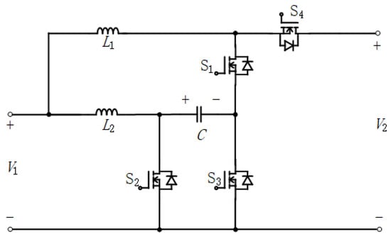
Figure 6.
A non-isolated bidirectional DC-DC converter in [15].
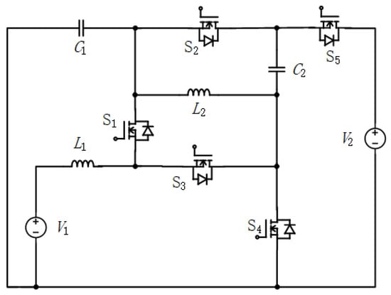
Figure 7.
A non-isolated bidirectional DC-DC converter in [16].
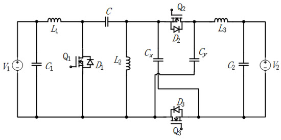
Figure 8.
A non-isolated bidirectional DC-DC converter in [12].

Table 1.
Voltage gain and other features in select converters.
2.2. Voltage-Fed and Current-Fed
According to the characteristics of the input source of non-isolated voltage converters, such converters can be divided into voltage-fed and current-fed converters [17]. In the case of voltage-fed converters, the input source is generally a constant voltage source, and a large capacitor is added at input port to simulate it. Because the voltage source is the main power source in nature, voltage-fed converters are widely used nowadays. However, there are also certain energy sources whose primary attribute is current, such as photovoltaic generators and superconductive magnetic energy storage (SMES) devices. These require current sources. In general, however, when used in series, large inductors and voltage sources are able to simulate the output of current sources [18,19,20].
The conversion between voltage-fed and current-fed converters can be completed by making use of duality transformation methods or adding input capacitors at the input terminals to meet the terminal constraints stipulated by the source. Concerning the first method, it is obvious that the on-time sub circuits of the voltage-fed converters would generate the off-time sub circuits of the relevant current-fed converters and vice versa. For example, a voltage-fed buck–boost circuit, as shown in Figure 9, can be converted into the current-fed buck–boost circuit shown in Figure 10. It is well known that the most common way to provide an interface between current sources in photovoltaic generators is to use a voltage-fed converter with input capacitors. Current-fed buck–boost power-stage converters are commonly used in series-connected distributed photovoltaic applications, where the output voltages are both step-up and step-down.
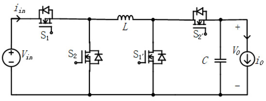
Figure 9.
A voltage-fed buck-boost converter.
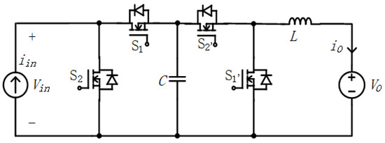
Figure 10.
A current-fed buck-boost converter.
2.3. Hard Switching and Soft Switching
Devices and machines that provide DC power require efficient DC–DC converters in the form of active switching in order to maximize the use of the energy provided. In the operation process of the converters, in order to make small volume converters of a light weight with low noise, it is necessary to increase the switching frequency. However, for hard-switching converters, a high switching frequency can result in high switching losses and electromagnetic interference (EMI), making them inefficient [21]. Therefore, in such cases, the switching frequency will be limited. In order to solve this problem, various soft-switching converters which take advantage of stray inductors and capacitors as part of a section of resonance circuits to achieve zero-voltage switching (ZVS) or zero-current switching (ZCS) are emerging [22].
According to the auxiliary circuit structure (whether there are auxiliary circuits or active devices), the soft-switching technologies of non-isolated DC–DC converters are divided into three categories: control-only technology (COT), non-auxiliary switch technology (NAST), and auxiliary switch technology (AST) [23]. COT does not use any auxiliary devices, and it is only through the adjustment of the circuit parameters and a change in the switching control method that soft switching is achieved. Its topology is relatively simple because it focuses on the control strategy. In order to reduce the switching losses of non-isolated DC–DC converters, the corresponding auxiliary circuits should be added to the circuit topology, which can be classified into NAST and AST, depending on whether the auxiliary circuit contains a controlled switch. NAST is also composed of quasi-resonant converters (QRCs), a passive snubber converter (PSC), and auxiliary commutation converters (ALCCs). Small inductors and capacitors connected to the switching elements in series or parallel are applied in QRCs to achieve ZCS or ZVS conditions. The topologies of QRC technologies are shown in Figure 11, among which (a) and (b) achieve ZCS and (c) and (d) achieve ZVS. This topology is used in buck–boost circuits [24], which implement ZVS. The PSC is a snubber network of capacitors, diodes, and inductors to realize ZCS or ZVS conditions. As shown in Figure 12a, that are several topologies in terms of PSC, with this structure being used in [25,26]. ALCCs achieve ZVS and ZCS conditions by generating an auxiliary current superposition between two semiconductor devices. This technology is used in bidirectional DC–DC converters [27]. AST consists of zero voltage transition converters (ZVTCs), zero current transition converters (ZCTCs), active resonant converters (active RCs), and active snubber converters (active SCs). Their structures are shown in Figure 12, where (b) and (c) are ZCTCs and ZVTCs, respectively, which are reflected in [28,29], respectively, and (d) and (e) are ASTs that can be used for SEPIC and Zeta circuits, respectively. An active SC structure, which was used in [30], is shown in Figure 12f. The switching devices in the converter adopt a partially resonant soft switch with a constant switching frequency. Therefore, the converter uses a partially resonant circuit to achieve soft switching (ZCS when on and ZVS when off). This method greatly reduces the power losses of the switching devices and improves the operational efficiency of the converters. Soft switching with active switches can also be used in bidirectional buck–boost converters, shown in Figure 13, which implement ZCS [31].
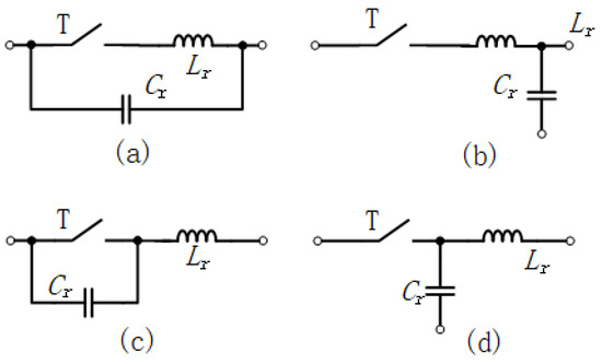
Figure 11.
Switching units of QRCs. (a,b) Achieving ZCS. (c,d) Achieving ZCS.
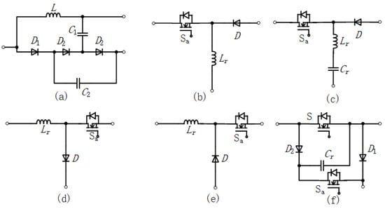
Figure 12.
Soft-switching circuits. (a) PSC. (b) ZVTs. (c) ZCTs. (d,e) AST. (f) Active SCs.
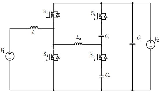
Figure 13.
A soft-switching bidirectional buck-boost converter.
A summary of the categories of step-up and step-down DC–DC converters is provided in Table 2.

Table 2.
Summary of categories of step-up and step-down DC-DC converters.
3. Different Step-Up and Step-Down Voltage Techniques
This section may be divided by subheadings. It should provide a concise and precise description of the experimental results, their interpretation, as well as the experimental conclusions that can be drawn.
In non-isolated converters, the voltage gain in the converters can be changed by four techniques, namely an SC, voltage multiplier, switched inductors, and different ways of connecting. The different techniques use different principles, so they can achieve different results. They have their own characteristics. The following is a detailed introduction of their principles, structures, and characteristics and examples used in the literature.
3.1. SC
The SC is a common method used to change voltage gain in buck–boost converters. The SC DC–DC structure, which is a modular structure consisting only of switches and capacitors, is also one of the most widely used and popular topologies in industrial and academic fields. It does not involve the storage and release of energy in the working process but only through the transfer of energy on the capacitor. Its advantages include its light weight, high efficiency, high power density, and easy modularization. Meanwhile, the serial-parallel SC converter has the advantages of high efficiency, simple control, and convenient power expansion, but it can only obtain integer multiples of voltage gain.
A basic charge pump (CP) circuit [7] is shown in Figure 14a. Switch 1 and 2 are turned on and off alternately. When switch 1 is on, the voltage on C1 reaches the input voltage Vin, and then 1 is off and 2 is on. The voltage across C2 is equal to the input voltage, and so on, and the output voltage is equal to the input voltage at the end. Doubler SCs can be obtained by transforming the basic CP circuit [32], as shown in Figure 14b. By alternating the switching of the switch, the output voltage is twice that of the input voltage, thus achieving the purpose of increasing the voltage. Not only can the input voltage be increased by two times, but the series-parallel topology can increase the output voltage further. As shown in Figure 14c, in the first stage, each capacitor is charged to the input voltage. In the second stage, these capacitors are connected in series so that the output voltage is three times that of the input voltage. A ladder SC, shown in Figure 14d, consists of two sets of capacitors that obtain different voltage gains by varying the input voltage nodes situated in the lower end of the capacitor ladder. The above are SC technologies that can only step-up voltage. The Fibonacci SC converter can realize both step-up voltage and step-down voltage. Its step-down voltage circuit is shown in Figure 15a, and its output voltage gain is one-fifth of the input voltage gain. Its step-up voltage circuit is shown in Figure 15b, and its output voltage is five times that of the input voltage, which requires a small number of capacitors, achieving small size requirements. Its magnification is a sequence (1,1,2,3,5,8…). Similarly, its magnification depends on the value of K, which starts at 0 and represents the number of capacitors. In our figure, K is four, so it has a magnification of five and a reduction of one-fifth [33]. The efficiency in step-down mode (98%) is higher than that in step-up mode (80%).
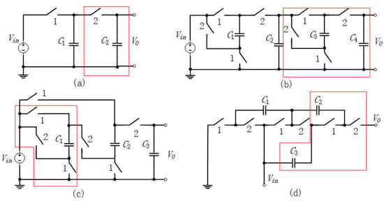
Figure 14.
Basic charge pump and switched capacitor circuits. (a) Basic charge pump. (b) Doubler. (c) Series parallel. (d) Ladder.
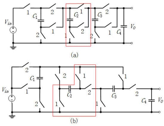
Figure 15.
Fibonacci. (a) A Fibonacci step-down converter. (b) A Fibonacci step-up converter.
An improved SC circuit based on a Cuk circuit, as proposed in [34], is shown in Figure 16. It is composed of many SC structures and Cuk circuits, which can step-up and step-down voltage. It also has a wider voltage gain range, lower voltage stress on SCs, and a continuous input current. It is also extensible and easy to modularize. When n is three, as the power changes, the efficiency varies from 92% to 97.2%. This SC can also be used to modify the Zeta circuit, with the efficiency varying from 93% to 97.2%. Its voltage gain is:
M = nD/(1 − D),

Figure 16.
A Cuk-derived step-up/down SC converter in [34].
Another SC similar to that in a previous paper was introduced [35], as shown in Figure 17. It can also be used in Cuk circuits and Zeta circuits due to the similarity of the structure. When n is three, as the power changes, the efficiency varies from 92% to 98% in the Cuk circuit and from 94% to 98% in the Zeta circuit, respectively. Of course, the input current in the Zeta circuit is discontinuous, and the other characteristics are basically the same. Moreover, the number of switching tubes in this new module is relatively small. The voltage gain is the same. As indicated in [36], this circuit can be used for high-voltage direct current (HVDC) systems due to its high gain and continuous input current. Its structure is shown in Figure 18. When n is 2, as power varies from 500 W to 3000 W, the efficiency varies between approximately 92% and 96% and its voltage gain is:
M = D(1 + D)(2 − D)/(1 − D),

Figure 17.
A Cuk-derived step-up/down SC converter in [35].
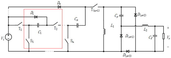
Figure 18.
A switched-capacitor-based DC-DC converter.
This method of changing the voltage gain of circuits is limited, as it requires more capacitors, switching tubes, and diodes, despite the circuit structure being simple and easy to modularize. Therefore, there are various techniques that can be used to change the voltage gain of a circuit. A summary of different step-up/down SC converters is provided in Table 3.

Table 3.
Review of different step-up/down SC converters in the review.
3.2. Voltage Multiplier
Voltage multiplier circuits are very common technologies in buck–boost converters, which have the advantages of a simple structure, easy modularization, high efficiency, wide range in terms of voltage gain, and low costs. Inserting these structures at different locations in the circuits of conventional buck–boost, Cuk, SEPIC, and Zeta converters changes the voltage gain.
Voltage multiplier circuits are generally composed of capacitors, diodes, and inductors. As shown in Figure 19, these multipliers can be classified into step-up and step-down multiplier structures and can be used in different step-up and step-down voltage circuits. Three kinds of step-up multiplier and two kinds of step-down multiplier, as well as their applicable basic converters, were introduced in [37,38], respectively. In addition to the structure shown in Figure 19a inserted in the front of the switch, they generally replace the combination of capacitors and diodes or inductors and diodes in the circuit to achieve a new circuit topology. The converters that they are applied to and the voltage gains of the inserted converters are shown in Table 4.
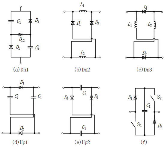
Figure 19.
Basic simple voltage multipliers. (a) Dn1. (b) Dn2. (c) Dn3. (d) Up1. (e) Up2. (f) [39].

Table 4.
Circuits and voltage gains for specific voltage multipliers.
It can be seen that a wide gain voltage range can be achieved using a simple structure and method, with this method being very efficient.
The above structure is composed of diodes and capacitors or diodes and inductors. The following will introduce two structures composed of three kinds of devices. The structure of Figure 20a, used in [40], replaces the diode of the Cuk circuit with the multiplier above, and the resulting efficiency is approximately 97% when the D is 0.75, making its gain double as:
M = 2D/(1 − D),
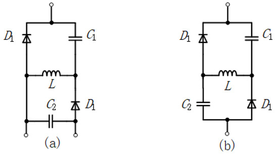
Figure 20.
Basic voltage multipliers. (a) [40]. (b) A simple voltage multiplier.
Similarly, the structure in Figure 20b replaces the diode in the Zeta circuit with a new topology. The voltage gain is same as above, but the input current is discontinuous. In addition, the active switch in the circuit can be replaced to realize a circuit voltage change [39], and the switch in the traditional buck–boost circuit can be replaced by the structure shown in Figure 19f to obtain a new topology. Both switches are turned on and off at the same time, and the resulting voltage gain is:
M = 2D/(1 − 2D),
3.3. Switched Inductor
Voltage lift is also a common technique in buck–boost converters. It involves charging the capacitor to a certain voltage and then increasing the voltage step by step to achieve the goal of changing the voltage. Generally speaking, it uses switched inductors in buck–boost circuits instead of inductors in the circuit to achieve voltage change and can be used in multi-level converters [41].
The first switched inductor can step-up voltage, the structure of which is shown in Figure 21a. It can replace the inductor in traditional buck–boost, Cuk, SEPIC, and Zeta converters to change the voltage gain in the circuit. Table 5 shows the voltage gain of the changed topology.
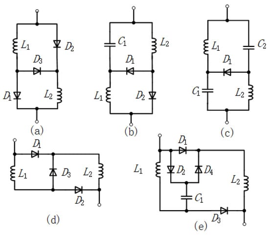
Figure 21.
Switched inductors. (a) [37]. (b) [42]. (c) [43]. (d,e) [44].

Table 5.
Circuits and voltage gain for UP3.
The first switched inductor can step-up voltage, the structure of which is shown in Figure 21a [37]. It can replace the inductor in traditional buck–boost, Cuk, SEPIC, and Zeta converters to change the voltage gain in the circuit. Table 5 shows the voltage gain of the changed topology. A switched inductor composed of diodes, capacitors, and inductors was proposed in [42,45], as shown in Figure 21b. The efficiency varies from 91% to 96% when the output voltage is 48 V. This is used in the traditional buck–boost circuit in this paper. Its input and output port are common ground, and its gain is square, which means it can boost and buck voltage. Its gain is:
M = D(2 − D)/(1 − D)2,
As shown in Figure 21c, the structure was applied to SEPIC circuit, and a high efficiency converter with twice the original voltage gain was obtained [45], with the efficiency being approximately 97% in the experiment. Two kinds of switched inductors were introduced in [44], as shown in Figure 21d,e, respectively. A new topology structure was proposed by using the switched inductor and voltage multiplier in the figure. The resulting efficiency gain was:
M = (2N − 1 + D)/(1 − D),
3.4. Different Ways of Connecting
One well-known way to change the voltage gain of a DC–DC converter is to change the way the circuit is connected. In this section, cascading, interleaving, and multi-level converters are described. In this structure, the voltage gain is transformed linearly or exponentially as a function of the topology used.
Cascading involves connecting the output port of one converter with the input port of the next converter. There are two ways to achieve this: one uses the same circuit topologies, which can be combined into a new circuit structure with its own characteristics through different connection modes in terms of topology; the other uses a hybrid cascade, where the circuits that are connected together are different.
By connecting two traditional buck–boost converters together, a cascaded structure can be obtained, as shown in Figure 22a. Since the output voltage of a buck–boost circuit is negative and the efficiency is approximately 90%, the final output voltage of the circuit is positive, and its voltage gain is as follows:
M = D2/(1 − D)2,
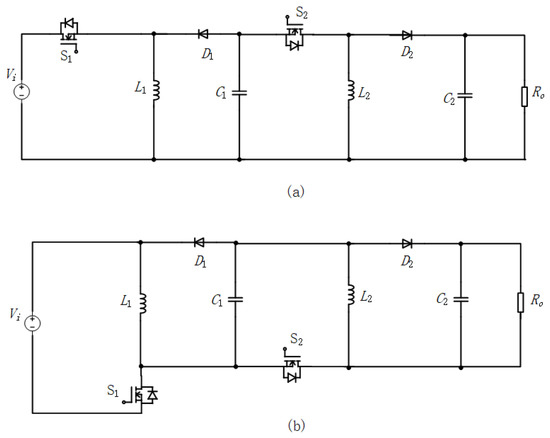
Figure 22.
Basic quadratic DC-DC converters. (a) Basic structure. (b) Improved structure.
According to the needs, two switches can operate at different operating frequencies and duty cycles. The new topology structure, as shown in Figure 22b, can be obtained by changing the position of the first-stage switch in this circuit. It is characterized by low voltage stress on the inductor and low current stress on the capacitor under continuous conduction mode (CCM). The efficiency is approximately 92% when the D is 0.5. A traditional quadratic buck–boost converter was introduced in [46], as shown in Figure 23a. It has only one switch, so it can only operate at a specific frequency and duty cycle, and its output is negative. Two cascaded buck–boost converters were introduced in [47,48], as shown in Figure 23b,c, respectively. In Figure 23b, the efficiency in step-up mode is higher than in step-down mode. The highest efficiency was approximately 92.05% in the experiment. Of course, multiple modules can also be cascaded, with this not being limited to two, but a large number of modules will increase the voltage and current stress of the device and reduce the efficiency of the circuit.
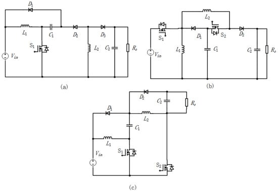
Figure 23.
Basic quadratic buck-boost DC-DC converters. (a) [46]. (b) [47]. (c) [48].
The so-called hybrid cascade involves connecting the input port of one circuit to the output port of another completely different circuit, with the resulting voltage gain being the product of the original voltage gain of the two circuits. A topology that is cascaded by a boost converter and a Cuk converter was introduced in [49], as shown in Figure 24. The highest efficiency was approximately 91% in the experiment. It has only one switch, and the input and output current are continuous. The output gain is:
M = D/(1 − D)2,
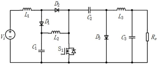
Figure 24.
A hybrid cascaded DC-DC converter.
Multiple different circuits can be connected in this way at the same time. For example, a single switch circuit is described in [50] which consists of a cascade of a boost, buck–boost, and buck converter.
Interleaving is also a technique that can change the voltage gain. The authors of [51] introduced a relatively classical and simple interleaved buck–boost converter, as shown in Figure 25a. The authors of [52] introduced a bidirectional cascaded buck–boost converter, as shown in Figure 25b, with the efficiency in boost mode being higher than in buck mode. The efficiency varies from 93.2% to 95.2%. The design has a relatively small number of components and does not use auxiliary circuits, so the current ripple and the loss is small. The circuit can realize the bidirectional flow of power through four switches and body diodes in continuous conduction mode (CCM). When the power is flowing forward, this is achieved by using the body diodes of S1 and S2 and S3 and S4. In a cycle, it can be divided into four working phases. In the first half cycle, in the first phase, S1 and D3 are on but S2 and D4 are off. In the second phase, D3 and D4 are on but S1 and S2 are off. In the other half cycle, in the first phase, S2 and D4 are on but S1 and D3 are off. In the second phase, D3 and D4 are on but S1 and S2 are switched off. When the power flows in reverse, the operation mode is the same as above, but the power flows through the S3 and S4 and S1 and S2 body diodes to achieve this. The converter has a wide range of output voltages and a positive output voltage. The authors of [53] describe a cascade interleaved circuit which consists of a two-phase interleaved buck converter, a two-phase interleaved boost converter, and two filter capacitors, as shown in Figure 25c. It can work in buck or boost mode. When operating in buck mode, it turns off S1 and S2 and controls the switch-on and switch-off of S3 and S4. When working in boost mode, it turns S3 and S4 on and controls S1 and S2 to switch on and off. The circuit is cascaded in such a way that the input current of all inductors is the same, resulting in improved circuit efficiency and reduced current ripple. The ripple percentage of the input current is approximately 9.26%. An interleaved bidirectional buck–boost converter was introduced in [54] which can achieve high dynamic response and high efficiency under the condition of double closed-loop current and voltage control.
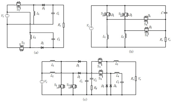
Figure 25.
Interleaved buck-boost DC-DC converters. (a) [51]. (b) [52]. (c) [53].
Multi-level connection is a technique that uses a modular structure to realize a gain level increment which is not the product of the gain of two circuits, as in a cascade. Multi-level connection can be used for both single-input DC source and multi-input DC source converters. As shown in Figure 26a, a module composed of inductors, diodes, and capacitors was introduced in [55]. Multi-level buck–boost converters are realized by using this module. The voltage gain depends on the number of modules. According to the literature, the efficiency of such converters is approximately 96%, their output voltage is negative, and their gain is:
M = nD/(1 − D),
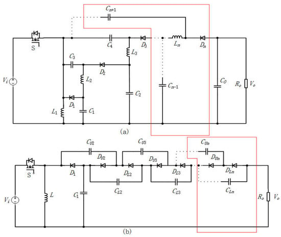
Figure 26.
Multi-level buck-boost converters with single DC source. (a) [55]. (b) [56].
A multi-level buck–boost converter with a voltage multiplier was introduced in [56]. The voltage multiplier is composed of diodes and capacitors, and it is composed of a multi-level structure added after the buck–boost converter, as shown in Figure 26b. In the three levels, the efficiency is close to 93%. Its output voltage is also negative. Its voltage gain is:
M = (N − 1 + D)/(1 − D),
Multi-input levels are composed of multiple input sources, which can increase the output voltage. This has the advantages of high reliability, low costs, and good security. The principle is also very simple. Multiple DC sources generate voltage on the output capacitor, which add together to achieve the purpose of changing the output voltage. A novel SEPIC-based multi-input DC/DC converter that can be used in photovoltaic systems and fuel cells was described in [57], as shown in Figure 27a. At the same time, there are multiple input ports so that the input of various renewable energy systems can be realized. As indicated in [58], because a distributed generator (DG) applying a several single-input DC–DC converter may lead to complex procedures and controls, high losses, large volumes, and less efficiency, multi-input DC–DC converters can be used. A new multi-input topology that can be used for RES was proposed in [59], as shown in Figure 27b. Here is how the two input sources work in buck–boost mode. In the first phase, the battery can be charged by V1 through S2 in charging mode or discharged to the inductor through S1 in discharging mode. In the second phase, V1 charges the inductor through D2, S3, and T1. In the third phase, V1 and V2 simultaneously charge the inductor through T1, T2, and S3. Finally, the inductor discharges the output capacitor through D1, D2, and S4. The circuit uses fewer switches to realize the bidirectional flow of energy, which increases the efficiency and reduces the complexity in terms of control. It can work in buck, boost, or buck–boost mode, has more comprehensive functions, and only needs one inductor. The excess energy can be absorbed by the battery and then released, thus improving the utilization rate in terms of energy.
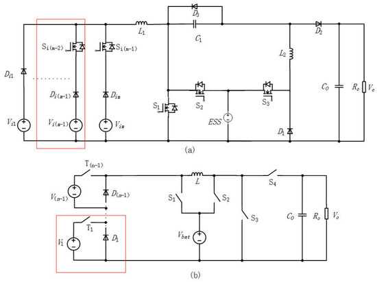
Figure 27.
Multi-input step-up and step-down DC-DC converters. (a) [57]. (b) [59].
A summary of the techniques used in step-up and step-down DC–DC converters is provided in Table 6.

Table 6.
Summary of techniques used in step-up and step-down DC-DC converters.
4. Application
In recent years, with the rapid development of power electronics technology, the step-up and step-down DC–DC converter has been widely used in various fields of industrial production and family life, no matter if it is unidirectional or bidirectional, single-input or multi-input, because it is highly efficient, simple, and can provide step-up and step-down voltage. They have been used in, for example, renewable energy systems including photovoltaic systems, fuel cells, wind energy, etc., LED lighting systems, electric vehicles, DC microgrids, HVDC systems, energy storage systems, integrated circuits with power supplies of 3.3 V and 1.5 V, aviation systems, telecommunications, solid state lighting systems, portable devices such as laptops and mobile phones, power factor correction, and so on. As this demonstrates, the step-up and step-down DC–DC converter is very common. However, its location, the required voltage level, the power level, and control mode are different according to its application. Over the years, various researchers have designed, developed, and improved its topology and control methods in order to achieve more complete, suitable, and advanced functions, so that it can be used in specific areas more efficiently and cleanly in a more lightweight, simple, economical, and stable fashion [60,61,62,63,64,65,66,67,68].
First of all, due to the depletion of fossil fuels in recent years, the increase in global carbon emissions, global warming, and environmental pollution as well as other factors, the renewable energy system has become the focus of attention and been put into use by countries all over the world. Renewable energy systems include photovoltaic and fuel cells, which are already widely used for industrial and household electricity. However, different power sources produce different voltage and current characteristics. For example, when they are integrated in the power grid, their voltage needs to be increased to control the energy flow to the power grid, while when they are used as the energy of certain household appliances, their voltage needs to be reduced to avoid the damage caused by overvoltage. At the same time, the variability and intermittency of renewable energy power supply is also an obvious shortcoming, with it being affected by weather, month, day and night, and other factors, resulting in a large range of power and voltage changes. Bidirectional buck–boost converters can be used in renewable energy systems. For example, in PV distribution generation, when the DC bus requires less energy, an excess output power is stored in the battery. During peak hours, when more energy is needed, the energy previously stored in the battery is transmitted back to the DC bus (usually 380 V) by a bidirectional DC converter. The above requirements indicate that a wide voltage range in terms of the step-up and step-down DC–DC converter is needed to solve this problem so as to make better use of renewable energy [16,60].
In lighting systems, LEDs have been widely used in recent years because of their long life, high efficiency, modularity, strong stability, and other advantages. Additionally, LEDs are solid state components, so they do not have a fragile envelop [61]. They are relatively robust and not filled with toxic gases. Because they are not associated with the possibility of explosion, breakage, or contamination, they are considered to be environmentally friendly and safe. LEDs can be used for white lighting as well as other colors of light lighting, so as to be more beautiful and convenient. Previously, their efficiency ranged from a typical 17 lm/W for blue light to 40 lm/W for red light. LEDs that emit white light are in the midrange of 35 lm/W. New single power LEDs typically have a power of 1 W, 3 W, or 5 W. They are also more energy efficient than incandescent bulbs, with recent industry studies showing that LED energy efficiency has exceeded 100 lm/W. As the light color changes and the brightness need voltage regulation, a converter handles the voltage regulation.
With the increasing use of low voltage portable devices and the popularity of wireless applications as well as the growing demand for features embedded in these devices, longer life batteries and lower input voltages have become the focus of research, with this requiring efficient power management techniques. Due to the variability of battery voltages (for example, the Li-ion battery voltage conversion range is 2.7–4.2 V), the system needs to use a voltage converter to output voltage that can be higher than the battery voltage or lower than the battery voltage to achieve a longer service life [62]. The single NiMH battery could be fully charged to 1.8 V, but its voltage dropped to 0.9 V before it was fully discharged. Therefore, such systems require step-up and step-down voltage.
DC–DC converters are widely used in telecommunication systems because of their advantages in terms of large power density, good reliability, and dynamic characteristics. Telecommunication systems usually have a wide range of voltage variations. For example, the nominal voltage of 48 V varies from 36 V to 75 V, so it is difficult to design a DC–DC modular source with high efficiency within the line range. In addition, in a telecommunication system with a DC voltage of 400 V, in order to ensure the UPS, it is usually necessary to use a backup battery with a bidirectional DC–DC converter to meet the demand [63].
In the field of electric vehicles, due to the exhaustion of fossil fuels and electric vehicles with strong energy storage capacity, better efficiency, and cleaner, the electric vehicle industry has also begun to flourish. In an EV, the energy sources mainly include batteries and solar and fuel cells and so on. Lithium-ion batteries are popular thanks to their high power density and efficiency as well as their capabilities and reliability in terms of charging. Both isolated and non-isolated DC–DC converters can be used, with the latter being more extensive. The modeling and charging of electric vehicle batteries are very popular topics in the research surrounding electric vehicle batteries [64,65]. It is worth noting that a switch mode power supply is vital for electric vehicle innovation. An efficient, simple DC–DC converter with a wide voltage conversion range is very important for battery charging and discharging. In electric vehicle systems, a relatively low voltage charges the on-board battery, but it must provide a high output voltage to drive the motors. Most electric cars use bidirectional buck–boost converters for the battery charging process. In general, input and output voltage ranges are 20–50 V and 150–300 V, respectively, for most DC–DC converters in an EV. Therefore, the amount of components is great, and the efficiency is approximately 94–98%. Traditional buck–boost converters are simple and effective, but they do not provide high voltage gain. Therefore, a topology with a wider gain and higher efficiency is needed.
The boost topology is very important in power factor correction applications because it can offer an output DC voltage which is close to but greater than the peak AC input voltage [66]. The efficiency in [66] was over 93%. For example, in general input applications, when the RMS of the input line voltage varies between 90 and 305 V, the output voltage is, correspondingly, approximately 450 V. When the RMS is 90 V, the RMS of the input current in the circuit is the maximum and the maximum voltage conversion ratio is required, which leads to maximum switch conduction losses in the circuit. In such cases, the size of the universal input of inductors should be designed to be larger than that of the input voltage in the narrow gain range. Moreover, because the output energy storage filter capacitor is large and the input features an inrush current, extra components need to be added to deal with this problem. In general input power factor correction applications, the ability of the converter to provide step-up and step-down voltage is important and welcome because the output DC voltage can be set to any value. Therefore, specific improved buck–boost converters are required. In Table 7, the features of DC–DC converters in different application are presented.

Table 7.
Summary of applications in step-up and step-down DC–DC converters.
5. Conclusions
In the first section, this paper briefly introduced the origin, characteristics, and operational principles of converters. They were then classified according to their different characteristics in Section 2. In the third section, techniques for changing voltage gain were provided. In the fourth section, the main applications of converters were described in detail. It is evident that current non-isolated step-up and step-down DC–DC converters are booming and that users will have higher demands in terms of their power density, volume, weight, voltage gain range, efficiency, stability, cost, and so on in the future. Therefore, in order to make breakthroughs in these area, several aspects will be vital. The first is a further breakthrough in terms of control modes and strategies. A good control strategy can result in the circuit having a better running process and contribute to an enhancement in performance. Secondly, researchers may study and explore more high-performance topologies. Although topology structures may not have comprehensive functions, they should achieve functionality in one or several contexts. This way, a converter can be dedicated to a certain field, which may become a trend in terms of the development of converters in the future. Finally, progress could be made in device materials, as the generation and development of power electronics technology and the renewal of power electronic devices are directly related. So-called DC–DC converters are composed of power electronic devices, so the quality of the devices themselves directly affect the operation and performance of the circuits, with the devices themselves therefore being important in the future development of converters. As for the applications of converters, due to global fossil fuel and climate problems, renewable energy systems will remain a hot spot in the future. And because of the popularization of electronic products in every area of people’s lives, electronic products will be further applied. There are also many areas that require investment new equipment in order to grow. Therefore, researchers will make more effort to promote the progress of non-isolated step-up and step-down DC–DC converters.
Author Contributions
F.Y. conceived, validated, and wrote the manuscript. F.W. participated in the research plan development and revised the manuscript. All authors have read and agreed to the published version of the manuscript.
Funding
This research received no external funding.
Institutional Review Board Statement
Not applicable.
Informed Consent Statement
Not applicable.
Data Availability Statement
Not applicable.
Conflicts of Interest
The authors declare that there are no conflicts of interest regarding the publication of this paper.
References
- Zhang, G.; Li, Z.; Zhang, B.; Halang, A.W. Power Electronic Converters: Past, Present and Future. Renew. Sustain. Energy Rev. 2018, 81, 2028–2044. [Google Scholar] [CrossRef]
- Bose, B.K. The past, present, and future of power electronics. Ind. Electron. Mag. IEEE 2009, 3, 7–11. [Google Scholar] [CrossRef]
- Van Wyk, J.D. Power Electronics Technology At the Dawn of a New Century-Past Achievements and Future Expectations. In Proceedings of the 2000 3rd International Power Electronics and Motion Control Conference, Beijing, China, 15–18 August 2000; pp. 9–20. [Google Scholar]
- Ding, S.; Wang, F. A New Negative Output Buck–Boost Converter with Wide Conversion Ratio. IEEE Trans. Ind. Electron. 2017, 64, 9322–9333. [Google Scholar]
- Banaei, M.R.; Bonab, H.A.F. A Novel Structure for Single-Switch Nonisolated Transformerless Buck–Boost DC–DC Converter. IEEE Trans. Ind. Electron. 2017, 64, 198–205. [Google Scholar] [CrossRef]
- Sarikhani, A.; Allahverdinejad, B.; Torkaman, H. A non-isolated buck-boost DC-DC converter with single switch. In Proceedings of the 2018 9th Annual Power Electronics, Drives Systems and Technologies Conference, Tehran, Iran, 13–15 February 2018; pp. 369–373. [Google Scholar]
- Forouzesh, M.; Siwakoti, Y.P.; Gorji, S.A.; Blaabjerg, F.; Lehman, B. Step-Up DC–DC Converters: A Comprehensive Review of Voltage-Boosting Techniques, Topologies, and Applications. IEEE Trans. Power Electron. 2017, 32, 9143–9178. [Google Scholar] [CrossRef]
- Mohapatra, T.K.; Dey, A.K.; Mohapatra, K.K. A Novel Non-isolated Positive Output TA Converter. In Proceedings of the 2019 IEEE International Conference on Sustainable Energy Technologies and Systems, Bhubaneswar, India, 26 February–1 March 2019; pp. 7–12. [Google Scholar]
- Luo, F. Six self-lift DC-DC converters, voltage lift technique. IEEE Trans. Ind. Electron. 2001, 48, 1268–1272. [Google Scholar]
- Lu, J.; Wu, H.; Shi, W. A non-isolated bidirectional Buck-Boost converter with minimized reverse-recovery losses. In Proceedings of the IECON 2011—37th Annual Conference of the IEEE Industrial Electronics Society, Melbourne, VIC, Australia, 7–10 November 2011; pp. 1085–1090. [Google Scholar]
- Saeed, L.; Khan, M.Y.A.; Arif, M.; Majid, A.; Saleem, J. A multiple-input multiple-output non-inverting non-isolated bidirectional buck/boost converter for storage application. In Proceedings of the 2018 IEEE International Conference on Computing, Mathematics and Engineering Technologies, Sukkur, Pakistan, 3–4 March 2018; pp. 1–6. [Google Scholar]
- Fardoun, A.A.; Ismail, E.H.; Sabzali, A.J.; Al-Saffar, M.A. Bidirectional converter with low input/output current ripple for renewable energy applications. In Proceedings of the 2011 IEEE Energy Conversion Congress and Exposition, Phoenix, AZ, USA, 17–22 September 2011; pp. 3322–3329. [Google Scholar]
- Xiong, S.; Tan, S.C. Cascaded High-Voltage-Gain Bidirectional Switched-Capacitor DC–DC Converters for Distributed Energy Resources Applications. IEEE Trans. Power Electron. 2017, 2, 220–1231. [Google Scholar] [CrossRef]
- Lin, C.C.; Yang, L.S.; Wu, G. Study of a non- isolated bidirectional DC-DC converter. IET Power Electron. 2013, 6, 30–37. [Google Scholar] [CrossRef]
- Ardi, H.; Ajami, A.; Kardan, F.; Avilagh, S.N. Analysis and Implementation of a Nonisolated Bidirectional DC–DC Converter With High Voltage Gain. IEEE Trans. Ind. Electron. 2016, 63, 4878–4888. [Google Scholar]
- Chen, M.M.; Cheng, K.W.E. A new bidirectional DC-DC converter with a high step-up/down conversion ratio for renewable energy applications. In Proceedings of the 2016 International Symposium on Electrical Engineering (ISEE), Hong Kong, China, 14 December 2016; pp. 1–6. [Google Scholar]
- Tymerski, R.; Vorperian, V. Generation and classification of PWM DC-to-DC converters. IEEE Trans. Aerosp. Electron. Syst. 1988, 24, 743–754. [Google Scholar] [CrossRef]
- Capel, A.; Marpinard, J.C.; Jalade, J.; Valentin, M. Current Fed and Voltage Fed Switching DC/DC Converters—Steady State and Dynamic Models their Applications in Space Technology. In Proceedings of the Fifth International Telecommunications Energy Conference, Tokyo, Japan, 18–21 October 1983; pp. 421–430. [Google Scholar]
- Nousiainen, L.; Suntio, T. Dynamic characteristics of current-fed semi-quadratic buck-boost converter in photovoltaic applications. In Proceedings of the 2011 IEEE Energy Conversion Congress and Exposition, Phoenix, AZ, USA, 17–22 September 2011; pp. 1031–1038. [Google Scholar]
- Rathore, A.K.; Patil, D.R.; Srinivasan, D. Non-isolated Bidirectional Soft-Switching Current-Fed LCL Resonant DC/DC Converter to Interface Energy Storage in DC Microgrid. IEEE Trans. Ind. Appl. 2016, 52, 1711–1722. [Google Scholar] [CrossRef]
- Vashisth, N.; Gupta, R. A study of different hard-switched and soft-switched variants of buck-boost converter. In Proceedings of the 2016 IEEE 7th Power India International Conference, Bikaner, India, 25–27 November 2016; pp. 1–6. [Google Scholar]
- Behera, S.; Kumar, B.; Behera, R.; Panigrahi, B.P.; Behera, R.K.; Bagarty, D.P. Regulated Soft-Switching Power Supply Using Buck-Boost Converter. In Proceedings of the 2020 International Conference on Computational Intelligence for Smart Power System and Sustainable Energy, Keonjhar, India, 29–31 July 2020; pp. 1–7. [Google Scholar]
- Cheng, X.F.; Liu, C.; Wang, D.; Zhang, Y. State-of-the-Art Review on Soft-Switching Technologies for Non-Isolated DC-DC Converters. IEEE Access 2021, 9, 119235–119249. [Google Scholar] [CrossRef]
- Kiran, B.R.; Ezhilarasi, G.A. Design and analysis of soft-switched Buck-Boost Converter for PV applications. In Proceedings of the 2015 Annual IEEE India Conference, New Delhi, India, 17–20 December 2015; pp. 1–5. [Google Scholar]
- Wu, T.F.; Liang, S.A. A systematic approach to developing single-stage soft switching PWM converters. IEEE Trans. Power Electron. 2001, 16, 581–593. [Google Scholar]
- Wu, T.F.; Liang, S.A.; Lee, C.H. A unified approach to developing soft switching PWM converters. In Proceedings of the 2000 IEEE 31st Annual Power Electronics Specialists Conference, Galway, Ireland, 23 June 2000; pp. 193–198. [Google Scholar]
- Kim, J.G.; Park, S.W.; Kim, Y.H.; Jung, Y.C.; Won, C.Y. High-efficiency bidirectional soft switching DC-DC converter. In Proceedings of the 2010 International Power Electronics Conference, Sapporo, Japan, 21–24 June 2010; pp. 2905–2911. [Google Scholar]
- Hua, G.; Yang, E.X.; Jiang, Y.; Lee, F.C. Novel zero-current-transition PWM converters. In Proceedings of the IEEE Power Electronics Specialist Conference, Seattle, WA, USA, 20–24 June 1993; pp. 538–544. [Google Scholar]
- Hua, G.; Leu, C.; Jiang, Y.; Lee, F.C.Y. Novel zero-voltage-transition PWM converters. IEEE Trans. Power Electron. 1994, 9, 213–219. [Google Scholar]
- Kwak, D.K.; Lee, S.H.; Jung, D.Y. A new buck-boost DC/DC converter of high efficiency by soft switching technique. In Proceedings of the 2009 IEEE 6th International Power Electronics and Motion Control Conference, Wuhan, China, 17–20 May 2009; pp. 1295–1299. [Google Scholar]
- Bhajana, V.V.S.K.; Drabek, P. A novel ZCS bidirectional buck-boost DC-DC converters for energy storage applications. In Proceedings of the 2015 IEEE International Conference on Industrial Technology, Seville, Spain, 17–19 March 2015; pp. 872–877. [Google Scholar]
- Seeman, M.D.; Sanders, S.R. Analysis and Optimization of Switched-Capacitor DC–DC Converters. IEEE Trans. Power Electron. 2008, 23, 841–851. [Google Scholar] [CrossRef]
- Eguchi, K.; Hirata, S.; Shimoji, M.; Zhu, H. Design of a Step-Up/Step-Down k (=2,3,…)-Fibonacci DC-DC Converter Designed by Switched-Capacitor Techniques. In Proceedings of the 2012 Fifth International Conference on Intelligent Networks and Intelligent Systems, Tianjin, China, 1–3 November 2012; pp. 170–173. [Google Scholar]
- Abbasi, M.; Babaei, E.; Tousi, B. New family of non-isolated step-up/down and step-up switched-capacitor-based DC–DC converters. IET Power Electron. 2019, 12, 1706–1720. [Google Scholar] [CrossRef]
- Abbasi, M.; Abbasi, E.; Tousi, B.; Gharehpetian, G.B. New family of expandable step-up/-down DC-DC converters with increased voltage gain and decreased voltage stress on capacitors. Int. Trans. Electr. Energy Syst. 2020, 30, 1–17. [Google Scholar] [CrossRef]
- Abbasi, M.; Abbasi, E.; Li, L.; Tousi, B. Design and Analysis of a High-Gain Step-Up/Down Modular DC–DC Converter with Continuous Input Current and Decreased Voltage Stress on Power Switches and Switched-Capacitors. Sustainability 2021, 13, 5243. [Google Scholar] [CrossRef]
- Axelrod, B.; Berkovich, Y.; Ioinovici, A. Switched-Capacitor/Switched-Inductor Structures for Getting Transformerless Hybrid DC–DC PWM Converters. IEEE Trans. Circuits Syst. I Regul. Pap. 2008, 55, 687–696. [Google Scholar] [CrossRef]
- Axelrod, B.; Berkovich, Y.; Ioinovici, A. Switched-capacitor (SC)/switched inductor (SL) structures for getting hybrid step-down Cuk/Sepic/Zeta converters. In Proceedings of the 2006 IEEE International Symposium on Circuits and Systems, Kos, Greece, 21–24 May 2006; p. 4. [Google Scholar]
- Veerachary, M. Switching Capacitor Assisted Buck-Boost Converter. In Proceedings of the 2021 International Conference on Sustainable Energy and Future Electric Transportation (SEFET), Hyderabad, India, 21–23 January 2021; pp. 1–6. [Google Scholar]
- Banaei, M.R.; Ardi, H.; Farakhor, A. Analysis and implementation of a new single switch buck-boost converter. IET Power Electron. 2014, 7, 1906–1914. [Google Scholar] [CrossRef]
- Alateeq, A.; Almalaq, Y.; Matin, M. A switched-inductor model for a non-isolated multilevel boost converter. In Proceedings of the 2017 North American Power Symposium, Morgantown, WV, USA, 17–19 September 2017; pp. 1–5. [Google Scholar]
- Gorji, S.A.; Mostaan, A.; My, H.T.; Ektesabi, M. Non-isolated buck–boost DC–DC converter with quadratic voltage gain ratio. IET Power Electron. 2019, 12, 1425–1433. [Google Scholar] [CrossRef]
- Banaei, M.R.; Bonab, H.A.F. High efficiency transformerless buck boost DC/DC converter. Int. J. Circuit Theory Appl. 2017, 45, 1129–1150. [Google Scholar] [CrossRef]
- Bhaskar, M.S.; SreeramulaReddy, N.; Kumar, R.K.P.; Gupta, Y.B.S.S. A novel high step-up DC-DC multilevel buck-boost converter using voltage-lift switched-inductor cell. In Proceedings of the IEEE International Conference on Computer Communication and Systems, Chennai, India, 20–21 February 2014; pp. 271–275. [Google Scholar]
- Mostaan, A.; Gorji, S.A.; Soltani, M.N.; Ektesabi, M. A novel single switch transformerless quadratic DC/DC buck-boost converter. In Proceedings of the 2017 19th European Conference on Power Electronics and Applications, Warsaw, Poland, 11–14 September 2017; pp. 1–6. [Google Scholar]
- Maksimovic, D.; Cuk, S. General properties. synthesis of PWM DC-to-DC converters. In Proceedings of the 20th Annual IEEE Power Electronics Specialists Conference, Milwaukee, Wisconsin, 26–29 June 1989; pp. 515–525. [Google Scholar]
- Miao, S.; Wang, F.; Ma, X. A New Transformerless Buck–Boost Converter with Positive Output Voltage. IEEE Trans. Ind. Electron. 2016, 63, 2965–2975. [Google Scholar] [CrossRef]
- Mostaan, A.; Gorji, S.A.; Soltani, M.; Ektesabi, M. A novel quadratic buck-boost DC-DC converter without floating gate-driver. In Proceedings of the 2016 IEEE 2nd Annual Southern Power Electronics Conference (SPEC), Auckland, New Zealand, 5–8 December 2016; pp. 1–5. [Google Scholar]
- De Britto, J.R.; de Freitas, L.C.; Farias, V.J.; Coelho, E.A.A.; Vieira, J.B. A Non-Insulated Step-Up/Down DC-DC Converter with Wide Range Conversion. In Proceedings of the 2009 Twenty-Fourth Annual IEEE Applied Power Electronics Conference and Exposition, Houston, TX, USA, 15–19 February 2009; pp. 1374–1377. [Google Scholar]
- Zhang, N.; Zhang, G.; See, K.W.; Zhang, B. A Single-Switch Quadratic Buck–Boost Converter With Continuous Input Port Current and Continuous Output Port Current. IEEE Trans. Power Electron. 2018, 33, 4157–4166. [Google Scholar] [CrossRef]
- Ostos, J.C.; Lu, D.D.C. Modeling and analysis of CCM non-isolated high step-up interleaved buck-boost DC/DC converters. In Proceedings of the 2012 IEEE International Conference on Power and Energy (PECon), Kota Kinabalu, Malaysia, 2–5 December 2012; pp. 28–31. [Google Scholar]
- Yaser, B.; Mehran, S.; Babaei, E.; Sun, K. A New Continuous Input Current Nonisolated Bidirectional Interleaved Buck-Boost DC-DC Converter. Int. Trans. Electr. Energy Syst. 2022, 2022, 19. [Google Scholar]
- Gupta, R.; Gautam, S.; Kumar, M. Characterization and Design of Interleaved Buck-Boost Converter. In Proceedings of the 2022 IEEE IAS Global Conference on Emerging Technologies, Arad, Romania, 20–22 May 2022; pp. 593–598. [Google Scholar]
- Liu, F.; Zhao, Y.; Wu, Z.; Wang, W.; Wang, H.; Li, H. Interleaved Bidirectional Buck-Boost DC-DC Converter Based on Multi-mode Control. In Proceedings of the 2022 6th International Conference on Green Energy and Applications, online, 4–6 March 2022; pp. 182–186. [Google Scholar]
- Maalandish, M.; Hosseini, S.H.; Jalilzadeh, T.; Pourjafar, S. A Buck-Boost DC/DC Converter with High Efficiency Suitable for Renewable Energies. Int. J. Emerg. Electr. Power Syst. 2018, 19, 1–17. [Google Scholar] [CrossRef]
- Bhaskar, M.S.; Al-ammari, R.; Meraj, M.; Iqbal, A.; Padmanaban, S. Modified multilevel buck–boost converter with equal voltage across each capacitor: Analysis and experimental investigations. IET Power Electron. 2019, 12, 3318–3330. [Google Scholar] [CrossRef]
- Haghighian, S.K.; Tohid, S.; Feyzi, M.R.; Sabahi, M. Design and analysis of a novel SEPIC-based multi-input DC/DC converter. IET Power Electron. 2017, 10, 1393–1402. [Google Scholar] [CrossRef]
- Mounika, A.; Shankar, S.; Ramprabhakar, J. A Hybrid Energy Source Integration in a DC Microgrid using Multi- Input Buck-Boost Converter. In Proceedings of the 2018 4th International Conference for Convergence in Technology, Mangalore, India, 27–28 October 2018; pp. 1–6. [Google Scholar]
- Varesi, K.; Hosseini, S.H.; Sabahi, M.; Babaei, E. Performance analysis and calculation of critical inductance and output voltage ripple of a simple non-isolated multi-input bidirectional DC-DC converter. Int. J. Circuit Theory Appl. 2017, 46, 543–564. [Google Scholar] [CrossRef]
- Hua, C.; Tu, C. Design and implementation of power converters for wind generator. In Proceedings of the 2009 4th IEEE Conference on Industrial Electronics and Applications, Xi’an, China, 25–27 May 2009; 2009; pp. 3372–3377. [Google Scholar]
- De Britto, J.R.; Demian, A.E.; de Freitas, L.C.; Farias, V.J.; Coelho, E.A.A.; Vieira, J.B. A proposal of Led Lamp Driver for universal input using Cuk converter. In Proceedings of the 2008 IEEE Power Electronics Specialists Conference, Rhodes, Greece, 15–19 June 2008; pp. 2640–2644. [Google Scholar]
- Sahu, B.; Rincon-Mora, G.A. A low voltage, dynamic, noninverting, synchronous buck-boost converter for portable applications. IEEE Trans. Power Electron. 2004, 19, 443–452. [Google Scholar] [CrossRef]
- Ren, X.; Tang, Z.; Ruan, X.; Wei, J.; Hua, G. Four Switch Buck-Boost Converter for Telecom DC-DC power supply applications. In Proceedings of the 2008 Twenty-Third Annual IEEE Applied Power Electronics Conference and Exposition, Houston, TX, USA, 24–28 February 2008; pp. 1527–1530. [Google Scholar]
- Ortuzar, M.; Moreno, J.; Dixon, J. Ultracapacitor-Based Auxiliary Energy System for an Electric Vehicle: Implementation and Evaluation. IEEE Trans. Ind. Electron. 2007, 54, 2147–2156. [Google Scholar] [CrossRef]
- Samosir, A.S.; Yatim, A.H.M. Implementation of Dynamic Evolution Control of Bidirectional DC–DC Converter for Interfacing Ultracapacitor Energy Storage to Fuel-Cell System. IEEE Trans. Ind. Electron. 2010, 57, 3468–3473. [Google Scholar] [CrossRef]
- Chen, J.; Maksimovic, D.; Erickson, R. A new low-stress buck-boost converter for universal-input PPC applications. In Proceedings of the APEC 2001 Sixteenth Annual IEEE Applied Power Electronics Conference and Exposition, Anaheim, CA, USA, 4–8 March 2001; pp. 343–349. [Google Scholar]
- Rajaei, A.; Shahparasti, M.; Nabinejad, A.; Savaghebi, M. A high step-up partial power processing DC/DC T-source converter for ups application. Sustainability 2020, 12, 1–19. [Google Scholar] [CrossRef]
- Ferraz, P.; Kowal, J. A comparative study on the influence of DC/DC converter induced high frequency current ripple on lithium-ion batteries. Sustainability 2019, 11, 6050. [Google Scholar] [CrossRef]
Disclaimer/Publisher’s Note: The statements, opinions and data contained in all publications are solely those of the individual author(s) and contributor(s) and not of MDPI and/or the editor(s). MDPI and/or the editor(s) disclaim responsibility for any injury to people or property resulting from any ideas, methods, instructions or products referred to in the content. |
© 2023 by the authors. Licensee MDPI, Basel, Switzerland. This article is an open access article distributed under the terms and conditions of the Creative Commons Attribution (CC BY) license (https://creativecommons.org/licenses/by/4.0/).