Author Contributions
Conceptualization, K.R. and R.B.; methodology, R.B.; software, K.R. and K.G.; validation, R.B.; formal analysis, R.B. and K.R.; investigation, R.B., K.G., and K.R.; resources, K.G.; data curation, R.B. and K.R.; writing—original draft preparation, K.R.; writing—review and editing, R.B. and K.G.; visualization, K.R.; supervision, R.B.; project administration, R.B.; funding acquisition, R.B. and K.G. All authors have read and agreed to the published version of the manuscript.
Figure 1.
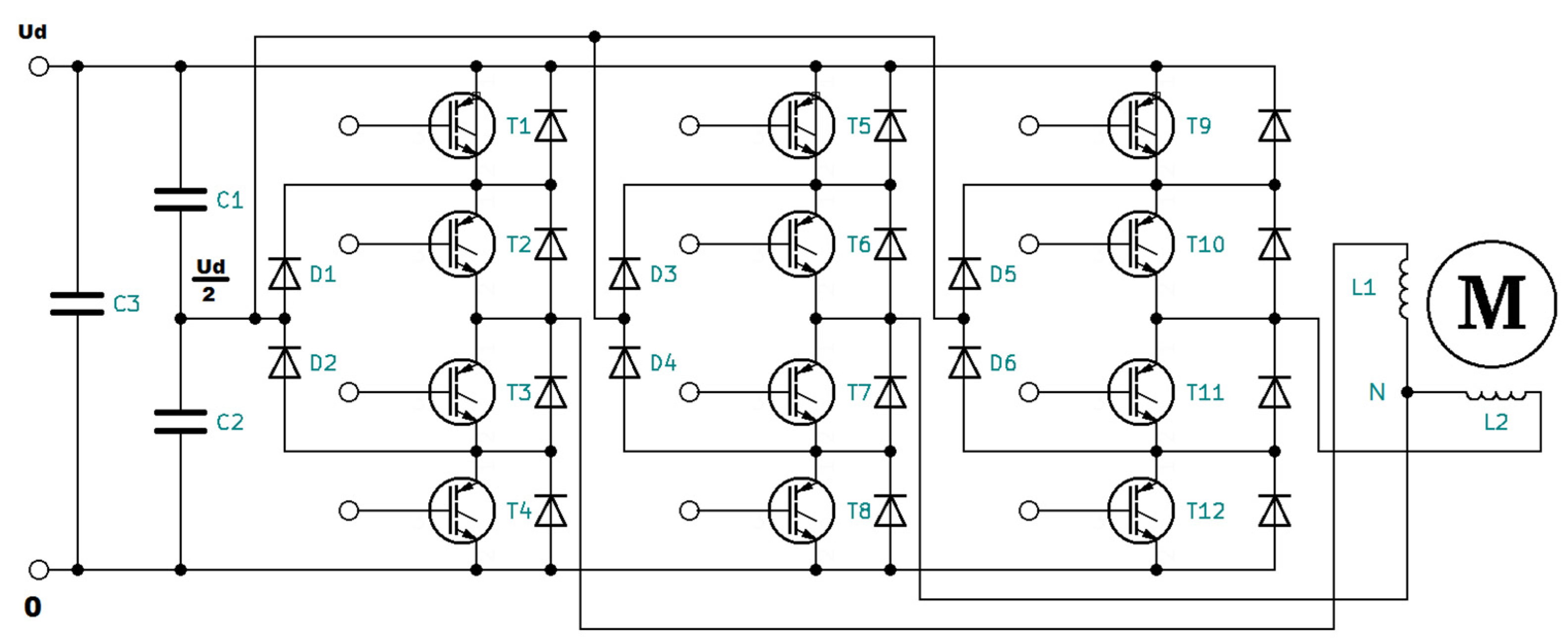
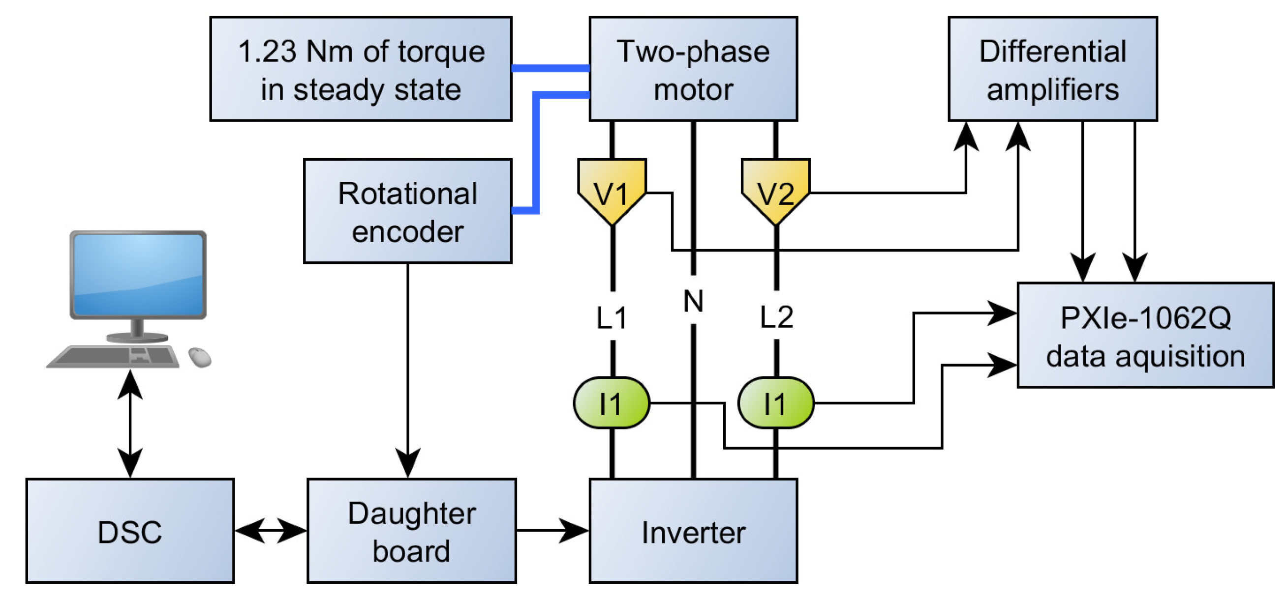
Three-leg three-level NPC inverter used to power a two-phase induction motor. T1–T12 are the IGBT transistors, D1–D6 are the neutral point clamping diodes, C1–C3 are the filtering capacitors, M is the two-phase squirrel cage induction motor, and L1–L2 are its windings.
Figure 1.
Three-leg three-level NPC inverter used to power a two-phase induction motor. T1–T12 are the IGBT transistors, D1–D6 are the neutral point clamping diodes, C1–C3 are the filtering capacitors, M is the two-phase squirrel cage induction motor, and L1–L2 are its windings.
Figure 2.
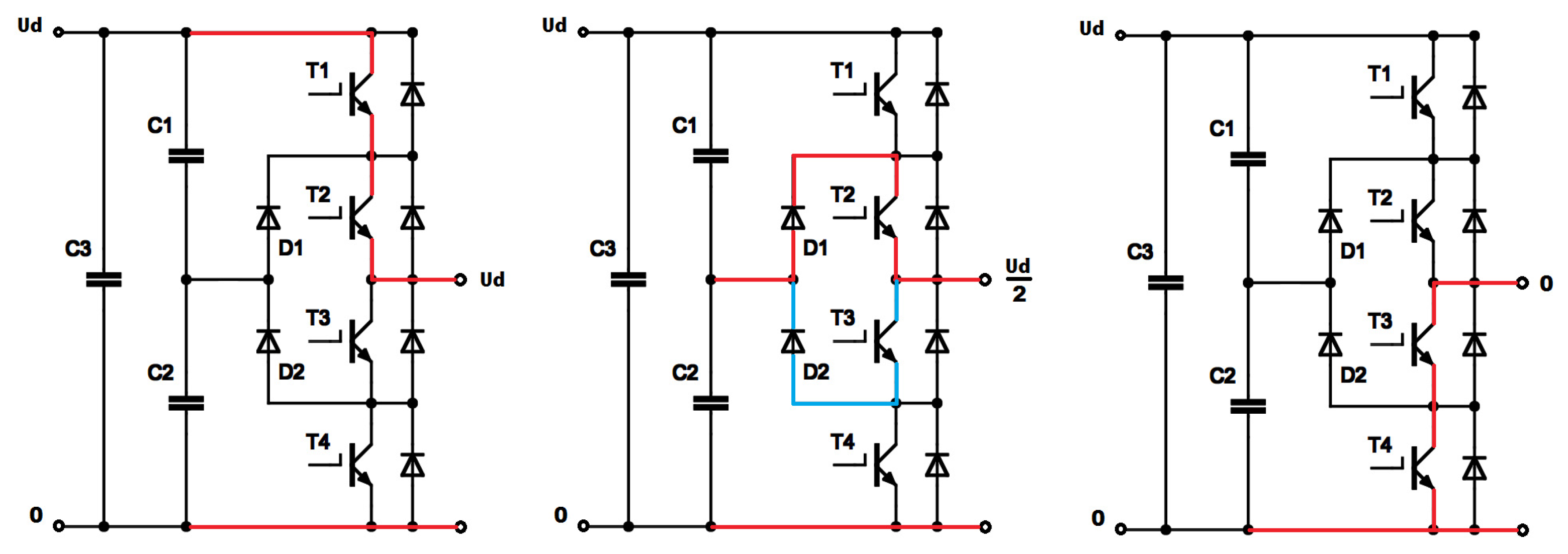
Output voltages of the 3L-NPC inverter: left—Ud, center—Ud/2, right—0, red line—current flow between capacitor and output terminals, blue line—alternative flow of current for Ud/2.
Figure 2.
Output voltages of the 3L-NPC inverter: left—Ud, center—Ud/2, right—0, red line—current flow between capacitor and output terminals, blue line—alternative flow of current for Ud/2.
Figure 3.
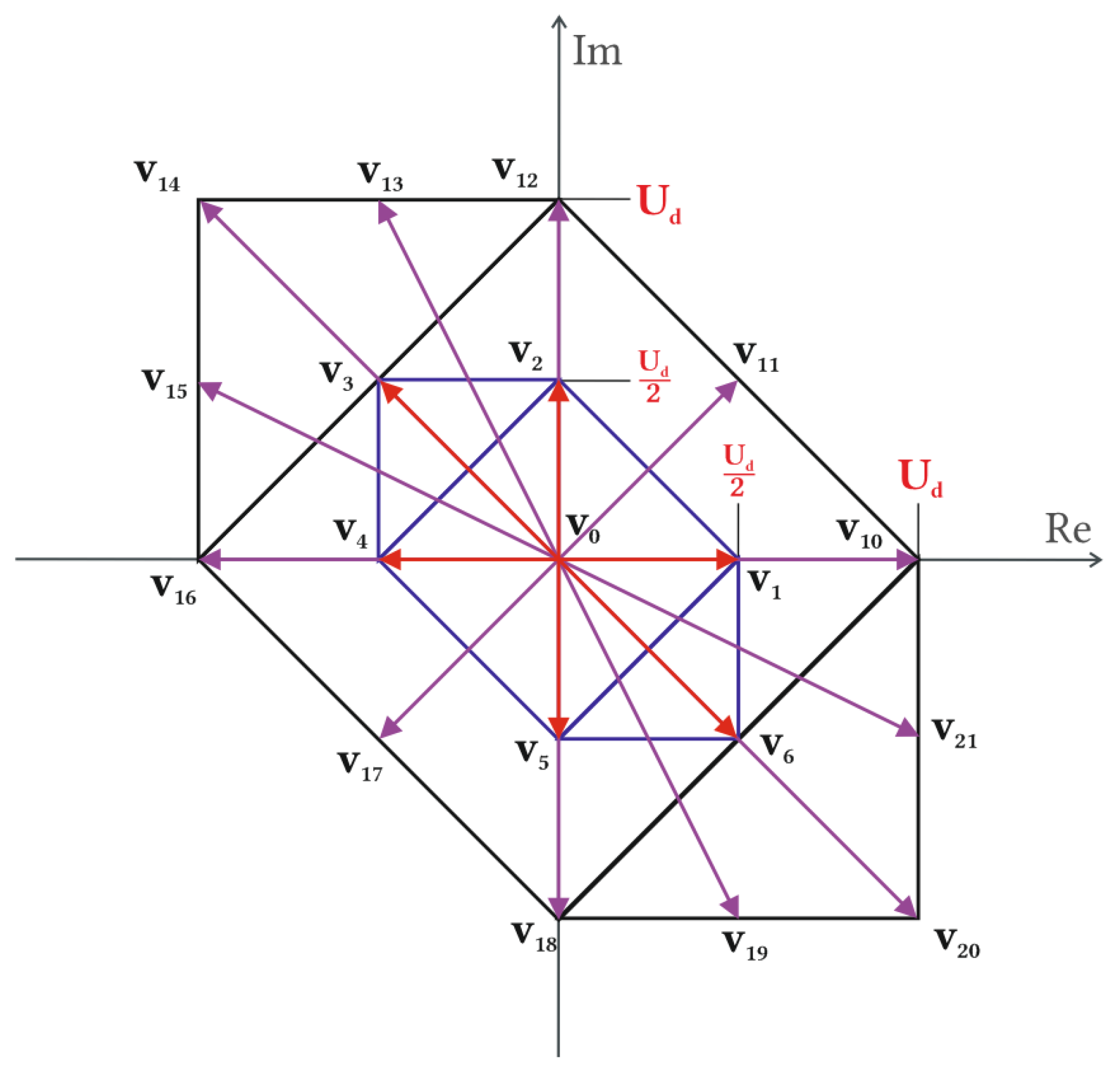
Nineteen output phase-to-phase voltage vectors of the two-phase 3L-NPC inverter represented in an α–β complex space forming a hexagon.
Figure 3.
Nineteen output phase-to-phase voltage vectors of the two-phase 3L-NPC inverter represented in an α–β complex space forming a hexagon.
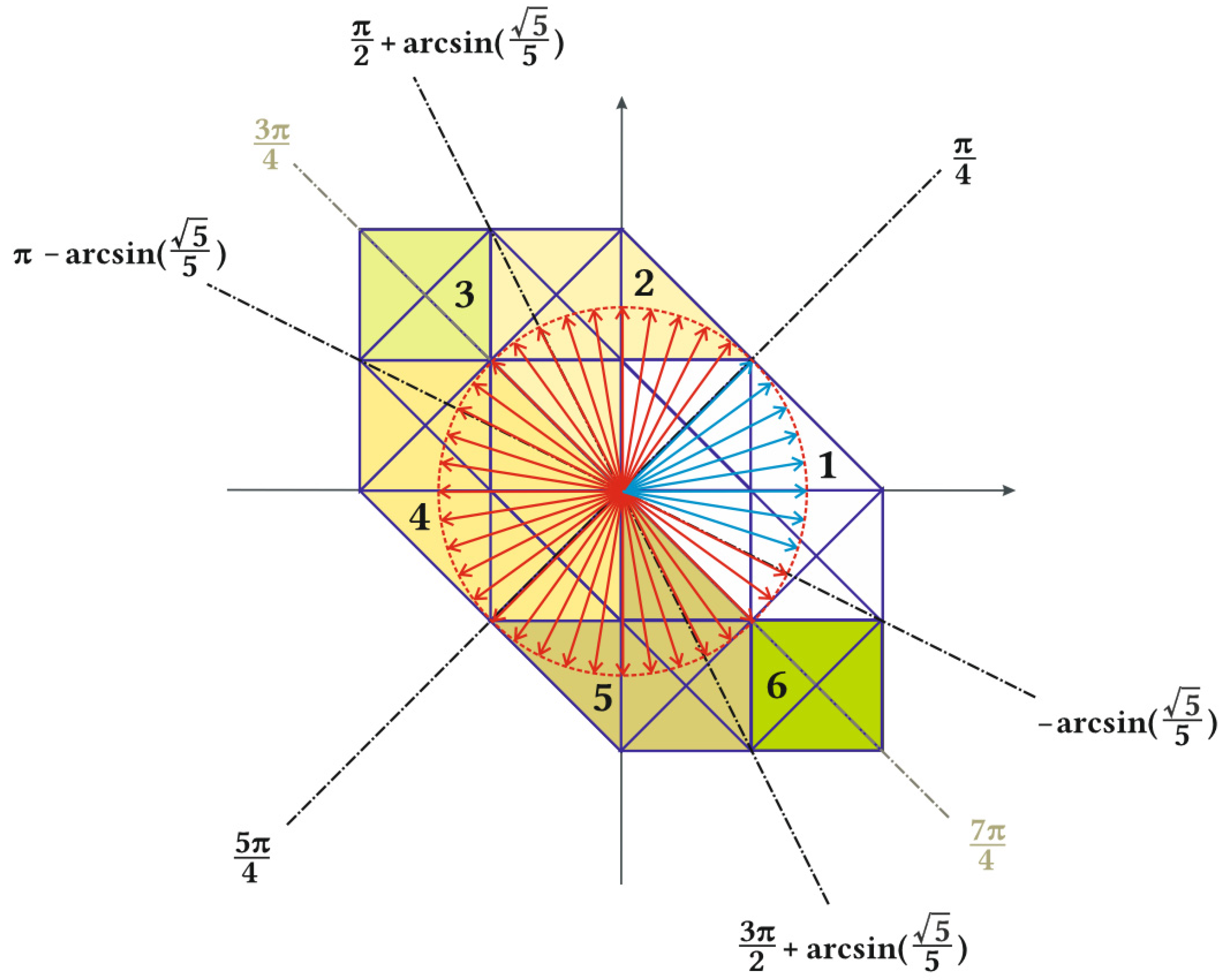
Figure 4.
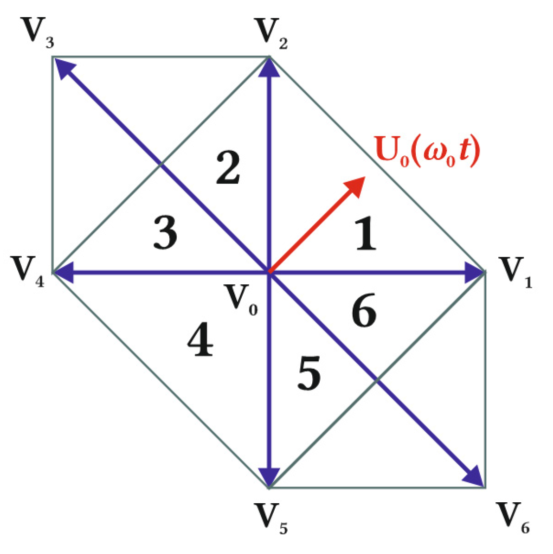
One zero vector and six active voltage vectors of a two-level two-phase NPC inverter with three legs. U0 represents the rotating magnetic field and is used as a reference voltage vector. U0 is synthesized by the proper sequence of V0, V1, and V2 vectors. The vectors create a hexagon that is divided into six sectors.
Figure 4.
One zero vector and six active voltage vectors of a two-level two-phase NPC inverter with three legs. U0 represents the rotating magnetic field and is used as a reference voltage vector. U0 is synthesized by the proper sequence of V0, V1, and V2 vectors. The vectors create a hexagon that is divided into six sectors.
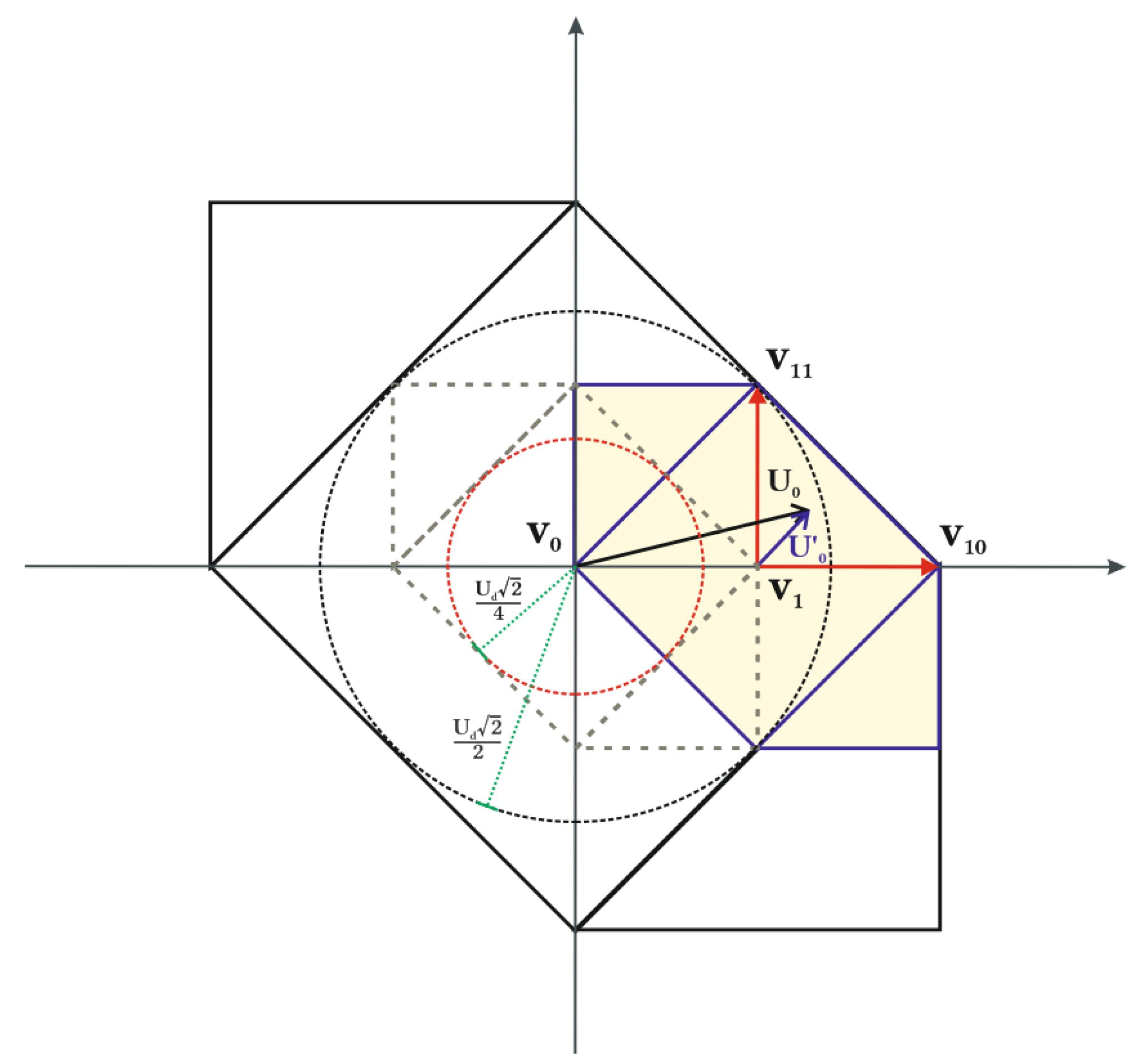
Figure 5.
Transposition of U0 coordinates to one of outer two-level hexagons, which gives the U’0. After the transposition, V1 vector is the local 0 vector. U’0 is synthesized by a combination of V1, V10, and V11 as in a two-level inverter. The outer circle represents the maximum modulation depth without overmodulation, and the inner circle represents half of the modulation depth.
Figure 6.
Transposition borders used for transposition of U0 vector. The red circle marks the limit of maximum modulation. Red and blue denote all discrete positions of U0 for 50 Hz, full modulation, and Tc = 500 μs. Positions of U0 marked in blue are transposed to the first outer two-level hexagon. The alternative transposition borders are marked green.
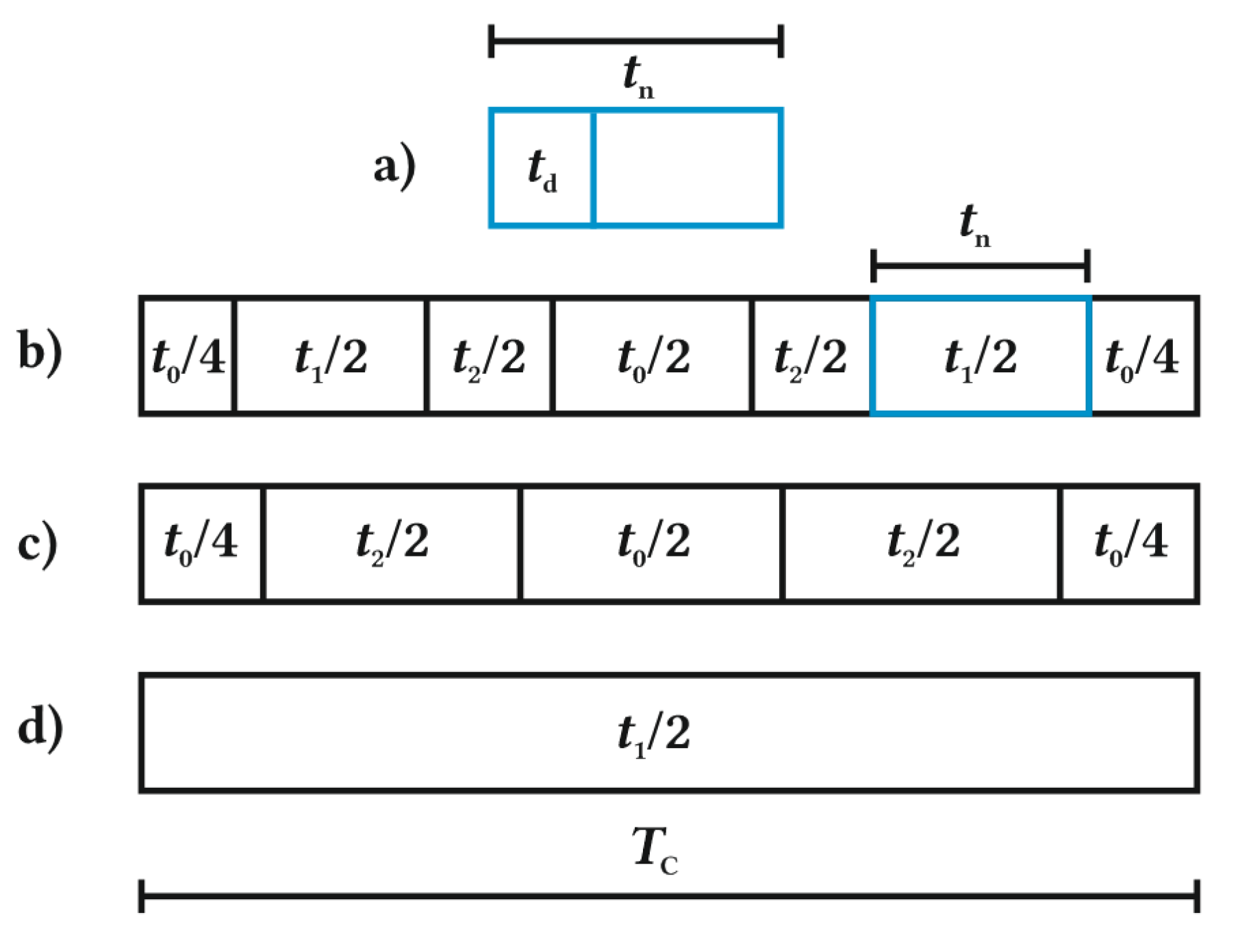
Figure 7.
Voltage vector switching sequence within a Tc sampling period.
Figure 7.
Voltage vector switching sequence within a Tc sampling period.
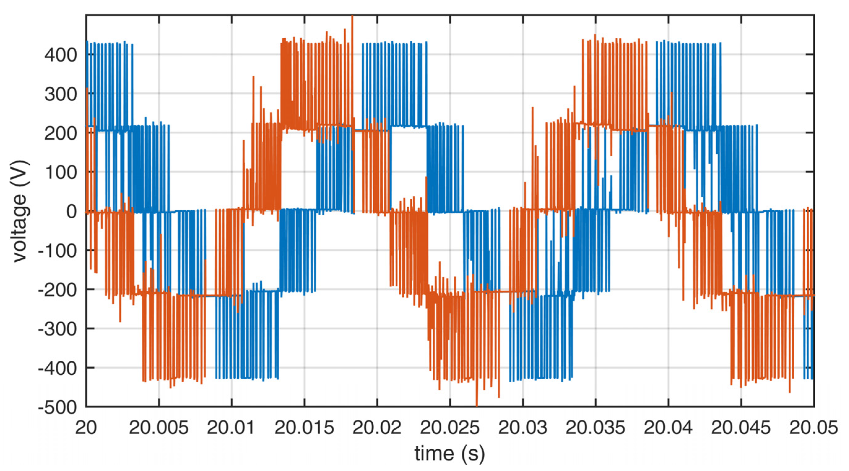
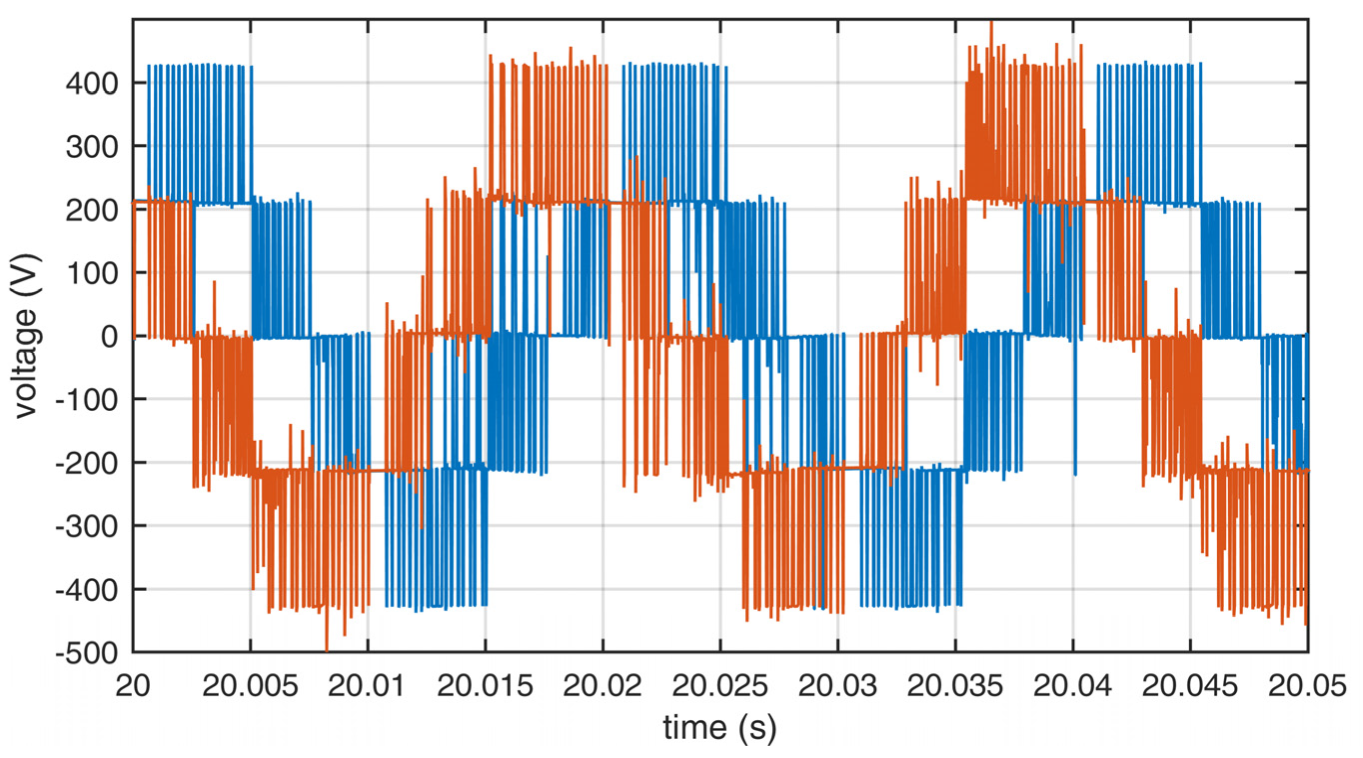
Figure 8.
Output line voltages of the inverter using set A. Blue—L1, red—L2.
Figure 8.
Output line voltages of the inverter using set A. Blue—L1, red—L2.
Figure 9.
Output line voltages of the inverter using set B. Blue—L1, red—L2.
Figure 9.
Output line voltages of the inverter using set B. Blue—L1, red—L2.
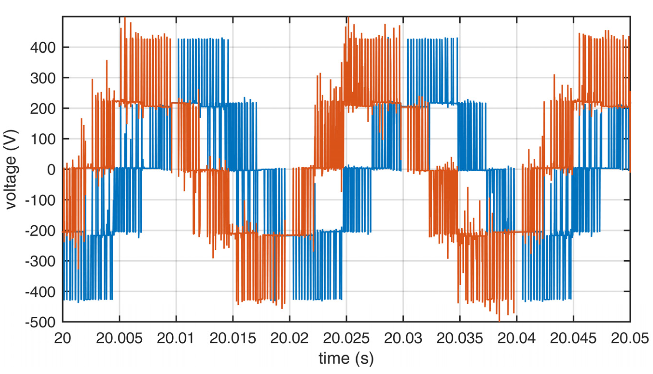
Figure 10.
Output line voltages of the inverter using set C. Blue—L1, red—L2.
Figure 10.
Output line voltages of the inverter using set C. Blue—L1, red—L2.
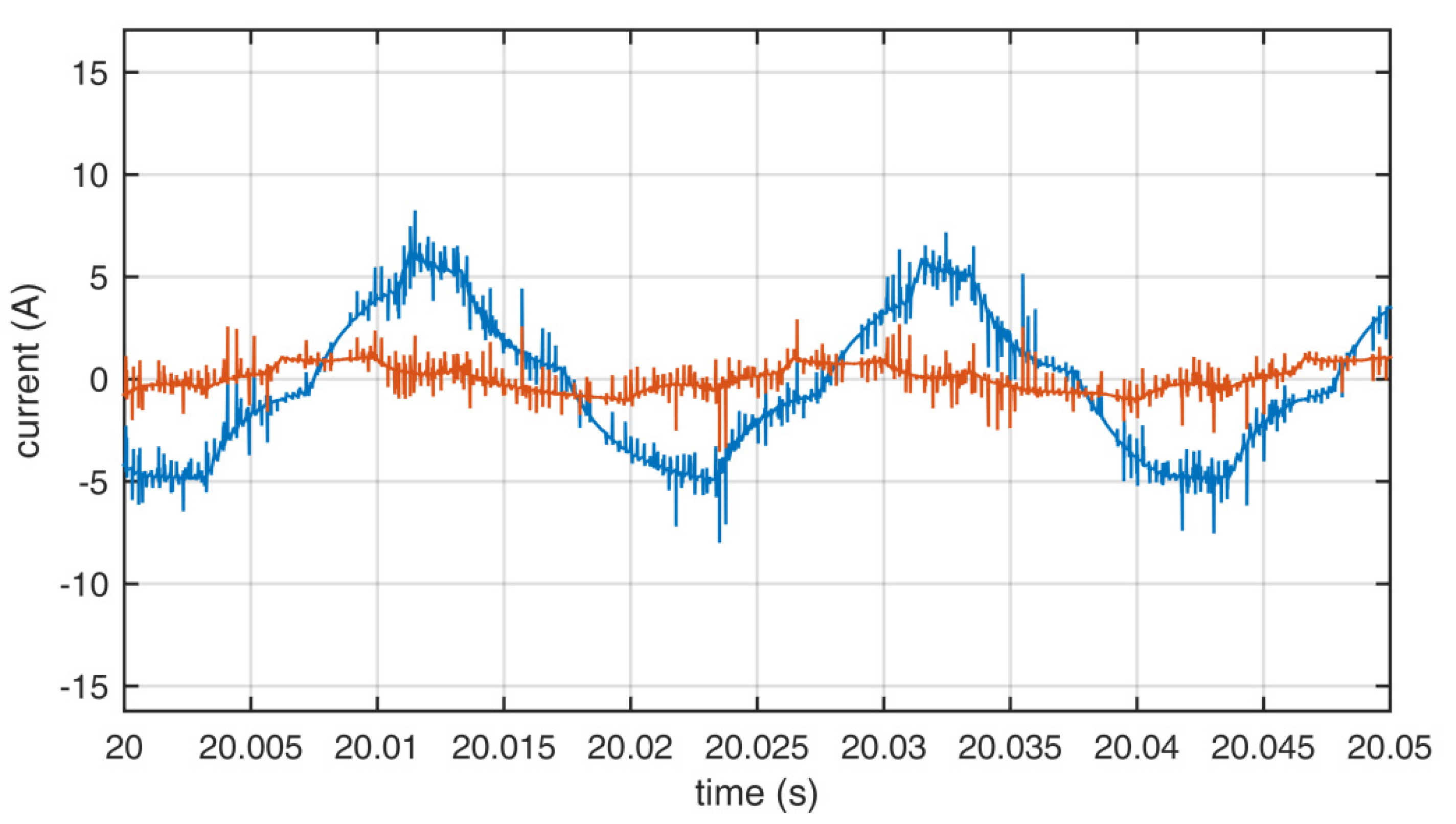
Figure 11.
Output currents of the inverter using set A. Blue—L1, red—L2.
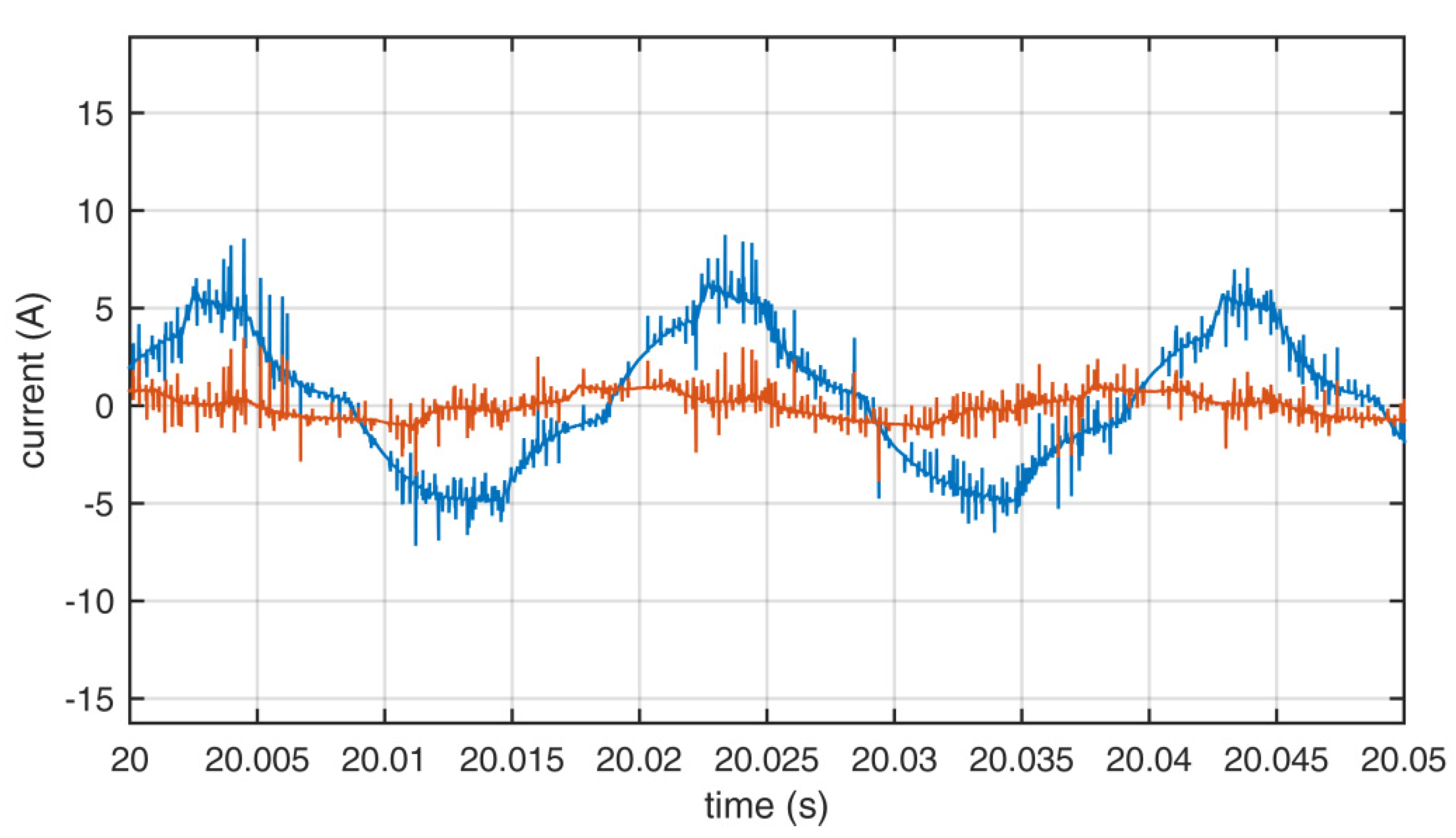
Figure 11.
Output currents of the inverter using set A. Blue—L1, red—L2.
Figure 12.
Output currents of the inverter using set B. Blue—L1, red—L2.
Figure 12.
Output currents of the inverter using set B. Blue—L1, red—L2.
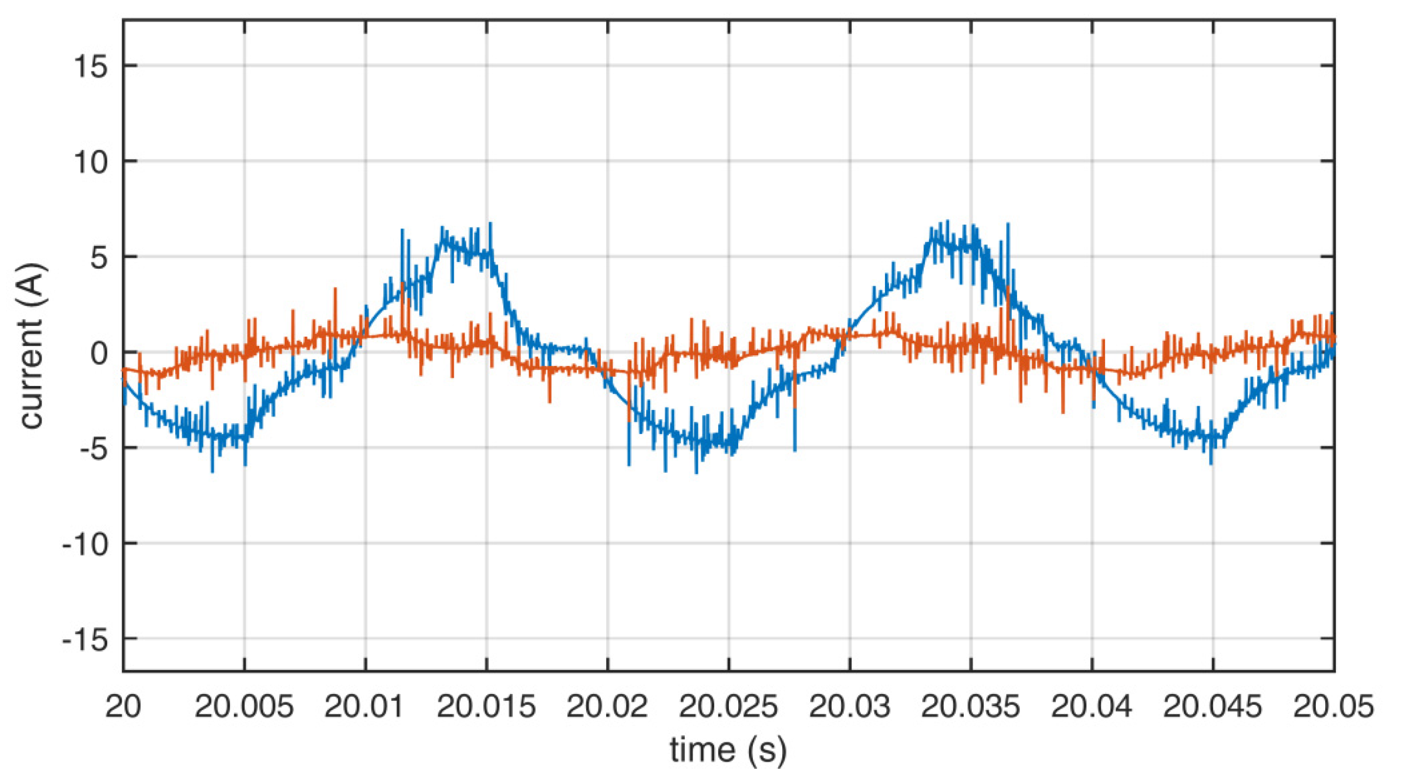
Figure 13.
Output currents of the inverter using set C. Blue—L1, red—L2.
Figure 13.
Output currents of the inverter using set C. Blue—L1, red—L2.
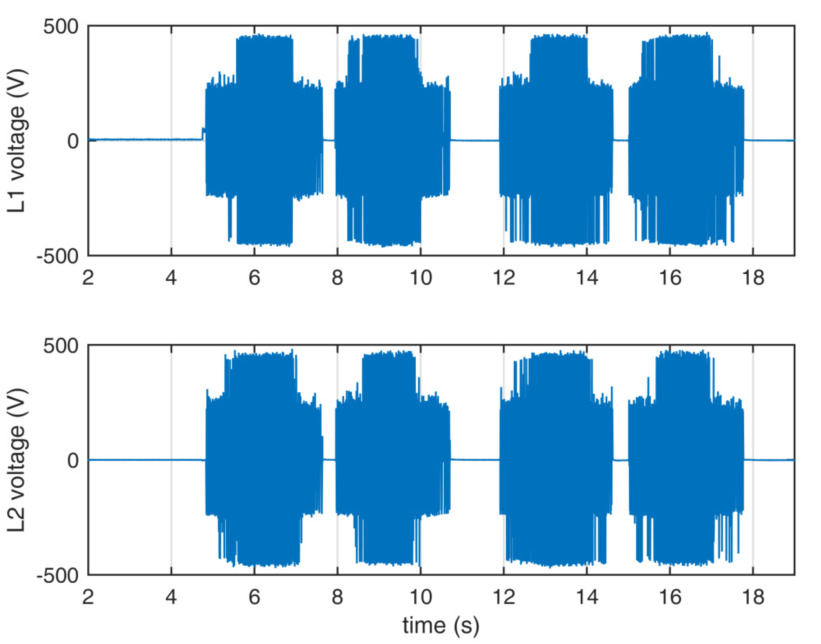
Figure 14.
Voltage waveforms of the dynamic state. The first half of the measurement uses set A, while the other half uses set C.
Figure 14.
Voltage waveforms of the dynamic state. The first half of the measurement uses set A, while the other half uses set C.
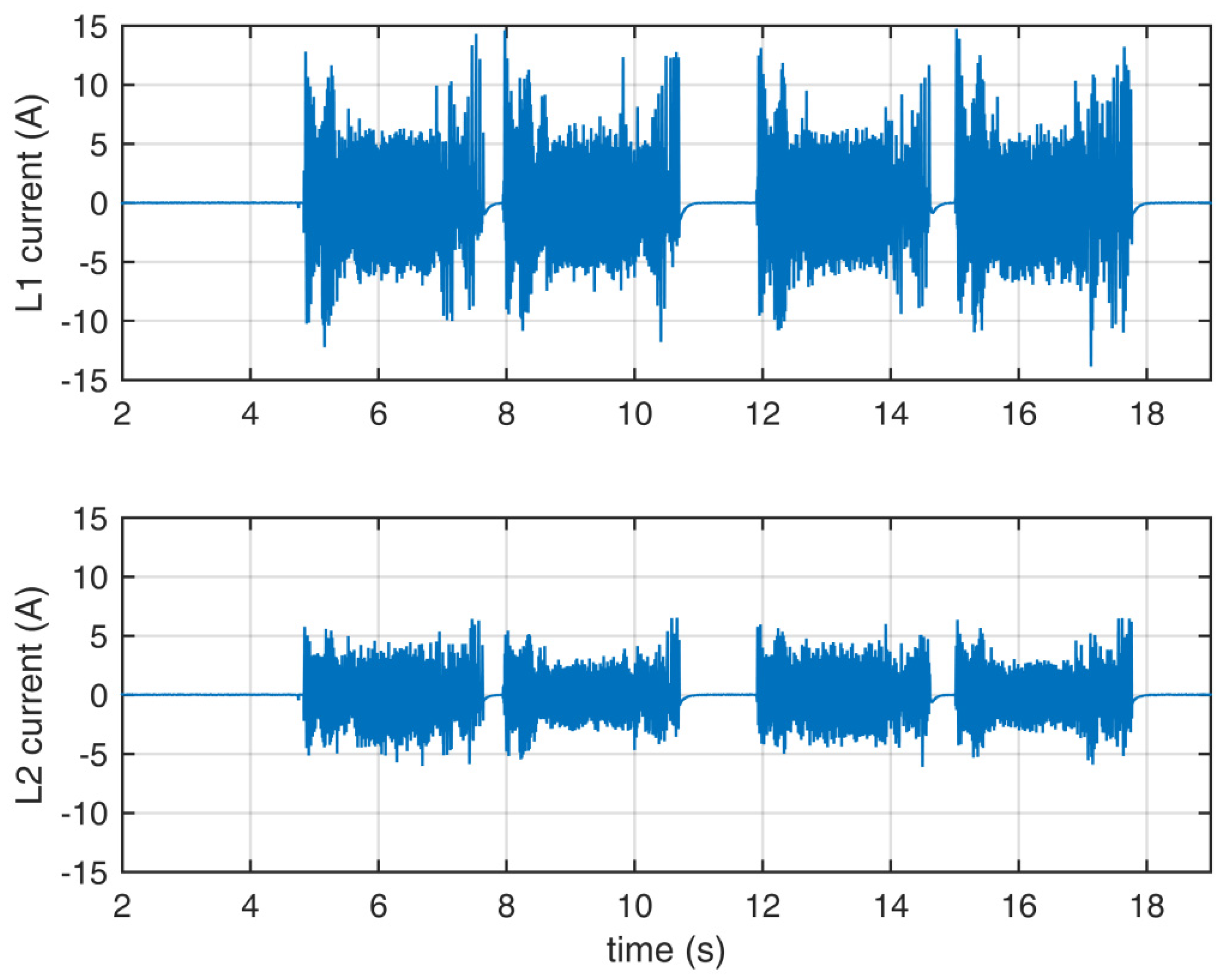
Figure 15.
Current waveforms of the dynamic state. The first half of the measurement uses set A, while the other half uses set C.
Figure 15.
Current waveforms of the dynamic state. The first half of the measurement uses set A, while the other half uses set C.
Table 1.
The switching states of the 3L-NPC inverter corresponding to the voltage vectors. The switching states are described as a 12-bit number in T1–T12 order; 0—OFF, 1—ON, *—loads C2, **—loads C1. Vectors V10 to V21 load all capacitors. Black—commonly used switching states of redundant voltage vectors; blue and orange—additional switching states; orange—switching states that do not allow flow of current both in and out of the neutral phase leg of the inverter.
| Vector Number | Vector Designation | Switching State | Vector Number | Vector Designation | Switching State |
|---|
| 1 | V0 | 110011001100 | 6 | V5 | 001100110110 * |
| 011001100110 | 011001101100 ** |
| 001100110011 | 001100110100 * |
| | 001000101100 ** |
| 011000101100 ** |
| 001001101100 ** |
| 2 | V1 | 011000110011 * | 7 | V6 | 011000110110 * |
| 110001100110 ** | 110001101100 ** |
| 010000110011 * | 010000110100 * |
| 110000100010 ** | 110000101100 ** |
| 110001100010 ** | 011000110100 * |
| 110000100110 ** | 010000110110 * |
| 3 | V2 | 011001100011 * | 8 | V10 | 110000110011 |
| 110011000110 ** | 9 | V11 | 110001100011 |
| 010001000011 * | 10 | V12 | 110011000011 |
| 110011000010 ** | 11 | V13 | 011011000011 |
| 011001000011 * |
| 010001100011 * |
| 4 | V3 | 011011000110 ** | 12 | V14 | 001111000011 |
| 001101100011 * | 13 | V15 | 001111000110 |
| 001011000010 ** | 14 | V16 | 001111001100 |
| 001101000011 * | 15 | V17 | 001101101100 |
| 011011000010 ** |
| 001011000110 ** |
| 5 | V4 | 011011001100 ** | 16 | V18 | 001100111100 |
| 001101100110 * | 17 | V19 | 011000111100 |
| 001011001100 ** | 18 | V20 | 110000111100 |
| 001101000100 * | 19 | V21 | 110000110110 |
| 001101100100 * |
| 001101000110 * |
Table 2.
Equations for t1 and t2 for every sector of two-level hexagon. ϑ is the angle, and ρ is the magnitude of U0 vector in polar coordinates.
Table 2.
Equations for t1 and t2 for every sector of two-level hexagon. ϑ is the angle, and ρ is the magnitude of U0 vector in polar coordinates.
| Sector Number | t1 | t2 |
|---|
| 1 | Tc ρ cos(ϑ) | Tc ρ sin(ϑ) |
| 2 | −Tc ρ cos(ϑ) | Tc ρ (cos(ϑ) + sin(ϑ)) |
| 3 | Tc ρ sin(ϑ) | −Tc ρ (cos(ϑ) + sin(ϑ)) |
| 4 | −Tc ρ sin(ϑ) | −Tc ρ cos(ϑ) |
| 5 | −Tc ρ (cos(ϑ) + sin(ϑ)) | Tc ρ cos(ϑ) |
| 6 | Tc ρ (cos(ϑ) + sin(ϑ)) | −Tc ρ sin(ϑ) |
Table 3.
Calculation of the transition from the current state of transistors to a possible version of the next voltage vector in a sequence in search of the smallest switching number.
Table 3.
Calculation of the transition from the current state of transistors to a possible version of the next voltage vector in a sequence in search of the smallest switching number.
| Current State | Possible Next State | XOR | Number of Changes |
|---|
| 110001100011 | 011000110011 | 101001010000 | 4 |
| 110001100011 | 110001100110 | 000000000101 | 2 |
| 110001100011 | 010000110011 | 100001010000 | 3 |
| 110001100011 | 110000100010 | 000001000001 | 2 |
| 110001100011 | 110001100010 | 000000000001 | 1 |
| 110001100011 | 110000100110 | 000001000101 | 3 |
Table 4.
Calculation of the dead-time transition state.
Table 4.
Calculation of the dead-time transition state.
| Current State | Next State | Transition State |
|---|
| 110001100011 | 110001100110 | 110001100010 |
| 110001100011 | 110000100010 | 110000100010 |
Table 5.
The list of main components of the prototype inverter.
Table 5.
The list of main components of the prototype inverter.
| Component | Name |
|---|
| IGBT modules | Infineon FS150R12KE3G, VCE = 1200 V, ICnom = 150 A |
| NPC diodes | IXYS Dsei2x101-12a, VRRM = 1200V, IF = 99 A |
| Filtering capacitors | Kemet ALS70A332MF500, 3300 µF, 500 V |
| Bridge rectifier | Vishay VS-90MT120KPBF, VRRM = 1200 V, IO = 90 A, IFSM = 770 A |
| Digital signal controller | TMS320F28379D |
Table 6.
THD of output voltages and currents of the inverter—1 s window.
Table 6.
THD of output voltages and currents of the inverter—1 s window.
| | Set A | Set B | Set C |
|---|
| L1 voltage | 7.20% | 7.96% | 7.27% |
| L2 voltage | 6.15% | 7.45% | 6.69% |
| L1 current | 6.51% | 6.91% | 6.31% |
| L2 current | 10.70% | 11.46% | 11.39% |
Table 7.
The switching number for 2 s of full modulation, 50 Hz.
Table 7.
The switching number for 2 s of full modulation, 50 Hz.
| | Set A | Set B | Set C |
|---|
| Switchings | 63,526 | 45,383 | 51,461 |
| % of reduction | − | 28.56% | 18.99% |


