1. Introduction
Nowadays, renewable energy sources, among which photovoltaic (PV) plants play an important role, are of paramount importance, and they are attracting the attention of researchers to reduce pollution and increase the production of green energy.
PV plants usually comprise several PV modules that can be connected in series to augment the total output voltage composing the PV strings. The latter can be connected in parallel, forming different PV arrays that constitute the entire PV plant, thereby increasing both the total output current and the total output power. In the literature, it is possible to find many solutions to interface PV plants with the electrical network [
1]. One of the simplest and most common is composed of a DC–DC converter and a central inverter. The former connects the PV plant to the central inverter and extracts the maximum available power through centralized maximum power point tracker (CMPPT) algorithms [
2,
3], while the latter connects the PV plant to the grid. On the other hand, under unbalanced irradiance conditions (partial shading), the shaded PV modules, being connected to the same DC–DC converter, could limit the power production of the entire string or array. Even though dedicated algorithms for inhomogeneous irradiance conditions are proposed in the literature [
4,
5,
6], the maximum achievable power is still lower than the sum of the maximum power obtainable by the individual PV modules. To further increase the overall efficiency of a PV plant, it is possible to adopt distributed maximum power point tracker (DMPPT) algorithms. The latter can be implemented through dislocating different converters (such as microinverters or DC–DC converters) controlling the different PV arrays, strings, or modules [
7,
8]. In this way, each PV subgroup can operate at its maximum power point, but the total cost of the plant increases. Another possible solution, particularly used in medium- and high-voltage systems, is based on the exploitation of the topology of the modular multilevel converter (MMC). On the other hand, the latter solution can also be used in low-voltage systems to take advantage of the MMC’s intrinsic benefits, such as modularity, redundancy, high voltage quality, and lower power losses [
9].
PV modules are subjected to degradation due to high voltage stress, and they can usually withstand insulation voltages of up to 1–1.5 kV. In the case of medium- and high-voltage systems, the need for galvanic isolation arises. This can be ensured using internal DC–DC converters based on high-frequency transformers, such as flyback and dual active bridge converters, connected to each submodule (SM) of the MMC [
10,
11,
12,
13].
In any case, different solutions to interface many PV modules/strings/arrays based on MMC were proposed and analyzed in the literature. It is possible to interface the whole PV system to the DC side of the MMC, as reported in [
14], interface the PV subgroups to each SM of the MMC through dedicated DC–DC converters, as reported in [
15,
16], or directly to the submodule capacitors of the MMC, as reported in [
17,
18], for low-voltage systems. On the other hand, in [
14], the same issues of the central inverter structure occur. In [
15,
16,
17,
18], a DMPPT tracker could be adopted with the advantages related to that solution. However, the internal converter power mismatch should be opportunely managed under partial shading conditions. In particular, in [
17], redundant submodules of the MMC were used to compensate for internal converter power mismatches, while in [
16], the authors proposed a control strategy based on using both the AC and DC circulating currents to balance the power mismatches in the whole MMC, avoiding the usage of redundant submodules. On the other hand, because of the converter topology, the three legs of the MMC are not independent each other since the absence of a current reclosure through the DC side. Therefore, even under unbalanced irradiance conditions between the arms of only one leg, the other two legs of the MMC are also interested in reactive circulating currents for the current reclosure; thus, higher AC circulating voltages can be required to drive these currents, and more converter losses can occur.
To overcome these issues and reduce converter complexity, in [
19], the authors proposed a novel control strategy for a single-phase MMC that laid the foundations for the low-voltage three-phase MMC topology proposed in [
20]. In both topologies, the PV arrays were directly connected to the capacitors of MMC submodules. In the three-phase topology [
20], an additional larger capacitor was connected to the DC side of the MMC. In this way, it was possible to decouple the three legs of the MMC. In fact, in case of unbalanced irradiance conditions between the arms of only one leg, the AC circulating currents can flow through the capacitor of the DC side without interesting the other legs of the MMC; thus, the total system efficiency can increase. On the other hand, in [
20], the sizing of that DC-side capacitor and its influence on system performance are missing.
In the present work, a comparison of the control strategy reported in [
20] in the presence of a DC-side capacitor with respect to the one reported in [
16] without a DC-side capacitor is performed, focusing on AC circulating voltage management and converter losses. Specifically, the quantification of the real benefits of the use of an additional DC-side capacitor is pointed out. Lastly, an optimal sizing procedure of such a capacitor is proposed to optimize the AC circulating voltages and minimize converter losses. Its effectiveness is demonstrated by means of numerical simulations in the Matlab/Simulink environment.
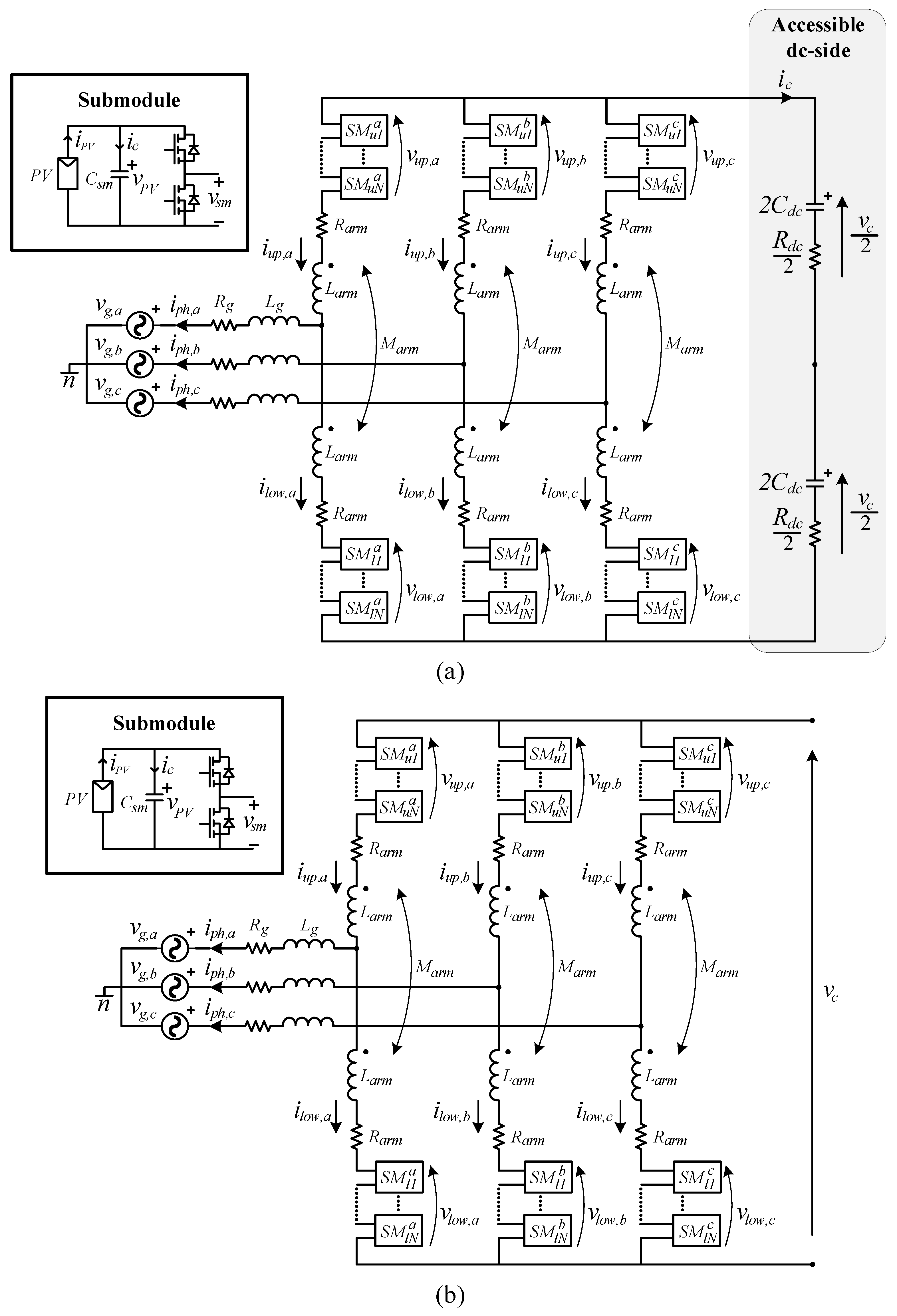
2. Converter Topologies
The analyzed converter topologies are reported in
Figure 1. They are related to the control strategy reported in [
20], in the presence of the DC-side capacitor (
Figure 1a), and to the control strategy reported in [
16], without the DC-side capacitor (
Figure 1b). Both consist of three legs, one per phase, and, in turn, each leg is made up of two arms, i.e., the upper and lower arm, connected through mutually coupled inductors. Then, each arm is based on the cascade connection of
N submodules based on the half-bridge topology. The PV arrays are directly interfaced through the SM capacitors, enabling a fully distributed system. The distinction between the two topologies is based on the presence of an additional reclosure path for the AC circulating currents due to the inclusion of a DC-side capacitor in the converter topology shown in
Figure 1a.
The equations governing both converter topologies can be derived from
Figure 1. To simplify the model related to the topology of
Figure 1a, two series-connected capacitors are depicted. However, in the real system, only one capacitor is required. In both cases, when considering the equivalent single-phase circuit and applying Kirchhoff’s voltage law to a loop that includes a generic
k-th phase (with
k ∈ {
a,
b,
c}) of the converter and the DC side, and assuming that the converter control does not introduce any homopolar voltage component, ensuring that the middle point of the DC side and the AC neutral point are at the same potential, the voltages of the upper and lower arms can be expressed as follows:
where
vup,k and
vlow,k are the upper and lower arm voltages of the
k-th phase, respectively,
vg,k is the grid voltage of the
k-th phase,
vc is the voltage of the DC-side,
Rarm is the arm resistance,
Larm is the arm inductance,
Marm is the mutual arm inductance,
Rg is the grid resistance, and
Lg is the grid inductance. Lastly,
iup,k and
ilow,k are the upper and lower arm currents, respectively. Moreover, the output phase grid currents can be derived from Kirchhoff’s current law applied at the output AC terminals as follows:
while the circulating currents are defined as
The output phase grid currents allow us to exchange electric power with the grid, while the circulating currents manage the internal converter energy. These current components are driven by the related components of the arm voltages. Indeed, the latter can be rewritten to emphasize the grid and circulating components as follows:
where
vph,k is the output phase grid voltage component and
vcirc,k is the circulating voltage component of the
k-th phase. The output phase grid voltages,
vph,k, are supposed to be composed of just AC components,
, while the circulating voltages necessary to drive the related circulating currents are derived as follows:
The analyzed converters, which comprise several PV panels connected in such a way to achieve a fully distributed system, can be characterized by internal power mismatches among the converter legs and arms. To deal with partial shading conditions, AC and DC circulating currents, composed of positive-, negative- and zero-sequence components, need to be generated [
16,
19,
20]. Therefore, the corresponding circulating voltages are defined as follows:
where
and
are the AC and DC circulating voltage components, respectively,
and
are the AC and DC circulating current components, while
and
Vdc are the AC and DC voltage components of the DC side. It is important to note that in the topology without the DC-side capacitor, the voltage
is zero.
In particular, the AC circulating components are used to handle power mismatches between the arms belonging to the same converter phase, while the DC circulating components are used to manage power mismatches among the converter legs, always ensuring balanced power injection into the grid. In this regard, in the topology with the DC-side capacitor, the latter plays a crucial role in managing power mismatches between the arms, facilitating the control of AC circulating currents. Indeed, in cases where the DC-side capacitor is absent, the converter phases are coupled to each other, potentially leading to the generation of active and reactive AC circulating current components depending on the unbalanced conditions.
In contrast, through adding a DC-side capacitor, the converter phases can be decoupled, allowing for the generation of only active AC current components, and consequently reducing power losses. Additionally, as shown in Equation (6), in both cases, the AC component of the DC-side voltage is directly related to the AC circulating voltages. Therefore, the DC-side capacitor can be appropriately sized to better manage the circulating voltages required for handling the internal power mismatches between the arms through minimizing and equalizing their values as much as possible. In this case, the DC-side voltage can be evaluated as
where
vc(0) is the initial voltage value of the DC-side capacitor,
ic is the DC-side current, and
Cdc is the capacitance of the DC-side capacitor. This DC-side current depends on the injected AC circulating currents and DC transient component. The latter under steady state condition is nil and, thus, the AC component is given by:
Therefore, the DC-side voltage consists of the AC component related to the flow of the AC circulating currents and the DC component Vdc. The latter is necessary because the SMs of the MMC are based on a half-bridge topology, and then the arms can synthesize only positive voltages. In the case of the converter topology without the DC-side capacitor, (7) does not apply, and the sum of the three AC circulating currents of (8) becomes zero.
3. AC Circulating Power Flow Analysis
As mentioned in the previous section, for both converter topologies, the AC circulating currents must flow through the converter under unbalanced irradiance conditions between two arms of the same leg. On the other hand, the DC circulating currents must flow through the converter under unbalanced irradiance conditions among the legs. These allow each arm to deliver the maximum available power.
The presence of the DC-side capacitor enables the decoupling of AC circulating current control without affecting DC circulating current control. Therefore, in this section, the MMC power flow analysis primarily focuses on AC circulating currents.
In both converter topologies, the AC circulating currents are directly linked to the instantaneous power mismatch between the arms, which are defined, as reported in [
16], as follows:
Considering, separately for each
k-th converter phase, the output phase grid voltage,
vph,k, as the reference frame and applying the Hilbert transform, each of the three AC circulating currents can be decomposed into their own direct and quadrature components,
and
, respectively, [
21]. Therefore, (9) can be rewritten as follows:
where
is the amplitude of the output phase grid voltage. The latter is supposed to consist only of the positive-sequence component. The direct components of the AC circulating currents are related to the arm active power mismatches,
Pd,k, and the quadrature components of the AC circulating currents are related to the arm reactive power mismatches,
Qd,k.
When considering the phasors of the positive-, negative-, and zero-sequences of the AC circulating currents, each AC circulating current can be defined over time as
where
m = 1, 2, 3 for
k =
a,
b,
c, respectively;
are the amplitudes of the positive-, negative-, and zero-sequences, respectively; and
are the phase displacement of the positive-, negative-, and zero-sequences of the AC circulating currents with respect to the positive sequence of the output phase grid voltages. The arm active and reactive power mismatches can be evaluated based on (9) and (11) as
It is worth noting that, while arm active power mismatches, Pdk, are solely influenced by unbalanced irradiance conditions, arm reactive power mismatches, Qdk, can vary depending on the control strategy employed for AC circulating current control.
In the converter topology with the presence of the DC-side capacitor, the arm reactive power mismatches can always be zero under any unbalanced irradiance conditions. This is possible because the quadrature components of the AC circulating currents can be separately controlled to be zero.
Conversely, in the converter topology without the presence of the DC-side capacitor, the arm reactive power mismatches may not be zero, as the quadrature components of the AC circulating currents cannot be separately controlled.
In light of the above, the MMC power flow analysis, related to the AC circulating currents, is conducted for the control algorithm proposed in [
20] in the presence of the DC-side capacitor, referred to as the decoupled power mismatch elimination (DPME) control strategy, and the control algorithm proposed in [
16] without the presence of the DC-side capacitor, referred to as the coupled power mismatch elimination (CPME) control strategy.
3.1. DPME Control Strategy
This control strategy is proposed, analyzed, and validated in [
20]. From that analysis, the three phasors of the AC circulating currents can be defined as:
where
and
are the reference
d-components of the AC circulating currents, which depend on the unbalanced irradiance conditions. The reference
q-components of the AC circulating currents,
, are imposed to be nil to maximize the converter efficiency. In this way, the AC circulating currents involve only an active power exchange between the arms. Therefore, the sum of the three circulating currents can be non-zero and will flow through the DC-side capacitor. Applying the Fortescue transform to (13), the phasors of the positive-, negative-, and zero-sequences of the AC circulating current references are given by
It is worth noting that, according to (14), the DPME control strategy assumes that, regardless of the irradiance conditions, the three AC circulating currents must be 60° or 120° apart from each other, according to the direction of the arm active power mismatches. As a result, the phasors of the negative- and zero-components result in the complex conjugate of the other, i.e.,
and
. Each AC circulating current can be defined over time as the sum of the positive-, negative-, and zero-sequences, as follows:
The arm active
Pd,k and reactive
Qd,k power mismatches can be evaluated from (13) and (15) as
Therefore, taking the amplitude of the positive AC circulating currents and the real and imaginary parts of the negative AC circulating currents as unknown variables, it is possible to invert (16) and obtain, in a matrix form, the following:
For each value of the arm active power mismatches
Pd,a,
Pd,b,
Pd,c, it is possible to determine the positive-, negative-, and zero-sequence references of the AC circulating currents, which allow each arm producing the maximum available power under any irradiance condition. Applying the inverse Fortescue transform to (17), the phasors of the AC circulating currents,
, are as follows:
Looking at the equivalent circuit of the AC circulating components in the phasor domain shown in
Figure 2, the phasors of the AC circulating voltages generated by each
k-th converter leg,
, can be retrieved for the DPME control strategy as follows:
where
is the phasor of the AC component of the capacitor current and
where
is the equivalent internal impedance of each converter leg and
is the DC-side capacitor impedance. The leg impedance,
, depends on the arm inductor resistance,
Rarm; inductance,
Larm; and mutual coupling,
Marm; while the DC-side capacitor impedance depends on its equivalent series resistance,
Rdc, and its capacitance,
Cdc.
Lastly, through solving (18), the AC circulating currents can be computed, and the power losses due to such currents can be derived as follows:
where
(with
k ∈ {
a,
b,
c}) are the amplitudes of the AC circulating currents and
is the amplitude of the AC current component flowing in the DC side. It is worth noting that, since the analysis between the DPME and CPME control strategies is focused on the fundamental AC circulating components needed to face arm partial shading conditions, only such current components were considered for the power loss evaluation.
3.2. CPME Control Strategy
This control strategy is proposed, analyzed, and validated in [
16]. From that analysis, the matrix that links the arm power mismatches and the phasors of the AC circulating current sequences are as follows:
where
Qd represents the sum of the reactive arm power mismatches. Although
Qd can be forced to be zero for maximizing the converter efficiency, the reactive power exchange in each converter phase may not be zero due to the coupling of the converter legs, which differs from the DPME algorithm. The matrix linking the arm power mismatches and phasors of the AC circulating currents is as follows:
In this case, the zero-sequence component of the AC circulating currents is forced to be zero (no DC-side capacitor). For instance, in case there is an arm active power mismatch in just one converter leg, unlike in (18), the circulating currents of the other two legs will not be zero. Specifically, they will be phase-shifted by about 90° with respect to their related output phase grid voltages, involving just an exchange of reactive power.
Unlike the DPME control strategy, the phasors of the AC circulating voltages,
, generated by each
k-th converter leg adopting the CPME control strategy, depend only on the leg impedance, and they can be retrieved as follows:
Lastly, the relationship between the arm active power mismatches and AC circulating currents can be retrieved from (23). Then, the power losses due to solely the fundamental AC circulating components are as follows:
4. Proposed DC-Side Capacitor Sizing Procedure and Comparison between DPME and CPME Control Strategies
This section outlines the sizing procedure for the DC-side capacitor of the DPME control strategy. Additionally, a comprehensive comparison with respect to the CPME control strategy is conducted to evaluate the required AC circulating components and their impact on the converter operation. This analysis aims to identify the actual advantages of the MMC topology with the additional DC-side capacitor.
4.1. Proposed DC-Side Capacitor Sizing Procedure
The proposed sizing procedure for the DC-side capacitor of the DPME control strategy aims to achieve the following goals: (i) minimize the required AC circulating voltages; (ii) minimize the deviation in those voltages among the three phase converter legs (referred to as voltage equalization); (iii) minimize overall power losses. These goals are related to the three metrics
Jv,max,
Jv,eq, and
Jloss, respectively, which are defined as follows:
where
M is the total number of the considered combinations of arm active power mismatches,
p(
m) is the probability of the
m-th power mismatch combination,
Vdc,n is the rated DC-side voltage at the maximum irradiance condition,
Pcirc represents the power losses due to the AC circulating currents, and
Pn is the rated power plant.
In particular, the minimization of the maximum AC circulating voltages, Jv,max, can help avoid oversizing the number of the converter SMs or excessively increasing the rated SM voltages. Indeed, the amplitude of the AC circulating voltages directly affects the required upper and lower arm voltages to be synthesized by the MMC.
The equalization of the AC circulating voltages can be useful to reduce the deviation among the three voltages, Jv,dev, and balancing the stress among the semiconductor devices of different legs.
Finally, the optimization procedure takes into account the influence of the equivalent series resistance of the DC-side capacitor,
Rdc, to minimize overall power losses,
Jloss. The capacitor resistance, at a fixed working frequency, can be expressed as a function of the capacitance as follows:
where tan
δ is the loss tangent of the capacitor, which can be obtained from the datasheet provided by a specific capacitor manufacturer.
The design of the DC-side capacitor was carried out through expressing its reactance
Xdc as a function of the leg reactance
Xleg as follows:
where α is the resonant factor. According to (19), in the case of the DPME algorithm, the reactance of the DC-side capacitor can decrease the equivalent internal converter leg impedance, thereby reducing the absolute value of the required AC circulating voltages. On the other hand, to minimize the power losses,
Jloss, the real parts of the impedances are considered in (21). As mentioned earlier, the DPME control strategy can have a positive impact on power losses. In the CPME control strategy, all converter legs are affected even if there is an arm active power mismatch in just one leg of the MMC. On the other hand, in the DPME control strategy, only the unbalanced converter legs will carry the required circulating currents, and they will close their path through the DC-side capacitor. Of course, the equivalent series resistance of the capacitor should be sufficiently low to minimize power losses under any irradiance conditions. In order to consider the influence of the capacitor resistance
Rdc, according to (27) and (28), it can be expressed as a function of leg reactance
Xleg. This allows all the metrics of (26), for given arm active power mismatches; leg impedance,
; capacitor impedance,
; DC-side voltage,
Vdc,n; and rated power plant,
Pn, to be expressed as a function of the resonant factor
α. Therefore, for each value of α, the three metrics can be evaluated. Finally, through combining these metrics with appropriate weight factors, it becomes possible to optimize the DC-side capacitor, assigning varying levels of importance to the minimization of the AC circulating voltages, their equalization, or reduction of power losses through evaluating the following cost function:
where
wv,max,
wv,eq, and
wloss are the weight factors related to each metric. Specifically, they range between 0 and 1, and their sum is equal to one. Therefore, considering a set of
H possible values of
α,
α ∈ {
α1, …,
αH}, the optimal value of the resonant factor
αopt can be obtained through minimizing the cost function
J(
α), i.e.:
The proposed DC-side capacitor sizing procedure can be summarized as follows:
- (1)
Define the rated MMC DC-side voltage, Vdc,n; the rated power plant, Pn; and leg impedance, Zleg.
- (2)
Define all possible combinations M of the arm active power mismatches and the probability of occurrence for the m-th power mismatch combination.
- (3)
Choose a capacitor technology and express its equivalent series resistance, Rdc, as a function of its reactance, Xdc, according to (27).
- (4)
Express the capacity reactance, Xdc, as a function of the leg reactance, Xleg, according to (28).
- (5)
Evaluate the AC circulating currents for each m-th power mismatch combination following (18).
- (6)
Evaluate the AC circulating voltages and power losses due to the AC circulating currents for each m-th power mismatch combination, following (19) and (21), respectively. They will be expressed as functions of the resonant factor α.
- (7)
Evaluate the three metrics Jv,max(α), Jv,eq(α), and Jloss(α) according to (26).
- (8)
Evaluate the cost function J(α) according to (29).
- (9)
Find the optimal value of the resonant factor, αopt, that minimizes the cost function J(α).
- (10)
Derive the optimal capacity reactance, Xdc, from (28).
- (11)
From among the available capacitors, choose the one with a capacitance value as close as possible to the optimal one. Since the capacitor should withstand the DC-side voltage, Vdc, a capacitor bank made of series- and/or parallel-connected capacitors could be required.
In real applications, the sizing procedure could be extended, performing a techno-economic analysis considering different aspects such as the costs, technologies, manufacturers of employable static switches and DC-side capacitors, and the number of the converter components. Indeed, the proposed sizing procedure defines three metrics related to converter efficiency, equalization of the stress on semiconductor devices, and oversizing the number of SMs along with their rated voltage. Therefore, employing different technologies and/or manufacturers for these components can result in different costs. In this extended analysis, an additional economic cost function that evaluates the total cost of each possible solution should be defined. This function should include the cost of the DC-side capacitor, the cost associated with the maximum required AC circulating voltage and their equalization that could lead to different numbers of converter components and/or sizes of semiconductor devices. Then, after defining the PV plant lifetime and the probability distribution of the possible arm active power mismatches, the total cost can be evaluated for each possible combination of wv,max, wv,eq, wloss, and α. The optimal solution is the one that minimizes the total cost. Finally, the latter total cost related to the optimal size of the DC-side capacitor obtained for the DPME control strategy can be compared with the one obtained for the CPME control strategy under the same conditions. This allows for an assessment to determine if adding a DC-side capacitor is justified from a techno-economic point of view. For instance, there may be small arm active power mismatches involving lower circulating currents, or even larger power mismatches that result in balanced circulating currents without any current flowing through the DC-side capacitor, for which the DC-side capacitor can be useless.
4.2. Comparison between DPME and CPME Strategies
The comparison was conducted through calculating the percentage improvements of the DPME control strategy compared to the CPME one. This was carried out through computing the ratios between the metrics Jv,max, Jv,dev, and Jloss for the two control strategies and considering the sum of the arm reactive power mismatches, Qd, nil for the CPME control strategy.
For a comprehensive comparison, we decided to consider various combinations of arm active power mismatches, Pd,k, running from -Pmax to Pmax with a step of 0.1Pmax. It is worth noting that, according to (9), Pmax is achieved when only one arm is producing the maximum power while the other arm of the same leg remains idle.
It is important to note that when evaluating these ratios, the rated DC-side voltage, Vdc,n; rated power plant, Pn; and Pmax are simplified, making this comparison independent of these values. On the other hand, the probability density function chosen for arm active power mismatch combinations, as well as the values of leg and capacitor impedance, are not simplified. As a result, this comparison depends on these specific values and should be conducted for the specific case under study.
However, for a comprehensive comparison, we decided to assume a uniform probability density function. Moreover, it is possible to demonstrate that if the real part of the impedances Zleg and Zdc in (19) and (24) is neglected, and the ratios of the metrics Jv,max and Jv,eq for the two control strategies are performed considering (28), the Xleg terms are simplified. This assumption is reasonable because, often, the reactance terms are higher than the related resistance terms. As a result, these ratios depend solely on the percentage of arm active power mismatches and resonant factors.
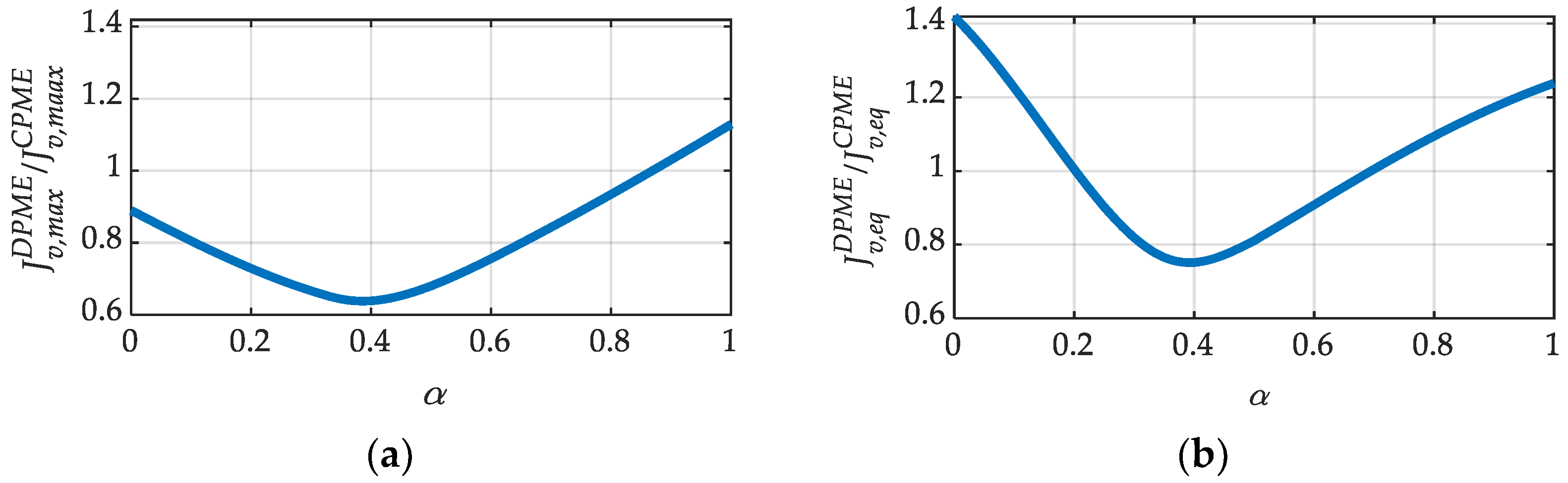
For all these combinations, the values of the AC circulating voltages were calculated for both the DPME and CPME control strategies using (19) and (24), respectively. This procedure was performed through varying the resonant factor α from 0 to 1 with a step of 0.01 for
Jv,max and
Jv,eq in the case of the DPME control strategy. It is worth noting that, for the CPME control strategy, the metrics of (26) can be evaluated for the different considered combinations of power mismatches, but they do not depend on the resonant factor. The results are shown in
Figure 3.
Looking at
Figure 3a, it is worth noting that the DPME control strategy requires lower AC circulating voltages compared to the CPME control strategy for α lower than 0.87. On the other hand, looking at
Figure 3b, the DPME control strategy achieves better voltage equalization for α between 0.2 and 0.7. Specifically, for both metrics, the maximum improvement compared to the CPME control strategy can be obtained when α is equal to 0.39. In this situation, the
Jv,max and
Jv,dev are reduced by 46% and 25%, respectively.
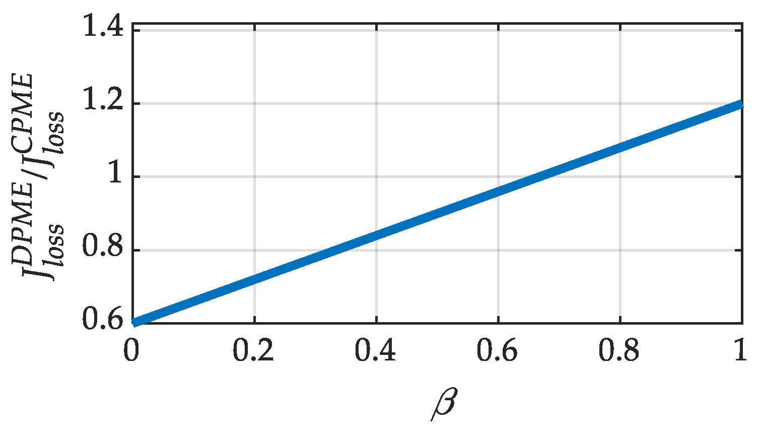
The same procedure was conducted to determine the percentage improvement in terms of power losses through calculating the metric
Jloss for the two control strategies. This comparison was performed considering the impact of the capacitor resistance
Rdc. The latter was related to the leg resistance
Rleg through the loss factor
β, which ranged from 0 to 1 with a step of 0.01, and was defined as
This is because the capacitor resistance is typically lower than the leg resistance. Indeed, the latter includes the equivalent series resistance of the arm inductors and the on-state resistance of the semiconductor devices employed. In this way, when calculating the ratios of the metrics Jloss for the two control strategies considering (31), the resistance Rleg terms are simplified. Therefore, this ratio also depends solely on the percentage of arm active power mismatches and resonant factor.
The results are depicted in
Figure 4, and it can be observed that the DPME control strategy experiences lower power losses for
β lower than 0.67. Ideally, the
Jloss could be reduced by about 40%.
The previous analysis was performed via assuming a uniform probability density function for the arm active power mismatches Pd,k. However, according to the system specifications and topology, a specific probability density function can be assumed, potentially leading to different results in the comparison. In conclusion, if the DC-side capacitor is properly designed, the DPME control strategy may yield significant improvements compared to the CPME control strategy in terms of required AC circulating voltages, their equalization, and lower power losses.
5. Simulation Results
In this section, simulation results are provided to demonstrate the proposed design procedure. The 20 kW MMC-PV system connected to a 400 V network of [
20] was considered. However, it should be noted that the arm resistance did not account for the conduction resistance of the semiconductor devices. To ensure a fair comparison between the two control strategies and validate the proposed sizing procedure, the arm resistance,
Rarm, needs to be increased to include the resistance of the semiconductor devices.
On the other hand, the switching characteristics of such devices are not relevant for this analysis. Therefore, we selected a MOSFET available in the market, specifically the IPB200N15N3 (40 A–150 V) by Infineon [
22], with a drain-to-source resistance of 20 mΩ. The main system parameters are reported in
Table 1.
The MOSFET was chosen based on the rated arm current, i.e., 29 A, determined through considering the rated power plant, as indicated in
Table 1. The SM voltage was evaluated at maximum irradiance, taking into account the open-circuit voltage of the PV arrays at the chosen minimum allowed temperature of 10 °C, according to the parameters listed in
Table 2. Moreover, also the AC circulating components should be considered in the design phase. For this reason, the MOSFET was selected, assuming a safety margin of 30% in rated voltage and current.
In addition, the
P-
V characteristic of the equivalent PV array embedded in the
i-th converter SM was modeled as following [
19]
where subscript
x is
up for the upper arm and
low for the lower arm,
Gx,i is the solar irradiation,
VPV,x,i is voltage of the
i-th PV array, and
nPV,series and
nPV,parallel are the series- and parallel-connected PV modules. The ambient temperature was fixed at 25 °C.
The DC-side capacitor was designed according to the procedure proposed in
Section 4.1, considering the sum of the optimal operating voltages of the arm PV arrays under maximum irradiance conditions as the rated DC-side voltage:
where
VPV,max represents the optimal operative voltage (i.e., 87.8 V) of the equivalent PV array at an irradiance value of 1000 W/m
2, and
N is the number of SMs per arm.
The optimal capacitance was determined through evaluating the cost function (29). In particular, the sizing procedure was conducted for two capacitors available in the market, and we selected the one that allowed us to achieve the lowest cost function. Moreover, since the capacity reactance is defined as a function of the leg reactance (i.e.,
Xdc = αXleg with
α ranging from 0 to 1), for the considered system, the minimum capacity reactance is equal to 1.26 Ω. Given the required voltage and capacity levels, only electrolytic capacitors are available. The TDK series B43700 aluminum electrolytic capacitors (600 V DC) [
23] and the KEMET ALS70/71 aluminum electrolytic capacitor (630 V DC) [
24] were considered. Therefore, to assess the influence of the equivalent series resistance of the capacitors, the relationship between tan
δ and
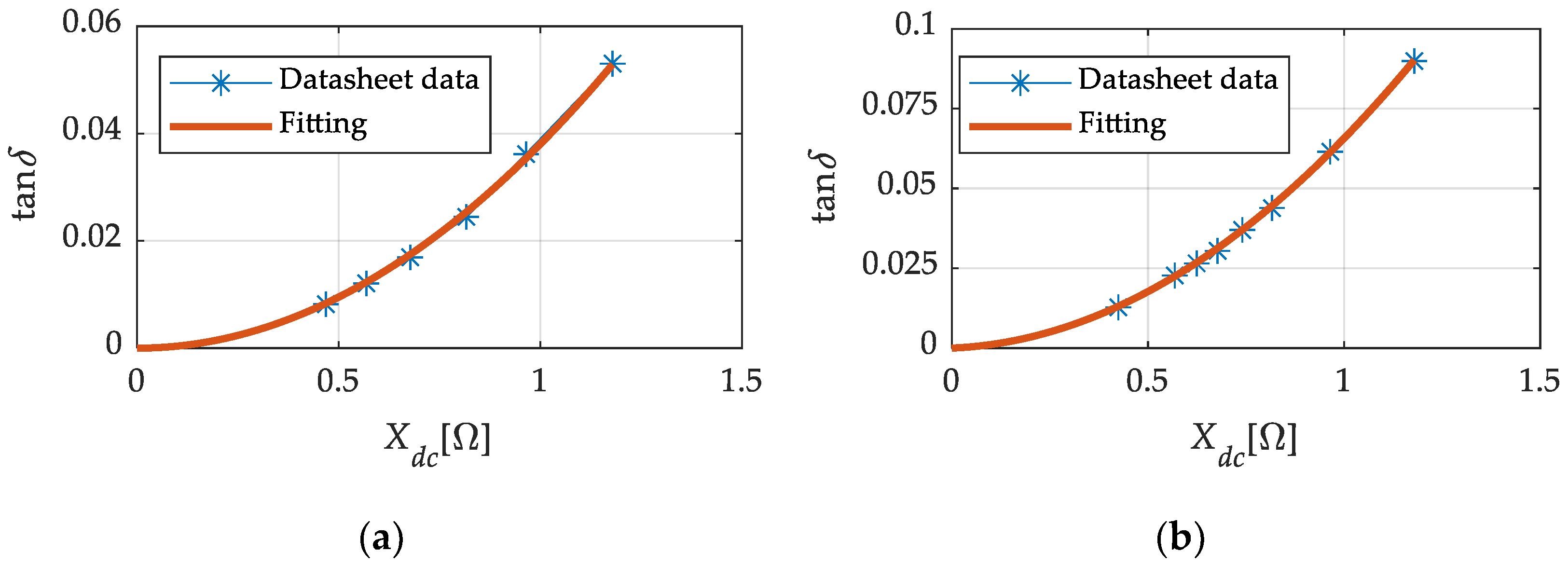
Xdc at 50 Hz was obtained through fitting the technical data from the datasheets (
Figure 5). In this case, a second-order polynomial function was used for the fitting, as follows:
As before, the design procedure was performed considering a uniform probability density function for the arm active power mismatches. Consequently, considering (34), (27), and (28), the cost function (29) can be expressed as a function of resonant factor α.
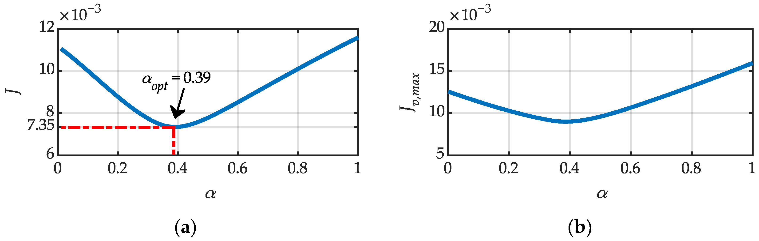
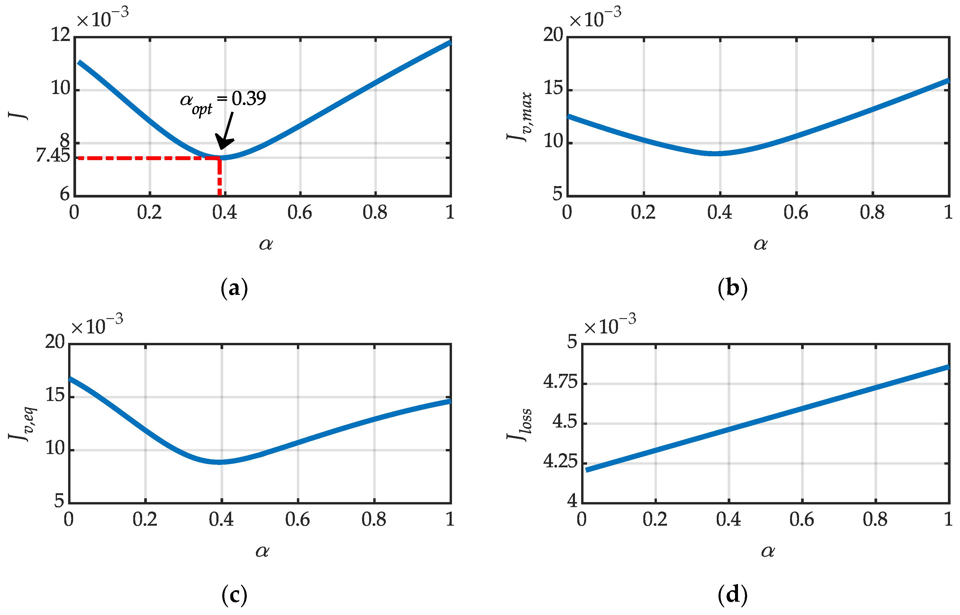
Figure 6 and
Figure 7 illustrate the three metrics and the cost function
J for α values ranging from 0 to 1 for the TDK series B43700 and KEMET ALS70/71 capacitors, respectively. Looking at the figures reporting the three metrics separately, it becomes possible to identify the optimal resonant factor associated with the prioritization of a singular goal within the proposed sizing procedure. The results of the sizing procedure are listed in
Table 3. The table shows that, for both capacitors, the optimal resonant factor for the metrics
Jv,max,
Jv,eq, and
Jloss are the same and equal to 0.39, 0.39, and 0.01, respectively. Naturally, since the metric
Jloss is linked to the power losses, the optimal solution is achieved with the minimum resonant factor, corresponding to the lowest resistance. The costs of the metrics
Jv,max and
Jv,eq are independent from the equivalent series resistance of the capacitor. They are influenced solely by the probability distribution of the arm active power mismatches and the leg reactance. For this reason, their costs are the same for both capacitors. However, the cost related to the power losses depends on the loss tangent characteristic of the capacitor. In this case, for the TDK series B43700, the cost associated with the metric
Jloss is lower than that of the KEMET ALS70/71 capacitor, making it more efficient.
Additionally, the cost function (29) for the two capacitors was evaluated considering equally weighted factors, i.e., wv,max = wv,eq = wloss = 1/3. Since the economic aspect of the analysis is out of the scope of this work, the same priority was given to the minimization and equalization of AC circulating voltages and the minimization of the overall power losses. On the other hand, through assigning different weights to the three defined metrics or considering various probability distributions of arm active power mismatches, different outcomes can be obtained.
In the considered case, through evaluating (30) for the two capacitors, the optimal value of the resonant factor,
αopt, was found to be 0.39, corresponding to a capacitance value of 6.5 mF and a cost function
J of 0.00735 and 0.00705 for the TDK and KEMET capacitors, respectively. However, the final choice should be made according to the available capacity values defined by the datasheets. In this regard, for the TDK series B43700 [
23], the closest value is 6.8 mF, determining the actual resonant factor
α to be 0.37 and the cost function
J to be 0.00737. On the other hand, for the KEMET ALS70/71 [
24], two possible sizes are available, which are 5.6 mF and 7.5 mF. The former resulted in a resonant factor
α and cost function
J equal to 0.45 and 0.00761, respectively, while the latter resulted in a resonant factor
α and cost function
J equal to 0.34 and 0.00756, respectively. Thus, between the two capacitors, the final choice fell on the TDK series B43700. Two capacitors were connected in series to achieve the required DC-side voltage and ensure a certain margin in case of voltage fluctuations. On the other hand, the capacitance was halved to 3.4 mF. To reach the optimal capacitance value, two more series-connected capacitors were connected in parallel. This resulted in an equivalent capacitance of 6.8 mF and an equivalent series resistance of 17.5 mΩ. According to the computed equivalent series resistance, the factor
β is equal to 0.07. Through adopting this solution, the DPME control strategy demonstrated improvements of 36%, 25%, and 36% for the metrics
Jv,max,
Jv,eq, and
Jloss, respectively, compared to the CPME control strategy.
In the following, the numerical results of the operation of the MMC-PV system for the two control strategies are provided. Since the analysis is focused on the AC circulating currents, non-homogeneous irradiance conditions among the converter arms were analyzed. The analyzed scenarios were defined to highlight the main differences between the two control strategies in cases of large power mismatches.
5.1. Partial Shading Conditions between the Arms of One Leg
In this scenario, partial shading conditions between the arms of one leg were analyzed. This situation causes the AC circulating currents to flow through the converter, leading each arm to operate at its maximum power point. The generated arm powers and their corresponding irradiance values are reported in
Table 4.
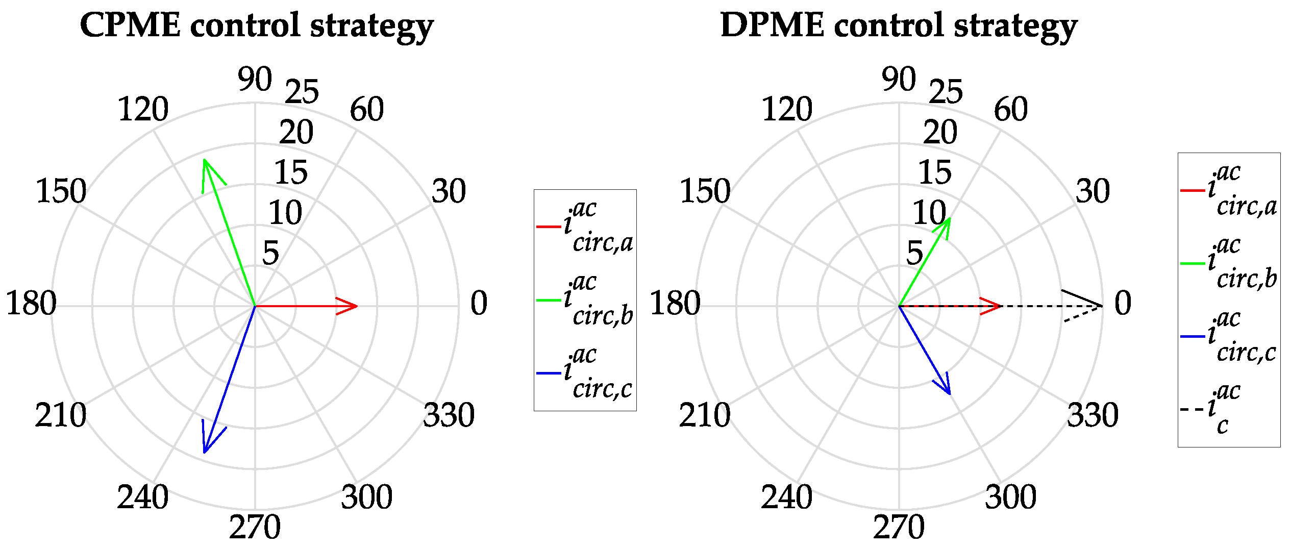
In the MMC topology that includes the DC-side capacitor (DPME control strategy), the AC circulating current only flows through the unbalanced phase (leg
a) and recloses through the DC-side capacitor without involving the other two converter legs. On the other hand, in the MMC topology without the DC-side capacitor (CPME control strategy), the AC circulating current must reclose through the other converter legs, leading to reactive power exchange among the arms. The AC circulating currents generated by the DPME and CPME control strategies were evaluated through (18) and (23), respectively.
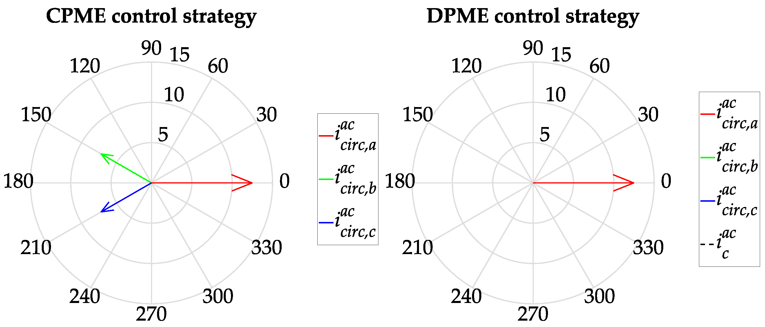
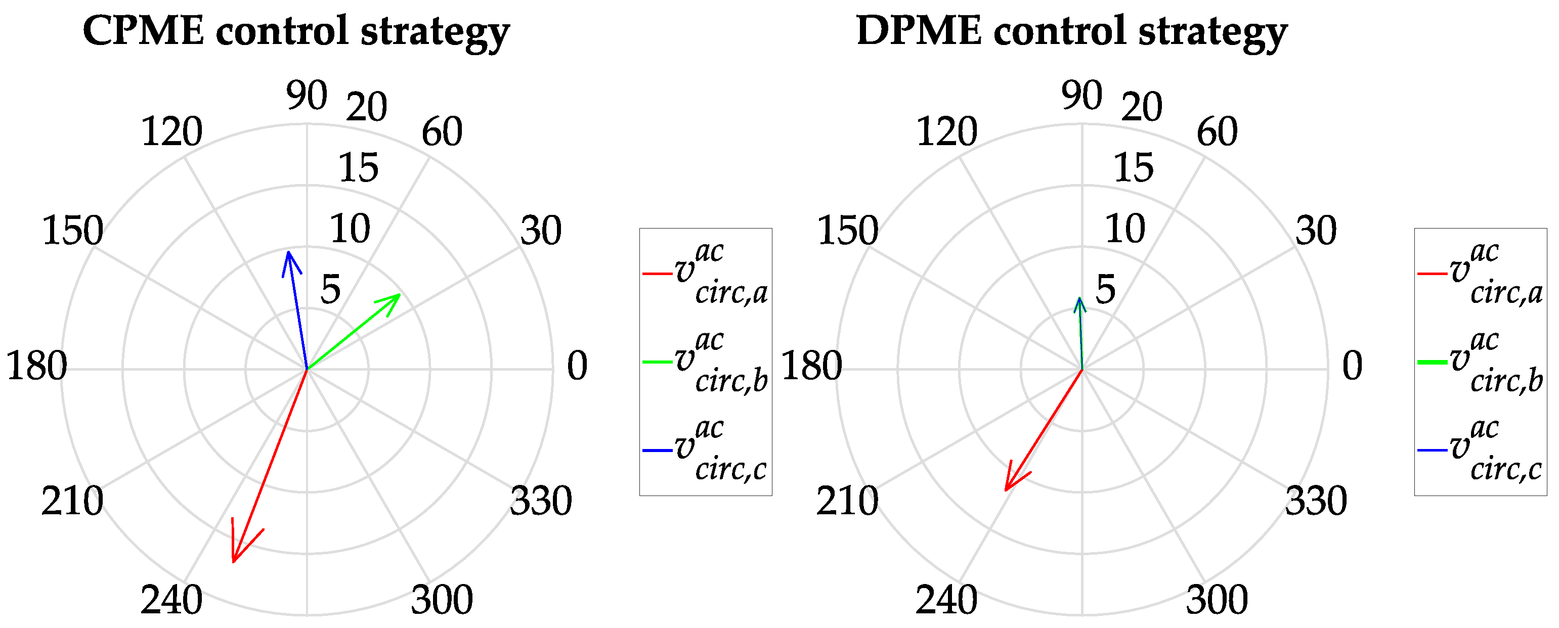
Figure 8 shows the phasors referred to the output phase grid voltage component
vph,k. From this figure, it is possible to note that, through adopting the DPME control strategy, only the AC circulating current of the unbalanced phase (leg
a) is required, which corresponds to the AC capacitor current. Instead, with the CPME control algorithm, the AC circulating current components of phase
b and
c are also generated. The latter result to be 90° out of phase with the corresponding output phase voltage components indicating the exchange of reactive power. Moreover, these additional circulating currents result in increased power losses. Specifically, when evaluating the
Jloss metric for this specific irradiance condition, the power losses for the CPME algorithm were found to be 61% higher than those of DPME. In particular, they amounted to 1.02% and 0.63% of the exchanged power (12.2 kW) for the CPME and DPME control strategies, respectively.
The AC circulating voltages were evaluated through (19) and (24), and the corresponding phasors are presented in
Figure 9. In the case of the CPME algorithm, the circulating voltages are consistently about 90° out of phase with the corresponding circulating currents, indicating predominantly inductive internal converter impedance. On the other hand, in the case of the DPME strategy, the circulating voltages also depend on the voltage drop across the DC-side capacitor. According to the proposed sizing procedure, it aims to minimize and equalize the necessary AC circulating voltages of the three converter phases. In particular, when separately evaluating the metrics
Jv,max and
Jv,dev for this specific irradiance condition, it was found that the circulating voltages of the CPME algorithm were 44% higher than those of the DPME algorithm, and their deviation for the CPME algorithm were 22% higher than those of the DPME algorithm. In particular, the maximum circulating voltage was 1.6% and 1.1% of the rated DC-side voltage (1053.6 V), for the CPME and DPME control strategies, respectively. The maximum deviation among the three voltages was 1.3% and 1.1% of the rated DC-side voltage for the CPME and DPME control strategies, respectively. Lastly, the cost function (29) evaluated for the CPME and DPME control strategies yielded values of 4.0 and 2.8, respectively, demonstrating that through adopting the DPME control strategy along with an optimal DC-side capacitor, the overall converter performances can be improved.
5.2. Partial Shading Conditions between Arms of Three Legs
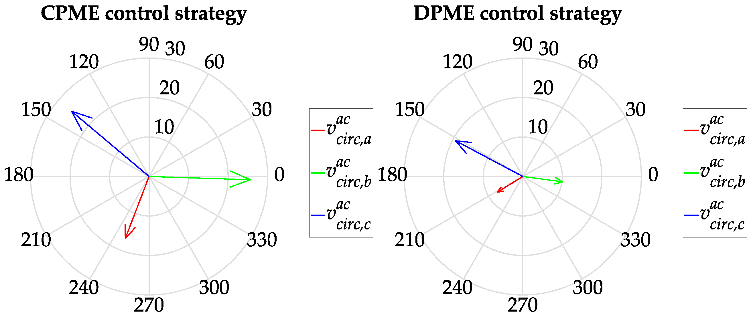
In this scenario, partial shading conditions between the arms of the three converter legs were analyzed. In this case, the arm irradiance values were set to analyze significant arm power mismatches. The resulting arm powers and the corresponding irradiance values are reported in
Table 5.
In this situation, exchanging power among all the converter arms is necessary to optimize the converter operation. The phasors of the AC circulating current components referred to the output phase grid voltages
vph,k are shown in
Figure 10. Looking at the results, it is evident that, with the DPME algorithm, the AC circulating current phasors are always aligned with the related output phase grid voltage generated by the arm. In particular, they can be in phase or opposite phase based on the direction of the arm power mismatch. In addition, the sum of the AC circulating currents flows through the DC-side capacitor. Instead, with the CPME control strategy, a phase displacement is necessary since the sum of AC circulating currents must be zero. Therefore, the amplitude of these phasors is higher since reactive components are needed. Through separately evaluating the metric
Jloss for this specific irradiance condition, it was found that the power losses of the CPME algorithm were 80% higher than those of the DPME algorithm. In particular, they were 3.46% and 1.92% of the exchanged power (12.2 kW) for the CPME and DPME control strategies, respectively.
The phasors of the AC circulating voltages generated by the DPME and CPME strategies are reported in
Figure 11. Also in this case, for the CPME algorithm, the AC circulating voltages are about 90° out of phase with respect to the corresponding circulating currents, while in the case of the DPME strategy, they depend on the voltage drop on the DC-side capacitor and, therefore, on the sum of the AC circulating currents.
Through separately evaluating the metrics Jv,max and Jv,eq considering this specific irradiance condition, it was found that the circulating voltages of the CPME algorithm were 33% higher than those of the DPME algorithm, and their deviation for the CPME algorithm was 23% lower than those of the DPME algorithm. In particular, the maximum circulating voltage was 2.4% and 1.8% of the rated DC-side voltage (1053.6 V) for the CPME and DPME control strategies, respectively. The maximum deviation among the three voltages was 1.7% and 2.2% of the rated DC-side voltage for the CPME and DPME control strategies, respectively. Lastly, the cost function (29) evaluated for the CPME and DPME control strategies yielded values of 7.6 and 6.0, respectively, demonstrating that through adopting the DPME control strategy along with an optimal DC-side capacitor, the overall converter performances can be improved. Of course, different weight factors of the cost function (29) can be selected, resulting in different optimal values of the DC-side capacitor. These optimal values can have different impacts on the defined metrics.
6. Conclusions
This paper proposed a sizing procedure for the DC-side capacitor of an MMC-based PV three-phase system controlled using the DPME algorithm. Moreover, a comparison was performed with respect to the MMC topology without the DC-side capacitor controlled with the CPME algorithm. In scenarios in which power mismatches due to partial shading occur among the converter arms pertaining to same converter leg, managing the AC circulating currents is crucial for optimizing system performance. The circulating currents must be generated to make the arms work at their optimal power point, always injecting the maximum power into the grid. In the case of an MMC without the DC-side capacitor, depending on the arm power mismatches, an additional reactive power exchange can be requested due to the coupling of the phases, resulting in higher circulating voltages, worse equalization of them, and higher power losses. On the other hand, in the presence of the DC-side capacitor, the three converter phases can be decoupled from each other. Thus, the AC circulating currents can flow only on the unbalanced phases, and their sum will reclose in the DC-side capacitor. Through properly sizing the latter, overall power losses can be reduced, and the circulating voltages can be minimized and equalized.
The proposed sizing procedure was based on an in-depth theoretical study performed to evaluate the internal MMC power flow, considering the equivalent electric circuit for the AC circulating components. Through this analysis and through minimizing the proposed cost function (29), the optimal design of the DC-side capacitor could be determined. The cost function (29) comprises three metrics related to the minimization and equalization of the AC circulating voltages, as well as the minimization of the power losses. The sizing procedure was conducted through expressing the capacitance reactance Xdc as a function of the leg reactance Xleg through the resonant factor α. Moreover, the equivalent series resistance of the capacitor, Rdc, was correlated to its reactance, allowing the three metrics of the cost function (29) to be expressed in terms of α. Finally, through selecting a probability density function related to possible partial shading conditions, the optimal capacitance value could be determined.
The simulation results confirmed that, according to the proposed sizing procedure, the DPME control strategy can be more effective compared to the CPME control strategy in terms of the maximum AC circulating voltages required to drive the related circulating currents, the equalization of those voltages, and the minimization of power losses. In fact, the DC-side capacitor can reduce internal converter impedance, thereby requiring lower circulating voltages and improving their equalization. On the other hand, the overall converter efficiency depends on the equivalent series capacitor and leg resistances. Since the equivalent series capacitor resistance is typically much lower than the leg resistance, which includes the resistance of the inductors and semiconductor devices, the MMC with the DC-side capacitor results in lower power losses.


