Article

Effect of Interfacial Oxide Layers on Self-Doped PEDOT/Si Hybrid Solar Cells

1
Institute of Fluid Science, Tohoku University, Sendai 980-8577, Japan
2
National Institute of Advanced Industrial Science and Technology, Tsukuba 305-8568, Japan
3
Institute for Materials Research, Tohoku University, Sendai 980-8577, Japan
4
Organic Materials Research Laboratory, Tosoh Corporation, Shunan 746-8501, Japan
5
Graduate Faculty of Interdisciplinary Research, University of Yamanashi, Kofu 400-8510, Japan
6
Institute of Communications Engineering, National Yang Ming Chiao Tung University, Hshinchu 30093, Taiwan
*
Author to whom correspondence should be addressed.
Energies 2023, 16(19), 6900; https://doi.org/10.3390/en16196900
Submission received: 5 September 2023 / Revised: 24 September 2023 / Accepted: 28 September 2023 / Published: 30 September 2023
(This article belongs to the Special Issue Emerging Technologies for Multijunction Solar Cells)

Abstract

:
PEDOT:PSS/Si hybrid photovoltaic cells have been attracting attention as a potential way to simplify the manufacturing process and democratize solar energy production. Control of the PEDOT/Si interface is also one of the primary ways to ensure the improved performance and lifetimes of multijunction devices, such as perovskite/Si tandem solar cells. In this work, the effects of the interfacial silicon oxide layer were investigated by creating a novel and controllable neutral beam oxide interlayer with different thicknesses. A novel self-doped PEDOT (S-PEDOT) was used to improve interfacial contact and avoid the secondary doping of PEDOT:PSS. X-ray photoelectron spectroscopy (XPS) showed that the saturation of interfacial silicon atoms in SiOx-Si bonds as well as a very thin, (~1 nm) damage-free oxide interlayer were the keys to maintaining good passivation with a high tunneling current. Lifetime measurements also showed that the interlayers with the most SiO2 content degraded the least. The degradation of the devices was due to the continued growth of the oxide layer through reactions with silicon sub-oxides and the degradation of S-PEDOT.

1. Introduction

Research on inexpensive, renewable energy devices has become a generational challenge of our time due to the alarming rate and effects of global warming [1]. Despite falling prices, the cost of the PV module still accounts for the largest percentage of investments in solar cells [2,3]. This is in part due to high-temperature (≥850 °C) dopant diffusion and annealing processes that are usually required in the manufacturing of silicon homojunction photovoltaic cells, which dominate the market. These processes are naturally complex and time consuming, which contribute to the high unit cost. Recently, so-called third generation solar devices have increasingly started to move towards silicon heterojunction solar cells that use relatively lower temperature (~200 °C) processes. Si heterojunction solar cells using hole-selective TiO2 layers, for example, have been able to reach efficiencies of 21% [4]. In the field of organic hole-conducting materials, poly (3,4-ethylenedioxythiophene):poly styrenesulfonate (PEDOT:PSS) has similarly gained a lot of interest. Whether it be used for new flexible or rigid perovskite cells [5,6,7] or in tandem and multijunction cells [8,9,10], PEDOT:PSS has multiple uses ranging from a transparent hole transport layer (HTL), or an efficient interconnection between subcells to a thin conductive bonding layer for lattice-mismatched materials. Silicon–organic hybrid solar cells (SOHCs) can also exploit the low-cost processing techniques of such conjugated polymers and the optoelectrical properties of Si to reduce the module cost while maintaining high performance. As light absorption and photocarrier generation primarily occur in the Si substrate, these devices can theoretically achieve comparable efficiencies to that of conventional homojunction cells. PEDOT:PSS is a conductive polymer material consisting of a conjugated positively charged PEDOT and negatively charged PSS. PEDOT usually acts as a highly conductive, transparent HTL, while the polymer, PSS, improves the dispersion and stability of PEDOT in solvents, such as water. Architectures that use n-type Si as the absorber and PEDOT:PSS as the front transparent carrier-selective contact have been able to achieve device efficiencies exceeding 17% to date [11]. With further optimization, these solar cells can potentially reach 20% efficiencies, making them a competitive, low-cost alternative to organic or perovskite PV cells.
Despite their initial success, PEDOT:PSS SOHCs face some challenges that prevent them from being rapidly adopted for commercial applications. (i) PEDOT:PSS exists in the form of a colloidal dispersion as hydrophobic PEDOT that is surrounded by an excess of hydrophilic PSS. The gel-like structure of the colloidal particles (12–50 nm in diameter) hampers the overall conformity of the deposited layer around nanostructures that are typically used for improving light trapping and the interfacial junction area in these types of cells. We demonstrated this property in Figure 1a, where PEDOT:PSS was spin coated on top of silicon nanocones etched using a combination of a self-assembled ferritin template over an SiO2 mask layer followed by subsequent etching using NF3 and Cl2 neutral beams [12]. (ii) Pristine PEDOT:PSS exhibits poor electrical conductivity (<1 S cm−1) [13], making it necessary to use additives, such as ethylene glycol (EG), dimethyl sulphoxide (DMSO), or sorbitol, to improve the conductivity with varying degrees of success [13,14,15,16,17,18,19]. This step complicates the overall production process. (iii) PEDOT:PSS has an oxidizing effect on silicon substrates and promotes the growth of a silicon oxide (SiOx) layer [20]. Such an interfacial oxide layer acts as a potential barrier in the J–V curve of the cell, resulting in an anomalous behavior often characterized as an “S-shape” [21,22]. The first two factors can be attributed purely due to the presence of PSS in the final thin film. Therefore, the realization of a fully soluble self-doped PEDOT (S-PEDOT) has been intensely researched, and a highly conductive (>1000 S cm−1) version of the same was finally realized [23]. S-PEDOT has the advantage of being highly conformal to substrate nanotexturing (Figure 1b) with fewer voids caused by PEDOT: PSS particles. This mitigates the first two pain points in SOHC production. The third factor may be caused by a combination of ineffective passivation and degradation of PEDOT [24,25]. While the formation of the SiOx-Si bond is beneficial as it produces a net positive surface dipole, inducing good band orientation compared to H-Si bonds in pristine silicon, the thermally grown thin oxide layer (<1 nm) grows to approximately 2 nm thick within a week underneath a PEDOT:PSS film [22]. This interfacial oxide layer has been popularly grown either by leaving pristine silicon samples overnight to oxidize naturally [21] or by dipping in an oxidizing aqueous solution [26]. However, while the former method produces a larger variance in the quality of the oxide layer across the wafer, the layer using the later method is very difficult to control to within 1 nm, which is usually the target thickness. Table 1 provides a summary of solar cell structures and parameters for similar planar PEDOT/Si SOHCs with a SiOx layer at the interface as reported previously. Although Trujillo et al. [22] have also characterized a similar device structure with a siloxane passivation layer, their work did not provide explicit PV parameters and focused on the deterioration of cell characteristics over time. The comparisons to our findings will be discussed later.
This work aims to study the effect of controllable approximately nanometer thin oxide passivating layers on the performance and lifetime of hybrid solar cells. As shown in Table 1, planar SOHCs were fabricated using a novel, highly conductive S-PEDOT as the top transparent hole-transporting layer (HTL) over an n-type Si substrate passivated by an interfacial oxide layer (Figure 2). We chose to use the roughly etched, non-polished Si surface for preliminary experiments instead of nanotextures in order to better study the oxide layer. A 1 nm-thick oxide layer made using the neutral beam oxidation (NBO) method was able to achieve a more homogenous and defect-free layer, producing more repeatable results compared to thermal oxidation. The maximum efficiency achieved was 6.35% for a cell with thermally grown oxide (TO). However, the variance of samples cut from the same wafer was much larger compared to those using a neutral beam oxide (NO) layer. The average efficiencies of both samples were approximately the same at 5.59% and 5.53% for TO and NO samples, respectively.

2. Materials and Methods

2.1. Sample Preparation

In this study, 2″ n-type CZ silicon (100) wafers with 1–5 Ω·cm resistivity were used. The thickness of the wafer was 380 ± 20 µm. One side of the wafer was a polished mirrored surface, and the other side was an etched rough surface. An n+-Si back surface field (BSF) was grown on the mirrored surface with a custom-built solid-source molecular beam epitaxy (MBE) using a system equipped with an electron gun to form a Si molecular beam [29]. First, n-type Si (001) wafers were cleaned using a standard RCA procedure. After thermal cleaning was performed at 700 °C for 10 min to remove all surface oxides, a 150 nm-thick n+-Si BSF layer doped with phosphorous was grown at a growth rate of 1.2 Å/s at 600 °C to achieve a carrier concentration of 5.0 × 1018 cm−3. The wafers were then cut into 18 × 18 mm square. An Au-Sb/Au rear side contact was deposited onto the n+-Si BSF surface using an electron beam evaporator. Then, metallization was performed at 400 °C for 20 min under an ambient nitrogen environment. The samples were then cleaned using piranha solution at a 2:1 ratio of H2O2:H2SO4 for 3 min, and the native silicon oxide layer was etched away using 0.5% HF solution for 2 min. Two types of interfacial oxide layers were grown on the non-polished rough surface of these pristine Si samples. A highly thin 0.7 nm-thick native oxide layer was grown by placing the samples on a hotplate at 150 °C for 15 min under air ambient conditions. The second type of oxide layer was grown using oxygen plasma at 500 W bias for 400 s passed through a high-aspect ratio carbon aperture onto the substrate at 400 °C. The aperture blocks all high-energy UV radiation and neutralizes all charged species in the plasma, leaving only neutral oxygen radicals, which are absorbed by the silicon surface in a damage-free process called neutral beam oxidation (NBO) [2]. The thickness of the SiOx layer obtained using this procedure was typically 4.62 nm. Then, the SiOx layer was etched down to thin tunneling layers using 0.5% HF solution for different durations at room temperature. S-PEDOT (supplied by Tosoh Corporation) was then spin coated at 1100 rpm for 60 s and at 3000 rpm for 5 s, resulting in a thickness of 180 ± 10 nm. The thickness of the S-PEDOT layer was measured using a Kosaka Laboratory Surfcorder ET200A in a separate experiment (not shown here). PEDOT: PSS (Clevios PH1000 made by Heraeus in Leverkusen, Germany) with 3% wt. EG was spin coated at 1500 rpm for 60 s and at 3000 rpm for 5 s to obtain a coating with a similar thickness on other separate substrates to serve as a control. The PEDOT coatings were dried at 60 °C for 30 min and annealed at 130 °C for 15 min under air ambient conditions. After the deposition of the PEDOT emitter, 500 nm thick Ag finger grids were evaporated on the front side (~500 nm thick layer). A 100 nm thick MgF2 protective coating was finally deposited on the front surface using a thermal evaporator. Finally, each individual 18 × 18 mm sample was cut into 4 separate 6 × 6 mm solar cells.

2.2. Characterization

The solar cells were characterized by measuring the external quantum efficiency (EQE) using chopped monochromatic light with a constant photon flux of 1 × 1014 cm−2. The current density–voltage (J–V) characteristics were measured under airmass 1.5 global (AM1.5G) illumination at 100 mW/cm2. We used an aperture area of 0.29 cm2 for the EQE and J–V measurements by subtracting the shadow area associated with the finger grids. The reflectance properties of S-PEDOT from 200 to 1200 nm were measured using a UV-vis-NIR spectrophotometer model ARSN-733 by JASCO Corporation. The composition and thickness of the interfacial oxide layer was characterized using X-ray photo spectroscopy (ULVACPHI ESCA1600 by ULVAC in Chigasaki, Japan) with a monochromatic Al Kα source.

3. Results

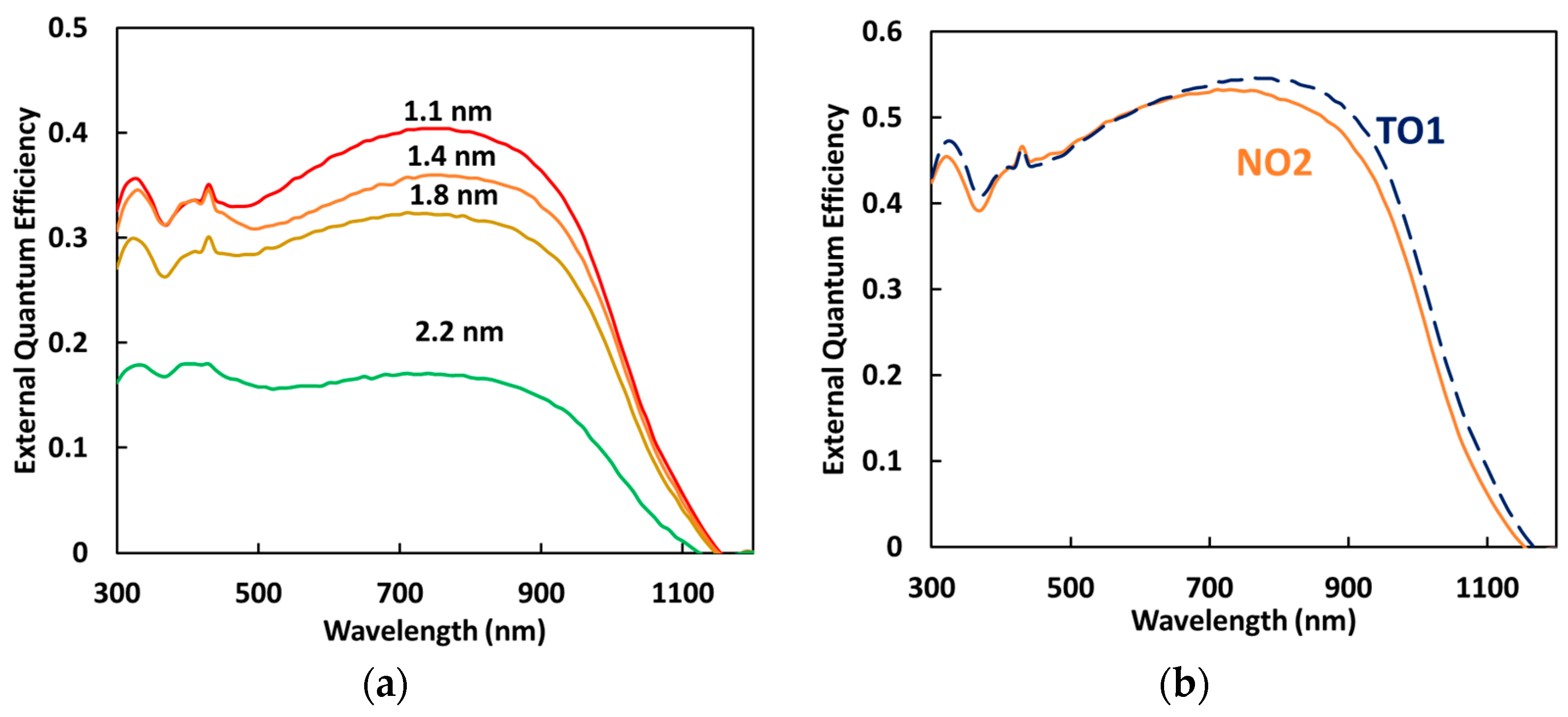
3.1. Optical Properties

The UV-vis-NIR absorbance spectra of S-PEDOT were measured on quartz substrates and compared to PEDOT:PSS (Clevios PH1000 by Heraeus) secondary doped with 3% EG, which is typically used in Si/PEDOT:PSS SOHCs. Figure 3 shows the normalized absorbance spectra of the measured samples. The overall absorption of the S-PEDOT thin film after 237 nm is higher than PEDOT:PSS. This is associated with a higher optical density of PEDOT in the former compared to an excess of PSS in PEDOT:PSS film. The absorption peak at 226 nm can be assigned to the aromatic rings in PSS, which are clearly not present in S-PEDOT (Figure 3). While S-PEDOT also has strong absorption in the 200–300 nm region, it does not display any sharp peaks due to the absence of the PSS chains characteristic of PEDOT:PSS.

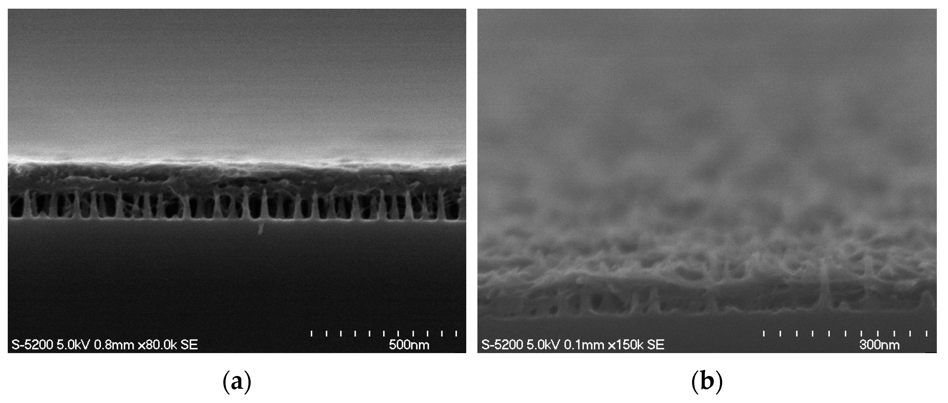
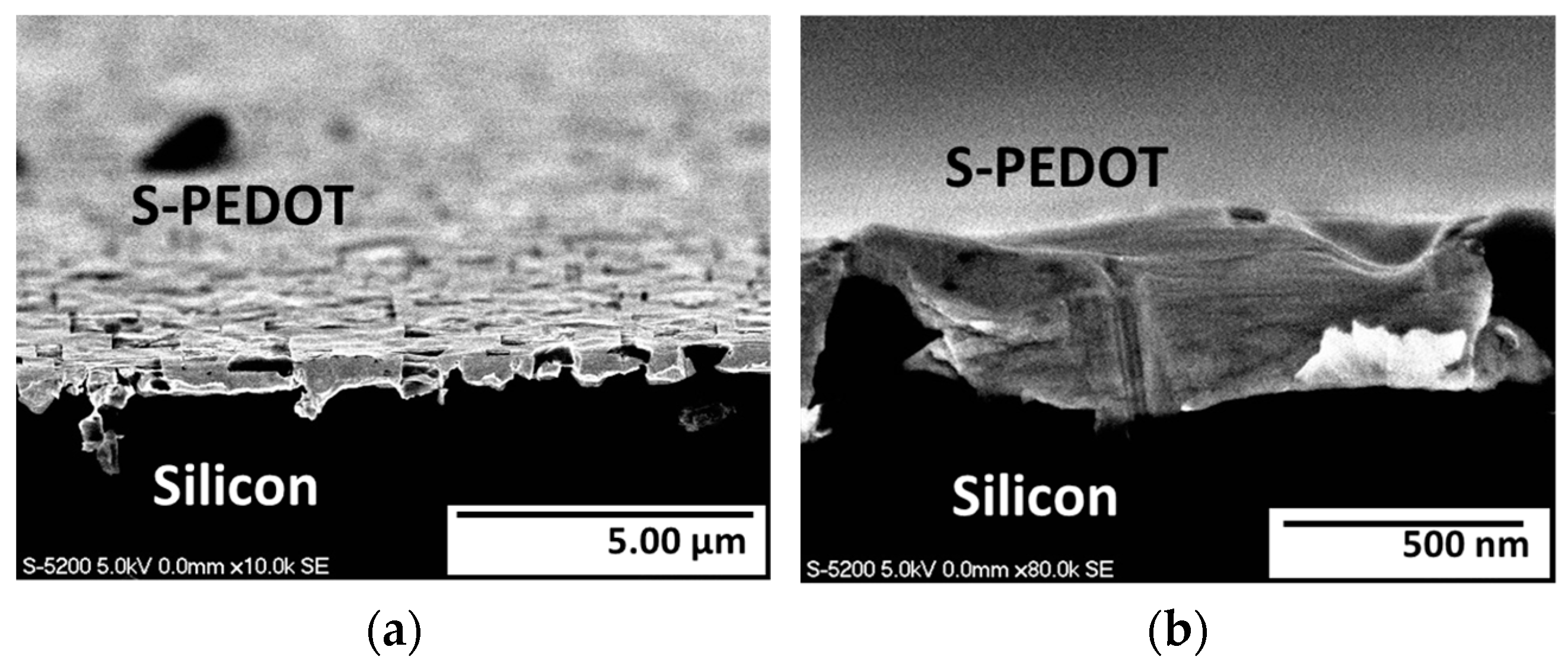
3.2. Surface Morphology

The morphology of S-PEDOT on the rough Si surface was observed using atomic force microscopy (AFM) and a scanning electron microscope (SEM). The non-polished rough surface comprises grooves and crevasses between 1 and 3 μm in width and approximately 200 and 300 nm in depth. As seen in Figure 4a,b, the coated S-PEDOT film penetrated to the bottom of all the undulations, improving the contacting area to the Si rough surface. This resulted in a flatter surface (Rrms = 0.94 nm) compared to PEDOT:PSS when coated over the same surface (Rrms = 4.73 nm) under the same conditions.

3.3. Characterization of Interfacial Oxides

As mentioned above, two types of interfacial oxides were grown for the SOHC samples, the thermally grown (TO) and the neutral beam (NO) layer samples. The later were etched down to the desired thickness using 0.5% HF solution at room temperature. The etching rate of SiO2 by HF is a complicated process and depends on mainly (i) the saturation of the oxide layer (i.e., the presence of sub-oxides), (ii) the pH of the solution, and (iii) the concentration of HF [30]. However, factors, such as thin SiO2 layers and the illumination of n-Si, tend to hinder the etching process [31]. XPS was used to determine the thickness of the silicon oxide layer. This method allows for a more accurate calculation of thickness compared with ellipsometry measurements as they are not affected by any contamination layer on the substrate. Additionally, XPS allows for the quantification of the relative amounts of the different valence states of silicon present (Figure 5). All peaks were fit to the same Gaussian–Lorentzian convolution function with Shirley background subtraction. The silicon oxide peaks were referenced to the C1s peak in order to account for possible charging across the oxide [32]. The shape of the Si0 peak was estimated from an HF-etched substrate. The chemical shifts assumed for the Si4+, Si3+, Si2+, and Si1+ peaks with respect to the Si0 peak were 3.95, 2.55, 1.85, and 0.95, respectively. The thickness of the oxide layer was quantified from the Si 2p spectra using the relationship:
d = λ S i , S i O 2 × sin ( θ ) × l n I S i 4 + + I S i 3 + + I S i 2 + + I S i 1 + I S i 0 R + 1
where Ix is the measured intensity of the species x. λ Si , Si O 2 is the attenuation length of photoelectrons generated in the Si substrate through the oxide layer (3.3 nm). θ is the collection angle of the detector. R is given as follows:
R = ρ S i O 2 F S i λ S i , S i O 2 ρ S i F S i O λ S i , S i
where ρ x is the density of x, which is 2.33 g/cm3 and 2.27 g/cm3 for Si and SiO2, respectively, [33] and F x is the formula weight of x, which is 28 and 60 for Si and SiO2, respectively. λ S i , S i is the attenuation length of Si in Si (2.3 nm). The results of the oxide thickness of the measured specimens are shown in Table 2. The oxygen saturation of the oxide layer was estimated from the relative amounts sub-oxide intensities compared to saturated SiO2 using the following relation:
S a t u r a t i o n = I S i 4 + + 0.75 I S i 3 + + 0.5 I S i 2 + + 0.25 I S i 1 + I S i 4 + × 100
The NBO process is able to produce a highly saturated oxide layer (Figure 5) by bombarding the substrate with neutral oxygen radicals (<10 eV) that react with silicon as they penetrate and diffuse through the surface. This hyperthermal oxidation of silicon results in a top SiO2 layer and a layer of sub-oxides (SiOx) at the Si/SiO2 interface [34]. The sub-oxides comprise Si1+, Si2+, and Si3+ components in interfacial silicon atoms, which bind to one, two, or three nearest neighboring oxygen atoms, forming Si2O, SiO, and Si2O3, respectively. Exposure to the oxygen neutral beam for 400 s results in a 4.62 nm-thick oxide layer with an approximately 0.5 nm-thick sub-oxide interlayer. HF helped etch away excess SiO2 to achieve thin films that could allow charge carriers to tunnel through. However, prolonged etching times (>30 s) may have also promoted the reduction of Si ions to lower valence states, thus forming more sub-oxide species (Figure 5). After etching for 45 s, all the top SiO2 was etched away, resulting in an oxide film predominantly composed of Si2O and Si2O3 sub-oxides. This would also result in the formation of Si-H bonds on the exposed Si atoms on the surface.

3.4. Solar Cell Characteristics

The current density (J) vs. voltage (V) plots of the best performing cells are illustrated in Figure 6. As can be seen, there was a characteristic difference between the PEDOT:PSS control sample cells and those coated with S-PEDOT. The higher short-circuit current density (JSC) of the control sample may be a product of the higher conductivities of PEDOT:PSS compared to S-PEDOT. Although we were not able to confirm this independently, a recent study has published evidence of this [35]. The difference in the open-circuit voltage (VOC) between the two types of PEDOT, on the other hand, may be attributed to the improved coverage of S-PEDOT at the non-polished surface, resulting in better charge separation as mentioned in the previous section. Finally, the improved fill factor (FF) of the S-PEDOT cells can also be a result of fewer traps created by voids at the interface, although the FF deteriorated over time as shown below.
The champion TO cell had the best PV characteristics overall, achieving JSC = 21.99 mA/cm2, VOC = 480 mV, and FF = 60%, yielding a power conversion efficiency (PCE) of 6.35% (Table 3). However, it should also be noted that TO samples also showed the largest range in performance by having both the best and worst measured cells. All the NO samples had far more consistent characteristics, and, most notably, the efficiency of NO2 samples ranged from 5.49 to 5.69%. Measuring the thickness of the interfacial oxide layers for each type of sample would involve stripping the top layers either physically or chemically, thus risking damage to the layer itself. Therefore, the thicknesses of these layers were roughly estimated from the measurements shown above. The NO3 samples with the thinnest interfacial layer seemed to perform the worst and also showed a very slight “S-curve” shape, which is usually associated with degradation of the SOHC [22,36,37]. This behavior will be discussed later. The NO2 cells consistently measured better than the other two types of NO samples in all parameters. As shown in Figure 5, the thickness and component ratios of sub-oxides in TO1 and NO2 layers are very similar. The TO1 and NO2 samples also showed similar average PCE and fill factor readings (Table 3), possibly pointing to an optimum interfacial layer thickness between the 1.03 and 1.07 nm range. The thicker NO1 oxide layer samples seemed to result in a reduction in JSC, possibly because of reduced tunneling current through the interface.
EQE measurements of samples with different NO interlayer thicknesses ranging between 2.2 and 1.1 nm showed the effect of improved tunneling currents with thinner layers (Figure 7a). The narrow peak around 330 nm and subsequent dip at 370 nm can largely be attributed to the combined reflectance property of the PEDOT and MgF2 layers over the silicon substrate [38]. A large increase in EQE is observed when reducing the interlayer from 2.2 nm to 1.8 nm. This may be due to both fewer bulk carrier recombinations in the amorphous SiOx layer and improved tunneling properties. The broader peak between 550 and 1000 nm continues to improve even past 1.4 nm of the interlayer when the EQE at lower wavelengths remains mostly the same. Comparing the EQE of samples with different types of SiOx interlayers was more challenging as the thermal oxide layer is harder to control for such low thicknesses. Figure 7b compares EQE spectra between the cell with TO1 and NO2. The EQE response for the TO1 cell was slightly higher than NO2 samples. We will discuss the possible reasons for this difference later.

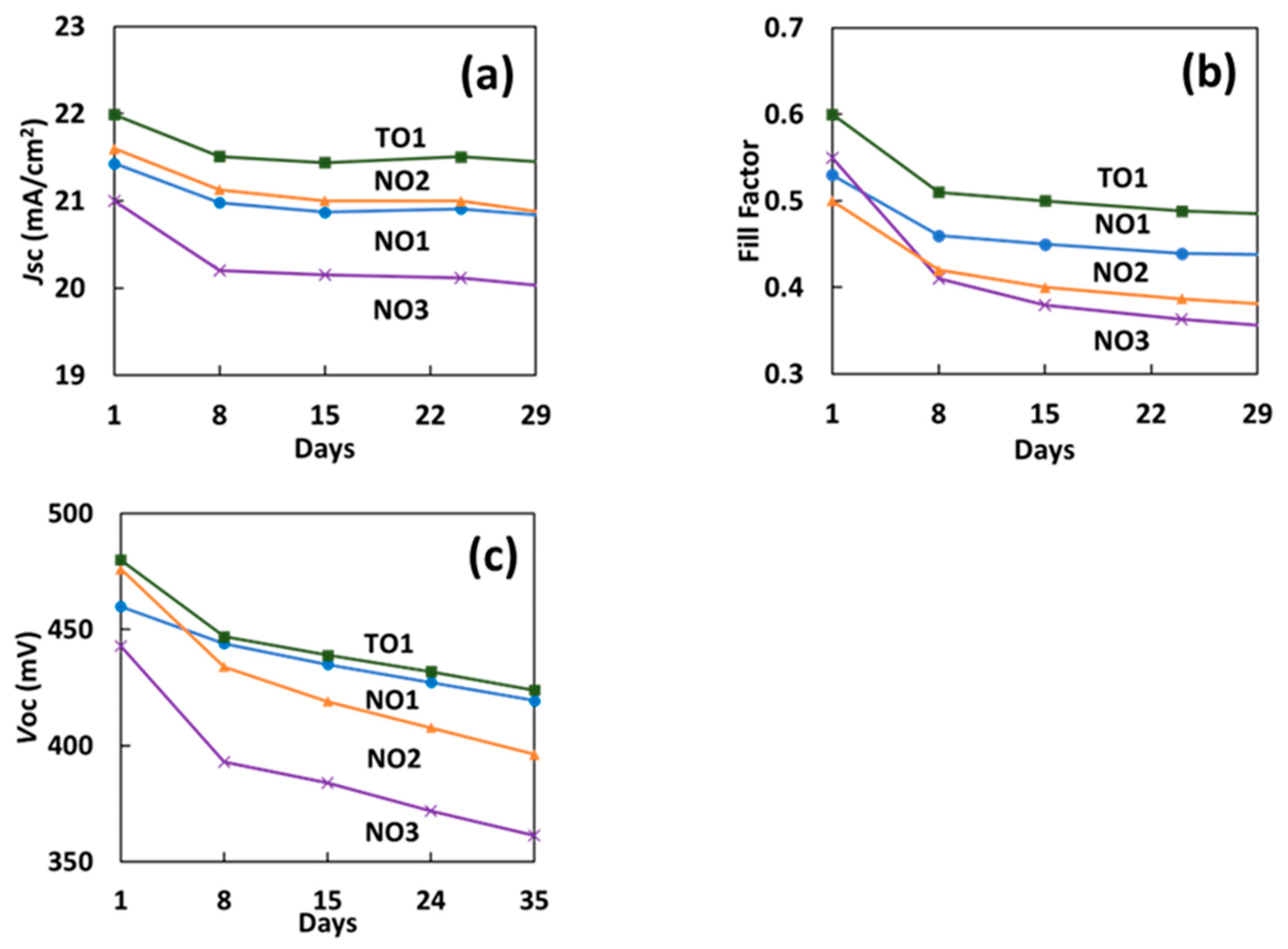
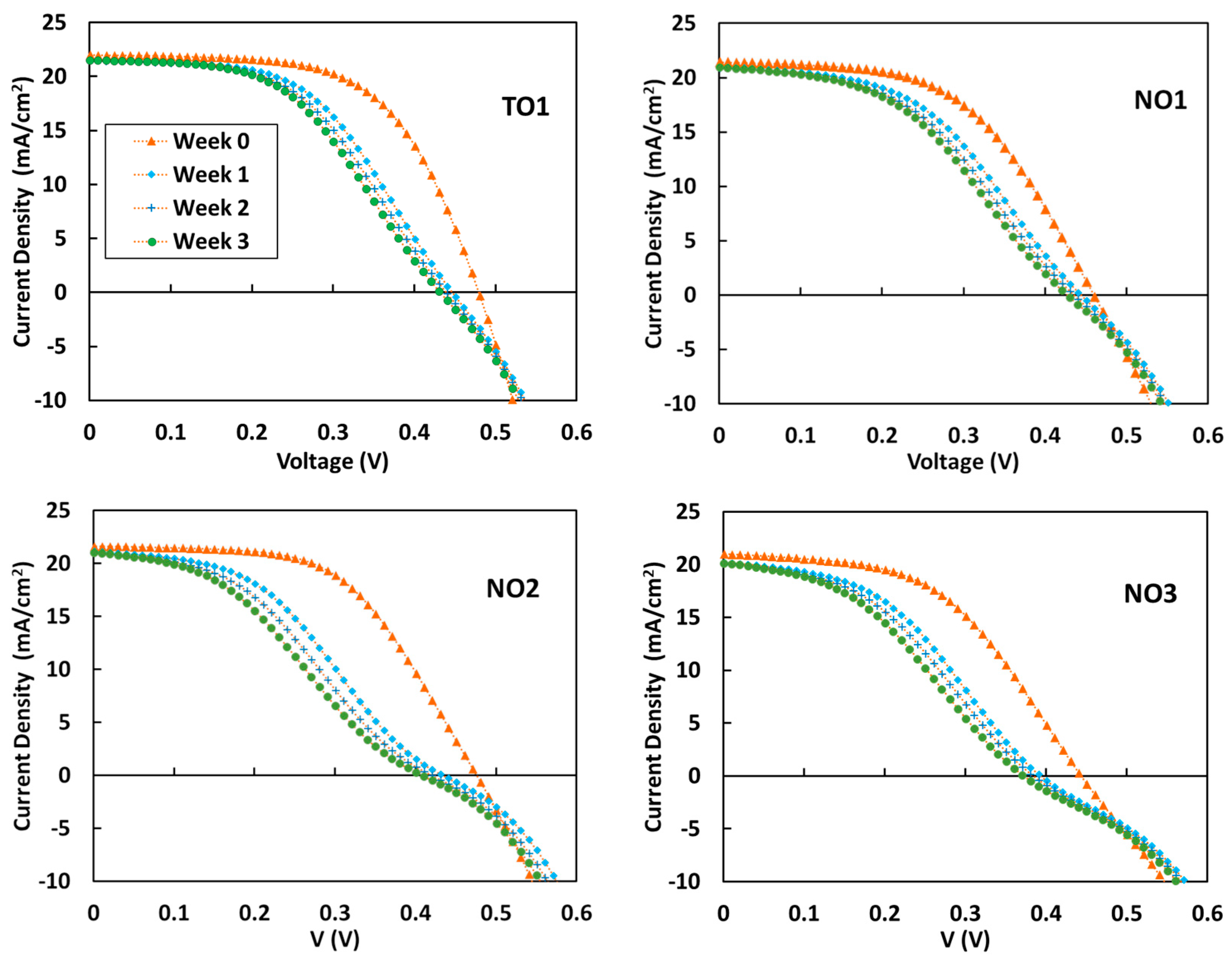
3.5. Durability of S-PEDOT/Si SOHCs

Each champion cell was stored inside a vacuum box in the dark. Figure 8 shows the durability of VOC, FF, and JSC values for the TO1, NO1, NO2, and NO3 samples over time. Each parameter was extracted from the J–V curves, which were obtained over a period of 4 weeks as shown in Figure 9. The performance of all fabricated cells degraded and developed “S-shaped” characteristics over this time period. A particular sharp change was noted for all samples at the very first week. This resulted in a reduction in VOC and an even more dramatic reduction in FF (Figure 8). The reduction in VOC was observed to be the highest in the NO3 sample (50 mV) followed by NO2 (42 mV), TO1 (33 mV), and NO1 (16 mV). In terms of FF, the NO3 sample degraded the most at 13%, and relatively equal amounts of deterioration were noted in other samples with values of 9, 8, and 7% for TO1, NO2, and NO1, respectively. After the first week, all samples degraded almost uniformly, though NO2 and NO3 seem to do so at a slightly faster rate. The NO1 samples were observed to be the most stable in this study.

4. Discussion

In this section, the role of the interfacial oxide layer, its growth, and their effects on the durability of SOHCs was widely discussed. Although the quality of the oxide layer and stability of the S-PEDOT layer are not completely understood, these properties were thought to be the primary cause for poor device performance. The effects of the quality and composition of the oxide layer has similarly been theorized. Based on all the results in the previous section, we hypothesize that the degradation observed is mainly caused by two factors: (i) the deterioration of the S-PEDOT film and (ii) thickening the oxide layer through the reaction between the silicon and atmospheric air. Regarding the former, currently, not much is known regarding the stability of S-PEDOT. On the other hand, its well-understood counterpart, PEDOT:PSS, has been known to show variance between samples based on synthesis [39,40,41]. It has also been reported that PEDOT:PSS films exhibit lower conductivity and work functions upon water absorption [24,25,42,43]. The S-PEDOT used in this study does not require any secondary doping, and it is not affected by the morphology of its film as it does not have the same granular structure [44]. Furthermore, as our samples were stored in a vacuum box, the possible effect of water absorption by the S-PEDOT was kept to a minimum. Since the annealing condition may affect its conductivity, all samples were heated at the same time using the same hotplate at 130 °C. Then, the S-PEDOT surface was immediately move to the vacuum chamber to form the finger grids and subsequently an MgF2 AR layer to prevent any problematic effects due to humidity. Our aim was to try and simulate conditions where the solar cell is well encapsulated from both air and moisture in order to narrow down the causes of degradation. Chemical oxidation of PEDOT:PSS has been known to de-dope the film through sulfur elimination [45]. Trujillo et al. [22] observed the loss of sulfur in PEDOT:PSS devices as they aged under ambient conditions and correlated it with the de-doping of the film through simulations. The behavior of our samples even under a chemically inert environment is in good agreement with the trends shown in their work. Therefore, it is likely that similar phenomena may occur in both PEDOT: PSS and S-PEDOT thin film samples through the reaction between PEDOT and the oxide interfacial layer.
Regarding the evaluation of the interfacial oxide layer, we introduced four types of interfacial oxide layers in our devices: (i) A more porous and inconsistent oxide layer (TO), (ii) more homogenous but under-saturated, thin layers (NO2 and NO3), and (iii) a highly saturated, relatively thicker (1.37 nm) layer (NO1). As shown in the EQE and JV measurements, the TO cell generates a slightly higher JSC, resulting in the highest PCE among all cells. Although no concrete explanation could be determined at the time of writing, it is possible that the more porous and uneven TO layer may have been more favorable to light-trapping. The favorable SiOx-Si band alignment is necessary in order to obtain good J–V characteristics in such hybrid devices. The optimum thickness of this oxide layer is, of course, dependent on the overall oxygen saturation and density of the layer. Simulations using an ideal, fully saturated interfacial oxide have predicted that layers less than 1 nm should exhibit good FF without producing an s-shaped J–V curve [22]. Unfortunately, to the best of our knowledge, there is currently no method to grow sub-nanometer thin, pure SiO2 films on Si without any sub-oxide interlayer. From the large drop in FF and JSC during the first week of measuring the samples, it is evident that the cause was a reduction in the doping concentration of S-PEDOT due to its reaction with the substrate and the sub-oxides and subsequent growth in the interfacial layer as similarly reported by other groups [20,22]. The rate of initial degradation for each sample seems to depend on the saturation of oxygen in the interfacial layer. This can be easily visualized using the VOC of the cells as shown in Figure 8. Three out of the four samples experienced rapid degradation within the first seven days. Here, the highest reduction in VOC is observed in the NO3 sample, which has the most sub-oxides in its interfacial layer (Figure 5c). On the other hand, the degradation trend seen for NO1 is almost linear. This drop in VOC may be correlated with the ratio of sub-oxides to the Si4+ state in the interfacial layer. A higher amount of SiO2 may lower the reaction rate of S-PEDOT with the interfacial layer, therefore, preventing its subsequent growth. The growth of this reactive oxide layer manifests as a more pronounced “bend” at the base of the J–V curves in the NO samples (Figure 7). The deterioration of the cells after week 1 seems to reduce to a lower linear rate of approximately 9.5 ± 2.8 mV/week. The largely similar trend across all the samples may point towards the same mechanism, which is likely some form of de-doping in the S-PEDOT layer. It is possible that this phenomenon is similar to the chemical oxidation predicted for PEDOT:PSS in other studies.
This study shows that a low-pressure vacuum environment cannot eliminate either the development of oxide or the loss in S-PEDOT performance. However, a high-quality and well saturated silicon dioxide layer interfacial layer can effectively passivate the substrate surface from reactive S-PEDOT. Although we were only able to achieve a minimum thickness of 1.3 nm with this type of layer, further optimization of the neutral beam process may be able to achieve thinner saturated layers. This has the potential to both improve the VOC and lifetimes of these hybrid devices for the eventual commercial deployment of this technology.

5. Conclusions

In this study, we fabricated simple planar silicon-organic hybrid solar cells (SOHCs) using a new self-doped PEDOT, which overcomes some of the limitations of PEDOT:PSS. The best performing cells achieved an efficiency of 6.35% with 397 mV in VOC and 25.82 mA/cm2 in JSC for a cell with a 1 nm-thick interfacial oxide layer. This is comparable to similarly designed PEDOT:PSS/Si solar cells reported in the literature. Ageing the samples in a low-pressure vacuum condition revealed two dominant degradation mechanisms and the development of s-shaped J–V responses: (i) reaction of S-PEDOT with unsaturated silicon sub-oxides, leading to the growth of the interstitial layer, and (ii) the degradation of S-PEDOT over time. The use of a thin, homogeneous, and highly saturated silicon oxide layer using neutral beam oxidation (NBO) proved effective against mitigating the first factor. This layer also produced much more consistent results than thermally grown oxide layers. Cells using a 1.4 nm NBO layer showed a variation in efficiency of only 0.1% compared to 1.08% seen for samples with a thermally grown oxide layer. However, separating the individual effects of the degradation factors, such as the exact cause for the loss in S-PEDOT performance, was beyond the scope of this research. Such studies may involve measuring the cells under a nitrogen environment and encapsulation of the device. The overall efficiency of the cell itself has great room for improvement through the use of nano-texturing, better light trapping, and possibly through the use of multi-junction devices. Many of these options will be further explored in future research.

Author Contributions

Conceptualization, A.S.; investigations and methodology, A.S. and R.O.; data curation, R.O.; formal analysis, A.S., R.O., D.O., K.E. and T.S.; synthesis and characterization of S-PEDOT, H.O. and H.Y.; resources, S.S. and H.Y.; writing—original draft preparation, A.S.; writing—review and editing, A.S., R.O. and T.S.; supervision, T.T. All authors have read and agreed to the published version of the manuscript.

Funding

This study was partly supported by Grants-in-Aid for Scientific Research (Grants No. 21K18591) from the Japan Society for the Promotion of Science.

Data Availability Statement

The data presented in this study are available on request from the corresponding author.

Conflicts of Interest

The authors declare no conflict of interest.

References

  1. Arias, P.A.; Bellouin, N.; Jones, R.G.; Naik, V.; Plattner, G.-K.; Rogelj, J.; Sillmann, J.; Storelvmo, T.; Thorne, P.W.; Trewin, B.; et al. Technical Summary. Clim. Chang. 2021, 51, 221–227. [Google Scholar]
  2. Höller, R.; Gudopp, D.; Leschinsky, T. Solar PV Cost Reduction Potential in Japan. Preprints 2019, 2019040065. [Google Scholar] [CrossRef]
  3. Kimura, K. Solar Power Generation Costs in Japan. Available online: https://www.renewable-ei.org/en/activities/reports/20211014.php (accessed on 3 May 2023).
  4. Matsui, T.; Bivour, M.; Hermle, M.; Sai, H. Atomic-Layer-Deposited TiOx Nanolayers Function as Efficient Hole-Selective Passivating Contacts in Silicon Solar Cells. ACS Appl. Mater. Interfaces 2020, 12, 49777–49785. [Google Scholar] [CrossRef]
  5. Poorkazem, K.; Liu, D.; Kelly, T.L. Fatigue Resistance of a Flexible, Efficient, and Metal Oxide-Free Perovskite Solar Cell. J. Mater. Chem. A 2015, 3, 9241–9248. [Google Scholar] [CrossRef]
  6. Chen, L.; Xie, X.; Liu, Z.; Lee, E.-C. A Transparent Poly(3,4-Ethylenedioxylenethiophene):Poly(Styrene Sulfonate) Cathode for Low Temperature Processed, Metal-Oxide Free Perovskite Solar Cells. J. Mater. Chem. A 2017, 5, 6974–6980. [Google Scholar] [CrossRef]
  7. Dianetti, M.; Di Giacomo, F.; Polino, G.; Ciceroni, C.; Liscio, A.; D’Epifanio, A.; Licoccia, S.; Brown, T.M.; Di Carlo, A.; Brunetti, F. TCO-Free Flexible Organo Metal Trihalide Perovskite Planar-Heterojunction Solar Cells. Sol. Energy Mater. Sol. Cells 2015, 140, 150–157. [Google Scholar] [CrossRef]
  8. Ma, Y.; Chen, S.-C.; Wang, Z.; Ma, W.; Wang, J.; Yin, Z.; Tang, C.; Cai, D.; Zheng, Q. Indacenodithiophene-Based Wide Bandgap Copolymers for High Performance Single-Junction and Tandem Polymer Solar Cells. Nano Energy 2017, 33, 313–324. [Google Scholar] [CrossRef]
  9. Prosa, M.; Tessarolo, M.; Bolognesi, M.; Cramer, T.; Chen, Z.; Facchetti, A.; Fraboni, B.; Seri, M.; Ruani, G.; Muccini, M. Efficient and Versatile Interconnection Layer by Solvent Treatment of PEDOT:PSS Interlayer for Air-Processed Organic Tandem Solar Cells. Adv. Mater. Interfaces 2016, 3, 1600770. [Google Scholar] [CrossRef]
  10. Okamoto, K.; Kishibe, K.; Sano, N.; Tanabe, K. PEDOT:PSS-Mediated Semiconductor Wafer Bonding for Built-in Middle Subcells in Multijunction Solar Cells. Appl. Phys. Express 2023, 16, 036502. [Google Scholar] [CrossRef]
  11. Yoon, S.-S.; Khang, D.-Y. High Efficiency (>17%) Si-Organic Hybrid Solar Cells by Simultaneous Structural, Electrical, and Interfacial Engineering via Low-Temperature Processes. Adv. Energy Mater. 2018, 8, 1702655. [Google Scholar] [CrossRef]
  12. Hu, W.; Igarashi, M.; Lee, M.-Y.; Li, Y.; Samukawa, S. Realistic Quantum Design of Silicon Quantum Dot Intermediate Band Solar Cells. Nanotechnology 2013, 24, 265401. [Google Scholar] [CrossRef]
  13. Shi, H.; Liu, C.; Jiang, Q.; Xu, J. Effective Approaches to Improve the Electrical Conductivity of PEDOT:PSS: A Review. Adv. Electron. Mater. 2015, 1, 1500017. [Google Scholar] [CrossRef]
  14. Yamashita, M.; Otani, C.; Shimizu, M.; Okuzaki, H. Effect of Solvent on Carrier Transport in Poly(3,4-Ethylenedioxythiophene)/Poly(4-Styrenesulfonate) Studied by Terahertz and Infrared-Ultraviolet Spectroscopy. Appl. Phys. Lett. 2011, 99, 143307. [Google Scholar] [CrossRef]
  15. Ouyang, J.; Xu, Q.; Chu, C.-W.; Yang, Y.; Li, G.; Shinar, J. On the Mechanism of Conductivity Enhancement in Poly(3,4-Ethylenedioxythiophene):Poly(Styrene Sulfonate) Film through Solvent Treatment. Polymer 2004, 45, 8443–8450. [Google Scholar] [CrossRef]
  16. Kim, J.Y.; Jung, J.H.; Lee, D.E.; Joo, J. Enhancement of Electrical Conductivity of Poly(3,4-Ethylenedioxythiophene)/Poly(4-Styrenesulfonate) by a Change of Solvents. Synth. Met. 2002, 126, 311–316. [Google Scholar] [CrossRef]
  17. Nardes, A.M.; Janssen, R.A.J.; Kemerink, M. A Morphological Model for the Solvent-Enhanced Conductivity of PEDOT:PSS Thin Films. Adv. Funct. Mater. 2008, 18, 865–871. [Google Scholar] [CrossRef]
  18. Jönsson, S.K.M.; Birgerson, J.; Crispin, X.; Greczynski, G.; Osikowicz, W.; Denier Van Der Gon, A.W.; Salaneck, W.R.; Fahlman, M. The Effects of Solvents on the Morphology and Sheet Resistance in Poly(3,4-Ethylenedioxythiophene)–Polystyrenesulfonic Acid (PEDOT–PSS) Films. Synth. Met. 2003, 139, 1–10. [Google Scholar] [CrossRef]
  19. Venkatesan, R.; Sheik Kadar Maideen, S.M.T.; Chandhiran, S.; Kushvaha, S.S.; Sagadevan, S.; Venkatachalapathy, V.; Mayandi, J. Fabrication and Characterization of Si/PEDOT: PSS-Based Heterojunction Solar Cells. Electronics 2022, 11, 4145. [Google Scholar] [CrossRef]
  20. Jäckle, S.; Liebhaber, M.; Niederhausen, J.; Büchele, M.; Félix, R.; Wilks, R.G.; Bär, M.; Lips, K.; Christiansen, S. Unveiling the Hybrid N-Si/PEDOT:PSS Interface. ACS Appl. Mater. Interfaces 2016, 8, 8841–8848. [Google Scholar] [CrossRef]
  21. He, L.; Jiang, C.; Wang, H.; Lai, D. Rusli High Efficiency Planar Si/Organic Heterojunction Hybrid Solar Cells. Appl. Phys. Lett. 2012, 100, 073503. [Google Scholar] [CrossRef]
  22. Angel Trujillo, D.A.; Iyer, A.; Hack, J.; Opila, R.L. Role of Oxide at Interface between Organic Layer and Silicon Substrate in Hybrid Solar Cells. J. Mater. Res. 2021, 36, 557–570. [Google Scholar] [CrossRef]
  23. Yano, H.; Kudo, K.; Marumo, K.; Okuzaki, H. Fully Soluble Self-Doped Poly(3,4-Ethylenedioxythiophene) with an Electrical Conductivity Greater than 1000 S cm−1. Sci. Adv. 2019, 5, eaav9492. [Google Scholar] [CrossRef]
  24. Muckley, E.S.; Jacobs, C.B.; Vidal, K.; Mahalik, J.P.; Kumar, R.; Sumpter, B.G.; Ivanov, I.N. New Insights on Electro-Optical Response of Poly(3,4-Ethylenedioxythiophene):Poly(Styrenesulfonate) Film to Humidity. ACS Appl. Mater. Interfaces 2017, 9, 15880–15886. [Google Scholar] [CrossRef] [PubMed]
  25. Dupont, S.R.; Novoa, F.; Voroshazi, E.; Dauskardt, R.H. Decohesion Kinetics of PEDOT:PSS Conducting Polymer Films. Adv. Funct. Mater. 2014, 24, 1325–1332. [Google Scholar] [CrossRef]
  26. Sheng, J.; Fan, K.; Wang, D.; Han, C.; Fang, J.; Gao, P.; Ye, J. Improvement of the SiOx Passivation Layer for High-Efficiency Si/PEDOT:PSS Heterojunction Solar Cells. ACS Appl. Mater. Interfaces 2014, 6, 16027–16034. [Google Scholar] [CrossRef]
  27. Kumari, P.; Sharma, R.K.; Srivastava, A.; Srivastava, S.K. Effect of ZnO BSF Layer on the Performance of PEDOT:PSS/Si Heterojunction Solar Cell. Mater. Today Proc. 2023, 82, 158–162. [Google Scholar] [CrossRef]
  28. Thomas, J.P.; Zhao, L.; Abd-Ellah, M.; Heinig, N.F.; Leung, K.T. Interfacial Micropore Defect Formation in PEDOT:PSS-Si Hybrid Solar Cells Probed by TOF-SIMS 3D Chemical Imaging. Anal. Chem. 2013, 85, 6840–6845. [Google Scholar] [CrossRef]
  29. Oshima, R.; Watanabe, Y.; Yamanaka, M.; Kawanami, H.; Sakamoto, I.; Matsubara, K.; Sakata, I. High-Quality SiGe Films Grown with Compositionally Graded Buffer Layers for Solar Cell Applications. J. Cryst. Growth 2013, 378, 226–229. [Google Scholar] [CrossRef]
  30. Knotter, D.M. Etching Mechanism of Vitreous Silicon Dioxide in HF-Based Solutions. J. Am. Chem. Soc. 2000, 122, 4345–4351. [Google Scholar] [CrossRef]
  31. Nielsen, H.; Hackleman, D. Some Illumination on the Mechanism of SiO2 Etching in HF Solutions. J. Electrochem. Soc. 1983, 130, 708–712. [Google Scholar] [CrossRef]
  32. Biesinger, M.C. Accessing the Robustness of Adventitious Carbon for Charge Referencing (Correction) Purposes in XPS Analysis: Insights from a Multi-User Facility Data Review. Appl. Surf. Sci. 2022, 597, 153681. [Google Scholar] [CrossRef]
  33. Niimi, H.; Yang, H.; Lucovsky, G.; Keister, J.W.; Rowe, J.E. Barrier Layer Model Determined by XPS Data for Tunneling Current Reductions at Monolayer Nitrided Si–SiO2 Interfaces. Appl. Surf. Sci. 2000, 166, 485–491. [Google Scholar] [CrossRef]
  34. Khalilov, U.; Pourtois, G.; Huygh, S.; Van Duin, A.C.T.; Neyts, E.C.; Bogaerts, A. New Mechanism for Oxidation of Native Silicon Oxide. J. Phys. Chem. C 2013, 117, 9819–9825. [Google Scholar] [CrossRef]
  35. Sato, R.; Wasai, Y.; Izumi, Y.; Ueno, K.; Shirai, H. Influence of Effective Mass on Carrier Concentration for PEDOT:PSS and S-PEDOT Thin Films Studied by Ellipsometry and Hall Measurement. J. Phys. Chem. C 2023, 127, 13196–13206. [Google Scholar] [CrossRef]
  36. Schmidt, J.; Titova, V.; Zielke, D. Organic-Silicon Heterojunction Solar Cells: Open-Circuit Voltage Potential and Stability. Appl. Phys. Lett. 2013, 103, 183901. [Google Scholar] [CrossRef]
  37. Yameen, M.; Srivastava, S.K.; Singh, P.; Prathap, P.; Vandana; Rauthan, C.M.S.; Singh, P.K. Stability Study of PEDOT:PSS/Micro-Textured Silicon Hetero-Junction Solar Cells. Adv. Sci. Lett. 2014, 20, 1540–1544. [Google Scholar] [CrossRef]
  38. Hossain, J.; Mondal, B.K.; Mostaque, S.K.; Ahmed, S.R.A.; Shirai, H. Optimization of Multilayer Anti-Reflection Coatings for Efficient Light Management of PEDOT:PSS/c-Si Heterojunction Solar Cells. Mater. Res. Express 2020, 7, 015502. [Google Scholar] [CrossRef]
  39. Koch, N.; Vollmer, A.; Elschner, A. Influence of Water on the Work Function of Conducting Poly(3,4-Ethylenedioxythiophene)/Poly(Styrenesulfonate). Appl. Phys. Lett. 2007, 90, 043512. [Google Scholar] [CrossRef]
  40. Huang, J.; Miller, P.F.; Wilson, J.S.; De Mello, A.J.; De Mello, J.C.; Bradley, D.D.C. Investigation of the Effects of Doping and Post-Deposition Treatments on the Conductivity, Morphology, and Work Function of Poly(3,4-Ethylenedioxythiophene)/Poly(Styrene Sulfonate) Films. Adv. Funct. Mater. 2005, 15, 290–296. [Google Scholar] [CrossRef]
  41. Yun, D.-J.; Ra, H.; Kim, J.; Hwang, I.; Lee, J.; Rhee, S.-W.; Chung, J. Characterizing Annealing Effect of Poly (3,4-Ethylenedioxythiophene) Polymerized with Poly (4-Styrenesulfonate) Conjugated Film on the Molecular Arrangement and Work Function by Core-Level and Valence-Level Band Spectra. ECS J. Solid State Sci. Technol. 2012, 1, M10–M14. [Google Scholar] [CrossRef]
  42. Nardes, A.M.; Kemerink, M.; De Kok, M.M.; Vinken, E.; Maturova, K.; Janssen, R.A.J. Conductivity, Work Function, and Environmental Stability of PEDOT:PSS Thin Films Treated with Sorbitol. Org. Electron. 2008, 9, 727–734. [Google Scholar] [CrossRef]
  43. Bailo, D.; Generosi, A.; Albertini, V.R.; Caminiti, R.; De Bettignies, R.; Paci, B. Time-Resolved Morphological Study of ‘PEDOT:PSS’ Hole Transporting Layer for Polymer Solar Cells. Synth. Met. 2012, 162, 808–812. [Google Scholar] [CrossRef]
  44. Gutierrez-Fernandez, E.; Ezquerra, T.A.; García-Gutiérrez, M.-C. Additive Effect on the Structure of PEDOT:PSS Dispersions and Its Correlation with the Structure and Morphology of Thin Films. Polymers 2021, 14, 141. [Google Scholar] [CrossRef] [PubMed]
  45. Fan, J.; Rezaie, S.S.; Facchini-Rakovich, M.; Gudi, D.; Montemagno, C.; Gupta, M. Tuning PEDOT:PSS Conductivity to Obtain Complementary Organic Electrochemical Transistor. Org. Electron. 2019, 66, 148–155. [Google Scholar] [CrossRef]
Figure 1. (a) SEM image of a PEDOT:PSS layer deposited on 80 nm-tall Si nanocones. PEDOT:PSS is unable to penetrate through the nanocones as the colloidal particles are larger than the average pitch between two cones. (b) SEM image shows S-PEDOT deposited on the same type of nanocones.
Energies 16 06900 g001
Figure 2. Architecture of the Si/S-PEDOT solar cell fabricated in this work.
Energies 16 06900 g002
Figure 3. Normalized absorbance spectra of S-PEDOT (80 nm thick) and PEDOT:PSS secondary doped with 3% EG (120 nm thick).
Energies 16 06900 g003
Figure 4. (a) Bird’s eye view and (b) cross-sectional SEM images of an S-PEDOT layer coated on the non-polished rough silicon surface. (c,d) show AFM images of the topmost S-PEDOT and PEDOT:PSS surfaces formed on the non-polished rough silicon surface, respectively. The scan size is 500 nm × 500 nm.
Energies 16 06900 g004aEnergies 16 06900 g004b
Figure 5. Si 2s spectra (red line) of silicon substrates with a neutral beam interfacial oxide layer with the fitted peaks of the sub-oxide components. The SiOx layer was chemically etched using HF for (a) 30 s (NO1), (b) 40 s (NO2), and (c) 50 s (NO3).
Energies 16 06900 g005
Figure 6. Illuminated J–V curves for each champion SOHC with different interfacial oxide layers. All cells except the TO1 (PEDOT:PSS) cell were coated with S-PEDOT.
Energies 16 06900 g006
Figure 7. (a) EQE spectra for S-PEDOT/Si cells with different thicknesses of the neutral beam oxide (NO) interlayer. (b) shows EQE spectra for TO1 and NO2 cells with 1.07 nm and 1.03 nm-thick interlayers, respectively.
Energies 16 06900 g007
Figure 8. Durability of (a) JSC, (b) FF, and (c) VOC of the TO1, NO1, NO2, and NO3 samples over time.
Energies 16 06900 g008
Figure 9. Illuminated J−V characteristics of the each SOHCs with different interfacial oxide layers over 4 weeks.
Energies 16 06900 g009
Table 1. Summary of solar cell parameters for planar SOHCs with a SiOx layer at the interface.
Device StructureVOC
(mV)
JSC (mA/cm2)FF
(%)
PCE
(%)
Ref.
Ag/S-PEDOT/SiOx/Si/Au-Sb/Au48222.061.06.35This work
Au/PEDOT:PSS/SiOx/Si/In:Ga54830.573.012.2[20]
Ag/PEDOT:PSS/SiOx/Si/Ti/Pd/Ag58025.862.49.4[21]
Ag/PEDOT:PSS/SiOx/Si/Ti-Ag49033.264.510.48[26]
Ag/PEDOT:PSS/SiOx/Si/n-ZnO/In:Ga50822.251.75.84[27]
Ag/PEDOT:PSS/SiOx/Si/Al51024.341.25.08[28]
Table 2. Oxygen saturation and film thickness of interfacial oxide films.
SamplePreparationThickness (nm)Oxygen Saturation (%)
NBONBO for 400 s4.6295
NO130 s HF etch after NBO1.3783
NO240 s HF etch after NBO1.0343
NO350 s HF etch after NBO0.5255
TO1150 °C for 15 min1.0754
Table 3. Solar cell parameters for PEDOT:PSS/Si and S-PEDOT/Si SOHCs fabricated using different interfacial oxide layers.
SOHCVOC (mV)JSC (mA/cm2)FF (%)PCE (%)
NO1453.25 ± 6.7521.41 ± 0.2850.25 ± 34.92 ± 0.33
(Best)(460.00)(21.69)(53.00)(5.25)
NO2474.25 ± 8.7521.73 ± 0.4554 ± 25.59 ± 0.10
(Best)(483.00)(22.18)(56.00)(5.69)
NO3419.5 ± 13.5021.25 ± 0.7049.5 ± 0.54.43 ± 0.2
(Best)(433.00)(21.95)(50.00)(4.63)
TO1460 ± 22.0021.54 ± 0.4555 ± 65.53 ± 0.82
(Best) (482.00) (21.99) (61.00) (6.35)
TO1 (PEDOT:PSS)270 ± 127.0025.02 ± 0.7838.40 ± 3.863.25 ± 1.08
(Best)(397.00)(25.82)(42.26)(4.33)
Disclaimer/Publisher’s Note: The statements, opinions and data contained in all publications are solely those of the individual author(s) and contributor(s) and not of MDPI and/or the editor(s). MDPI and/or the editor(s) disclaim responsibility for any injury to people or property resulting from any ideas, methods, instructions or products referred to in the content.

