Review

Review, Comprehensive Analysis and Derivation of Analytical Power Loss Calculation Equations for Two- to Three-Level Midpoint Clamped Inverter Topologies with Hybrid Switch Configurations

Institute for Electrical Machines, Traction and Drives, Technische Universität Braunschweig, 38106 Braunschweig, Germany
*
Author to whom correspondence should be addressed.
Energies 2023, 16(18), 6710; https://doi.org/10.3390/en16186710
Submission received: 14 August 2023 / Revised: 7 September 2023 / Accepted: 13 September 2023 / Published: 19 September 2023
(This article belongs to the Section F3: Power Electronics)

Abstract

:
Increased performance requirements in new power electronics areas of application, such as electric aircraft, make innovations on different design levels necessary. In order to quickly compare different topologies, analytical loss equations provide a fast and straightforward way to narrow down the possible solution space. The approach widely used in the literature results in long and complex terms, which can only be compared between different literature sources with great effort. Moreover, the literature lacks a detailed summarizing description of these analytical equations and their derivation, starting from the standard two-level VSI up to three-level midpoint clamped inverter topologies, such as the ANPC topology in its different modulation schemes. The application of such higher-level inverter topologies allows hybrid device configurations to become performant solutions. This work aims to give a closed-form description of the analytical loss modeling and the theoretical background and provide an implementation approach for a wide span of inverter topologies and for different modulation methods.

1. Introduction

In power electronics, increasing converter performance and thus entering new application areas is usually achieved by the introduction of new building blocks for converter design. Such building blocks can be, for example, new components, topologies, or control schemes. The benefits that can be achieved are always limited by the current state of research and, thus, availability. Examples of novel power components are new or significantly improved semiconductors, but also magnetics, capacitors, or cooling solutions [1]. On the semiconductor side, this includes novel switch types, such as the high-electron-mobility transistor (HEMT) [2]; materials, such as wide-bandgap (WBG) materials (currently primarily SiC and GaN); and novel packaging options. As innovative novel topologies, the H5 topology for PV inverters [3] or the ANPC topology [4] (Figure 1) can be named. Beyond this, the integration of, e.g., emerging semiconductors and existing topologies offers new solutions for challenges faced in new areas of application.
One such application area currently being strongly researched is the electrification of aircraft, where global mobility is increasingly confronted with the societal need to reduce the impact of air travel on the environment significantly. The proposed solutions in this sector range from the electrification of some peripheral systems, such as pneumatic loads in so-called More Electric Aircraft (MEA), to All-Electric Aircraft (AEA), where all thrust components are replaced by electric machines [5].
The set of required performance parameters for this novel application area is shown in Figure 2. In aerospace applications, efficiency, size (weight and volume), reliability, and electromagnetic compatibility (EMC), as well as electromagnetic interference (EMI), are especially pronounced. Power electronics in general and the drive inverters play a crucial role in interconnecting sources and loads as part of the electric energy distribution system. They have to be designed in such a way that they can contribute to these goals while functioning in the overall system.
Generally speaking, the electric system of an AEA is expected to be characterized by the presence of a high DC voltage, and a high inverter output power will be required. DC voltages are preferred to decouple sources and loads, and high voltages are preferred for the transmission of high power because, in this way, the current per conductor and, with it, the conductor diameter is decreased. This reduces the system weight and contributes to a higher overall power density [5]. Furthermore, high requirements on the efficiency and power density of the inverter itself, as well as the inverter output power quality, prevail.
The use of new WBG semiconductor devices is particularly attractive for aerospace applications, where efficiency and power density are of primary concern. The use of WBG components enables the efficient utilization of higher switching frequencies and, thus, a reduction in the size of passive components.
However, using WBG devices in variable-speed drive applications also poses some challenges. The fast switching transitions at the inverter output can have a negative impact on the driven electrical machine. Either additional stress and losses in the machine are imposed, or the effect is counteracted by dedicated filtering at the inverter output, which in turn negatively affects the power density of the system [7].
Further, the application of such WBG devices is hindered by high DC link voltages, which require the use of switches with high breakdown voltages, especially in aerospace applications, where an additional voltage safety margin has to be considered due to, for example, cosmic radiation. In particular, for the emerging WBG devices, where development is not as advanced in terms of breakdown voltages (see Table 1), multi-level topologies, which do not stress the individual switches with the full DC link voltage, could be used. In the following, neutral-point clamped—more specifically, three-level midpoint clamped—topologies will be discussed.
Besides these neutral-point clamped-type topologies, which are being most frequently investigated for electric aircraft applications due to their high power densities [9,10], other topologies such as multi-level flying capacitor (FC) converters, modular multi-level converters (MMCs), or cascaded H-bridge multi-level inverters (CHBs) exist. Cascaded H-bridge multi-level inverters (CHBs) consist of multiple single-phase H-bridges connected in a cascade. The modular setup allows a cost reduction. The CHB topology requires an isolated DC power supply per H-bridge power cell, necessitating additional circuit hardware [11]. Modular multi-level converters (MMCs) consist of series connections of half bridges, each in the upper and lower leg branches. However, especially for weight-sensitive application areas, the required branch inductors increase the converter weight significantly, resulting in low power density compared to the other topologies [9]. Multi-level inverters with flying capacitors (FC) [12] represent another important type of multi-level topology. In this topology, so-called flying capacitor cells are connected by a capacitor [13]. Increasing the number of steps in the AC output voltage is possible by adding more flying capacitor cells and capacitors. Extra passive components are required, which compromise the converter power density, especially because every flying capacitor is sequentially charged and discharged with the load current [14]. The suitability of FC converters for aviation is deemed critical due to the additional weight and reduced reliability associated with the flying capacitors, and they, therefore, are not considered in this work. To overcome the inherent limitations of this topology, innovative control strategies and sophisticated hardware designs are required. To take advantage of GaN semiconductors by using these devices in combination with a high voltage level count [15,16,17] and in combination with interleaving to increase the power rating [18], this topology can be applicable.
In order to increase the power density and efficiency of the overall system, multi-level topologies, as well as novel WBG power semiconductors that enable high-frequency switching, must be employed. The following work is intended to help to identify inverter topologies and devices to be used in order to unlock their full potential.
For the prediction of losses and, therefore, efficiency in power semiconductors, various methods exist. One possibility is the complete numerical simulation of the circuit. This allows detailed information to be obtained not only in terms of efficiency but also, for example, to investigate the influence of parasitic elements. However, the disadvantage of this approach is that computational resources are required, and the simulations can take a long time [19]. To quickly compare different topologies utilizing different types of switches, analytical models provide a fast and straightforward way to narrow down the possible solution space. The most widely used approach to the setup of these analytical equations is the use of conduction as well as switching intervals and modulation functions in combination with device parameters that can be obtained easily from the manufacturer’s data sheets.
In [9], analytical loss equations are used to establish an analytical efficiency and power density model for a study on future all-electric aircraft propulsion systems. However, the derivation, explanation, and application of these equations are not part of this work. Furthermore, the different active neutral-point clamped (ANPC) modulation schemes are not fully discussed. Ref. [20] presents analytical loss calculation expressions for the semiconductor devices in a T-type neutral-point clamped (TNPC) topology and proposes a loss-balancing scheme for this topology. Equations for the conventional neutral-point clamped (NPC) topology are also provided.
In [21], a comprehensive overview of various ANPC modulation schemes and associated analytical power dissipation equations is provided. The microcontroller implementation of the pulse width modulation (PWM) channels is discussed, and state diagrams are provided for the different modulation strategies, also discussing the transitions between the switching states.
Publication [22] discusses the analytical approach to determining the converter’s efficiency. However, as in [21], the motivation for using such multi-level inverter topologies, as well as much of the theoretical background, is not discussed. In addition, the two-level voltage source inverter (VSI) or the TNPC topology is not discussed in detail. This would be desirable for comparison reasons and a more complete overview of the inverter landscape.
The modeling in [23] includes the standard two-level inverter, as well as TNPC and NPC topologies for hybrid switch configurations. However, the ANPC topology and its associated degrees of freedom in different modulation strategies are not considered. Meanwhile, ref. [24] utilizes analytical equations for the power loss modeling of a GaN HEMT-based three-level ANPC inverter for different PWM techniques. While it provides a good overview of the different carrier-based modulation techniques (comparable to the one in [25]), only unipolar devices are considered, and switching loss calculation is simplified.
While all publications refer to the use of part of the analytical loss equations discussed in this work, not all provide a closed set of complete equations or the complete disclosure of the modulation functions and conduction intervals to be applied. Research that, in a closed form, examines the theoretical background and provides implementation approaches while covering the range from standard two-level VSI topologies up to the three-level ANPC topology in its various modulation schemes, does not exist.
Despite requiring significantly fewer data than numerical models, one distinct disadvantage of the analytical power loss calculation approach for multi-level inverters is that they quickly result in long and complex terms. The integration that has to be performed to obtain the loss equations (see Section 4) is both prone to human error and time-consuming to implement. The equations’ implementation has to be performed with great care. To aid this, this publication aims to establish a shared foundation for the understanding and cross-verification of the analytical power loss calculations of two- to three-level topologies.
In the first section, a general introduction to the motivation in using multi-level inverter topologies is given. In Section 2, this work provides a comprehensive overview of the most widespread midpoint clamped three-level topologies and the conventional two-level VSI as a reference. Their general setup, advantages, and disadvantages are discussed. With respect to the extended degrees of freedom and, therefore, the capabilities offered by the ANPC topology, the inverter modulation methods and schemes are discussed in Section 3. Section 4 aims to offer a deep understanding of the fundamentals of analytical power loss calculation for each topology and for different pulse width modulation methods. Modulation functions, conduction as well as switching intervals, and the obtainment of the analytical loss formulas through integration are reviewed in detail. In Section 5, design, packaging, and thermal aspects for the realization of such (multi-level) inverters are discussed. Using the previously described approach, power loss analysis is performed for different topologies, (hybrid) device configurations, and modulation schemes. Section 6 concludes and provides readers with potential future research directions.

2. Inverter Circuit Topology

Different inverter topologies can be grouped and characterized according to a variety of properties. One possible means of classifying these topologies is by the design of the DC link, especially the DC link’s number of discrete voltage levels. In theory, e.g., to improve the inverter output voltage quality, high-number-level topologies exist. In practice, however, a compromise must be found between the achievable benefits and resulting complexity. In this work, two- to three-level midpoint clamped topologies will be reviewed. This selection has been explained in Section 1.
In the following sections, first, the standard two-level VSI topology and subsequently the three-level midpoint clamped topologies shown in Figure 1 will be discussed. For the reasons stated above, the previously named topologies are not considered suitable for higher-power and weight-sensitive applications and are therefore not part of the following analysis.

2.1. Two-Level Topologies

Standard Two-Level Voltage Source Inverter

The standard inverter topology used today is the two-level voltage source inverter (VSI). With a few exceptions (such as applications related to photovoltaics [26]), this topology is commonly used in the industrial sector, e.g., to drive electrical machines through DC busses [27]. The main reasons for its widespread use are its minimal component count, simplicity, and therefore cost [28]. However, the blocking voltage of the applied semiconductors has to be as large as or larger than the DC bus voltage. In general, a higher blocking voltage results in increased switching loss (for a fixed current/voltage combination), which is due to the non-linear relation between the blocking voltage and switching energy (see Figure 3). This leads to a reduction in the efficiency of this topology for higher switching frequencies due the increased switching losses [29]. Because the overall goal generally is efficient converters, a lower switching frequency could be used to decrease the power losses. However, when broadening the view from efficiency alone to other performance measures, such as volume and weight, the size reduction of passive components to achieve a high power density mainly is achieved by higher switching frequencies. For two reasons, the application of emerging wide-bandgap (WBG) semiconductors in this two-level topology is challenging. First, one prominent advantage when applying WBG power semiconductors is the allowable decrease in the size of passive devices through a higher switching frequency [29]. Moreover, a high blocking voltage requirement limits the applicability of these promising technologies, which generally still have lower breakdown voltages compared to their silicon counterparts (see Table 1).
Especially for aerospace applications, these limitations are challenging. A higher DC link voltage, which results in lighter cables or loss and higher power density, and is therefore desired, is difficult to achieve with the use of WBG power devices. Moreover, the required low switching frequency for the efficient operation of the two-level VSI, and its poor output voltage quality, make heavy and bulky passive filter components necessary. The intrinsically higher EMI noise emissions at the inverter output are problematic [28] due to strict regulations in this application area.
Introducing more than two voltage levels in so-called multi-level inverters helps to address the challenges previously mentioned. A lower breakdown voltage requirement allows for the use of low-voltage-rating WBG semiconductors. Since the inverter output voltage is generated in steps depending on the level number, its waveform approximates the desired sinusoidal shape more closely. Due to the lower dependence of the inverter efficiency on the switching frequency [32], high-frequency operation and its associated benefits are feasible.
On the machine side, introducing another voltage level is beneficial in many ways. Three-level topologies contain lower harmonic content in the AC output [9,27]. Reduced d v / d t at the motor terminal leads to less electrical stress on the motor insulation [33]. Overvoltages at motor terminals are reduced, because the less steep rising and falling edges mitigate the impedance mismatch, which would otherwise cause problematic reflection phenomena along the cable [15]. Moreover, unwanted bearing currents and shaft voltages are reduced [34].
On the other hand, multi-level inverters feature a higher part count, increased complexity, and therefore higher initial costs. Additional gate drives are needed as the number of semiconductor switches increases and, due to the more possible switching states [35], the modulation method that generates the control signals for the inverter is also more complex. Issues such as DC link balancing or the selection of redundant space vectors in the case of ANPC space-vector modulation [36] arise. DC link balancing is not discussed in this paper. However, it may be mentioned that greater freedom in the choice of different redundant switching states allows for better controllability of the DC link imbalance (see Section 3.2).
A large number of multi-level topologies are described in the literature and each topology has its own advantages and disadvantages. In theory, the number of levels could be high, but, in practice, a compromise must be found between the resulting benefits and increasing complexity. In this study, three-level midpoint clamped inverter topologies will be discussed in detail. The following Section 2.2 aims to explore their characteristics and give an insight into the topologies’ functioning principles.

2.2. Three-Level Topologies

2.2.1. Neutral-Point Clamped (NPC) Converter

A three-level NPC converter phase leg using MOSFETs is shown in Figure 1b. In comparison to the previously discussed two-level inverter, this topology, proposed first in [37], employs two extra semiconductor switches with their associated freewheeling diodes and clamps the neutral point to the phase output using two extra so-called clamping diodes. This configuration allows the required blocking voltage to be divided between two devices (T1 and T2 or T3 and T4). For standard two-level VSI, the general consensus suggests a blocking voltage of 1 / 2 up to 2 / 3 larger than the DC bus voltage, which is due to expected voltage overshoots and, especially in aircraft applications, also the influence of cosmic radiation [5]. In a three-level NPC converter, however, 650 V or 1200 V semiconductors can be considered suitable, or, for DC link voltages, 800 V or 1500 V, respectively [35]. Both of these voltage levels are repeatedly named values when discussing future electric aircraft energy systems. Given its additional voltage level, an NPC inverter’s AC output current THD and d v / d t can be reduced in comparison to two-level topologies. This, however, comes at the cost of a more sophisticated switching pattern, and an imbalance in losses for the different switching positions occurs. The switch positions heat up differently and losses concentrate at certain positions [20]. All three-level inverter topologies, influenced by the different modulation strategies, are faced with the issue of DC link capacitor voltage balance, which, influenced by the different modulation strategies, has different effects on the charging and discharging of the DC link series capacitors. Different voltage ripples in these capacitors result in different losses. However, in this article, only the losses of the active switching devices are studied, and therefore the problem of DC link imbalance is not discussed further. Without additional measures, DC link imbalance issues generally lead to larger required DC link capacitance [27,29], which increases this component’s weight.

2.2.2. T-Type Neutral-Point Clamped (TNPC) Converter

The T-type NPC converter is shown in Figure 1c as well. This topology can be seen as a two-level VSI, extended by a bidirectional switch connecting the DC link capacitor’s midpoint to the phase output, combining the two-level VSI’s advantages (e.g., low conduction losses) with the three-level NPC converter’s benefits [27]. While the upper (high-side) and lower (low-side) switches still have to block at least the full DC link voltage, the bidirectional switch is subjected to only half the DC link voltage. This reduced required blocking voltage results in acceptable conduction losses despite the series connection of two devices and low switching losses in the middle switch [20] (see Figure 3). Moreover, only one switch at a time has to block the full DC link voltage in this topology; therefore, the conduction losses in this current path can be reduced. The same switching pattern can be used for both the three-level NPC and TNPC topologies [32].

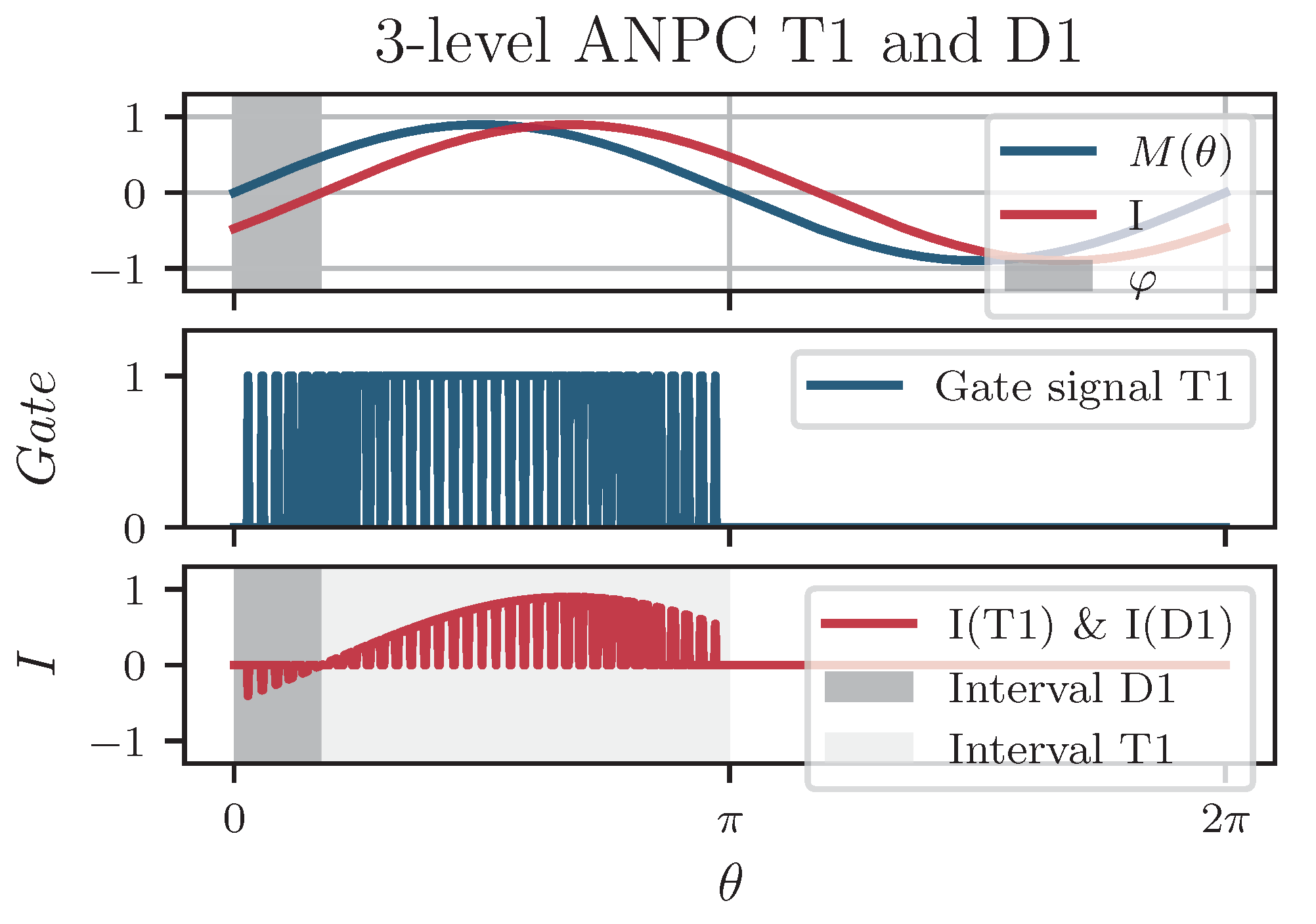
2.2.3. Active Neutral-Point Clamped (ANPC) Converter

The ANPC converter, first proposed by [4], is an extension of the NPC topology where two extra active switches are connected in parallel with the clamping diodes. Using these extra two switches, a more uniform loss distribution among the semiconductors can be achieved while not significantly altering the system efficiency. As for the NPC topology, all switches are subjected to only half the DC link voltage. The increased circuit complexity also becomes evident in the required number of semiconductor devices. The six required transistor–diode pairs in a three-phase two-level VSI stand in contrast to the required 18 in an ANPC topology. Additional gate drive circuits are needed. Using these extra two switches, the neutral state current flow can be actively controlled since two current paths for the neutral state exist, leading to a more uniform loss distribution. In addition to a better loss distribution between semiconductor devices, the redundant switching states can be used to balance the voltages of the DC link capacitors, tackling the DC link voltage unbalance, which occurs periodically in three-level topologies. The upper neutral path is formed by switches T5 and T2 (and their antiparallel diodes), and the lower one is formed by T6 and T3 (and their antiparallel diodes). A better power loss distribution can be achieved by careful selection of the current paths [20,27,38]. This added degree of freedom offers the possibility of multiple modulation schemes to generate the gate signals of an ANPC inverter. Four typical modulation schemes will be discussed in Section 3.2.
In summary, despite the increased circuit complexity and the number of required semiconductors, the three-level topologies described have significant advantages. Depending on the three-level topology, they do not stress the individual switches with the full DC link voltage and are, therefore, a viable option to increase the DC link voltage without having to increase the voltage requirements for the individual switches. Through the increased number of switching positions, losses are distributed over many semiconductors, which provides extended degrees of freedom in converter operation and thermal design. For some topologies, the flexibility offered by the increased number of switch positions and resulting multiple redundant commutation paths results in improved post-fault performance. Furthermore, compared to the standard two-level inverter topology, multi-level inverters incorporate intrinsically lower EMI noise emissions at the inverter output since the waveform approximates the desired sinusoidal shape better [27]. This is beneficial in applications with stringent noise emission regulations but also helps to reduce the size of passive filter components and shift losses away from the already heavily stressed electrical machines.
As mentioned, there exist a variety of possibilities to control the switches applied in the described topologies. With an increasing level number and circuit complexity, more such possibilities result. In the following Section 3, the modulation methods to generate the switches’ gate signals are discussed. A special emphasis is placed on the extended degrees of freedom and, therefore, the capabilities offered by the ANPC topology.

3. Modulation

3.1. Modulation Schemes

The modulation method generates the gate signals for the inverters’ switching elements. Common modulation methods are carrier-based methods, space-vector-based pulse width modulation (PWM) methods, and selective harmonic elimination schemes [11].
Space vector modulation (SVM) represents the state-of-the-art method to control the power transistors of an inverter. In this method, the concept of space vectors is used. These represent discrete voltage vectors, to which appropriate dwell times are assigned. This method generates low harmonic distortion at the inverter output. The RMS fundamental line-to-line voltage utilization ratio of 70.7 % of the DC link voltage in the linear modulation range is larger than for the subsequently described simple carrier-based modulation.
A well-known carrier-based modulation method is the so-called sinusoidal width pulse modulation (SPWM). For a two-level voltage source inverter, the control pulses are generated by comparing a low-frequency sinusoidal reference signal, or modulating wave (which represents the desired line-to-neutral voltage at fundamental frequency), to a high-frequency triangular carrier signal. The ratio of the amplitudes of these two signals to each other is known as the (amplitude) modulation index m a or simply m. The ratio of the two signals’ period times is called the frequency modulation index m f . Generally, the frequency of the carrier wave is a large multiple of the frequency of the modulating wave [39], resulting in so-called synchronous PWM [11]. A drawback of this simple modulation method is the poorer voltage utilization, with a utilization ratio of 61.2 % of the DC link voltage in the linear modulation range. Compared to SVM, this is lower by a factor of 0.865 . Furthermore, this method generates more harmonic distortion in the output currents. Especially as the modulation index increases, SPWM’s performance in terms of harmonic distortion rapidly degrades.
This drawback can be overcome by inserting a so-called zero-sequence signal v 0 , or common mode offset (CMO), into the modulating signal. Through the insertion of such an offset, the output current THD can be reduced and the linearity range of the output voltage can be increased [40]. One example of this is the third harmonic injection (THI) PWM. Here, the third harmonic of the fundamental wave is used as the zero-sequence signal (see Figure 4 and Equation (1)). Similarly, SVM can be implemented by carrier-based PWM [39] through the insertion of a zero-sequence signal (SVPWM). In this case, the CMO consists of the minimum and maximum instantaneous values of the three 120° phase-shifted sinusoidal modulating waves [24] (Figure 4). The zero-sequence signals to be injected in order to obtain the waveforms pictured in Figure 4 can be found in (1). The insertion of such a (time) continuous signal leads to so-called continuous PWM (CPWM). Discontinuous PWM (DPWM) results when discontinuous modulation waves are used to further increase the voltage linearity range and reduce switching losses [40].
v 0 , S P W M = 0 v 0 , T H I P W M = + 1 6 sin ( 3 θ ) v 0 , S V P W M = max ( u a , u b , u c ) + min ( u a , u b , u c ) 2
An advantage of this carrier-based modulation is that it can be easily adapted to multi-level topologies. Multi-level inverter-adapted SPWM is achieved by using offset carrier signals (multi-carrier PWM) to compare to a modulating wave and thus generate the control pulses. In a three-level topology, two (triangular) carriers are needed. There are several options to rearrange these two carrier signals in relation to each other. Examples are the phase disposition (PD), phase shift (PS), phase opposition disposition (POD), or alternative phase opposition disposition (APOD) methods. More information on multi-level inverter multi-carrier PWM techniques can be found, for instance, in [36,40,41]. Examples of PD, PS, and POD carrier signals (three-level case) are shown in Figure 5.
In the following Section 3.2, a more detailed review of the modulation of the gate signals for a three-level ANPC topology will be given. The focus will not be on evaluating the resulting differences in the application of the different carriers—for instance, in terms of the THD and line voltage, which vary slightly [36]. Instead, the different switching frequencies of the switches at different intervals of the fundamental period in the different modulation schemes, as well as their complementary switching behavior, shall be emphasized and visualized (see Figure 6) In order to do so, PD-PWM will be used since no additional overlap or shift in phase angles has to be considered, and the carrier signals are simply placed above and below the zero reference. However, e.g., POD could have been used to emphasize these points equally well.

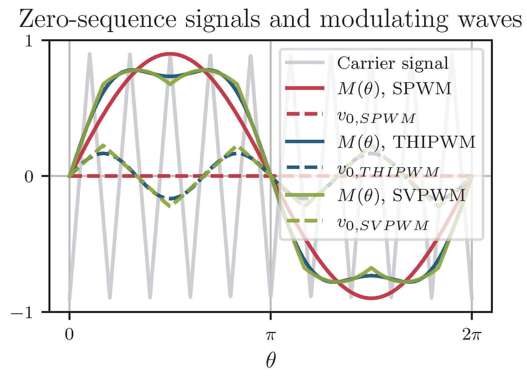
3.2. Three-Phase Three-Level (A)NPC Modulation

In this section, the generation of the gate signals for the NPC and ANPC topology is discussed. As described in Section 3.1, with an ANPC converter, in contrast to a two-level topology, there are extended possibilities for shifting between switching states. The main difference between the modulation schemes is the neutral current path to output the zero state. The modulation schemes intentionally configure this neutral current path while not affecting each leg’s output voltage. This neutral current path enables a greater number of voltage levels in the output compared to traditional two-level inverters, which reduces the harmonic content and improves the output quality, making the ANPC topology suitable for applications where high-quality output voltage waveforms are required. The flexibility offered by the increased number of switch positions and multiple redundant commutation paths results in improved post-fault performance. ‘Limp home’ operational mode can be implemented, and the inverter can continue to operate at reduced power [42,43]. This is essential for safety-critical application areas such as aviation. The extended degrees of freedom make the implementation of novel modulation algorithms possible, which helps to optimize the loss distribution and EMI performance. Optimizing the distribution of losses allows for the equalization of the junction temperatures, which improves the reliability and benefits the cooling system. Furthermore, the extended degrees of freedom in ANPC inverters enable better voltage balancing among the switching devices and within the DC link.
Four typical modulation schemes for the ANPC topology will be discussed [21,22,24,25]. Figure 6 gives an overview of the different modulation strategies and resulting switching patterns for each switching position in the ANPC topology. As mentioned in the previous Section 3.1, a zero-sequence signal can be injected into the modulating sine wave to alter the output voltage. This approach is also applicable here but is not shown or described for simplicity reasons. It will be addressed again later in the course of this work.

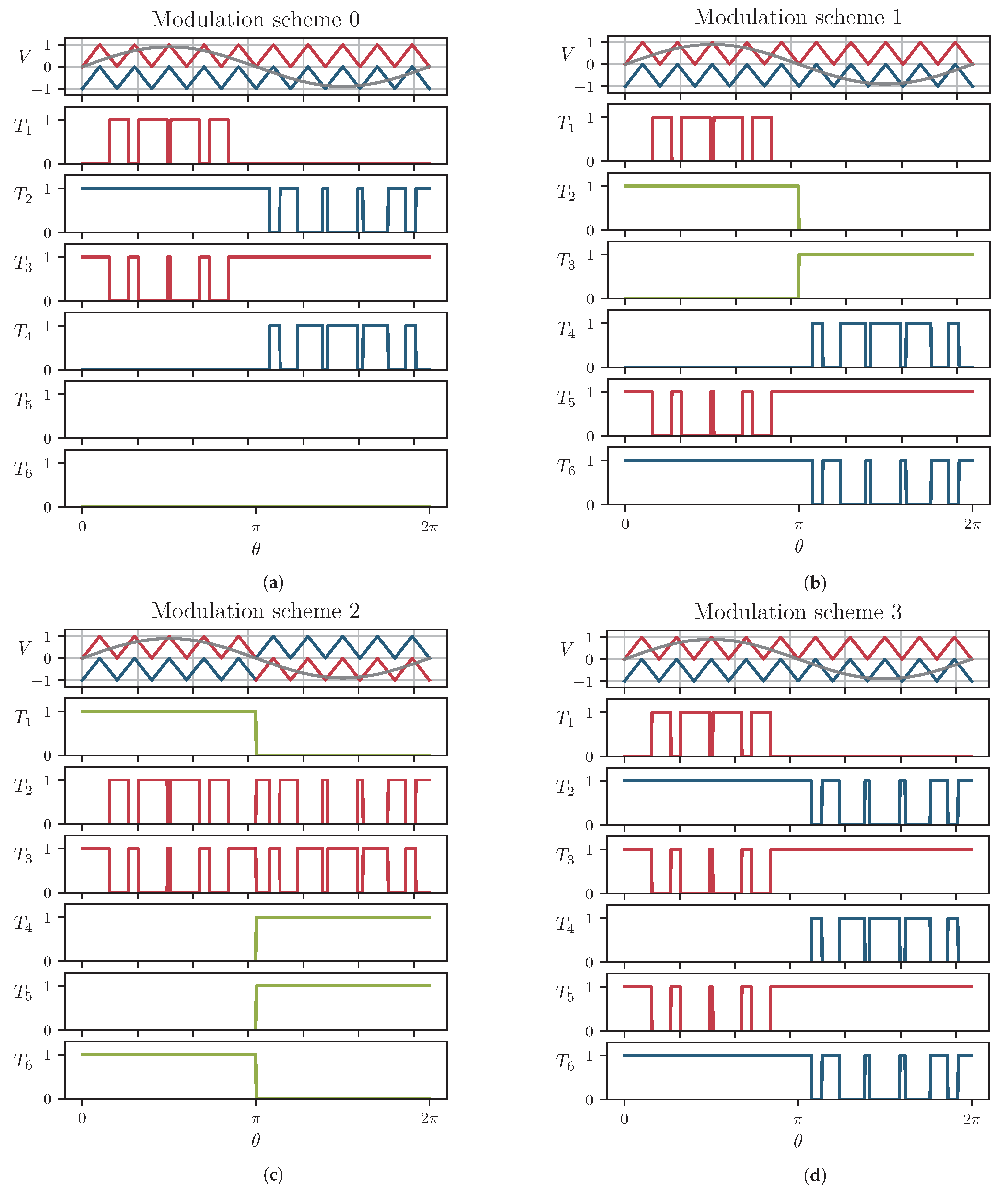
3.2.1. ANPC Modulation Scheme 0

As with the three-level TNPC topology, where an equivalent to the standard two-level VSI is achieved by permanently turning off the bidirectional switch, the ANPC topology can also be operated in an NPC manner. Therefore, this modulation scheme practically equals the NPC modulation. Modulation scheme 0 constantly keeps the switches T5 and T6 off, making only their anti-parallel diodes available for midpoint clamping. The switching pattern for this modulation scheme is shown in Figure 6a. In this case, the gate signals are generated by a modulating sine wave and two triangular carrier signals in PD-PWM. The upper carrier is used to switch on T1 and T3 complementarily over half the line cycle, while the lower carrier is responsible for generating the control signals for T2 and T4 over the other half of the fundamental period. While T1 and T3 operate at f s w , T2 and T4 are kept on and off, respectively. As mentioned, the transistors T5 and T6 are switched off over the whole fundamental period [24,25].

3.2.2. ANPC Modulation Scheme 1

In this scheme, only T1 and T4, as well as T5 and T6, are modulated at the switching frequency and in a complementary manner over half the fundamental period, while remaining in a constant state over the other half. The inner switches T2 and T3 are turned on during the entire positive or negative half cycle of the current, respectively. While not being operated at a high switching frequency, switches T1 and T4 are constantly kept off, and switches T5 and T6 are constantly kept on [22,24,25]. The resulting gate signals for this scheme are given in Figure 6b. The switching losses in the slow-switching inner switches are expected to be low and the conduction losses in these switches are not dependent on the modulation index [22]. This makes a hybrid construction using different semiconductor material switch types feasible. The inner switches T2 and T3 could be realized by Si IGBTs, with excellent conduction but poor switching characteristics, therefore allowing for a cost reduction considering the good availability of Si IGBTs. The outer switches could be realized with SiC MOSFETs. In this modulation scheme, the neutral current path is located in the upper cell for the positive half cycle (top cell commutation) and the lower cell for the negative half cycle (bottom cell commutation), resulting in so-called ‘same-side clamping’. Making use of only these short, low-stray-inductance commutation paths results in the good suitability of this modulation scheme for a setup where each cell is implemented by a half-bridge module [21]. For more details on the application aspects, refer to Section 5.

3.2.3. ANPC Modulation Scheme 2

In contrast to the previous modulation scheme 1, in modulation scheme 2, there is only one high-frequency switch pair (T2 and T3), but four switches operate at the fundamental frequency (T1 and T4, T5, and T6) [21]. This modulation scheme again allows for the possibility of using higher-performance components only for inner switches T2 and T3, where high switching losses are expected. Here, the complementary switch pair T2 and T3 is modulated by the upper carrier for the positive and by the lower carrier for the negative half cycle [24,25] (see Figure 6c). T1 and T6 are kept off for the negative half cycle. T4 and T5 are kept off for the positive half cycle. This scheme uses only long commutation paths (‘opposite-side clamping’), which accentuates parasitic elements in this longer commutation circuit and makes the use of integrated and optimized three-level power modules advisable.

3.2.4. ANPC Modulation Scheme 3

In modulation scheme 3, we alternate between the fundamental and switching frequency [22]. T3 and T5 are switched simultaneously and are operated complementarily to T1. The gate signals of these switches are generated using the upper carrier wave. T4 is switched complementarily to the switches T2 and T6, the latter of which are turned on and off simultaneously. The lower carrier wave is used. In this scheme, the upper and lower neutral current paths are used together, which yields the name ‘full-path clamping’ [24,25]. The two parallel current paths reduce the conduction loss during the neutral state and allow for more uniform switch utilization. The trade-off is higher switching loss. This scheme is well suited for the use of SiC MOSFETs, not only due to their good switching performance but also their higher R D S ( o n ) positive temperature coefficient, resulting in excellent current sharing capabilities [44].
While the various ANPC modulation schemes, as discussed, do not alter the output voltage waveforms of the individual phase legs, a more uniform loss distribution can be achieved. Analytical models can be used to predict the losses and their distribution over the different switch positions, not only for the ANPC but also for the other discussed topologies.

4. Analytical Power Loss Modeling

Power losses consist of a number of individual loss components. While components such as driving as well as blocking losses are usually neglected, the static on-state (conduction) losses and the switching losses (turn-on, turn-off, reverse recovery losses) mainly determine the expected power dissipation in the switching component [8]. Various methods exist for the prediction of losses in power semiconductors. One possibility is the complete numerical simulation of the circuit. This allows detailed information to be obtained not only in terms of efficiency but also, for example, to investigate the influence of parasitic elements. For basic investigations, however, in order to gain a general understanding, and to compare different inverter topologies, analytical calculations are beneficial [19,22]. This allows us to identify the dependencies of the losses on different device parameters (e.g., conduction and switching characteristics), operating conditions (e.g., current, voltage, power factor), topologies, and modulation schemes. In the following subsections, first, the analytical calculation of the conduction losses is reviewed. Subsequently, the approach for the switching losses is described.
Some simplifying assumptions have to be made when formulating the analytical loss equations. Simplifications made are as follows.
  • The constant switching frequency is assumed to be large in comparison to the fundamental frequency ( f s w > > f o u t ).
  • For the phase current, a sinusoidal waveform is assumed, not considering current ripple.
  • Dead times or transistor and diode switching times are not taken into account. This may lead to a systematic underestimation of the total losses.
  • There are limitations for reverse conducting power devices such as MOSFETs: current sharing between parallel paths is not taken into account.
In the first step, as for the description of the modulation schemes, sine-triangle PWM (SPWM) will be used to simplify the analysis. The literature suggests SPWM as a good approximation for the power loss calculation [19]. However, with the later presented calculation approach, it will be possible to investigate other continuous PWM schemes.

4.1. Conduction Losses

The calculation of the conduction losses is based on a simple analytical description of the operating point and subsequent integration of the loss formulas over a fundamental period [45]. For the steady state of the circuit, the conduction losses of a power semiconductor can be calculated using the following universal equation.
P c o n d = 1 2 π θ 1 θ 2 i ( θ ) · v ( θ ) d θ
v ( θ ) is the voltage over the component for a given current flow i ( θ ) . For a (bipolar) IGBT, i ( θ ) equals the collector current i C ( θ ) and v ( θ ) is the collector–emitter voltage v C E ( θ ) . For a (unipolar) MOSFET, i ( θ ) and v ( θ ) would be the drain current i D ( θ ) and the drain–source voltage v D S ( θ ) , respectively. θ is the electrical angle, and θ 1 and θ 2 are the integration limits or conduction intervals.
Conventionally, an IGBT’s output characteristic is approximated using an on-state slope resistance r C E and the collector–emitter threshold voltage V C E 0 (see Figure 7). For MOSFETs, the drain–source turn-on resistance R D S ( o n ) and no knee voltage have to be considered. For a more consistent description, r 0 and V 0 will be used in the following, resulting in a linearized output characteristic: v ( θ ) = V 0 + r 0 · i ( θ ) .
The (linearized) output characteristic in combination with the modulation function M ( θ ) , a term that takes into account the switching states, represents a well-known approach to the calculation of the on-state power loss [22,45,46].
P c o n d = 1 2 π θ 1 θ 2 i ( θ ) · ( V 0 + r 0 i ( θ ) ) · M ( θ ) d θ = 1 2 π θ 1 θ 2 ( V 0 i ( θ ) + r 0 i ( θ ) 2 ) · M ( θ ) d θ = V 0 I a v g + r 0 I r m s 2
M ( θ ) is a continuous function in the range of 0 to 1, which replaces the discrete-time switching function τ ( θ ) in the shift to infinitesimally small switching periods. The modulation function is dependent on the power factor cos ( φ ) and the modulation index or modulation factor m. The power factor accounts for the phase shift φ between the fundamental components of the inverter output voltage and phase current. For an energy flow from the DC to the AC side, i.e., for inverter operation, cos ( φ ) > 0 applies. The modulation index is referenced to the virtual neutral point of the load (phase-neutral) and the (virtual) midpoint of the DC link voltage [8]. m is defined as the ratio of the fundamental amplitude of the phase-neutral AC voltage to half the DC link voltage.
m = V ^ p h a s e V D C 2
The modulation function M ( θ ) and the integration limits θ 1 and θ 2 vary for different topologies and modulation schemes. The terms to be applied in the corresponding case are shown in Table 2 and Table 3 [9,21,22]. However, when applying the modulation functions given in this table, it should be considered that different combinations of modulating functions and conduction intervals can lead to the correct loss equation and subsequent integration. As an example of this, position D1 in the NPC topology can be named. Here, the integration interval ( π , π + φ ) in combination with the modulating function m · sin ( θ ) would lead to exactly the same result if the opposite sign of current is considered in the following integration.
Moreover, it is important that in one given loss formula, due to the loss symmetry of the upper and lower half of each phase leg, always two devices are described.
To illustrate the procedure, first, the determination of the analytical conduction loss formula for the switch position T1 (and T4) of a standard two-level VSI will be described. This is followed by a detailed review of the derivation of the loss formulas of T1 and D1 in ANPC modulation scheme 1. Current waveforms and corresponding modulation functions for the other discussed ANPC modulation schemes are given in Figure 8 [21,24,25].
For the switches T1 and T4 of a standard two-level VSI, the modulation function ( 1 + m · sin ( θ ) ) / 2 will be used. Substituting this modulation function (see Table 3), as well as the phase current i ( θ ) = I ^ sin ( θ ) (sinusoidal phase current assumed; see previously listed simplifications), into (3) yields
P c o n d , T 1 = 1 2 π φ π + φ ( V 0 I ^ sin ( θ φ ) + r 0 ( I ^ sin ( θ φ ) ) 2 ) · 1 + m · sin ( θ ) 2 d θ = 1 2 π 0 π ( V 0 I ^ sin ( θ ) + r 0 ( I ^ sin ( θ ) ) 2 ) · 1 + m · sin ( θ + φ ) 2 d θ
Solving this integral results in the analytical formula for the calculation of the conduction losses (cf. Appendix A Table A1):
P c o n d , T 1 = V 0 · I ^ ( 1 2 π + m cos φ 8 ) + r 0 · I ^ 2 ( 1 8 + m cos φ 3 π ) = 1 24 π V 0 I ^ · 3 4 + m π cos ( φ ) + r 0 I ^ 2 · 3 π + 8 m cos ( φ )
Figure 9 shows the phase current, modulating signal, phase angle, as well as conduction and switching loss intervals for D1 and T1 of a three-level ANPC topology in modulation scheme 1. One can see that T1 conducts a positive (forward) current not over the full AC line cycle of length 2 π , but only over half of this period. As previously, substituting the correct modulation function (Table 3), as well as a sinusoidal phase current into (3), yields
P c o n d , T 1 = 1 2 π θ 1 θ 2 ( V 0 i ( θ ) + r 0 i ( θ ) 2 ) · M ( θ ) d θ = 1 2 π φ π ( V 0 I ^ sin ( θ φ ) + r 0 ( I ^ sin ( θ φ ) ) 2 ) · m · sin ( θ ) d θ = 1 2 π 0 π φ ( V 0 I ^ sin ( θ ) + r 0 ( I ^ sin ( θ ) ) 2 ) · m · sin ( θ + φ ) d θ = m 12 π V 0 I ^ 3 ( π φ ) cos ( φ ) + sin ( φ ) + r 0 I ^ 2 2 ( 1 + cos ( φ ) ) 2
Note that the equation greatly simplifies when unipolar devices are considered since the term associated with V 0 does not have to be considered.
For the diode D1 in ANPC modulation scheme 1, the modulation function and integration limits can also be derived from Table 3 or Figure 9 as follows:
P c o n d , D 1 = 1 2 π 0 φ ( V 0 ( I ^ ) sin ( θ φ ) + r 0 ( ( I ^ ) sin ( θ φ ) ) 2 ) · m · sin ( θ ) d θ = m 12 π ( V 0 I ^ 3 φ cos ( φ ) + sin ( φ ) + r 0 I ^ 2 2 ( 1 cos ( φ ) ) )
Note the negative sign of the current in (8), due to the prevailing negative phase current during the conduction interval of the diode.
It can be observed that this approach quickly results in complex equations, which can take many different forms and can therefore only be compared between different literature sources with great effort [20,21,22,23,24]. Furthermore, for every entry in Table 2 and Table 3, one such equation is required. Although switches as well as diodes in the upper and lower half of a phase leg are stressed equally due to the prevailing symmetry, still a great number of equations is necessary to describe every topology and modulation scheme. For example, the previously discussed ANPC modulation scheme 1 needs a total of six such equations. For the other ANPC modulation schemes, even more integrations are required, since, for one device, more than one modulation function and integration interval apply. The full set of loss equations can be found in Appendix A (Table A1). Note that these equations are only valid for SPWM. Moreover, note that the equations simplify when unipolar devices such as SiC MOSFETs are used, since only the term associated with I r m s 2 has to be considered in the integration.
As mentioned earlier, this approach can be extended to other modulation strategies, such as SVPWM or THIPWM, by inserting a zero-sequence waveform into the modulation signal (Figure 4). See an example in [19], where this approach for two-level VSI is extended to SVPWM by using a modified modulation factor, which is a composition of sine functions expressed as a Fourier series. In this case, the term m · sin ( θ ) in the modulation function ( 1 + m · sin ( θ ) ) / 2 will be replaced by the following expression:
m · sin ( θ ) + 3 3 8 π k = 0 ( sin ( 3 · ( 4 k + 1 ) · θ ) 18 k 2 + 9 k + 1 sin ( 3 ( 4 k + 3 ) · θ ) 18 k 2 + 27 k + 10 )
This modulation function can then be used in the integration, cf. (5), which results in [19]
P c o n d , T 1 = V 0 · I ^ ( 1 2 π + m cos φ 8 ) + r 0 · I ^ 2 ( 1 8 + m · ( cos φ 3 π + F S V P W M 2 π ) )
While, for the previously discussed SPWM, F S V P W M would be zero, for SVPWM, the following term has to be used:
F S V P W M = 6 3 π ν cos ( k · φ ) k 5 5 k 5 + 4 k cos ( l · φ ) l 5 5 l 3 + 4 l for l = 3 ( 4 ν + 1 ) ; k = 3 ( 4 ν + 3 ) ; ν = 0 , 1 , 2 ,
It becomes apparent that extending the loss equations to other modulation strategies further adds to the complexity and is therefore usually avoided in the literature [24]. This holds especially true for topologies and modulation schemes requiring a greater number of integrations. This is why the extension to SVPWM for, e.g., the ANPC topology will not be discussed in this work. Implementing these equations in a simulation script is prone to human error and should therefore be avoided. Instead, this paper proposes to compute the definite integrals using numerical integration methods already incorporated in state-of the art programming languages such as Python or MATLAB. For more details, see Appendix A and Appendix B.

4.2. Switching Losses

While the conduction losses are mainly determined by the flowing current, the switching losses depend proportionally on the switching frequency f s w . Therefore, the switching losses are obtained by multiplying f s w with the switching energy loss E s w . The same applies to the diodes, where, instead of the turn-on and turn-off energy loss ( E o n and E o f f ), the reverse recovery energy E r r is considered [8].
P s w , T = f s w · E s w = f s w · ( E o n + E o f f ) P s w , D = f s w · E r r
Manufacturers’ datasheets specify the switching energy losses in dependency on a certain (nominal) current and voltage, as well as a temperature [8]. Oftentimes, a particular d i / d t is also defined. Adaptation to the real application can, in the simplest case, be done by linear interpolation of the given values, as shown in (13) [8,22,45,46].
E o n ( i , v ) = E o n , n o m ( I n o m , V n o m ) · ( i I n o m ) k i , T · ( v V n o m ) k v , T E o f f ( i , v ) = E o f f , n o m ( I n o m , V n o m ) · ( i I n o m ) k i , T · ( v V n o m ) k v , T E r r ( i , v ) = E r r , n o m ( I n o m , V n o m ) · ( i I n o m ) k i , D · ( v V n o m ) k v , D
However, it becomes evident from the switching energy curves in the manufacturers’ datasheets that these energies are not linearly dependent on the current and voltage. Therefore, various possibilities exist to better approximate the energy loss value for a given device. One approach is the introduction of exponents for the linear scaling terms (see (13)). For Si IGBTs, ref. [8] suggests the use of k v , T 1.3 1.4 for the voltage scaling term while keeping the linear interpolation over the current. For Si diodes, no linear dependency for the loss energy over the current can be assumed. k v , D 0.6 and k i , D 0.6 are stated for the diodes. Other sources such as [46] suggest the use of a term ( 0.45 · i I n o m + 0.55 ) instead of the linear current scaling, while linearly interpolating over the voltage. However, caution is advised when using these extensions since they may have to be taken into account in the subsequent transition to the average current value and complicate the integral to be solved. In this publication, these exponents are set equal to 1 to preserve the generality of the results. A temperature coefficient [8] can be used to account for the switching energy loss temperature dependency.
In addition to the (improved) linear interpolations, the second basic principle for the present analytical switching loss calculation is the assumption that the switching losses during a half-wave of the sinusoidal current are equal to the switching losses for an equivalent direct current, which is the average value of the respective current [8,46].
To calculate the switching losses, the switching energies are integrated over a half-wave and multiplied with the switching frequency. In the following, two examples of this integration will be given—one for the conventional two-level VSI, and one for T1 (T4) and D1 (D4) in the previously discussed ANPC topology in modulation scheme 1 (see Figure 9).
For the two-level topology, the full DC link voltage is switched and is therefore used as v. The (phase-shifted) current is assumed to be sinusoidal: i = I ^ · sin ( θ φ ) . The switching angles or integration limits are ( φ , π + φ )
P s w , T 1 = f s w · 1 2 π θ 1 θ 2 E s w · i I n o m · v V n o m d θ = f s w · 1 2 π φ π + φ E s w · I ^ · sin ( θ φ ) I n o m · V D C V n o m d θ = f s w · 1 2 π 0 π E s w · I ^ · sin ( θ ) I n o m · V D C V n o m d θ = f s w · 1 π · E s w · I ^ I n o m · V D C V n o m
For three-level topologies, half the DC voltage has to be used as v. Furthermore, different switching loss intervals have to be considered. For an ANPC topology, the integration limits for T1 would be ( φ , π ) (see Figure 9 and Table 4), resulting in the following expression for the switching losses:
P s w , T 1 = f s w · 1 2 π φ π E s w · I ^ · sin ( θ φ ) I n o m · V D C 2 V n o m d θ = f s w · 1 + cos ( φ ) 2 π · E s w · I ^ I n o m · V D C 2 V n o m
However, it should be noted that for some elements, the negative sign of the current has to be considered in this integration. An example of this would be D1 in the previous topology with the switching loss interval ( 0 , φ ) :
P s w , D 1 = f s w · 1 2 π 0 φ E r r · I ^ · sin ( θ φ ) I n o m · V D C 2 V n o m d θ = f s w · 1 cos ( φ ) 2 π · E r r · I ^ I n o m · V D C 2 V n o m
An overview of the switching loss intervals, as well as the resulting factors for the switching loss calculation, is given in Table 4. Note that these, as for the modulation functions in Table 2 and Table 3, are valid only for SPWM. The factors in Table 4 only apply to pure linear scaling of the switching energies.
Here, too, an approach that avoids manual integration, as presented in Section 4.1, could be used. However, since less complex equations result from the integration, this might not be as beneficial. Further, note that the switching losses of switches switching with output frequency are not considered here and thus are set to zero. This simplification is possible because the output frequency is much smaller than the switching frequency. This approach only applies to continuous PWM [19]. To assess losses in DPWM techniques, a so-called switching loss factor (SLF) could be used [47].
In the following section, the design, packaging, and thermal aspects for the realization of such (multi-level) inverters will be discussed. Using the approach described in this section, power loss analysis is performed for different topologies, device configurations, and modulation schemes.

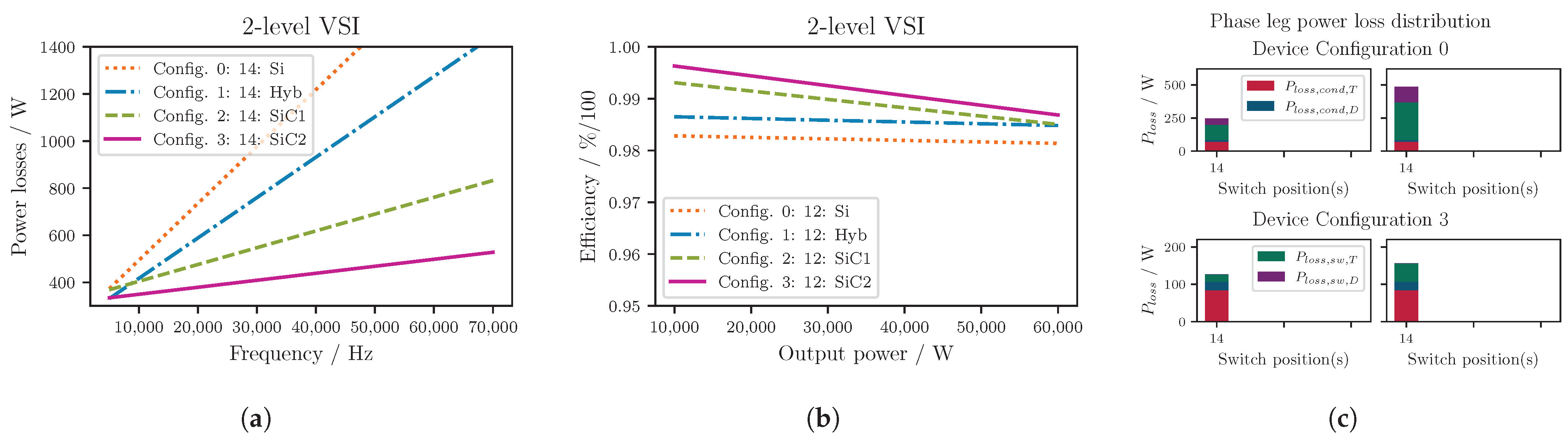
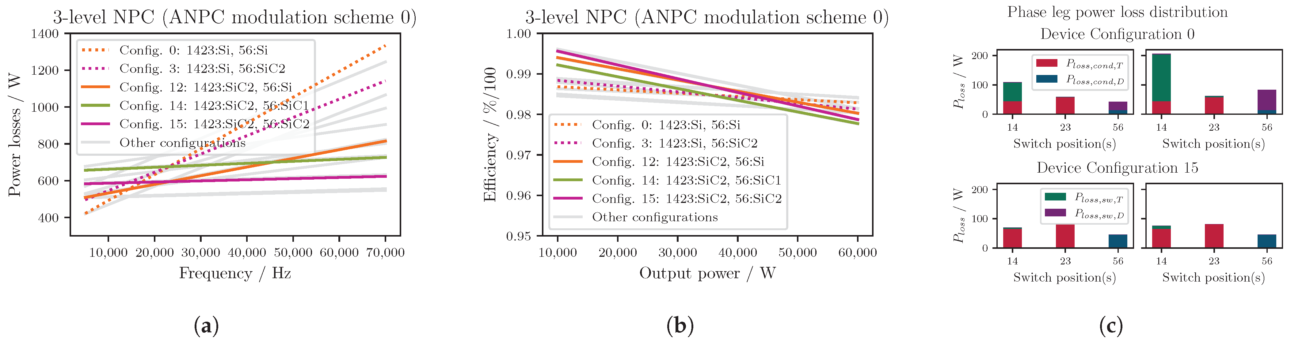
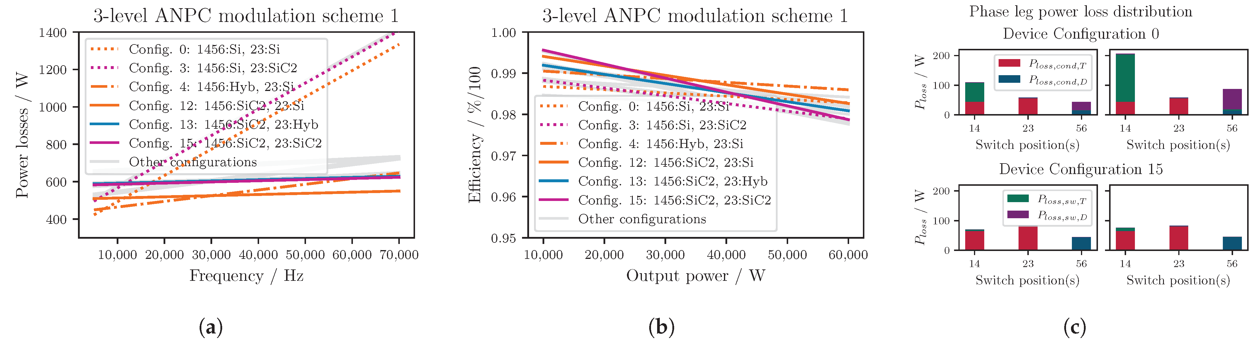
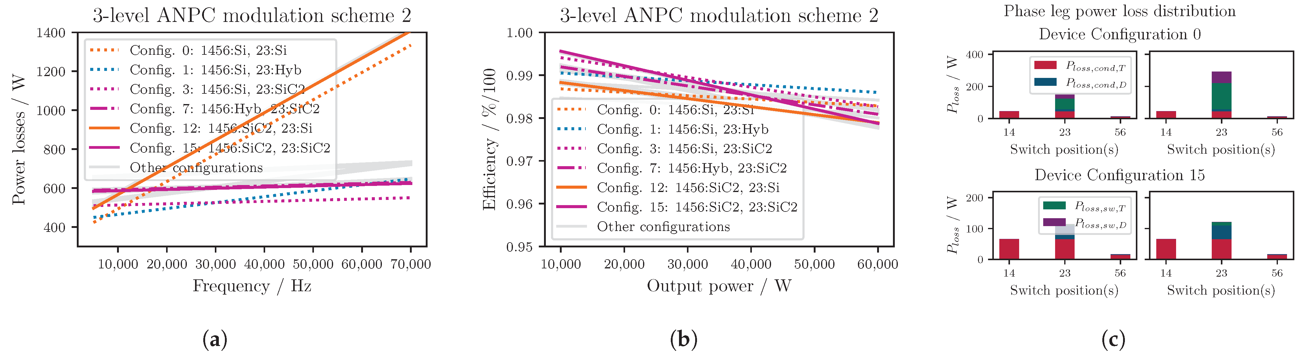
5. Application Aspects and Results

5.1. Design, Packaging, and Thermal Aspects

For the realization of inverters in general and multi-level inverters in particular, several packaging forms of power semiconductors exist. They range from single switches, such as the typical TO-247 or a surface mount package, to packages with all transistors and diodes fully integrated into one module. For a standard two-level VSI, this would be a full-bridge or so-called ‘six pack’ package. Often, a single-phase leg is integrated into one package. Half-bridge modules are common, also due to the widespread use of the B6 topology. Moreover, modules with integrated peripheries exist, which could include (gate) driving, protective units, or (current) measurement circuits (so-called intelligent power modules, IPM). However, it should be noted that the universality of these power modules is reduced with the increasing integration level [8].
In the industrial drive and automotive EV sector, the use of power modules with multiple power semiconductors in one package is common. These power module integration capabilities offer more simplicity in design, higher reliability, and, as they provide better heat spreading properties, higher output power and power density in direct comparison to discrete switches [48]. However, when the application of WBG devices or a hybrid device configuration is desired, the availability of such modules is limited, especially for configurations with more than two levels. Other solutions, such as discrete switches, have to be applied. In order to further decrease EMC/EMI issues, the system footprint, and the integration effort—and to increase the overall power density—multi-level power modules will be necessary in the future. Besides the parasitic elements, thermal aspects are also challenging. The power loss model represents the interface between electrical and thermal considerations. The equations can be used to evaluate the junction temperatures of discrete components. Especially for power modules employing a larger number of semiconductor chips on a common base plate, the thermal behavior and heat spread within this module must be examined in more detail. In terms of temperature distribution, for example, a high-loss Si device could limit the junction temperature of a SiC device in one power module. The study [49] gives a good impression of the challenges faced when designing such power modules with particular respect to the mandatory low-inductive design. An exemplary implementation of an ANPC inverter with a hybrid switch configuration in an ‘Easy3B’ package is given in [26]. Another such three-level ANPC module available would be the Infineon F3L11MR12W2M1_B74 EasyPACK™ module [50]. Here, too, a hybrid configuration using different semiconductor materials is used. This power module utilizes SiC MOSFETs as inner switches while keeping Si IGBTs on the outer and midpoint switch positions [22]. However, it should be noted that due to the diverse modulation strategies, especially for the ANPC topology, a variety of optimized solutions are conceivable in terms of the types of power semiconductors and module layouts. For example, ref. [18] uses GaN HEMTs for positions T2 and T3 since they can achieve high switching frequencies due to their low output capacitances. The challenge of the limited current carrying capability of state-of-the-art GaN switches is overcome by interleaving respective switches. Besides the use of discrete power devices or dedicated three-level modules, the construction of such multi-level topologies from two-level modules is possible. In practice, however, this approach leads to very long conduction paths and commutations across module boundaries. Especially for the opposite-side clamping used in ANPC modulation scheme 2 (see Section 3.2), these long commutation paths have a negative effect. Stray inductance caused by the long commutation paths leads to voltage overshoots, so part of the advantage over two-level designs can be lost [35]. Ref. [35] provides a good overview of the advantages and drawbacks and discusses how to set up three-level configurations from two-level half-bridge modules.
In addition to the setup of multi-level inverters from different power semiconductor packaging technologies, the design of the inverter itself and the thermal management—for instance, under the consideration of cryogenic cooling [51]—are crucial. For multi-level inverters with their increased number of switch positions and offered degrees of freedom in terms of current paths, the optimization of the commutation loop is one of the primary challenges. Sources of inductance here are the commutation loop stray inductance, the semiconductor device self-inductance, and the DC link capacitor self-inductance, which all should be optimized to improve efficiency and mitigate voltage overshoots. Besides their self-inductance, the DC link capacitors also play a crucial role in inverters and have, therefore, to be optimized [52]—for instance, to achieve high power density requirements. The design and optimization of the cooling system for a multi-level inverter has to be carried out. For multi-level topologies, consideration of the type of cooling and the number of switches per heat sink is relevant. The use of WBG semiconductors, which are capable of higher-temperature operation, in combination with the mentioned higher-level topologies, incorporating a larger number of switches and therefore improved loss distribution, place forced [15] and even natural convection [53] air cooling into the focus for aircraft power electronics. Additive manufacturing technologies and optimization algorithms have recently been used to fabricate more complex structured heat sinks [54]. This allows cooling performance and weight to be improved simultaneously. Furthermore, innovative materials and the combination of different materials within a heat sink structure are also feasible to achieve lighter and more efficient heat sinks [55]. Applying such sophisticated heat sink structures is quite realistic, as seen in the example of the Siemens SD104 aircraft inverter, which has already been operated onboard the Magnus eFusion electric test plane. It utilizes silicon-carbide semiconductors and incorporates a micro-channel cooling plate [56].

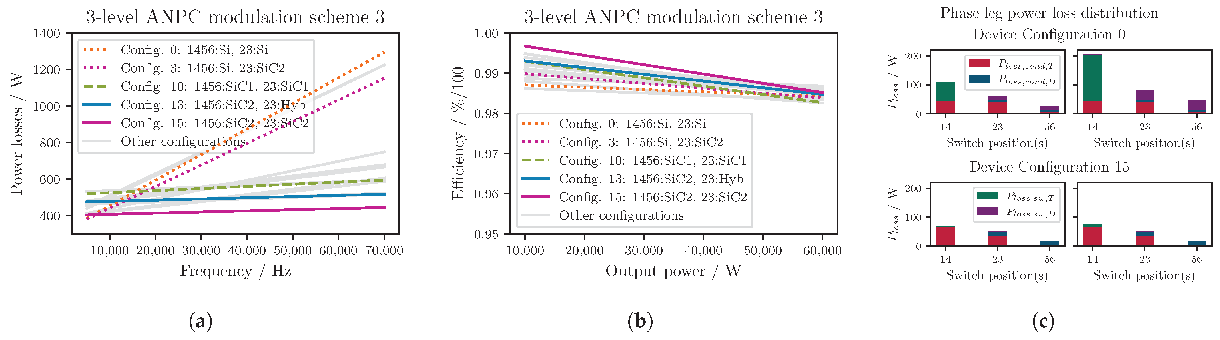
5.2. Exemplary Power Loss Analysis

In the literature, often, fictive module configurations are assumed. These are based on the data of semiconductors, which are used in, e.g., half-bridge modules. This allows for an analysis of a large number of configurations in the desired power range despite the limited number of three-level modules currently available on the market. However, this approach lacks practicality in that it will not be possible to actually use and test such configurations easily in practice. For this reason, a different approach is taken in this work. To show the effects of different (hybrid) switch configurations, the overall system is scaled down so that discrete devices in the TO-247 package can be utilized for every switching position. In this scaled down system, no paralleling of devices has to be considered.
In the following, a power loss analysis will be performed and discussed for different topologies, modulation schemes, and device configurations using the previously described approach. The calculations aim to evaluate which semiconductors will work best in which topology and which PWM scheme would be best suited.
For this study, a three-phase system with a DC link voltage of 800 V is assumed. The output power is varied around a nominal value of 40 kW. With an assumed V r m s , l i n e l i n e of 490 V ( m = 1 ), an approximate nominal phase current of 50 A is present. The power factor is assumed to be cos ( φ ) = 0.95 , and the fundamental frequency is set at 250 Hz. This relatively high output frequency is due to the intended application as an aircraft propeller inverter. Propeller applications tend to be high-torque rather than high-speed, resulting in an increased number of pole pairs. For the switching frequency, a range between 5 kHz and 70 kHz is swept, as shown in the following figures. For the frequency sweep, a fixed inverter output power of 50 kW is set. Thermal considerations must be taken into account. For this section’s power loss calculation, discrete parameters were extracted from the power semiconductor datasheets. The considered semiconductor devices and their associated parameters are shown in Table 5. The device’s non-linear output characteristics are described by first-degree functions (c.f. Equation (3)). A more accurate representation in the form of higher-degree functions would influence the subsequent integration and the complexity of the resulting power loss equations and is therefore omitted here. For the switching energies, the datasheet specifications were scaled linearly over the current and voltage in accordance with common scientific practice (cf. (13)). The parameters required for this are also listed in Table 5. Note that these parameters are temperature-dependent. This dependency could be, depending on the relation of electrical to thermal time constant, introduced into this model by modeling the device parameters as multi-dimensional, temperature-dependent functions or the use of parameter look-up tables. However, in this work, mean-value analysis with temperature considered as a stationary parameter is performed. The plot of losses over switching frequency, as well as efficiency over output power, is limited to the thermally safe region. A maximum device junction temperature T j of 150 °C is assumed for all calculations. The limits of the curves in Figure 10, Figure 11, Figure 12, Figure 13, Figure 14 and Figure 15, where present, indicate the thermal limits of the various topology device configurations at an assumed case temperature of T c = 70 °C. In order to fully explore all possible semiconductor device combinations in the different topologies, all device combinations are considered. For the switches subjected to the full DC link voltage, 1200 V components are employed. Otherwise, 650 V components are used. The figures showing the resulting power losses for different switching frequencies, the efficiencies over the output power, as well as power loss distributions for the different topologies and device combinations are discussed in the following.
Figure 10a shows the resulting power losses for the named operating point over the described switching frequency range for a standard two-level VSI. It can be seen that the inverter consisting of Si components only (configuration 0) performs worse than its counterparts over almost the full switching frequency range. For even lower switching frequencies, however, it is the SiC-MOSFET-based configurations (deemed as SiC1 and SiC2) that are expected to have higher losses. Furthermore, it can be seen that the SiC-based solution, which employs an additional Schottky barrier diode (SBD) (SiC2, configuration 3), has an even flatter dependence on f s w , compared to the solution only utilizing the MOSFET’s body diode (SiC1, configuration 2). This is partly due to the SBD’s negligible reverse recovery losses. Moreover, the on and off switching energies for these two configurations vary, even though the same chip is used as the transistor (see Section 5). This is due to the fact that the switching characteristics of the transistor are influenced to a non-negligible degree by its commutation partner—in this case, the anti-parallel Schottky barrier diode. In contrast to the losses over the frequency, the Si-based solutions have a less pronounced drop in efficiency over the output power than the MOSFET configurations (see Figure 10b). Figure 10c shows the power loss distribution for different device configurations and for two switching frequencies of 20 kHz and 50 kHz, respectively.
Figure 10. Power losses for two-level VSI. (a) Inverter total power losses ( P o u t = 40 kW) and (b) inverter total efficiency ( f s w = 20 kHz), where a number is assigned to each (hybrid) switch configuration (e.g., ‘Config.0’) and the type of switch used for each switching position is stated subsequently (e.g., Si for switch position(s) 1 and 4: ‘14:Si’). For the naming of the configurations, see Table 5. (c) Power loss distribution in one phase leg for different configurations and for frequencies of 20 kHz (left) and 50 kHz (right).
Energies 16 06710 g010
A similar behavior is present for the TNPC topology (Figure 11a). Here, the configurations employing Si IGBTs (e.g., configurations 0 and 3) also have a steeper loss dependency on the switching frequency. The configurations with SiC-MOSFETs perform better for higher switching frequencies. Since the utilized co-packed hybrid switches are highly optimized for higher switching frequencies, even though IGBTs are used, they perform well for higher f s w (see configuration 13 in Figure 11a). Bipolar Si IGBTs typically offer lower conduction losses than unipolar SiC-based switches for a given current, further reducing the losses of these configurations. In configuration 12, it is mainly the switching losses of the diodes in positions 2 and 3 that lead to higher losses at higher switching frequencies, while the switching losses of the transistors in positions 1 and 4 increase only marginally. Compared to the standard two-level VSI, lower total losses prevail.
Figure 11. Power losses for three-level TNPC. (a) Inverter total power losses ( P o u t = 40 kW) and (b) inverter total efficiency ( f s w = 20 kHz), where a number is assigned to each (hybrid) switch configuration (e.g., ‘Config.0’) and the type of switch used for each switching position is stated subsequently (e.g., Si for switch position(s) 1 and 4: ‘14:Si’). For the naming of the configurations, see Table 5. (c) Power loss distribution in one phase leg for different configurations and for frequencies of 20 kHz (left) and 50 kHz (right).
Energies 16 06710 g011
The NPC topologies’ loss behavior is shown in Figure 12a. The losses and loss distribution shown correspond to the ones of an ANPC topology in modulation scheme 0. All Si IGBT-based solutions perform better for lower switching frequencies, but the losses strongly rise for higher f s w . The advantage of using SiC diodes as midpoint clamping diodes becomes evident when comparing configurations 0 and 3 or configurations 12 and 15. While, for configuration 12, the diode switching losses increase drastically for higher f s w , this is not the case for the SiC SBDs, e.g., in configuration 15, as can be seen in Figure 12c. For the latter configuration, the middle switches become the most heated devices. For higher switching frequencies, SiC MOSFETs, preferably with an additional SBD, should be used with regard to the expected power dissipation. It should be noted, however, that their efficiency decreases more sharply at higher output powers (see Figure 12b).
Figure 12. Power losses for three-level NPC or ANPC in modulation scheme 0. (a) Inverter total power losses ( P o u t = 40 kW) and (b) inverter total efficiency ( f s w = 20 kHz), where a number is assigned to each (hybrid) switch configuration (e.g., ‘Config.0’) and the type of switch used for each switching position is stated subsequently (e.g., Si for switch position(s) 1 and 4: ‘14:Si’). For the naming of the configurations, see Table 5. (c) Power loss distribution in one phase leg for different configurations and for frequencies of 20 kHz (left) and 50 kHz (right).
Energies 16 06710 g012
Figure 13a and Figure 14a show the power losses over the switching frequency for the ANPC topology in modulation schemes 1 and 2, respectively. As expected, in both modulation schemes, the use of IGBTs for the switching positions that switch at f s w results in poor performance. For modulation scheme 1, where the outer switches T1, T4 and T5 and T6 switch at f s w , this is shown for configurations 0 and 3, where either both or only one pair of these switches is Si-based. Figure 13c shows that there is a sharp increase in switching losses in T1 and T4, as well as in D5 and D6, for higher f s w for configuration 0 in this modulation scheme.
Figure 13. Power losses for three-level ANPC modulation scheme 1. (a) Inverter total power losses ( P o u t = 40 kW) and (b) inverter total efficiency ( f s w = 20 kHz), where a number is assigned to each (hybrid) switch configuration (e.g., ‘Config.0’) and the type of switch used for each switching position is stated subsequently (e.g., Si for switch position(s) 1 and 4: ‘14:Si’). For the naming of the configurations, see Table 5. (c) Power loss distribution in one phase leg for different configurations and for frequencies of 20 kHz (left) and 50 kHz (right).
Energies 16 06710 g013
In modulation scheme 2, only T2 and T3 operate at the switching frequency. Here, for example, configurations 0 and 12 are increasingly less efficient as the switching frequency increases. Configuration 12 for modulation scheme 1 and configuration 3 for modulation scheme 2 impose even lower losses than configuration 15, which is due to the IGBTs’ excellent conduction behavior on the slow switching positions 2, 3 and 1, 4, 5, 6, respectively. As for the previously discussed topologies, the Si-based solutions have a less pronounced drop in efficiency over the output power compared to the MOSFET configurations (see Figure 13b and Figure 14b). As the complexity of the circuit, compared to the standard two-level VSI, increases, the loss distribution among the switch positions, as well as the semiconductor devices (transistors and diodes), becomes more non-uniform.
Figure 14. Power losses for three-level ANPC modulation scheme 2. (a) Inverter total power losses ( P o u t = 40 kW) and (b) inverter total efficiency ( f s w = 20 kHz), where a number is assigned to each (hybrid) switch configuration (e.g., ‘Config.0’) and the type of switch used for each switching position is stated subsequently (e.g., Si for switch position(s) 1 and 4: ‘14:Si’). For the naming of the configurations, see Table 5. (c) Power loss distribution in one phase leg for different configurations and for frequencies of 20 kHz (left) and 50 kHz (right).
Energies 16 06710 g014
The loss characteristics for modulation scheme 3 are shown in Figure 15a–c. In modulation scheme 3, all switches are operated at a high switching frequency, potentially leading to higher switching losses, which can be seen in Figure 15c. As postulated earlier, more uniform switch utilization is achieved in comparison to modulation schemes 1 and 2 (cf. Figure 15c). In this modulation scheme, no solution with Si IGBTs performs well because the higher switching energies of this device have a negative effect in all switch positions. The main difference between configuration 15 and configuration 10 is the increased diode conduction losses in the latter configuration, where the MOSFET’s body diode is used for reverse conduction, in contrast to configuration 15’s additional SiC SBD.
Figure 15. Power losses for three-level ANPC in modulation scheme 3. (a) Inverter total power losses ( P o u t = 40 kW) and (b) inverter total efficiency ( f s w = 20 kHz), where a number is assigned to each (hybrid) switch configuration (e.g., ‘Config.0’) and the type of switch used for each switching position is stated subsequently (e.g., Si for switch position(s) 1 and 4: ‘14:Si’). For the naming of the configurations, see Table 5. (c) Power loss distribution in one phase leg for different configurations and for frequencies of 20 kHz (left) and 50 kHz (right).
Energies 16 06710 g015

6. Conclusions

The exploration of new power electronics application areas presents opportunities and imposes requirements on the application of new power electronics topologies. The use of higher-level inverter topologies allows hybrid switching device configurations to become efficient solutions. Various methods exist for the prediction of power losses in such inverters. Analytical loss models provide, despite their drawbacks, a fast and straightforward way to narrow down the possible solution space in order to identify the dependencies of the losses on different device parameters, operating conditions, topologies, and modulation schemes. In this work, the analytical approach to power loss calculation for multi-level inverter topologies is discussed. An extensive review of the most widespread midpoint clamped three-level inverter topologies is provided. The setup and operation of these topologies are discussed. A particular emphasis is placed on the specifics of ANPC topologies with respect to these topologies’ extended degrees of freedom, e.g., the different applicable modulation schemes. The analytical loss calculation approach is thoughtfully described and a closed-form description of the switching and conduction loss calculation procedure for a broad range of inverter topologies is given. Modulation functions, conduction, and switching intervals, and the associated integration to obtain the analytical loss formulas, are reviewed in detail. The limitations and expandability of these equations are stressed. Furthermore, the application aspects of multi-level inverters are discussed. Exemplary power loss analysis is performed for different topologies, hybrid material device configurations, and modulation schemes. Future work to enhance analytical power loss calculation for multi-level inverter topologies should consider additional effects beyond those presented in the equations. Examples include the dead time or parallel conducting current paths within one switching position. An improved description of device parameters—for instance, through a more accurate representation of the device output characteristic—promises higher accuracy, especially at lower currents for bipolar devices. The extension to additional modulation techniques, such as SVPWM, by modifying the modulation waves (see Figure 4) also can be explored. Besides improving the accuracy of the analytical equations, potential future research directions for multi-level midpoint clamped inverter topologies, which are also associated with power loss prediction, can be identified. With respect to the ANPC topology, since it offers the most degrees of freedom, the implementation of novel modulation algorithms should be mentioned in order to optimize the discussed loss distribution and EMI performance. The optimization of the loss distribution is closely related to hot spot minimization, which in turn is linked to the cooling concept. In this context, heat sinks with more complex structures, possibly produced by novel manufacturing technologies, are interesting for thermal management, especially for multi-level topologies with their higher number of loss sources. This would benefit both efficiency and reliability. The design of optimized low-inductive commutation loops is critical since it significantly influences the efficiency and, more specifically, the switching losses, which are also calculated within this publication.

Author Contributions

Conceptualization, L.R.; methodology, L.R.; software, L.R.; writing, L.R.; visualization, L.R.; supervision, R.M.; project administration, R.M.; funding acquisition, R.M. All authors have read and agreed to the published version of the manuscript.

Funding

This work was supported by the Federal Ministry for Economic Affairs and Climate Action on the basis of a decision by the German Bundestag. We acknowledge support from the Open Access Publication Funds of Technische Universität Braunschweig.

Data Availability Statement

Data sharing is not applicable to this article.

Conflicts of Interest

The authors declare no conflict of interest.

Appendix A. Conduction Loss Formulas

The following Table A1 contains the full conduction loss formulas for the topologies and modulation schemes described previously. Note that the given formulas are valid only for SPWM. For other modulation strategies, such as SVPWM or THIPWM, more complex equations result (cf. Equation (10)). In addition, the parameters resulting from a linearized output characteristic curve are used in these equations.
Table A1. Conduction loss formula. Valid only for SPWM.
Conduction Loss Formula
  B6
T1T4 P c o n d , T 1 = 1 24 π V 0 I ^ 3 4 + m π cos ( φ ) + r 0 I ^ 2 3 π + 8 m cos ( φ )
D1D4 P c o n d , D 1 = 1 24 π V 0 I ^ 3 4 m π cos ( φ ) + r 0 I ^ 2 3 π 8 m cos ( φ )
  TNPC
T1T4 P c o n d , T 1 = m 12 π V 0 I ^ 3 sin ( φ ) + ( π φ ) cos ( φ ) + r 0 I ^ 2 2 ( 1 + cos ( φ ) ) 2
D1D4 P c o n d , D 1 = m 12 π V 0 I ^ 3 sin ( φ ) φ cos ( φ ) + r 0 I ^ 2 2 ( 1 cos ( φ ) ) 2
T2T3 P c o n d , T 2 = 1 12 π V 0 I ^ 3 4 m ( 2 sin ( φ ) ( 2 φ π ) cos ( φ ) ) + r 0 I ^ 2 3 π 4 m ( 1 + cos ( φ ) ) 2
D2D3 P c o n d , D 2 = 1 12 π V 0 I ^ 3 4 m ( 2 sin ( φ ) ( 2 φ π ) cos ( φ ) ) + r 0 I ^ 2 3 π 4 m ( 1 + cos ( φ ) ) 2
  NPC
T1T4 P c o n d , T 1 = m 12 π V 0 I ^ 3 ( π φ ) cos ( φ ) + sin ( φ ) + r 0 I ^ 2 2 ( 1 + cos ( φ ) ) 2
D1D4 P c o n d , D 1 = m 12 π V 0 I ^ 3 φ cos ( φ ) + sin ( φ ) + r 0 I ^ 2 2 ( 1 cos ( φ ) ) 2
T2T3 P c o n d , T 2 = 1 12 π V 0 I ^ 3 4 + m ( φ cos ( φ ) sin ( φ ) ) + r 0 I ^ 2 3 π 2 m ( 1 cos ( φ ) ) 2
D2D3 P c o n d , D 2 = m 12 π V 0 I ^ 3 φ cos ( φ ) + sin ( φ ) + r 0 I ^ 2 2 ( 1 cos ( φ ) ) 2
D5D6 P c o n d , D 5 = 1 12 π V 0 I ^ 3 4 + m ( ( 2 φ π ) cos ( φ ) 2 sin ( φ ) ) + r 0 I ^ 2 3 π 4 m ( 1 + cos ( φ ) ) 2
  ANPC modulation scheme 1
T1T4 P c o n d , T 1 = m 12 π V 0 I ^ 3 ( π φ ) cos ( φ ) + sin ( φ ) + r 0 I ^ 2 2 ( 1 + cos ( φ ) ) 2
D1D4 P c o n d , D 1 = m 12 π V 0 I ^ 3 φ cos ( φ ) + sin ( φ ) + r 0 I ^ 2 2 ( 1 cos ( φ ) )
T2T3 P c o n d , T 2 = 1 8 π V 0 I ^ 4 1 + cos ( φ ) + r 0 I ^ 2 2 ( π φ ) + sin ( 2 φ )
D2D3 P c o n d , D 2 = 1 8 π V 0 I ^ 4 1 cos ( φ ) + r 0 I ^ 2 2 φ sin ( 2 φ )
T5T6 P c o n d , T 5 = 1 24 π V 0 I ^ 6 2 ( 1 cos ( φ ) ) + m ( φ cos ( φ ) sin ( φ ) ) + r 0 I ^ 2 6 φ 3 sin ( 2 φ ) 4 m ( 1 cos ( φ ) ) 2
D5D6 P c o n d , D 5 = 1 24 π V 0 I ^ 6 2 ( 1 + cos ( φ ) ) + m ( ( φ π ) cos ( φ ) sin ( φ ) ) + r 0 I ^ 2 6 ( π φ ) + 3 sin ( 2 φ ) 4 m ( 1 + cos ( φ ) ) 2
  ANPC modulation scheme 2
T1T4 P c o n d , T 1 = m 12 π V 0 I ^ 3 ( π φ ) cos ( φ ) + sin ( φ ) + r 0 I ^ 2 2 ( 1 + cos ( φ ) ) 2
D1D4 P c o n d , D 1 = m 12 π V 0 I ^ 3 φ cos ( φ ) + sin ( φ ) + r 0 I ^ 2 2 ( 1 cos ( φ ) ) 2
T2T3 P c o n d , T 2 = 1 24 π V 0 I ^ 6 2 ( 1 cos ( φ ) ) + π m cos ( φ ) + r 0 I ^ 2 3 ( 2 φ sin ( 2 φ ) ) + 16 m cos ( φ )
D2D3 P c o n d , D 2 = 1 24 π V 0 I ^ 6 2 ( 1 + cos ( φ ) ) π m cos ( φ ) + r 0 I ^ 2 6 ( π φ ) + 3 sin ( 2 φ ) 16 m cos ( φ )
T5T6 P c o n d , T 5 = 1 24 π V 0 I ^ 6 2 ( 1 + cos ( φ ) ) + m ( ( φ π ) cos ( φ ) sin ( φ ) ) + r 0 I ^ 2 6 ( π φ ) + 3 sin ( 2 φ ) 4 m ( 1 + cos ( φ ) ) 2
D5D6 P c o n d , D 5 = 1 24 π V 0 I ^ 6 2 ( 1 cos ( φ ) ) + m ( φ cos ( φ ) sin ( φ ) ) + r 0 I ^ 2 6 φ 3 sin ( 2 φ ) 4 m ( 1 cos ( φ ) ) 2
  ANPC modulation scheme 3
T1T4 P c o n d , T 1 = m 12 π V 0 I ^ 3 ( π φ ) cos ( φ ) + sin ( φ ) + r 0 I ^ 2 2 ( 1 + cos ( φ ) ) 2
D1D4 P c o n d , D 1 = m 12 π V 0 I ^ 3 φ cos ( φ ) + sin ( φ ) + r 0 I ^ 2 2 ( 1 cos ( φ ) ) 2
T2T3 P c o n d , T 2 = 1 48 π V 0 I ^ 6 4 + π m cos ( φ ) + r 0 I ^ 2 3 π + 8 m cos ( φ )
D2D3 P c o n d , D 2 = 1 48 π V 0 I ^ 6 4 π m cos ( φ ) + r 0 I ^ 2 3 π 8 m cos ( φ )
T5T6 P c o n d , T 5 = 1 48 π V 0 I ^ 6 4 + m ( ( 2 φ π ) cos ( φ ) 2 sin ( φ ) ) + r 0 I ^ 2 3 π 4 m ( 1 + cos ( φ ) ) 2
D5D6 P c o n d , D 5 = 1 48 π V 0 I ^ 6 4 + m ( ( 2 φ π ) cos ( φ ) 2 sin ( φ ) ) + r 0 I ^ 2 3 π 4 m ( 1 + cos ( φ ) ) 2

Appendix B. Implementation of Power Loss Calculation Equations

As described in Section 4, deriving the analytical power loss equations is laborious and prone to human error. The error-prone manual integration and following implementation of the presented loss equations can be replaced by numerical integration methods already incorporated in state-of-the-art programming languages such as Python or MATLAB. Using this approach, e.g., in conducting power loss (distribution) comparisons, it is then only necessary to identify the conduction intervals and the modulation functions of the respective switch positions. These values can be easily derived from the circuit’s fundamental functionality. In this way, comparisons to other publications can be much more straightforward. During the course of this work, losses were calculated manually using the full power loss equations and successfully compared for agreement with the described approach. The approach is (concerning calculation time) performant, while only taking a fraction of the implementation time and reducing possible sources of error to a minimum.
For Python, which is used for the implementation in this work, the ‘scipy.integrate’ sub-package, which provides several integration techniques, could be used.
Below, a code example of such an implementation is shown. In this example, the conduction losses for the switch T1 (and T4) in ANPC modulation scheme 1 are calculated.
The first part of the integrand, a function named ‘conduction’, remains the same in all calculations of the conduction loss, independent of the topology or modulation scheme. In some cases, the current’s negative sign has to be considered. The second part of the integrand (function ‘modulation’) represents the modulation function and varies for the different use cases. As defined in Table 3, in this case, m · sin ( θ ) has to be used. The integration limits for the calculation of the discrete integral over the electrical angle θ can also be obtained from Table 3. After defining the integrand, the integration is performed using the scipy quad_vec method, which is an extension of the ‘quadpack’ algorithm [57]. This function also works with vector-valued functions and thus offers the possibility to take full advantage of array-based calculation—for example, by using a vector of current values.
 
# define part one of the integrand 
def conduction(theta, phi, m, I_peak_phase, V_0, R_0):
    return (1 / (2 ∗ np.pi)) ∗ ((R_0 ∗ np.square(I_peak_phase ∗ np.sin(theta - phi))) + (V_0 ∗ I_peak_phase ∗ np.sin(theta - phi)))
 
# define modulation function as part two of the integrand 
def modulation(theta, phi, m, I_peak_phase, V_0, R_0):
    return (m ∗ np.sin(theta))
 
# construct function to be integrated from two functions 
def integrand(∗args):
    return conduction(∗args) ∗ modulation(∗args)
 
# specify integration limits for theta
lower_limit = phi
upper_limit = np.pi
 
# integration using the scipy quad integration method
P = quad_vec(integrand, lower_limit, upper_limit, args=(phi, m, I_peak_phase, V_0, R_0))
 
losses.cond, error = P

References

  1. Burkart, R.M. Advanced Modeling and Multi-Objective Optimization of Power Electronic Converter Systems. Ph.D. Thesis, ETH Zurich, Zurich, Switzerland, 2016. No. 23209. [Google Scholar] [CrossRef]
  2. Mimura, T.; Hiyamizu, S.; Fujii, T.; Nanbu, K. A New Field-Effect Transistor with Selectively Doped GaAs/n-AlxGa1-xAs Heterojunctions. Jpn. J. Appl. Phys. 1980, 19, L225. [Google Scholar] [CrossRef]
  3. Victor, M.; Greizer, F.; Bremicker, S.; Hübler, U. Verfahren zum Umwandeln Einer elektrischen Gleichspannung Einer Gleichspannungsquelle, Insbesondere Einer Photovoltaik-Gleichspannungsquelle in Eine Wechselspannung. Patent DE 10 2004 030 912 B3, 19 January 2006. [Google Scholar]
  4. Bruckner, T.; Bernet, S.; Guldner, H. The active NPC converter and its loss-balancing control. IEEE Trans. Ind. Electron. 2005, 52, 855–868. [Google Scholar] [CrossRef]
  5. Schefer, H.; Fauth, L.; Kopp, T.H.; Mallwitz, R.; Friebe, J.; Kurrat, M. Discussion on Electric Power Supply Systems for All Electric Aircraft. IEEE Access 2020, 8, 84188–84216. [Google Scholar] [CrossRef]
  6. Kolar, J.W. Power Electronics Design 4.0. In Proceedings of the IEEE Design Automation for Power Electronics Workshop, Portland, OR, USA, 22 September 2018. [Google Scholar]
  7. Hanisch, L.V.; Eisele, L.; Lünne, K.; Henke, M. Modeling of Transient Overvoltages in Inverter-fed Machines with Hairpin Winding. In Proceedings of the 2022 International Symposium on Power Electronics, Electrical Drives, Automation and Motion (SPEEDAM), Sorrento, Italy, 22–24 June 2022; pp. 605–609. [Google Scholar] [CrossRef]
  8. Wintrich, A.; Nicolai, U.; Tursky, W.; Reimann, T. Application Manual Power Semiconductors; SEMIKRON International GmbH: Nuremberg, Germany, 2011. [Google Scholar]
  9. Ebersberger, J.; Hagedorn, M.; Lorenz, M.; Mertens, A. Potentials and Comparison of Inverter Topologies for Future All-Electric Aircraft Propulsion. IEEE J. Emerg. Sel. Top. Power Electron. 2022, 10, 5264–5279. [Google Scholar] [CrossRef]
  10. Nawawi, A.; Tong, C.F.; Yin, S.; Sakanova, A.; Liu, Y.; Liu, Y.; Kai, M.; See, K.Y.; Tseng, K.J.; Simanjorang, R.; et al. Design and Demonstration of High Power Density Inverter for Aircraft Applications. IEEE Trans. Ind. Appl. 2017, 53, 1168–1176. [Google Scholar] [CrossRef]
  11. Wu, B. High-Power Converters and AC Drives; John Wiley & Sons Ltd.: Hoboken, NJ, USA, 2006. [Google Scholar] [CrossRef]
  12. Meynard, T.; Foch, H. Multi-level conversion: High voltage choppers and voltage-source inverters. In Proceedings of the PESC ’92 Record. 23rd Annual IEEE Power Electronics Specialists Conference, Toledo, Spain, 29 June–3 July 1992; Volume 1, pp. 397–403. [Google Scholar] [CrossRef]
  13. Krug, D. Vergleichende Untersuchungen von Mehrpunkt-Schaltungstopologien mit zentralem Gleichspannungszwischenkreis für Mittelspannungsanwendungen. Ph.D. Thesis, Dresden University of Technology, Dresden, Germany, 2016. [Google Scholar]
  14. Rohner, G.; Kolar, J.W.; Bortis, D.; Schweizer, M. Optimal Level Number and Performance Evaluation of Si/GaN Multi-Level Flying Capacitor Inverter for Variable Speed Drive Systems. In Proceedings of the 2022 25th International Conference on Electrical Machines and Systems (ICEMS), Chiang Mai, Thailand, 29 November–2 December 2022; pp. 1–6. [Google Scholar] [CrossRef]
  15. Hoffmann Sathler, H. Optimization of GaN-Based Series-Parallel Multilevel Three-Phase Inverter for Aircraft Applications. Ph.D. Thesis, Université Paris-Saclay, Gif-sur-Yvette, France, 2021. [Google Scholar]
  16. Pallo, N.; Foulkes, T.; Modeer, T.; Coday, S.; Pilawa-Podgurski, R. Power-dense multilevel inverter module using interleaved GaN-based phases for electric aircraft propulsion. In Proceedings of the 2018 IEEE Applied Power Electronics Conference and Exposition (APEC), San Antonio, TX, USA, 4–8 March 2018; pp. 1656–1661. [Google Scholar] [CrossRef]
  17. Hartwig, R.; Hensler, A.; Ellinger, T. Performance Evaluation of a GaN Flying Capacitor Multilevel Inverter for Industrial Applications. In Proceedings of the CIPS 2022—12th International Conference on Integrated Power Electronics Systems, Berlin, Germany, 15–17 March 2022; pp. 1–9. [Google Scholar]
  18. Fauth, L.; Beckemeier, C.; Friebe, J. A Hybrid Active Neutral Point Clamped Converter consisting of Si IGBTs and GaN HEMTs for Auxiliary Systems of Electric Aircraft. In Proceedings of the 2021 IEEE Energy Conversion Congress and Exposition (ECCE), Virtual, 10–14 October 2021; pp. 1917–1923. [Google Scholar] [CrossRef]
  19. Bierhoff, M.; Fuchs, F. Semiconductor losses in voltage source and current source IGBT converters based on analytical derivation. In Proceedings of the 2004 IEEE 35th Annual Power Electronics Specialists Conference, Aachen, Germany, 20–25 June 2004; Volume 4, pp. 2836–2842. [Google Scholar] [CrossRef]
  20. Soeiro, T.B.; Kolar, J.W. The New High-Efficiency Hybrid Neutral-Point-Clamped Converter. IEEE Trans. Ind. Electron. 2013, 60, 1919–1935. [Google Scholar] [CrossRef]
  21. Dodge, J. 3L-ANPC vs. 3L-NPC Inverters; United Silicon Carbide: Monmouth Junction, NJ, USA, 2021; Revision 3. [Google Scholar]
  22. Haering, J.; Gleissner, M.; Wondrak, W.; Hepp, M.; Bakran, M.M. Analytical Loss Calculation for ANPC Converters in Electric Drive Applications Using Different Modulation Strategies to Determine Efficiency and Overall Cost. In Proceedings of the PCIM Europe Digital Days 2020—International Exhibition and Conference for Power Electronics, Intelligent Motion, Renewable Energy and Energy Management, Virtual, 7–8 July 2020; pp. 1–8. [Google Scholar]
  23. Yapa, R.; Forsyth, A.; Todd, R. Analysis of SiC technology in two-level and three-level converters for aerospace applications. In Proceedings of the 7th IET International Conference on Power Electronics, Machines and Drives (PEMD 2014), Manchester, UK, 8–10 April 2014; pp. 1–6. [Google Scholar] [CrossRef]
  24. Cacciato, M.; Aiello, G.; Gennaro, F.; Mita, S.; Patti, D.; Scelba, G.; Sujeeth, A. Power Loss Modelling of GaN HEMT based 3L ANPC Three Phase Inverter for different PWM Techniques. In Proceedings of the 24th European Conference on Power Electronics and Applications (IEEE EPE 2022 ECCE Europe), Hanover, Germany, 5–9 September 2022. [Google Scholar] [CrossRef]
  25. Pan, D.; Chen, M.; Wang, X.; Wang, H.; Blaabjerg, F.; Wang, W. EMI Modeling of Three-Level Active Neutral-Point-Clamped SiC Inverter Under Different Modulation Schemes. In Proceedings of the 2019 10th International Conference on Power Electronics and ECCE Asia (ICPE 2019—ECCE Asia), Busan, Republic of Korea, 27–30 May 2019; pp. 1–6. [Google Scholar] [CrossRef]
  26. Schittler, A.C.; Müller, C.R. Loss-optimized active neutral-point clamped inverter in a low-inductive power-module design. In Proceedings of the PCIM Europe Digital Days 2020—International Exhibition and Conference for Power Electronics, Intelligent Motion, Renewable Energy and Energy Management, Virtual, 7–8 July 2020. [Google Scholar]
  27. Schweizer, M.; Friedli, T.; Kolar, J.W. Comparative Evaluation of Advanced Three-Phase Three-Level Inverter/Converter Topologies Against Two-Level Systems. IEEE Trans. Ind. Electron. 2013, 60, 5515–5527. [Google Scholar] [CrossRef]
  28. Gammeter, C.; Krismer, F.; Kolar, J.W. Weight and efficiency analysis of switched circuit topologies for modular power electronics in MEA. In Proceedings of the IECON 2016—42nd Annual Conference of the IEEE Industrial Electronics Society, Florence, Italy, 23–26 October 2016; pp. 3640–3647. [Google Scholar] [CrossRef]
  29. Sathler, H.H.; Nagano, L.; Cougo, B.; Costa, F.; Labrousse, D. Impact of multilevel converters on EMC filter weight of a 70 kVA power drive system for More Electrical Aircraft. In Proceedings of the CIPS 2020—11th International Conference on Integrated Power Electronics Systems, Berlin, Germany, 24–26 March 2020; pp. 1–8. [Google Scholar]
  30. Kaminski, N.; Hilt, O. WBG Status and Future Directions. In Proceedings of the ECPE SiC & GaN User Forum: Potential of Wide Bandgap Semiconductors in Power Electronic Applications, Munich, Germany, 30 June–1 July 2021. [Google Scholar]
  31. Cittanti, D.; Guacci, M.; Mirić, S.; Bojoi, R.; Kolar, J.W. Comparative Evaluation of 800V DC-Link Three-Phase Two/Three-Level SiC Inverter Concepts for Next-Generation Variable Speed Drives. In Proceedings of the 2020 23rd International Conference on Electrical Machines and Systems (ICEMS), Hamamatsu, Japan, 24–27 November 2020; pp. 1699–1704. [Google Scholar] [CrossRef]
  32. Schweizer, M.; Kolar, J.W. Design and Implementation of a Highly Efficient Three-Level T-Type Converter for Low-Voltage Applications. IEEE Trans. Power Electron. 2013, 28, 899–907. [Google Scholar] [CrossRef]
  33. Kampen, D.; Parspour, N.; Beyer, S. Efficiency of Motor Side Common Mode (CM) Filtering Techniques for PWM Inverters. In Proceedings of the PCIM Europe 2009 Conference, Nuremberg, Germany, 12–14 May 2009; ISBN 9783800731589. [Google Scholar]
  34. Kampen, D. Considering mutual impacts of differential mode and common mode emissions in motor filter design for PWM inverters. In Proceedings of the 2009 13th European Conference on Power Electronics and Applications, EPE ’09, Barcelona, Spain, 8–10 September 2009. [Google Scholar]
  35. Staudt, I. Application Note AN-11001—3L NPC & TNPC Topology; Technical Report; SEMIKRON International GmbH: Nuremberg, Germany, 2015. [Google Scholar]
  36. Jayakumar, V.; Chokkalingam, B.; Munda, J.L. A Comprehensive Review on Space Vector Modulation Techniques for Neutral Point Clamped Multi-Level Inverters. IEEE Access 2021, 9, 112104–112144. [Google Scholar] [CrossRef]
  37. Nabae, A.; Takahashi, I.; Akagi, H. A New Neutral-Point-Clamped PWM Inverter. IEEE Trans. Ind. Appl. 1981, IA-17, 518–523. [Google Scholar] [CrossRef]
  38. Rodriguez, J.; Bernet, S.; Steimer, P.K.; Lizama, I.E. A Survey on Neutral-Point-Clamped Inverters. IEEE Trans. Ind. Electron. 2010, 57, 2219–2230. [Google Scholar] [CrossRef]
  39. Hava, A.; Kerkman, R.; Lipo, T. A high-performance generalized discontinuous PWM algorithm. IEEE Trans. Ind. Appl. 1998, 34, 1059–1071. [Google Scholar] [CrossRef]
  40. Mendes, C.C.; Sathler, H.H.; Cougo, B.; Stopa, M.M.; Costa, F.; Labrousse, D. Impact of PWM Techniques in Efficiency and Power Density of a 70kVA Multilevel Inverter for More Electric Aircrafts. In Proceedings of the 2021 23rd European Conference on Power Electronics and Applications (EPE’21 ECCE Europe), Virtual, 6–10 September 2021. [Google Scholar] [CrossRef]
  41. Chokkalingham, B.; Padmanaban, S.; Blaabjerg, F. Investigation and Comparative Analysis of Advanced PWM Techniques for Three-Phase Three-Level NPC-MLI Drives. Electr. Power Components Syst. 2018, 46, 258–269. [Google Scholar] [CrossRef]
  42. Kersten, A.; Oberdieck, K.; Bubert, A.; Neubert, M.; Grunditz, E.A.; Thiringer, T.; De Doncker, R.W. Fault Detection and Localization for Limp Home Functionality of Three-Level NPC Inverters With Connected Neutral Point for Electric Vehicles. IEEE Trans. Transp. Electrif. 2019, 5, 416–432. [Google Scholar] [CrossRef]
  43. Cao, Y.; Fauth, L.; Mertens, A.; Friebe, J. Comparison and Analysis of Multi-State Reliability of Fault-Tolerant Inverter Topologies for the Electric Aircraft Propulsion System. In Proceedings of the 2021 24th International Conference on Electrical Machines and Systems (ICEMS), Gyeongju, Republic of Korea, 31 October–3 November 2021; pp. 766–771. [Google Scholar] [CrossRef]
  44. Lenze, A.; Levett, D.; Zheng, Z.; Mainka, K.; Technologies, I. Hard Paralleling SiC MOSFET Based Power Modules; Bodo’s Power Systems: Laboe, Germany, 2020; pp. 26–28. [Google Scholar]
  45. Langmaack, N. Optimierung leistungselektronischer Wandler in Fahrzeugantriebssträngen basierend auf Siliziumkarbidleistungshalbleitern. Ph.D. Thesis, Institute for Electrical Machines, Traction and Drives, Technische Universität Braunschweig, Braunschweig, Germany, 2022. [Google Scholar]
  46. Tareilus, G.H. Der Auxiliary resonant commutated pole inverter im Umfeld schaltverlustreduzierter IGBT-Pulswechselrichter. Ph.D. Thesis, Institute for Electrical Machines, Traction and Drives, Technische Universität Braunschweig, Braunschweig, Germany, 2002. [Google Scholar]
  47. Volke, A.; Hornkamp, M. IGBT Modules Technologies, Driver and Application; Infineon Technologies AG: Munich, Germany, 2015. [Google Scholar]
  48. Poorfakhraei, A.; Narimani, M.; Emadi, A. A Review of Multilevel Inverter Topologies in Electric Vehicles: Current Status and Future Trends. IEEE Open J. Power Electron. 2021, 2, 155–170. [Google Scholar] [CrossRef]
  49. Schittler, A.C.; Heer, D.; Mueller, C.R. Interaction of power-module design and modulation scheme for active neutral-point-clamped inverters. In Proceedings of the PCIM Europe 2019; International Exhibition and Conference for Power Electronics, Intelligent Motion, Renewable Energy and Energy Management, Nuremberg, Germany, 7–9 May 2019; pp. 1–7. [Google Scholar]
  50. Infineon Technologies. F3L11MR12W2M1_B74 EasyPACK™ Module. 2022. Revision 0.20. Available online: https://www.infineon.com/dgdl/Infineon-F3L11MR12W2M1_B74-DataSheet-v00_20-DE.pdf?fileId=8ac78c8c80f4d32901814c8e7865287b (accessed on 1 September 2023).
  51. Schefer, H.; Canders, W.R.; Hoffmann, J.; Mallwitz, R.; Henke, M. Cryogenically-Cooled Power Electronics for Long-Distance Aircraft. IEEE Access 2022, 10, 133279–133308. [Google Scholar] [CrossRef]
  52. Fischer, D.; Rohn, R.; Mallwitz, R. Comparative Implementation of a two-stage DC-Link. In Proceedings of the PCIM Europe 2022—International Exhibition and Conference for Power Electronics, Intelligent Motion, Renewable Energy and Energy Management, Nuremberg, Germany, 10–12 May 2022; pp. 1–8. [Google Scholar] [CrossRef]
  53. Qasim, M.M.; Otten, D.M.; Spakovszky, Z.S.; Lang, J.H.; Kirtley, J.L.; Perreault, D.J. Design and Optimization of an Inverter for a One-Megawatt Ultra-Light Motor Drive. In Proceedings of the AIAA AVIATION 2023 Forum, Manchester, UK, 12–16 June 2023. [Google Scholar] [CrossRef]
  54. Li, Y.; Gong, L.; Xu, M.; Joshi, Y. Thermal Performance Analysis of Biporous Metal Foam Heat Sink. J. Heat Transf. 2017, 139, 052005-1–052005-8. [Google Scholar] [CrossRef]
  55. Lv, Y.G.; Zhang, G.P.; Wang, Q.W.; Chu, W.X. Thermal Management Technologies Used for High Heat Flux Automobiles and Aircraft: A Review. Energies 2022, 15, 8316. [Google Scholar] [CrossRef]
  56. AG, S. Siemens eAircraft—Disrupting the Way You Will Fly! 2018. Available online: https://www.ie-net.be/sites/default/files/Siemens%20eAircraft%20-%20Disrupting%20Aircraft%20Propulsion%20-%20OO%20JH%20THO%20-%2020180427.cleaned.pdf (accessed on 1 September 2022).
  57. Piessens, R.; de Doncker-Kapenga, E.; Überhuber, C.W.; Kahaner, D.K. Guidelines for the Use of QUADPACK. In Quadpack: A Subroutine Package for Automatic Integration; Springer: Berlin/Heidelberg, Germany, 1983; pp. 75–111. [Google Scholar] [CrossRef]
Figure 1. Equivalent circuit diagrams of the discussed converter topologies. (a) Conventional two-level voltage source inverter. (b) Neutral-point clamped (NPC) converter. (c) T-type neutral-point clamped (TNPC) converter. (d) Active neutral-point clamped (ANPC) converter.
Energies 16 06710 g001
Figure 2. Application-dependent performance profiles [6].
Energies 16 06710 g002
Figure 3. (a) On- resistance limits over blocking voltage for different semiconductor materials [30]. (b) Output capacitance over drain–source on-resistance for different SiC breakdown voltage ratings [31].
Energies 16 06710 g003
Figure 4. Carrier, zero-sequence signal, and resulting modulating waves for SPWM, THIPWM, and SVPWM ( cos ( φ ) = 1 , m a = 1 , m f = 10 ).
Energies 16 06710 g004
Figure 5. Carrier waves 1 (red) and 2 (blue) for three-level modulation. (a) PS. (b) PD. (c) POD.
Energies 16 06710 g005
Figure 6. Idealized pulse patterns for various three-level ANPC modulation schemes. (a) Modulation scheme 0. (b) Modulation scheme 1. (c) Modulation scheme 2. (d) Modulation scheme 3 ( cos ( φ ) = 1 , m a = 0.9 , m f = 10 ). Pulse patterns in red result from red carriers. Pulse patterns in blue result from blue carriers. Switching at fundamental frequency is depicted in green.
Energies 16 06710 g006
Figure 7. Comparison of typical forward voltage characteristics of SiC MOSFET (IMBG65R022M1H), Si SJ MOSFET (IPA60R060P7), and Si IGBT (IKW40N65ET7) (and its linearization, blue, dashed) at 25 °C: full utilization, breakdown voltages of approx. 600 V, current carrying capability of approx. 50 A.
Energies 16 06710 g007
Figure 8. Three-level ANPC current waveforms for the different devices ( cos ( φ ) = 0.85 , m a = 0.9 , m f = 70 ). (a) Modulation scheme 0. (b) Modulation scheme 1. (c) Modulation scheme 2. (d) Modulation scheme 3.
Energies 16 06710 g008
Figure 9. Relation of phase current, modulating signal, phase angle, and conduction and switching loss intervals of D1 and T1 for three-level ANPC topology in modulation scheme 1 ( cos ( φ ) = 0.85 , m a = 0.9 , m f = 70 ).
Energies 16 06710 g009
Table 1. Power semiconductor technologies and available breakdown voltage range [8].
Available Voltage ClassesSwitching Frequency RangeOutput Power Range
Si IGBTsup to 6.5 kVup to 100 kHzup to several hundred kilowatts
Si SJ MOSFETsup to 950 Vup to 1 MHzup to several kilowatts
SiC MOSFETs650 V up to 3.3 kVup to 1 MHzup to several hundred kilowatts
GaN eHEMTsup to 650 Vup to 10 MHzup to several kilowatts
Table 2. Modulation functions and conduction loss intervals for different topologies and modulation schemes (SPWM).
Switch B6TNPCNPC (ANPC MS0)
T1T4Conduction
interval
( φ , π ) ( π , π + φ ) ( φ , π ) ( φ , π )
Modulation
function
1 + m · sin ( θ ) 2 1 + m · sin ( θ ) 2 m · sin ( θ ) m · sin ( θ )
D1D4Conduction
interval
( φ , π ) ( π , π + φ ) ( 0 , φ ) * 1 ( 0 , φ ) * 1
Modulation
function
1 m · sin ( θ ) 2 1 m · sin ( θ ) 2 m · sin ( θ ) * 1 m · sin ( θ ) * 1
T2T3Conduction
interval
( φ , π ) ( π , π + φ ) ( φ , π ) ( π , π + φ )
Modulation
function
1 m · sin ( θ ) 1 + m · sin ( θ ) 1 1 + m · sin ( θ )
D2D3Conduction
interval
( φ , π ) ( π , π + φ ) ( 0 , φ ) * 1
Modulation
function
1 m · sin ( θ ) 1 + m · sin ( θ ) m · sin ( θ ) * 1
T5T6Conduction
interval
Modulation
function
D5D6Conduction
interval
( φ , π ) ( π , π + φ )
Modulation
function
1 m · sin ( θ ) 1 + m · sin ( θ )
For the entries marked with * 1 , negative current has to be considered in the integration.
Table 3. Modulation functions and conduction loss intervals for the ANPC topology in its different modulation schemes (SPWM).
Switch ANPC MS1ANPC MS2ANPC MS3
T1T4Conduction
interval
( φ , π ) ( φ , π ) ( φ , π )
Modulation
function
m · sin ( θ ) m · sin ( θ ) m · sin ( θ )
D1D4Conduction
interval
( 0 , φ ) * 1 ( 0 , φ ) * 1 ( 0 , φ ) * 1
Modulation
function
m · sin ( θ ) * 1 m · sin ( θ ) * 1 m · sin ( θ ) * 1
T2T3Conduction
interval
( φ , π ) ( φ , π ) ( π , π + φ ) ( φ , π ) * 2 ( π , π + φ ) * 2
Modulation
function
1 m · sin ( θ ) 1 + m · sin ( θ ) 1 + m · sin ( θ ) * 2 1 + m · sin ( θ ) * 2
D2D3Conduction
interval
( 0 , φ ) * 1 ( 0 , φ ) * 1 ( π + φ , 2 π ) * 1 ( 0 , φ ) * 1 * 2 ( π + φ , 2 π ) * 1 * 2
Modulation
function
1 * 1 m · sin ( θ ) * 1 1 + m · sin ( θ ) * 1 1 + m · sin ( θ ) * 1 * 2 1 + m · sin ( θ ) * 1 * 2
T5T6Conduction
interval
( 0 , φ ) * 1 ( π + φ , 2 π ) * 1 ( 0 , φ ) * 1 * 2 ( π + φ , 2 π ) * 1 * 2
Modulation
function
1 m · sin ( θ ) * 1 1 + m · sin ( θ ) * 1 1 m · sin ( θ ) * 1 * 2 1 + m · sin ( θ ) * 1 * 2
D5D6Conduction
interval
( φ , π ) ( π , π + φ ) ( φ , π ) * 2 ( π , π + φ ) * 2
Modulation
function
1 m · sin ( θ ) 1 + m · sin ( θ ) 1 m · sin ( θ ) * 2 1 + m · sin ( θ ) * 2
For the entries marked with * 1 , negative current has to be considered in the integration. For the entries marked with * 2 , only half the current has to be considered in the integration due to ‘full-path clamping’.
Table 4. Switching loss intervals and resulting factors for different topologies and modulation schemes (MS).
Switch B6TNPCNPCANPC MS1ANPC MS2ANPC MS3
T1T4Switching Loss
Interval
( φ , π + φ ) ( φ , π ) ( φ , π ) ( φ , π ) - ( φ , π )
Resulting
Factor
1 π 1 + cos ( θ ) 2 π 1 + cos ( θ ) 2 π 1 + cos ( θ ) 2 π 0 1 + cos ( θ ) 2 π
D1D4Switching Loss
Interval
( φ , π + φ ) ( 0 , φ ) * 1 ( 0 , φ ) * 1 ( 0 , φ ) * 1 - ( 0 , φ ) * 1
Resulting
Factor
1 π 1 cos ( θ ) 2 π * 1 1 cos ( θ ) 2 π * 1 1 cos ( θ ) 2 π * 1 0 1 cos ( θ ) 2 π * 1
T2T3Switching Loss
Interval
( π , π + φ ) ( π , π + φ ) - ( φ , π + φ ) ( π , π + φ ) * 2
Resulting
Factor
1 cos ( θ ) 2 π 1 cos ( θ ) 2 π 0 1 π 1 cos ( θ ) 2 π * 2
D2D3Switching Loss
Interval
( φ , π ) -- ( π + φ , 2 π + φ ) * 1 ( π + φ , 2 π ) * 1 * 2
Resulting
Factor
1 + cos ( θ ) 2 π 00 1 π * 1 1 + cos ( θ ) 2 π * 1 * 2
T5T6Switching Loss
Interval
( 0 , φ ) * 1 - ( 0 , φ ) * 1 * 2
Resulting
Factor
1 cos ( θ ) 2 π * 1 0 1 cos ( θ ) 2 π * 1 * 2
D5D6Switching Loss
Interval
( φ , π ) ( φ , π ) - ( φ , π ) * 2
Resulting
Factor
1 + cos ( θ ) 2 π 1 + cos ( θ ) 2 π 0 1 + cos ( θ ) 2 π * 2
Linear scaling of the switching energies applied. For the entries marked with * 1 , negative current has to be considered in the integration. For the entries marked with * 2 , only half the current has to be considered in the integration due to ‘full-path clamping’.
Table 5. Semiconductor device parameters as extracted from manufacturers’ datasheets.
Transitor ParametersDiode Parameters V ref , E on , off , rr
I ref , E on , off , rr
V br Config.DescriptionDevice I nom V 0 r 0 E on E off I nom V 0 r 0 E rr
V AVm Ω mJmJAVm Ω mJV
A
650SiSi IGBT with
copacked Si FRD
Infineon
IKW75N65ET7
790.893.452.05741.07.501.76400
75
650HybSi IGBT with
copacked SiC SBD
Infineon
IKW75N65RH
751.570.450.40310.727.50.00400
37.5
650SiC1SiC MOSFET and
its body diode
Wolfspeed
C3M0025065K
700.0330.120.05525.225.70.12400
33.5
650SiC2SiC MOSFET with
additional SiC SBD
Wolfspeed
C3M0025065K
and Wolfspeed
C3D16065A
700.0330.070.08390.880.00.00400
33.5
1200SiSi IGBT with
copacked Si FRD
Infineon
IKZA75N120CH7
941.563.164.04751.711.52.93600
75
1200HybSi IGBT with
additional SiC SBD
Infineon
IKZA75N120CH7
and Infineon
IDWD40G120C5
941.563.164.04510.921.70.00600
75
1200SiC1SiC MOSFET and
its body diode
Wolfspeed
C3M0021120K
740.0381.580.34904.114.00.74800
50
1200SiC2SiC MOSFET with
additional SiC SBD
Wolfspeed
C3M0021120K
and Wolfspeed
C4D20120A
740.0380.690.42550.776.00.00800
50
Transistor nominal currents are given for T c = 100 °C. For the IGBT configurations, diode nominal currents are given for T c = 100 °C. The nominal currents of the diodes in association with the SiC MOSFETS are given for T c = 25 °C only. Output characteristic parameters ( V 0 and r 0 ), as well as the switching energies, are given for either T j = 150 °C or for T j = 175 °C.
Disclaimer/Publisher’s Note: The statements, opinions and data contained in all publications are solely those of the individual author(s) and contributor(s) and not of MDPI and/or the editor(s). MDPI and/or the editor(s) disclaim responsibility for any injury to people or property resulting from any ideas, methods, instructions or products referred to in the content.

