Communication

The Impact of the Micro-Structure within Passivated Layers on the Performance of the a-Si:H/c-Si Heterojunction Solar Cells

1
College of Information and Communication Engineering, Sungkyunkwan University, 2066 Seobu-ru, Suwon-si 16419, Gyeonggi-do, Republic of Korea
2
Major of Energy and Applied Chemistry, Division of Energy & Optical Technology Convergence, Cheongju University, Cheongju 28503, Chungcheongbuk-do, Republic of Korea
3
Department of Energy Science, Sungkyunkwan University, 2066 Seobu-ru, Suwon-si 16419, Gyeonggi-do, Republic of Korea
4
Department of Physics, International University, Block 6, Linh Trung Ward, Thu Duc District, Ho Chi Minh City 720400, Vietnam
5
Vietnam National University, Ho Chi Minh City 700000, Vietnam
6
Department of Physics, Faculty of Applied Sciences, Ho Chi Minh City University of Technology and Education, Ho Chi Minh City 700000, Vietnam
*
Authors to whom correspondence should be addressed.
Energies 2023, 16(18), 6694; https://doi.org/10.3390/en16186694
Submission received: 11 August 2023 / Revised: 13 September 2023 / Accepted: 14 September 2023 / Published: 18 September 2023
(This article belongs to the Section A2: Solar Energy and Photovoltaic Systems)

Abstract

:
This study investigated the correlation between the degree of disorder of the post-hydrogen plasma treatment (HPT) of the intrinsic hydrogenated amorphous silicon (a-Si:H(i)) and the device characteristics of the a-Si:H/c-Si heterojunction (HJ) solar cells. The reduction in the degree of disorder helps to improve interface defects and to enhance the effective carrier lifetime of the a-Si:H/c-Si heterojunction. The highest effective minority carrier lifetime of 2.08 ms was observed in the film with the lowest degree of disorder of 2.03. The devices constructed with HPT a-Si:H(i) having a lower degree of disorder demonstrated higher device performance in terms of open-circuit voltage (Voc), fill factor (FF), and subsequent conversion efficiency. An a-Si:H(i) with a lower degree of disorder (2.03) resulted in a higher Voc of 728 mV and FF of 72.33% and achieved a conversion efficiency of up to 20.84% for the a-Si:H/c-Si HJ silicon solar cell.

1. Introduction

Silicon heterojunction (SHJ) solar cells with crystalline silicon (c-Si) and hydrogenated amorphous silicon (a-Si:H) layers have received much attention due to their high conversion efficiency and low process temperature, which results in less degradation and a better temperature coefficient [1]. Recently, SHJ solar cells with interdigitated back contacts have shown record efficiency, as reported by Kaneka, at 26.7% [2]. Surface passivation is an important step toward achieving high conversion efficiency in the SHJ solar cells. The defect density (Dit) at the a-Si:H/c-Si heterointerface affects the open-circuit voltage (Voc), fill factor (FF), and subsequent conversion efficiency (η) of the SHJ solar cells [3,4,5]. Currently, the most common passivation methods include the deposition of the a-Si:H layer on both sides of c-Si surfaces via plasma-enhanced chemical vapor deposition (PECVD) or hot wire chemical vapor deposition to passivate the c-Si surfaces [6,7,8]. The passivation of the c-Si surface by the a-Si:H thin layer is primarily due to the hydrogenation bonding that occurs at the silicon dangling bonds, thereby reducing the interface Dit [9]. Generally, a high density of a-Si:H thin layer can be obtained using PECVD, in which the a-Si:H layer formation occurs at a low pressure [10,11]. A high density of Si epitaxial growth must be prevented during a-Si:H deposition on the c-Si substrate. The a-Si:H is grown in a dense state, and the passivation property could be improved by the H2 plasma treatment to avoid epitaxial formation. Descoeudres et al. suggested that three short silane plasma steps with an additional short H2 plasma treatment after each silane step can help suppress charge carrier recombination at surface dangling bonds on the c-Si surface [12]. Yet, this three-step treatment with H2 is not a robot process; hence, it is hard to employ in mass production. Mews et al. reported that post-deposition hydrogen plasma treatment on passivation in a-Si:H/c-Si interfaces can also help to achieve excellent c-Si <100> surface passivation with a minority carrier lifetime of >8 ms [13]. Thus, it is clear that hydrogen plasma treatment can play a key role in improving the Voc, which in turn improves conversion efficiency. Therefore, it is necessary to understand the microstructural changes, such as degree of disorder, induced by H2 plasma treatment in a-Si:H film. However, there have been limited studies that have clarified the interrelationship between the degree of disorder in the passivated layers and the device performance.
In this study, we investigated the effect of post-HPT on the microstructures of the a-Si:H(i) layers, including changes in the degree of disorder and/or void densities, with the help of ellipsometry and Raman characteristics. Subsequently, the correlation between the microstructures and the passivated properties of the a-Si:H/c-Si heterointerface and also the device characteristics were then carried out.

2. Materials and Methods

For the experiment, Czochralski-grown n-type c-Si wafers with a thickness of 180 μm and a resistivity of 4.5 Ω.cm were used. The wafers were initially cleaned with acetone, methanol, de-ionized water, and were subsequently subjected to RCA-1 cleaning. The surface texture was formed by anisotropic wet etching in a dilute alkaline solution, followed by additional RCA-1 and RCA-2 cleaning steps. The a-Si:H layers with a thickness of 7 nm were deposited using RF-PECVD (13.56 MHz). Post-HPT was performed by RF-PECVD with hydrogen plasma-treated power in the range of 0–60 (Watt). Subsequently, the a-Si:H(p) emitter layer was deposited on one side of the wafer, while the highly doped n-type a-Si:H(n+) layer was formed on the opposite side. An indium tin oxide layer with a thickness of 80 nm ± 5 nm was employed to create an anti-reflection coating on the front side. Finally, a low-temperature silver paste was screen printed to form the front finger and full back electrodes.
A spectroscopy ellipsometry (SE) was performed using a VASE® (J. A. Woollam, Lincoln, NE, USA), which provided (Ψ, Δ) data over a wavelength range of 240–1700 nm. The analysis of ellipsometry spectra included considerations for the thickness, the imaginary (εim) and real parts of the pseudo dielectric (εreal), and a degree of disorder (C) using the Tauc–Lorentz and Cody–Lorentz oscillator modes [14]. The hydrogen bonds present in the a-Si:H layers were estimated using a Fourier transform infrared spectroscopy in the range of 2800–3500 cm−1 (FTIR, FTIR Prestige-21 spectrometer, Shimadzu, Osaka, Japan). The Raman spectra were recorded using a Dongwoo Optron (model number Ramboss 500i, Gwangju-si, Korea) with an excitation wavelength of 514.5 nm. The passivation quality of the a-Si:H film was measured using a quasi-steady-state photo conductance decay setup (QSSPC, Sinton WCT-120, Boulder, CO, USA) and quantified by the minority carrier lifetime (τeff) at an injection level of 1015 cm−3 and an implied voltage (Vimp) at 1 sun. The device’s characteristics were measured under Air Mass 1.5 Global (100 mW/cm2, AM1.5G) with the help of a solar simulator.

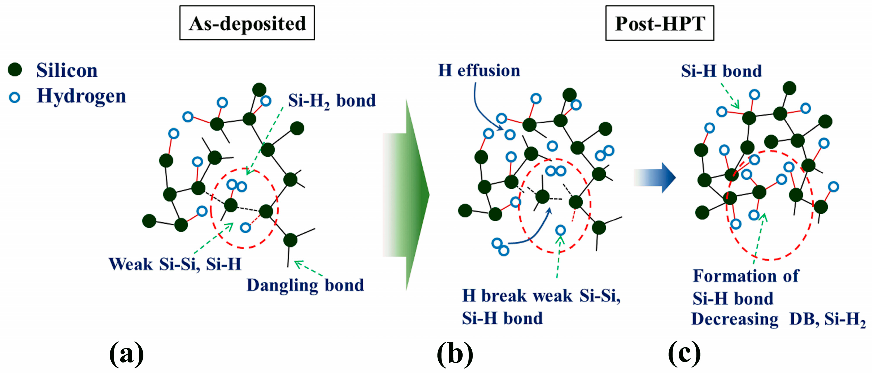
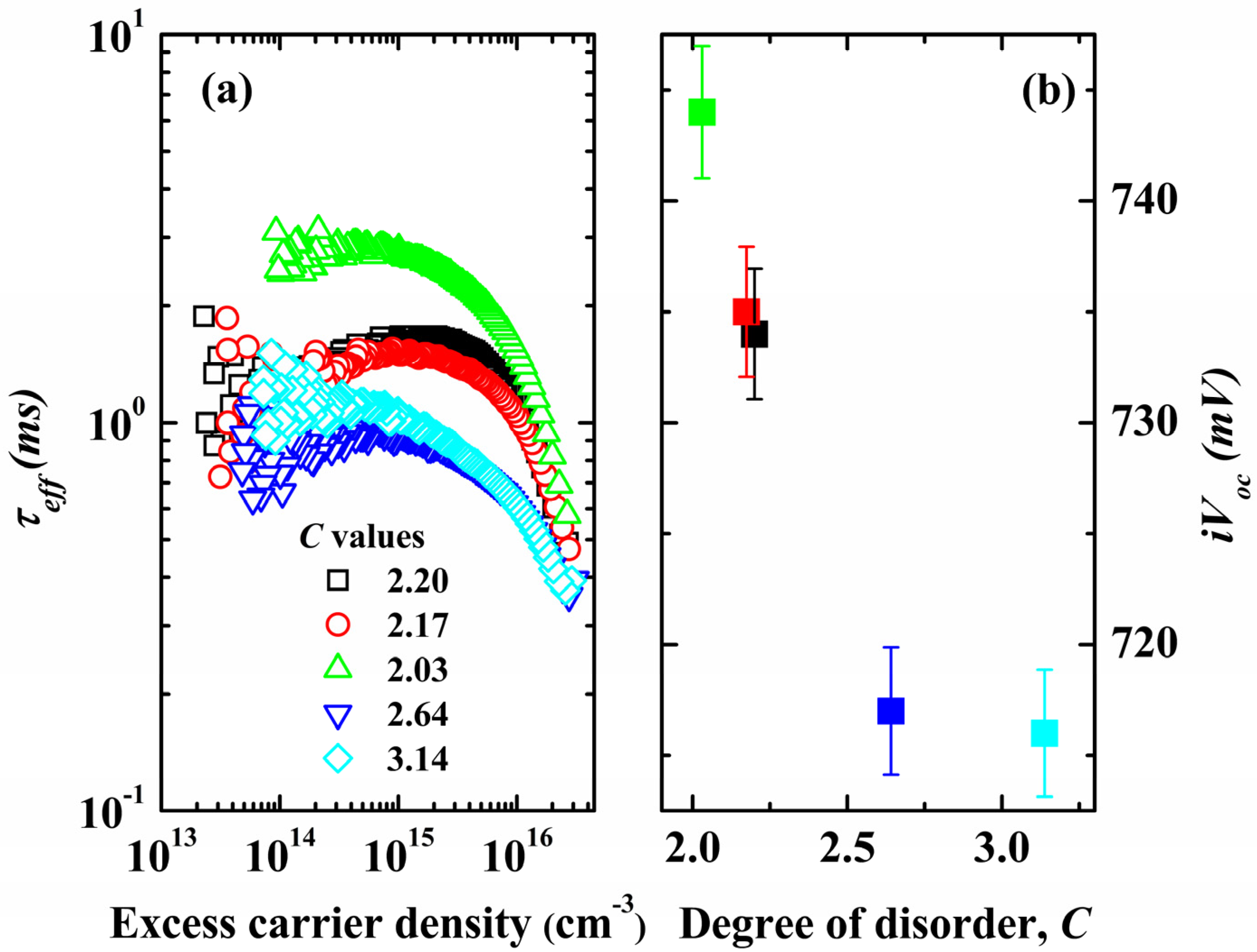
3. Results & Discussions

The microstructure of the a-Si:H(i) film was studied using spectroscopic ellipsometry. The experimental data and fitting curve for Ψ and Δ with before and after hydrogen treatments of the a-Si:H(i) layers are shown in Figure 1a. By combining the Tauc–Lorentz and BEMA fitted models [14], the maximum amplitude, <εim, max>, and the minimum amplitude, <εreal, min>, were acquired, and the results are shown in Figure 1b,c, in which the <εim, max> and <εreal, min> are related to the film density. After treatment, in the range of 0–40 W, it can be seen that the values of <εim, max> exhibited a little rise with increasing treated power, while the values of the <εreal, min> showed the opposite trend. The degree of disorder, denoted as C, is illustrated in Figure 1d. Thus, with the increase in the treatment power up to 40 W, the values of C tend to decrease. The behaviors of the <εim, max>, <εreal, min> and C inferred that after hydrogen treatment the films show fewer voids and hence, a higher structural order.
The Raman spectroscopy approach, which is effective for studying the development of ordering in amorphous silicon networks, was used to explain the ordered film network’s response to hydrogen plasma treatment power [15]. The Raman spectra of the a-Si:H layers for different treated powers as a function of the wavenumber are illustrated in Figure 2. Figure 2 denotes the Si–Si Transverse Acoustical (TA) mode, Si–Si Longitudinal Acoustic (LA) mode, and Si–Si Transverse Optical (TO) mode, which correspond to the band at around 160 cm−1, 310 cm−1, and 480 cm−1, respectively; while ΔθTO (degrees) is the bond angle dispersion, referred from [16]. Marinov et al. reported through a 216-atom model of a-Si (which was generated by the algorithm of Wooten, Winer, and Weaire) that the correlation length is associated with the vibrational mode localization state at different frequencies [17,18]. While the TO-like band is mostly sensitive to the short-range order, the high-frequency modes in the TA-like band and the LA-like band are primarily sensitive to the intermediate-range order [17]. The quantitative measures of the ITA/ITO ratios and Δθ were extracted from the peak fitting of the Raman spectra (Figure 2), as shown in Table 1. It can be seen that the ITA/ITO ratio, Δθ, and C exhibit similar trends. Initially, these values decrease as the treated power increases from 0 to 40 W, beyond which all values increase. Notably, the minimum values for ITA/ITO, Δθ, and C were obtained at the treated power of 40 W. This suggests that a more ordered network corresponds to lower C values [16,19].
Based on the information mentioned earlier, when the as-deposited a-Si:H(i) undergoes post-hydrogen treatment, the following possible situations, as depicted in Figure 3, may occur: Hydrogen atoms are effused (from hydrogen plasma) through the film surface and into its bulk. During diffusion, hydrogen atoms with preferrI confirmed kinetic energy break weak Si–Si bonds (Figure 3a,b), followed by the deactivation of not only the dangling bonds but also previously broken weak Si–Si bonds as well (Figure 3c). Thus, hydrogen atoms with higher kinetic energy, due to an increase in treated power, can exhibit greater mobility and cover longer diffusion distances. This enhanced mobility may aid in locating suitable crystal sites and subsequently adhering to them [12,16,20,21]. Therefore, it can be stated that the treated power of 40 W is the preferred power for hydrogen atoms to come into the surface, passivate dangling bonds, and break weak Si–Si bonds as well, leading to the lowest degree of disordered film. Yet, at higher-treated power levels, hydrogen treatment can adversely affect passivation. Investigating the negative effects beyond 40 W is beyond our study’s scope.
Since an a-Si:H layer plays a vital role in the a-Si:H/c-Si heterojunction solar cells, its passivated ability needs to be examined. To evaluate the correlation between the degree of disorder of the post-HPT a-Si:H(i) layer and the quality of passivation at the a-Si:H/c-Si heterointerface, we conducted an evaluation of the effective minority carrier lifetime, τeff, as a function of excess carrier density using the QSSPC method. The results are depicted in Figure 4a; in this figure, a C value of 2.20 is represented for the as-deposited a-Si:H(i) film. It is worth noting that the mean carrier density (MCD) is selected corresponding to the Vmp of the material used. However, the MCD value of 1 × 1015 cm−3 is appropriate, as it is above the noise, trapping, and dual-resonance model effects. Thus, after post-HPT, the highest τeff of 2.80 ms and the lowest τeff of 0.93 ms are achieved for the lowest C of 2.03 and the highest C of 3.14, respectively. An interesting observation is the correlation between C and τeff values, with higher τeff values corresponding to lower C values.
In addition, a recombination mechanism occurs through deep-level defects (commonly referred to as Shockley-Read-Hall [SRH] recombination). SRH recombination losses can occur at the c-Si bulk, a-Si:H/c-Si interface region, and transparent conductive electrodes (TCO). Notably, for SHJ solar cells utilizing high-quality c-Si wafers, the primary recombination loss occurs at the interface region. In this sense, excellent passivation characteristics are required to obtain a high open-circuit voltage (Voc) in an SHJ solar cell. Another interpretation of the τeff obtained through QSSPC can be used to determine the voltage of the contact device. This voltage is referred to as the implied open-circuit voltage (iVoc) and is determined by the carrier concentration at the edge of the depletion region. The iVoc values plotted as a function of the C values are depicted in Figure 4b. It can be seen that the higher iVoc values correspond to a lower degree of disorder in the films.
To understand the improvement in τeff and iVoc values associated with lower film disorder, FTIR characterization was carried out, as shown in Figure 5. The FTIR spectra, in the wave number range of 1850–2220 cm−1, were measured and represented in Figure 5a. Figure 5b displays microstructure information, MS, in the form of a bar chart. Here the MS is defined as the ratio of the integrated area under FTIR absorption spectra for a high Si-Hn stretching mode (HSM) around 2070–2100 cm−1 to that of a low Si-H stretching mode (LSM) around 1980–2010 cm−1 after de-convolution [20]. Figure 5b and Table 1 show that, as the treated power increases from 0 to 40 W, the MS ratio decreases from 11.43 to 2.88, and then increases again with further power increments. The changes in the MS ratios indicate that films treated with higher post-hydrogen treatment power have fewer voids within them. The reduced structural defect density in the films also correlates with the behavior of the degree of disorder in the layers, as discussed previously for higher-treated power (up to 40 W). It was reported that the presence voids are associated with high-order bonding, specifically Si-Hn (n ≥ 2). This bonding can have a detrimental effect on the passivation of the c-Si surface [7]. Thus, thanks to its lower structural defect density, namely the degree of disorder, these films achieved higher τeff and iVoc values, as shown in Figure 4.
Finally, the a-Si:H/c-Si HJ solar cells were constructed for evaluating the validity of our approach, and the results are illustrated in Figure 6. From the figure, it can be roughly stated that there is a negligible change in the short-circuit current density, Jsc, with alterations in the C values of the a-Si:H passivated layer. However, the behavior of other characteristics, such as Voc, FF, or η, differs from that of Jsc. The higher values of Voc, FF, and conversion efficiency can be found at the lower values of the degree of disorder, C. The behaviors of the Voc and FF are probably due to an enhancement of the τeff and subsequently, the iVoc values to a lower degree of disorder, C, as discussed earlier. The best device performance (Voc: 728 mV, Jsc: 39.55 mA/cm2, FF: 72.33%, and η: 20.84%) was achieved with the lowest C value of 2.03 and the post-HPT power of 40 W. Beyond this treated power value, nevertheless, the device characteristics dropped, and the reason for this reduction in device performance is not currently understood.
Overall, in this investigation, an interrelation was identified between the microstructure, characterized by the degree of disorder C within the layer, and the performances of the a-Si:H/c-Si heterojunction devices. Higher device characteristics, such as Voc, FF, and η, were consistently observed for lower C values, regardless of the treatment conditions. As mentioned earlier, lower C values in ordered films improve a-Si:H/c-Si heterointerface passivation, leading to higher minority carrier lifetime, and subsequent implied open-circuit voltage. This can result in improved Voc, FF, and subsequent conversion efficiency.

4. Conclusions

In this study, the correlation between the degree of disorder of the passivated a-Si:H and the performance of the a-Si:H/c-Si HJ solar cells was investigated. The results show that the post-HPT-induced rearrangement of bonds in the a-Si:H film reduced disorder within the layer, leading to an improvement in the effective carrier lifetime and the implied open-circuit voltage as well. Thus, the change in effective lifetime was attributed to microstructural characteristics, where a higher degree of disorder in the films corresponds to a lower effective minority carrier lifetime. A lower degree of disorder improved Voc and FF values, thereby increasing conversion efficiency. A maximum cell efficiency of 20.84% was obtained with the lowest degree of disorder of 2.03 in the passivated a-Si:H layer. Importantly, higher device characteristics consistently correlated with a lower degree of disorder in the films, regardless of the treatment conditions.

Author Contributions

Conceptualization, S.L. and J.P.; methodology, S.L.; software, D.P.P.; validation, S.K. and Y.K.; formal analysis, T.T.T.; investigation, S.L.; resources, J.Y.; data curation, T.T.T.; writing—original draft preparation, J.P.; writing—review and editing, V.A.D.; visualization, T.T.T.; supervision, J.Y.; project administration, V.A.D.; funding acquisition, V.A.D. All authors have read and agreed to the published version of the manuscript.

Funding

This research was funded by the Ho Chi Minh City Department of Science and Technology under grant number of 171/QĐ-SKHCN.

Conflicts of Interest

The authors declare no conflict of interest.

References

  1. Fujiwara, H.; Kondo, M. Effect of a-Si:H layer thickness on performnace of a-Si:H/c-Si heterojunction solar cells. J. Appl. Phys. 2007, 101, 054516. [Google Scholar] [CrossRef]
  2. Yoshikawa, K.; Kawasaki, H.; Yoshida, W.; Irie, T.; Konishi, K.; Nakano, K.; Uto, T.; Adachi, D.; Kanematsu, M.; Uzu, H.; et al. Silicon heterojunction solar cell with interdigitated back contacts for a photoconversion efficiency over 26%. Nat. Energy 2017, 2, 308. [Google Scholar] [CrossRef]
  3. Li, H.; Zeng, X.B.; Xie, X.B.; Yang, P.; Li, J.Y.; Zhang, Z.D.; Wang, Q.M. The amorphous/crystalline silicon interface research of HIT Solar Cells by simulation. Adv. Mate. Res. 2013, 773, 124–131. [Google Scholar] [CrossRef]
  4. Taguchi, M.; Terakawa, A.; Maruyama, E.; Tanaka, M. Obtaining a higher Voc in HIT Cells. Prog. Photovolt. 2005, 13, 481–488. [Google Scholar] [CrossRef]
  5. Wen, X.; Zeng, X.; Liao, Z.; Lei, Q.; Yin, S. An approach for improving the carriers transport properties of a-Si:H/c-Si heterojunction solar cells with efficiency of more than 27%. Sol. Energy 2013, 96, 168–176. [Google Scholar] [CrossRef]
  6. Gogolin, R.; Ferré, R.; Turcu, M.; Harder, N.P. Silicon heterojunciton solar cells: Influence of H2-dilution on crll perfromance. Sol. Energy Mater. Sol. Cells 2012, 106, 47–50. [Google Scholar] [CrossRef]
  7. Kim, S.K.; Lee, J.C.; Park, S.J.; Kim, Y.J.; Yoon, K.H. Effect of hydrogen dilution on intrinsic a-Si:H layer between emitter and Si wafer in silicon heterojunction solar cell. Sol. Energy Mater. Sol. Cells 2008, 92, 298–301. [Google Scholar] [CrossRef]
  8. Tsunomura, Y.; Yoshimine, Y.; Taguchi, M.; Baba, T.; Kinoshita, T.; Kanno, H.; Sakata, H.; Maruyama, E.; Tanaka, M. Twenty-two percent efficiency HIT solar cell. Sol. Energy Mater. Sol. Cells 2009, 93, 670–673. [Google Scholar] [CrossRef]
  9. van Sark, W.G.J.H.M.; Korte, L.; Roca, F. Physics and Technology of Amorphous-Crystalline Heterostructure Silicon Solar Cells, 1st ed.; Springer: Berlin/Heidelberg, Germany, 2008; pp. 1–12. [Google Scholar]
  10. Deligiannis, D.; Vasudevan, R.; Smets, A.H.M.; van Swaaij, R.A.C.M.M.; Zeman, M. Surface passivation of c-Si for silicon heterojunction solar cells using high-pressure hydrogen diluted plasmas. AIP Adv. 2015, 5, 97165. [Google Scholar] [CrossRef]
  11. Das, U.K.; Burrows, M.Z.; Lu, M.; Bowden, S.; Birkmire, R.W. Surface passivation and heterojunction cells on Si (100) and (111) wafers using dc and rf plasma deposited Si:H thin films. Appl. Phys. Lett. 2008, 92, 63504. [Google Scholar] [CrossRef]
  12. Descoeudres, A.; Barraud, L.; De Wolf, S.; Strahm, B.; Lachenal, D.; Guérin, C.; Holman, Z.C.; Zicarelli, F.; Demaurex, B.; Seif, J.; et al. Improved amorphous/crystalline silicon interface passivation by hydrogen plasma treatment. Appl. Phys. Lett. 2011, 99, 123506. [Google Scholar] [CrossRef]
  13. Mews, M.; Schulze, T.F.; Mingirulli, N.; Korte, L. Hydrogen plasma treatments for passivation of amorphous-crystalline silicon-heterojunctions on surfaces promoting epitaxy. Appl. Phys. Lett. 2013, 102, 122106. [Google Scholar] [CrossRef]
  14. Morral, A.F.I.; Cabarrocas, P.R.I.; Clerc, C. Structure and hydrogen content of polymorphous silicon thin films studied by spectroscopic ellipsometry and nuclear measurements. Phys. Rev. B 2004, 69, 125307. [Google Scholar] [CrossRef]
  15. Liao, N.M.; Li, W.; Liu, Z.; Jiang, Y.D.; Ma, N.; Li, Y.; Wu, Z.M.; Li, S.B. Effects of irradiation with electrons of different energies on the dark conductivity and the network of hydrogenated amorphous silicon films. Philos. Mag. Lett. 2008, 88, 871–877. [Google Scholar] [CrossRef]
  16. Park, J.J.; Iftiquar, S.M.; Lee, S.W.; Park, H.S.; Shin, C.H.; Jung, J.H.; Lee, Y.J.; Balaji, N.; Yi, J. Reduction of Tail State on P-type Hydrogenated Amorphous Silicon Oxide Films Prepared at High Hydrogen Dilution. J. Nanosci. Nanotechnol. 2013, 13, 7826–7833. [Google Scholar] [CrossRef] [PubMed]
  17. Ling, Z.P.; Ge, J.; Stang, R.; Aberle, A.G.; Mueller, T. Detailed Micro Raman Spectroscopy Analysis of Doped Silicon Thin Film Layers and Its Feasibility for Heterojunction Silicon Wafer Solar Cells. J. Mater. Sci. Chem. Eng. 2013, 1, 38124. [Google Scholar] [CrossRef]
  18. Marinov, M.; Zotov, N. Model investigation of the Raman spectra of amorphous silicon. Phys. Rev. B 1997, 55, 2938–2994. [Google Scholar] [CrossRef]
  19. Holmström, E.; Haberl, B.; Pakarinen, O.H.; Nordlund, K.; Djurabekova, F.; Arenal, R.; Williams, J.S.; Bradby, J.E.; Petersen, T.C.; Liu, A.C.Y. Dependence of short and intermediate-range order on preparation in experimental and modeled pure a-Si. J. Non-Cryst. Solids 2016, 438, 26–36. [Google Scholar] [CrossRef]
  20. Kim, S.B.; Iftiquar, S.M.; Lee, D.H.; Lee, H.J.; Kim, J.H.; Jung, J.H.; Oh, D.H.; Dao, V.A.; Yi, J.S. Improvement in Front-Contact Resistance and Interface Passivation of Heterojunction Amorphous/Crystalline Silicon Solar Cell by Hydrogen-Diluted Stacked Emitter. IEEE J. Photovolt. 2016, 6, 837–845. [Google Scholar] [CrossRef]
  21. Wolfhard, B. Basic Properties of Hydrogenated Amorphous Silicon (a-Si:H) in Thin-Film Silicon Solar Cells, 1st ed.; EPFL Press: New York, NY, USA, 2010; pp. 17–96. [Google Scholar]
Figure 1. Ellipsometry data of the a-Si:H(i) layers before and after at different treatment powers. (a) experimental data and fitting curve for Ψ and Δ; (b) maximum amplitude, <εim, max>; (c) minimum amplitude, <εreal, min>; and (d) degree of disorder, C.
Energies 16 06694 g001
Figure 2. The Raman spectra of the a-Si:H layers for different treatment powers.
Energies 16 06694 g002
Figure 3. (a) A possible bonding configuration of as-deposited a-Si:H layer; (b) hydrogen effusion following breaking week Si–Si bonds; and (c) the formation of Si-H bonds.
Energies 16 06694 g003
Figure 4. (a) Effective minority carrier lifetime vs. excess carrier density; (b) iVoc values as a function of the C values of a-Si:H thin film.
Energies 16 06694 g004
Figure 5. (a) The FTIR spectra; and (b) the information of the microstructure, MS, of the a-Si:H(i) passivated layer at different treatment powers.
Energies 16 06694 g005
Figure 6. The correlation between the efficiency and other parameters of the a-Si:H/c-Si HJ solar cells and the degree of disorder of passivated a-Si:H thin films as a function of treatment powers.
Energies 16 06694 g006
Table 1. The summaries of some micro-structural properties of the a-Si:H layer, such as the degree of disorder, CITA/ITO, ΔθTO, and MS (%).
Treated Power (W)CITA/ITOΔθTOMS (%)
02.200.407.8211.43
302.170.397.213.09
402.030.376.822.88
502.640.397.034.55
603.140.418.1517.38
Disclaimer/Publisher’s Note: The statements, opinions and data contained in all publications are solely those of the individual author(s) and contributor(s) and not of MDPI and/or the editor(s). MDPI and/or the editor(s) disclaim responsibility for any injury to people or property resulting from any ideas, methods, instructions or products referred to in the content.

