1. Introduction
The recent growth of areas of green energy harvesting (e.g., solar, wind) [
1] and utilization (e.g., electric vehicles) [
2] is driving the development of power conversion systems and electronic components with the aim of optimizing efficiency and power-energy density [
3]. At the same time, the development and growth of wide-band-gap (WBG) semiconductors makes it possible to achieve increased efficiency when operating at higher voltages and frequencies, with fewer temperature limitations [
4].
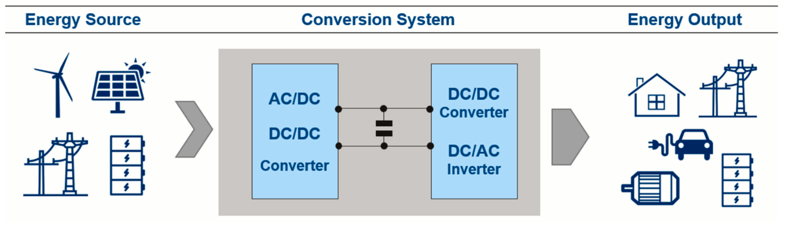
In most power converters, the input stage converts voltage from AC or DC to a desired intermediate DC level; then, the output stage converts this DC to either AC (induction motors, powertrain, AC power lines) or different voltage DC (battery charge). The intermediate DC voltage section (DC link) includes a specific DC-link capacitor with the function of a buffer, providing and absorbing the high-frequency current surges from and to the converters and low-frequency current spikes during transient periods. This allows input and output converters to operate correctly at the same time, with different frequency and duty cycles.
Figure 1 indicates the placement of the DC-link capacitor in a general conversion system [
5].
DC-link capacitors operate under constant high-voltage DC bias, with a heavy ripple current superimposed when power conversion is active, so the main characteristics for proper operation at high efficiency can be summarized as follows:
High electric field: the energy density of a capacitor corresponds to electric field squared, so the effect of reducing the dielectric thickness for a given voltage is very significant.
Low equivalent series resistance (ESR): this results in low heat generation with ripple current or makes it possible to apply high ripple current for the dissipation of heat from the system.
Safety and reliability: with high-power and high-energy devices, failure to short circuit must be avoided in order to prevent catastrophic failures of the entire system.
Metallized film capacitors are often the best choice for such applications [
6], as they have higher reliability and performance compared to alternative capacitor technologies [
7,
8]. Polypropylene film, in particular, is the most frequently used, because of its ability to withstand high voltage (up to 700 V/µm), its intrinsically low ESR (dissipation factor lower than 0.02%), and its graceful failure mode (self-healing), which allows operation at high energy and high power density without compromising on size. The best volumetric efficiency can be obtained for operational voltages in the range of 300–2000 V, such that existing BOPPs (thickness 2–10 µm) can operate at optimum electric field (above 150 V/µm). In addition, polypropylene is a cost-effective dielectric, allowing it to be employed in many applications.
By analogy with the trends set by the evolution of power converters and the introduction of wide-band-gap (WBG) semiconductors, the development of polypropylene DC-link capacitors is directed toward two main targets: miniaturization and increased operating temperature [
9].
Miniaturization of capacitors: this allows reduction in volume and weight, together with the potential improvement of equivalent series inductance (ESL) deriving from reduced lengths. In automotive powertrain applications, film thickness in the range 2.4–5.0 μm is used for the two main platforms 450 V and 850 V, with electric field in the range of 150–200 V/μm. Next-generation DC-link capacitors are required to operate above 250 V/μm in order to meet miniaturization requirements.
Increase maximum operating temperature to 115 °C: DC-link capacitors now operate at up to 85–105 °C, depending on size and application [
10]. In automotive powertrains, the extension of the temperature range allows higher power transfer and a reduction in auxiliary cooling systems.
With BOPP films, the dielectric constant and dissipation factor will only change slightly with temperature and electric field, so the expected effect on capacitance and ESR will be minimal under the new target conditions. On the other hand, the combination of increased thermal and electrical stresses has a synergistic effect on some other electrical properties, in particular on electrical conductivity or insulation resistance of the dielectric. Polypropylene film capacitors are often used in applications in which negligible discharge rates are required, because of their high insulation resistance (IR) and low conduction current, or leakage current (LC). In any case, IR can be decreased by more than three orders of magnitude if temperature and electric field are increased simultaneously to their maximum levels.
The conductivity of the dielectric material and its dependency on temperature and electric field become key factors in the development of next-generation BOPP films for use in extreme conditions. Considering recent trends, it is possible to expect further increases in temperature requirements in future applications, with polypropylene remaining the dielectric of choice at temperatures up to 125 °C.
The aim of this work is to review the key mechanisms involved in the electrical conduction of ultra-thin polymeric films, with a focus on isotactic polypropylene films, at the voltages and temperatures typical of automotive DC-link capacitors. The aim is to provide a comprehensive description of the phenomena involved in the process, an understanding of the deviations from the ideal, and provide methods for evaluating the conductivity of real capacitors.
2. Conduction Current in Polypropylene Films
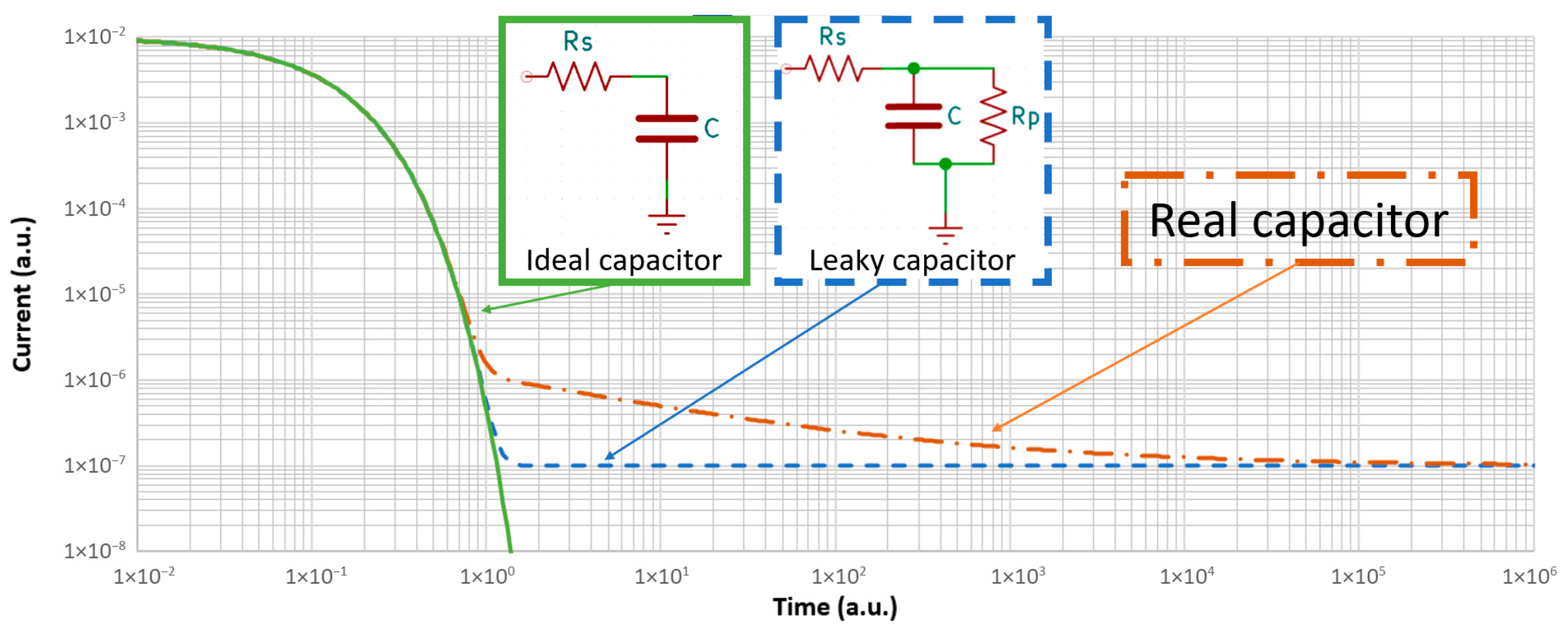
When DC voltage is applied to a capacitor or dielectric film sample, the current will evolve with time through several phases.
Figure 2 presents the current trend with time for a 1 µF capacitor energized via a 100 kΩ series resistor at three different levels of approximation: the ideal capacitor, the typically used lumped element model for a leaky capacitor, and the simplified curve for a real film capacitor.
The ideal capacitor of
Figure 2 is charged through the series resistance Rs, with current following an exponential decay according to (1):
where
i1 is the current,
V is the applied voltage,
t is time, and
τ is the time constant of the RC circuit (product of capacitance C and series resistance R
s). The time constant helps estimate the duration of charging, with 99.9% of charging complete after 6τ (0.6 s in this example). During the charge phase, charge carriers accumulate on the electrodes, and the dielectric polarizes. No current flows through the dielectric, and in the external circuit, the current will asymptotically converge to zero.
The non-ideal capacitor with simplified equivalent circuit shown in
Figure 2 will initially charge in a manner similar to that of the ideal capacitor (if
Rp is considerably larger than R
s, as in the example case). The intrinsic ESR of the non-ideal capacitor is neglected, because it is expected to be considerably lower than other resistors in the circuit (typically 10
−4–10
0 Ω in film capacitors). Instead of converging to zero, the current would stabilize at a certain level, corresponding to the leakage current, according to:
where
i2 is the steady-state current,
Rp is the parallel (leakage) resistor, and other variables are as previously defined. With this model,
i2 is unchanged after the charge phase is complete, because V, Rs and Rp are independent of time, and the exponential term becomes negligible after a period of a few time constants. For the given example, the external series resistor Rs can be ignored, resulting in:
Equations (2) and (3) are the generally accepted equivalent circuit representing capacitors with a leakage component, and are particularly valid when the parallel resistance term is low, giving rise to high leakage current.
Real plastic film capacitors (and many other dielectric types) exhibit a three-phase characteristic curve, as shown in
Figure 2, with polarization, absorption, and steady-state current. The initial and final phases are equivalent to the non-ideal capacitor model.
The intermediate phase is a slow current decay transient in which current is almost always found to follow a power dependency with time. This trend, found in many dielectrics, is known as Curie–Von Schweidler (CvS) law [
11,
12]:
where
n is an exponent, usually found to be between 0.2 and 1 with BOPP and other common dielectrics. The duration of this phase can range from 10
3 to 10
6 s, with a few authors suggesting that it may extend indefinitely in time [
13]. The CvS phase is not predicted by the lumped-element model of
Figure 2, and the mechanism of this phase has not been fully clarified and agreed upon [
14,
15]. For this reason, Equation (4) is given in the form of a general proportionality. The more plausible explanation of the CvS law decay is related to charge injection and the progressive modification of the local electric field within the dielectric and at the electrode–dielectric interface [
16,
17], but several other theories have been proposed [
13,
14,
18,
19,
20]. The CvS transient phase is often neglected in characterization works, where it is considered a stabilization phase, and very few data are available for review. Anyway, the importance of this phase in real-world applications must be highlighted: with durations exceeding hours and days, it may represent a significant fraction of the operating time in application. Moreover, because industrial testing procedures for practical reasons need to limit the stabilization time to few minutes or seconds, the measured LC and conductivity values may overestimate considerably the ultimate steady state value measurable at long time.
If sufficiently long stabilization periods are used, assuming that stabilization will take place after a certain CvS decay time, the non-ideal capacitor approximation might still be considered for simplicity, and experimental results could be fitted according to (2) and (3) for the determination of Rp. Insulation resistance or conductivity in real dielectrics is a function of temperature and electric field, so Equation (3) will be substituted by more complex equations, depending on the conduction mechanism of choice. This will be discussed in more detail in the following paragraphs, after the necessary overview of the principles that determine the interaction of electrons with polymeric dielectrics.
3. Chemical Structure
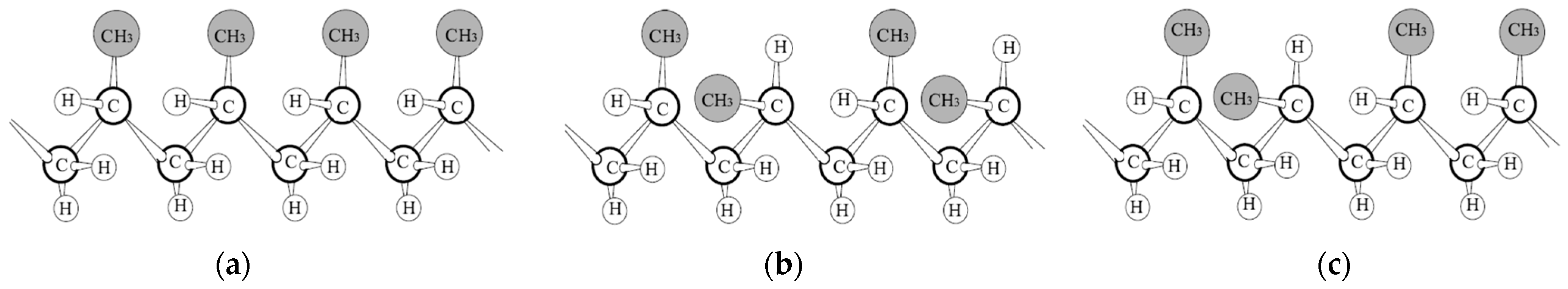
Polypropylene belongs to the family of polyolefins, which are macromolecules obtained through the polymerization of olefins. The backbone of the polymer consists of saturated carbon repeating units, as depicted in
Figure 3, with one methyl (-CH
3) side chain at each repeating unit. The carbon and hydrogen composing its structure have very similar electronegativity, resulting in only slight bond polarization and an overall null dipole moment. This makes polypropylene a nonpolar polymer, which is key to its low dissipation characteristics. For the same reason, the interaction forces between different polymer chains are mostly limited to weak Van der Waals dispersive forces. Cohesion between different molecules and good mechanical properties require high molecular weight and ordered polymeric chains to maximize interactions. The methyl side chains play a critical role in these aspects, making polypropylene substantially different from polyethylene. Polypropylene is in fact a stereo-specific polymer: the tertiary carbons in the polymer chain are chiral centers, and the whole polymer is characterized by a certain “tacticity”, the long-range regularity of chiral centers. Tacticity can have a substantial effect on the properties of a polymer, in fact the first obtained polypropylene, with no stereo-regularity, was not particularly appealing for industry. The lack of regularity in the sequence of chiral centers resulted in very weak intra-chain interactions and an amorphous structure, limiting the strength of the material and its possible applications. It was with the revolutionary introduction of stereospecific catalyst [
21], enabling the synthesis of non-branched, long, stereo-regular polymers, that polypropylene became the ubiquitous material that is today.
Figure 3 shows the three possible configurations of polypropylene. Isotactic (all chiral groups with the same orientation) and syndiotactic (alternating chiral orientation) polypropylene can both interact with one another at closer range, resulting in higher attraction forces and greater probability of forming extended crystalline structures than atactic polypropylene (no stereo-regularity). Isotactic polypropylene is the most frequently used type for electrical applications, and most of the reviewed papers refer to this isomer. Syndiotactic polypropylene has also been reported for use in electrical insulation applications, with some authors suggesting potential advantages over the isotactic isomer, thanks to the multiple stable morphologic structures of this isomer [
23,
24]. Anyway, only isotactic polypropylene is currently available in thin films for capacitor applications.
Tacticity in general will not extend indefinitely over the whole polymer chain, so additional attributes must be introduced to define polypropylene grades, like the tacticity degree (the amount of polymer chain characterized by ordered structure) or meso-sequence length (the number of adjacent repeating units with the same stereoregularity). Capacitor-grade polypropylene is generally over 95% isotactic, with recent high-performance resins exceeding 98%, thus making them able to form very highly ordered structures, and reach the highest crystallinity. Contrary to inorganic materials, polymers never exhibit complete crystallization, and ordered crystalline regions are interleaved with disordered structures called amorphous regions, in which chain interaction is lower and mobility is higher. In the case of films obtained by stretching methods, in particular, biaxially oriented films, drawing gives additional regularity to both crystalline and amorphous regions, resulting in the generation of stretching-induced order [
25] with increasing crystallinity. The electrical and mechanical properties of oriented films are generally superior compared to the precursor unstretched material.
4. Electronic Structure
Electrical conduction through a material requires the movement of charges upon application of an electric field (drift). With polymers, “electronic” conduction is generally assumed, based on the drift of the electrons or holes, unless contaminants are present to give rise to ionic conduction. Electrons can only be found at determined energy levels on existing orbitals, and drift must take place from and to such levels. Deviations of real polymeric films from ideality were anticipated in the previous paragraphs, and will be further investigated here, at an electronic level, to help understand the possible paths (in space and energy) that electrons can take when under the influence of an imposed electric field.
Polymers in general can be considered to be wide-band-gap insulators, with band-gap energy estimated to be in the range of 5 to 8 eV [
26,
27] in the case of isotactic polypropylene. The electronic structure of organic molecules, the molecular orbitals, can be theoretically derived from atomic orbitals by linear combination of their wavefunction (LCAO). With a large number of orbitals, it is convenient to describe their distribution along the energy coordinate by the Density of States (DOS): the number of energy states present at each energy level. As the number of atoms and orbitals increases, they may form almost continuous spreads of electronic states at some energy levels, similar to electronic bands of crystalline materials. According to the Aufbau principle, electrons populate states and bands from the lowest energy. Filled orbitals are identified as a valence band and non-filled orbitals correspond to a conduction band [
28]. Transitions from occupied to unoccupied orbitals/bands are then possible when the correct amount of energy is provided, usually in the form of thermal energy or electromagnetic radiation. Above absolute zero, a dynamic equilibrium between energy levels must always be expected, according to the Fermi–Dirac distribution (5).
where
P is the probability of having an electron at the energy level
E,
EF is the Fermi level,
kB is Boltzmann’s constant, and
T is the temperature.
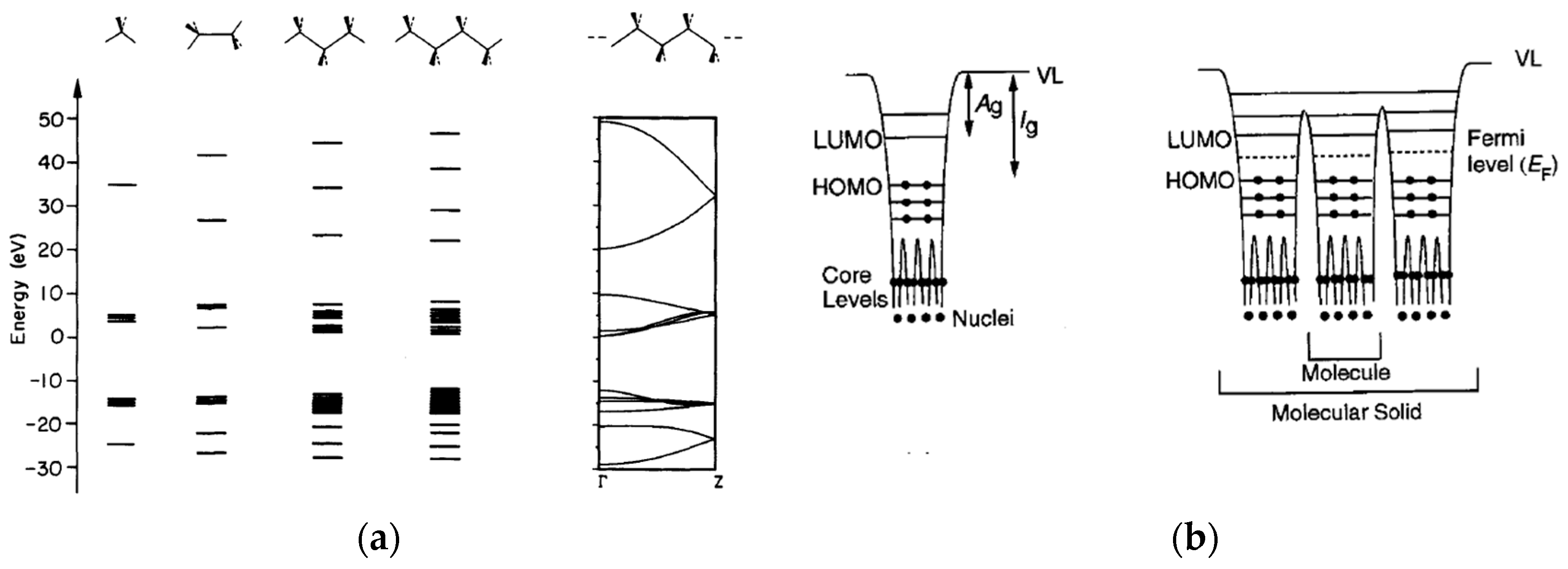
Hoffmann described the construction of electronic bands of polyethylene from single atoms to short-chain alkanes, giving a valuable description of both the chemical and the electronic approaches on the subject [
29].
Figure 4a shows how molecular orbitals evolve as the number of carbons increases, forming continuous bands with polymer-sized molecules.
Ishii gives further insight into the band structure of organic molecules, with particular focus on the effect of contact between different materials, as with conductor/insulator interfaces [
30] that are necessarily formed when assembling a metal–insulator–metal (MIM) capacitor structure. In addition to the obvious metal–insulator interfaces, additional electronic discontinuities are present at molecule-to-molecule and phase-to-phase transition points.
Figure 4b extends the visualization of molecular orbitals from single molecule to arrays of molecules, including the energy wells that develop in space between orbitals. With this representation it is possible to see that the band structure must interrupt at molecule-to-molecule transitions, with a locally very low density of states at such interfaces. In other words, the conduction band will be at a higher energy level in the intramolecular space, with significant energy barriers for the leap of electrons from one molecule to the other.
When a heterojunction is formed, namely, every time different materials are put in contact, including metal and different polymer chains or different phases, the Fermi levels of the two materials must converge to maintain constant chemical potential of electrons across the materials [
31]. The equilibrium is established through charge transfer between the materials, and in the case of polypropylene in contact with metals, electrons are generally transferred from the metal to the polymer, with a relative shift of the band levels [
32] and bending of band edges of the polymer [
33]. With respect to electrodes, the high reactivity of metals in the conditions of deposition onto organic substrates likely results in chemical reactions between the two or diffusion of metal into the organic layer, thus generating an additional interlayer with a distinct electronic structure.
The LCAO method can be further extended, resulting in what is referred to as the “first-principle” method, allowing the derivation of energy states of large molecular solids. The introduction of structural non-uniformity, interfaces and chemical or physical variations (defects) makes the calculation of molecular orbitals (electronic bands) of polymers an extremely complex problem to solve, even for simple polyolefins. First-principle calculations today are mostly accomplished through the application of Density Functional Theory (DFT), a computational method based on electron density, which is a simpler solution compared to wavefunction calculations.
The simulation of complex arrangements of polymer chains, including deviations from pure crystalline structure and chemical modifications, is a valuable approach for the study of electronic properties of materials. Any change in chemical or spatial structure will give rise to different orbitals interactions and change in the resulting electronic band structure. Consequently, the electron population along the energy coordinate (DOS), too, will be modified. In particular, when new states form at previously unpopulated energy levels (i.e., within band gaps, where density of states was zero for the perfect polymer crystal), the effect on the electronic properties of the material will be significant. These “new states” are referred to as localized states and may reduce the band gap or provide intermediate steps within the band gap, facilitating the promotion of electrons or offering intermediate stable states for electrons within the bandgap. For this second reason, they are often called “traps”. The different types of defect and deviations from the ideal will be analyzed in depth in the next section.
5. Physical and Chemical Defects
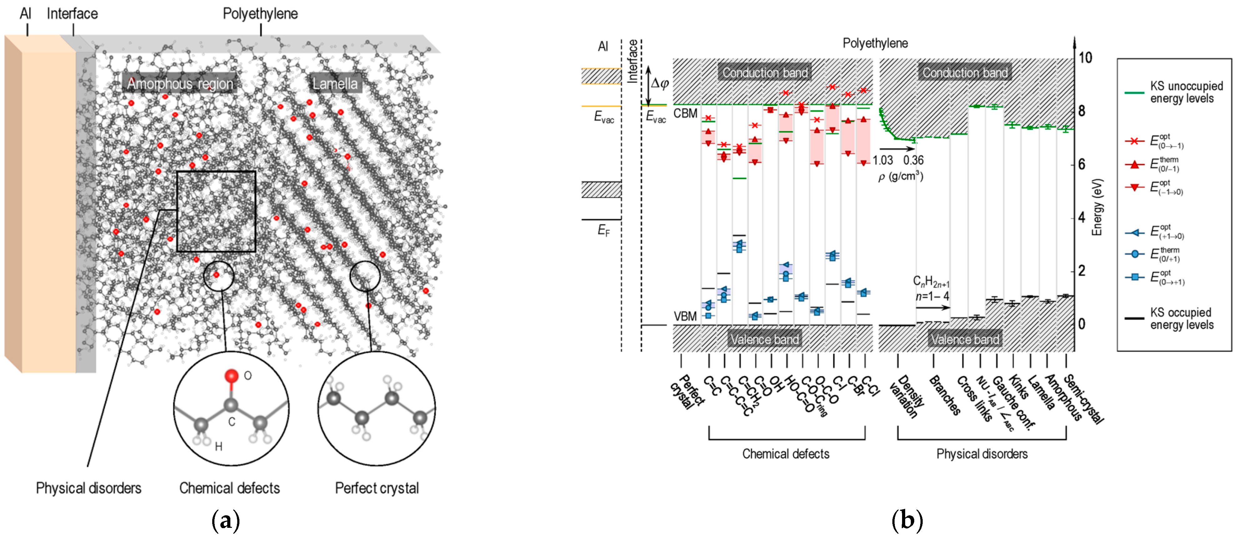
Physical and chemical variations in a perfect polyolefin crystal structure will modify its band structure, with local shifts in the energy level of bands and the appearance of new accessible energy levels [
26,
34]. The spatial localizations of defects and the calculated effect of their presence on the band structure are depicted in
Figure 5.
Intuitively, the pure crystal form is characterized by a larger and sharper band gap, extending homogeneously through the whole volume of the material.
The local introduction of new atoms and the change in their oxidation state (including the hybridization of carbon atoms) on the polymer chain can modify the electronic structure considerably, with rearrangement of existing states and formation of new states, which may fall at previously unpopulated energy levels. Moreover, the presence of polar groups and dipoles in a generally nonpolar matrix such as polypropylene will have an additional effect on the local electric field perceived by the surrounding unmodified polymer chains, distorting the electronic structure at longer ranges [
35]. A similar effect must be expected when polar contaminants or additives are introduced into the matrix, even if not directly bonded to the polymer chains. All these modifications are referred to as “chemical defects”, and the most important effect on the electronic structure is the formation of localized states (localized both in space and energy) or “traps”. Localized states are isolated from the conduction and valence band, as indicated with red and blue dots in
Figure 5b.
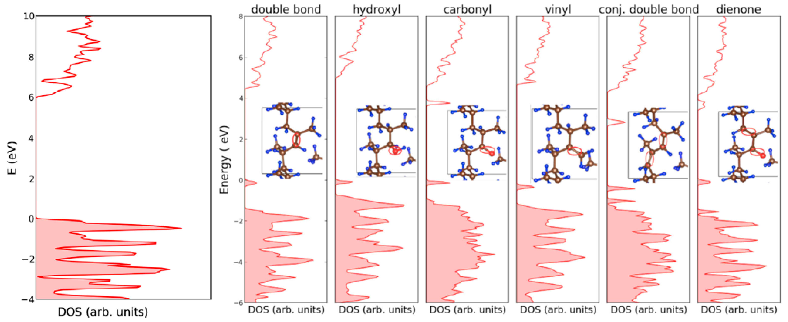
The DOS distribution of polypropylene is illustrated in
Figure 6, with the introduction of common chemical defects. It is possible to see that the entire distribution of states is affected by chemical modification, as well as the newly formed states within the bandgap. In the case of chemical defects, the energy separation of the newly localized states from the conduction band minimum (CBm) and from the valence band maximum (VBM) can be high; therefore, they are referred to as “deep traps”.
Changes in the spatial distribution of polymeric chains, such as a transition from a crystalline to an amorphous structure, or minor chemical variations like with branching and changes in tacticity, will also modify the interactions between polymer chains and their orbitals. These are referred to as “physical defects”, and have a less pronounced effect on the electronic structure compared to chemical defects, resulting in the broadening of the DOS distribution and a diffuse reduction in the bandgap or occasional formation of localized states in proximity to the VBM or CBm. By analogy with the deep traps formed by chemical defects, these states are referred to as “shallow traps”. In the case of physical defects, not only are the energy deviations from the pure crystal small and diffuse, the transition in space is also expected to be smoother compared to in deep traps because of the close-range interaction of potential wells, which tends to reduce the height of the energy barrier between adjacent traps [
37].
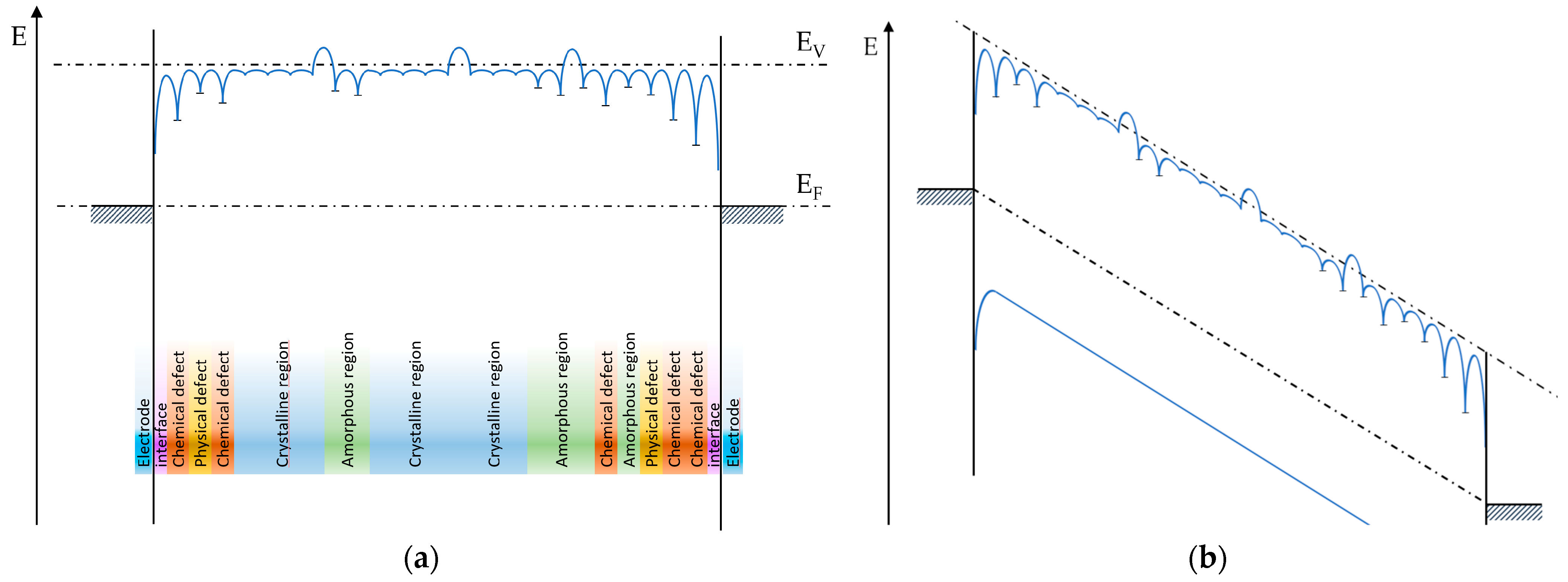
Considering a non-ideal material, physical and chemical defects will be distributed within its volume, affecting only a minor fraction of the matrix. Certain defects can be randomly distributed (crystal-phase transitions and well-dispersed additives), while others could show a certain density gradient (the crystal phase interruption at the electrodes or chemical defects caused by diffusion-controlled reactions with external agents, such as oxidation).
Figure 7a exemplifies a possible distribution of defects and consequent pathway for electrons through the different accessible levels. Charge carriers will have to cross multiple electronic structures along their path in space, with a consequent change in accessible energy levels, and potential discontinuity of the bands at transitions between polymer chains. The effect of voltage application between the electrodes is presented in
Figure 7b, showing that traps represent local minima in a highly spontaneous overall pathway. It must be underlined that
Figure 7b is represented not to scale for clarity, as the energy separation of electrodes under the conditions of interest and the bandgap or trap depths are on different energy scales (hundreds of eV and units or fractions of eV, respectively).
Conduction from electrode to electrode is a thermodynamically favorable process because of the difference in energy between the two electrodes, but it is limited by the mobility and availability of charge carriers. Several theories and models exist to predict the value of current through the dielectric, given the electronic structure of the system, and will be discussed in the next section.
6. Conduction Mechanisms
Steady-state conduction in insulating materials has been studied since the beginning of the last century, and most conduction theories were formalized before 1950, first for vacuum phenomena, and later for crystalline inorganic materials. In the following years, these were also extended to organic dielectrics, including crystalline and amorphous polymers with the addition of minor corrective terms.
Because of the electric field applied to the sample, electrodes are at different energy potentials, and the drift of both electrons and holes represents a thermodynamically spontaneous phenomenon, limited by the availability of free charge carriers and the kinetics imposed by energy barriers along the path. When, within the dielectric, electrons are only able to transit on existing energy levels or bands, as shown in
Figure 7, several energy steps must be passed, and several mechanisms might be active at the same time in different locations on the dielectric [
38]. The emission of electrons from orbitals to the vacuum level (ionization of the molecule) is also a potential pathway for conduction, in particular for wide-band-gap dielectrics like polyolefins, in which localized states and the minimum conduction band level lie close to the vacuum level, potentially with higher energy.
All steps contribute to the drift rate, but if one phase is significantly slower than the others, which in general can be expected, this phase will become the limiting step, defining the overall drift rate through the dielectric. Several authors have suggested that molecule-to-molecule transitions and, more generally, transfers at the interface between different materials or phases within the material represent the limiting steps in conduction [
39,
40]. Further consideration of
Figure 7 suggests that the existence of conduction processes with different rates implies that sections of the dielectric will experience an increase or decrease in charge density (formation of space charge), with consequent distortion of the internal electric field and lengthening of polarization phenomena.
In the first approximation, charge drift can be distinguished into three main types, based on the position at which the process takes place: injection, transport, and extraction mechanisms, depending on whether the charge transfer is from electrode to dielectric, from dielectric to dielectric, or from dielectric to electrode, respectively. Analogously, based on where the limiting step is located, the overall conduction can be defined as being injection, transport or extraction limited. In BOPP conduction studies, the extraction step is generally neglected, assuming a lower energy barrier [
41]. Moreover, because of the electron/hole duality, extraction can be assimilated to an injection of the opposite charge carrier, and despite energy barriers presumably being different, the equations and trends should not change from injection to extraction. For this reason, only injection-limited and transport-limited mechanisms will be presented.
The most relevant injection and transport mechanisms for the study of dielectrics are analyzed in reference to MIM structures. These are to be considered as the basic building blocks for the study of conduction in insulators, and the literature reports several proposed modifications, improvements and combinations of models to better fit the experimental data [
42,
43].
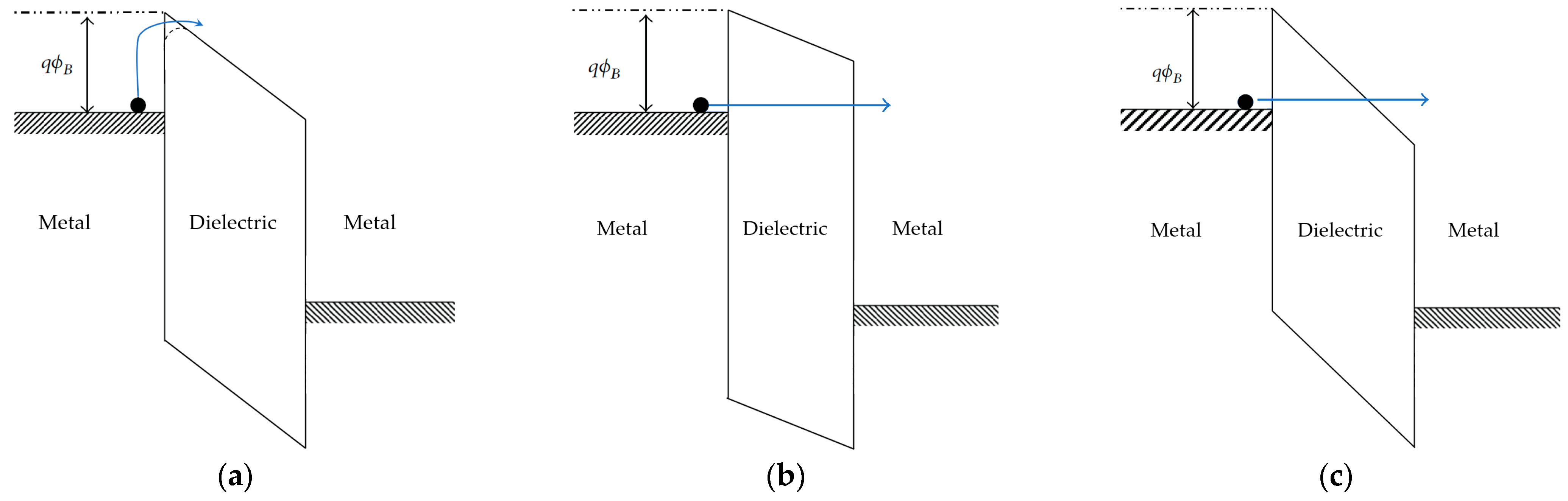
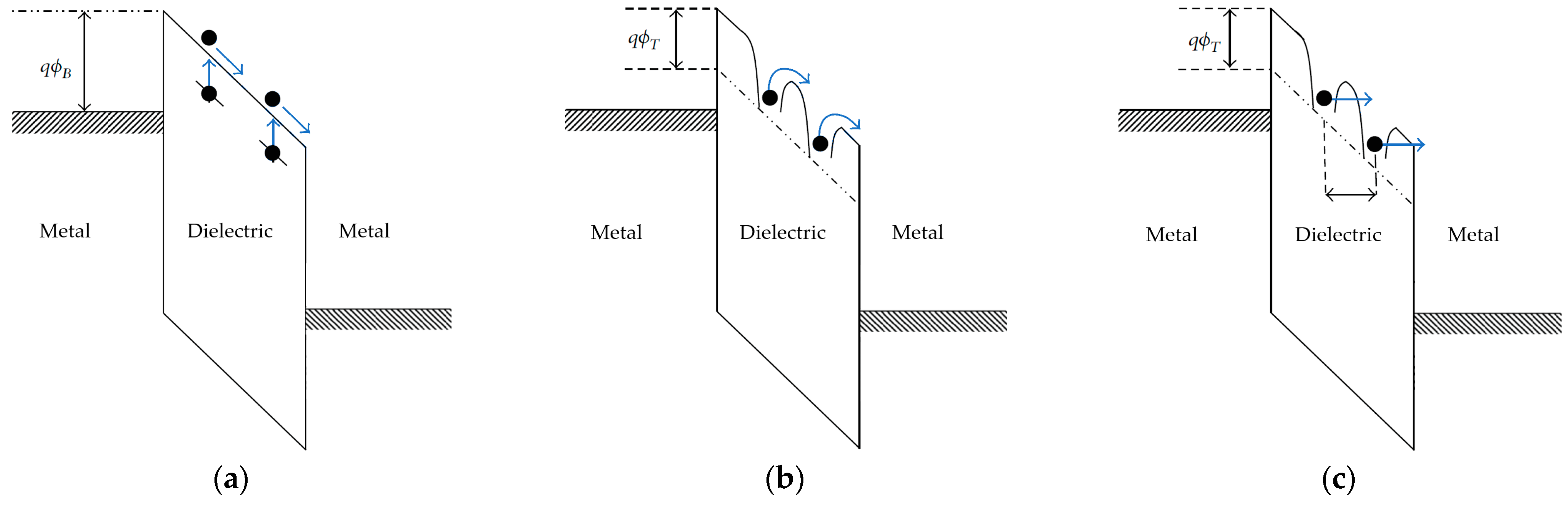
6.1. Injection-Limited Mechanisms
For injection to happen, charge carriers need to overcome the energy barrier formed between the Fermi level of the electrode and the conduction band or localized states of the insulator at short distances from the electrode surface. The most intuitive way to overcome the barrier is with electrons possessing sufficient energy in the form of thermal energy, resulting in the thermionic emission of electrons to the dielectric. In the case of metal–polymer interfaces, the predicted barrier height is generally very high, because of the high band gap of the polymer. With BOPP and common metals, the energy barrier is on the order of 4 eV, which, according to Equation (5), corresponds to a probability of 10−54; thus, a negligible number of carriers possess sufficient energy to pass the barrier at common temperatures.
Because experimentally measured conductivity is several orders of magnitude higher than that calculated from “pure” thermionic emission with 4 eV barrier, alternative lower-energy mechanisms must be considered to explain such deviations.
Figure 8 indicates three frequently considered injection mechanisms that can be used to better fit the experimental results.
6.1.1. Schottky Emission
When an electric field is applied across the insulator, the band structure of the dielectric will tilt, with a slope proportional to the electric field. In addition to this, the Schottky effect predicts that the energy barrier at the interface will also be distorted, taking on a rounded shape, as shown in
Figure 8a. The energy barrier for charge injection to the conduction band of the dielectric will be lowered, so a larger number of charge carriers will have sufficient energy to enter the conduction band from the Fermi level of the electrode. The higher the electric field, the higher the distortion and corresponding reduction of the energy barrier. Schottky’s emission mechanisms predict the current density of charge carriers injected from the electrode to the conduction band of the dielectric, as follows:
where
J is current density,
A is the Richardson coefficient,
T is the temperature,
q is the charge of the electron,
ΦB is the original energy barrier,
E is the electric field on the insulator,
εrε0 is the dielectric constant of the insulator,
kB is Boltzmann’s constant, and
h is Planck’s constant. The depth in the dielectric at which the barrier maximum is found depends on the characteristics of the dielectric (Φ, ε
r) and applied conditions (E). With polypropylene at 250 V/µm, it is just below 1 nm.
It must be emphasized that the energy barrier reduction according to Equation (6) for polypropylene under the conditions of interest will be less than 0.5 eV. Such a decrease in the energy barrier will not be sufficient to fit the experimental data; when Φ is close to the theoretical value of about 4 eV, the calculated current will still be extremely low. The fitting of the experimental current measurements can be achieved with Φ values of around 1 eV, and this could be justified in consideration of surface traps or accessible states at lower energy.
6.1.2. Direct Tunneling (DT)
According to quantum mechanics, electrons are described by a wavefunction, with their position being defined in terms of probability distribution, which fades to zero only at infinity. This means that electrons at the metal–insulator interface have a non-zero probability of passing through the barrier, or across the barrier, despite not having sufficient energy to pass it. This mechanism is called direct tunneling, and it is considered to occur when the dielectric is so thin that the wavefunction demonstrates a significant probability of passing across the dielectric thickness. The limit thickness is in the range of a few nanometers. A high electric field can promote tunneling by distorting the wavefunction of the electrons. Temperature has no effect, because thermal activation is not part of the injection mechanism, as can be seen from the diagram in
Figure 8b and from the characteristic equation, as determined by Tsu-Esaki [
45]:
where
m is the electron mass,
TC is the transmission coefficient, which in turn is the function of the electric field and the electron mass in the dielectric, and
N(Ex) is the supply function, and other quantities were previously defined. Direct tunneling may occur when the temperature is low, so that other thermally activated injection mechanisms are inactive. Direct tunneling has the peculiarity of transmitting charge directly from electrode to electrode, so that no additional transport mechanism is necessary for conduction. Some authors have suggested that tunneling may take place within polymer dielectrics at the molecule-to-molecule energy barriers, where other mechanisms may not be active [
39]. Such transitions are characterized by high energy barrier values because of the separation between molecular orbitals, and the distance is expected to be in the range of a few angstrom units.
6.1.3. Fowler–Nordheim (FN) Tunneling
With dielectric thicknesses larger than about 10 nm, direct tunneling becomes extremely improbable. In the presence of high electric field, the energy barrier is distorted (inclined) such that charge carriers may pass through the triangular part of the barrier, in a manner equivalent to tunneling through a thinner barrier.
Figure 8c depicts this pathway. This mechanism is called Fowler–Nordheim tunneling (FN). The magnitude of current density is given by:
where
is the tunneling effective mass and other quantities are as previously defined.
By analogy with direct tunneling, FN tunneling is independent of temperature, and thus can be considered to occur at low temperature and high field, when other thermally activated injection mechanisms are inactive. FN tunneling predicts charge injection from the electrode to the conduction band in the bulk of the dielectric, instead of from electrode to electrode, as in the case of DT. Additional conduction through the dielectric must be considered to complete the charge transfer.
6.2. Transport-Limited Mechanisms
In the presence of traps, after injection, the conduction proceeds via continuous trapping and de-trapping steps until the extraction electrode is reached. With reference to
Figure 7b, the trapping phase is spontaneous to intermediately stable states, while energy is required to overcome the de-trapping steps. The simplest thermal-excitation-based de-trapping process is not always able to describe the dependency of conductivity with temperature and electric field, so additional mechanisms are often introduced to fit experimental observations. The most common transport mechanisms are depicted in
Figure 9 and described in the following paragraphs.
The previous analysis of polymeric dielectrics suggests a multi-trap-level model, but for the sake of simplicity, and by derivation from more homogeneous crystalline dielectrics, the band gap is often considered to be of constant width with a single trap depth corresponding to a single de-trapping energy barrier. Despite not being formally correct, this approach will be justified considering that the overall current will be defined by the single most limiting active conduction process. More complex models with variable trap depth distribution are sometimes considered. These usually include an exponential trap distribution to represent the real density of states near the conduction band or account for the expectedly higher surface defectivity [
46,
47]. Because of the added complexity, such models are mostly found in computational works, often aimed at determining the space charge within the dielectric.
6.2.1. Ohmic Conduction
Ohmic conduction refers to a mechanism in which the conductivity is not dependent on the electric field, so the current is linearly proportional to the applied voltage, according to Ohm’s law. With proper ohmic conductors, conductivity is inversely proportional to temperature, because thermal vibrations tend to increase the number of impacts and reduce the mean free path of charge carriers and their mobility. With insulating materials and plastic dielectrics, the opposite behavior is frequently observed, with an exponential increase in conductivity with temperature, analogously with the Arrhenius reaction rate for thermally activated processes. This can be accounted for considering the process as consecutive steps of conduction and trapping as indicated in
Figure 9a. The limiting step is the excitation of charge carriers to reach the conduction band. Considering the Fermi–Dirac distribution, the number of excited charge carriers increases with increasing temperature, so that more of them have sufficient energy to overcome a given potential barrier, according to:
where
n and
µ are the number and mobility of charge carriers, respectively,
N is the density of states in the conduction band, and Φ is the energy step to overcome. At any given temperature, current and conductivity will be linearly dependent on the electric field. With a defect-free crystalline polypropylene (Φ = E
F − E
C ≃ 4 eV), the calculated current would be negligible at any reasonable temperature, as anticipated in the case of Schottky injection. The fit of experimental data is possible considering the intermediate energy levels provided by deep and shallow traps (Φ = E
T − E
C ≃0–1 eV, with E
T being the energy level of traps).
This simple scenario is quite realistic at low voltage, where the effects of electric field on the electronic structure and distortion of energy barriers are minimal, as will be discussed in the experimental data analysis section. In fact, several of the proposed transport mechanisms tend towards a linear, ohmic approximation as their low electric field limit.
6.2.2. Poole–Frenkel Emission
The Poole–Frenkel (PF) mechanism is based on the presence of traps near the conduction band, as anticipated for ohmic conduction and the deformation of the energy barrier in the presence of and electric field by analogy with the Schottky emission mechanism. De-trapping is facilitated in the direction of conduction imposed by the electric field, because the energy barrier is rounded and reduced in height, while the opposite occurs in the opposite direction. The characteristic equation is as follows:
where
ΦT is the trap depth, and all other quantities are as previously defined.
Figure 9b shows the rounded energy barriers, resulting from the reduction of the original triangular shape, and the path of the electrons over them. Moreover, when traps are close to each other, the potential wells interact, further reducing the barrier height.
The field-dependent term of the exponential factor includes the dielectric permittivity of the material, and this represents the main source of disagreement on the Poole–Frenkel emission applied to polypropylene: the fit of the experimental data almost always results in a calculated relative permittivity 3 to 10 times in excess of the expected value of 2.2. Interestingly, this value range is compatible with the dielectric permittivity expected locally at deep traps represented by polar chemical defects like the C=O or C-OH groups.
6.2.3. Hopping Conduction
Tunneling, as seen under injection mechanisms, may also take place from trap to trap, within the dielectric material. The short range of tunneling and the need for equipotential trap sites for the charge to be transferred limit the application of the tunneling mechanism to plastic film dielectrics. Thermally assisted tunnelling, hopping (or variable-range hopping, H
vr), is a particular type of tunneling in which partial thermal activation increases the probability of charge transfer from trap to trap: the transition (hop) of the charge carrier from one trap level to a slightly higher energy level at which a neighbor trap is accessible allows tunneling to the second trap. The overall probability of transfer is obtained by the product of the probability for the two separate processes, resulting in the characteristic equation as follows:
where
A is a proportionality constant,
λv is the tunneling distance, and all other quantities are as previously defined. The exponent ¼ is relative to a three-dimensional system, while ½ is often used to refer to unidimensional systems. For a given temperature, an optimum range of hopping distance and energy will exist, making possible a higher drift current than those that were individually calculated for the thermally activated or tunneling processes alone.
The term hopping is often used in relation to a slightly different mechanism, originally called
ion hopping (H
i) [
48]. Initially developed for conductivity in ionic solids, it is associated with the energy barriers that ions encounter when diffusing or drifting through the crystal lattice. Energy barriers are found between each stable ion lattice position or trap position in the current analysis. Without the application of voltage, the probability of crossing the barrier by thermal activation is the same in all directions, and thermal diffusion will occur, with no net drift of charges. When the electric field is applied, forward energy barriers are reduced, and backward barriers are increased, resulting in increased mobility in the direction of the electric field, and decreased mobility in the opposite direction. The net drift current through the dielectric is given by the product of the probabilities of the two processes, resulting in:
where
J0 is a constant,
λi is the distance between traps, and all other quantities are as previously defined. This mechanism was applied for the description of electric conductivity of plastic dielectric films in the 1970s, based on theoretical assumptions and the good fit with experimental data [
42,
49]. Since then, it has been adopted by many authors. At relatively low electric field, when
qλE <<
kBT, the hyperbolic sine term tends to 1 and the effect of the electric field becomes negligible, so the equation becomes equivalent to the previously described trap-limited ohmic conduction [
27]. Boggs rationalized the transition from ohmic to hopping conduction by considering that when the energy gain between traps (
λeE) is lower than the thermal energy
kBT, the electric field alone will not be sufficient to contribute to charge de-trapping [
50].
7. Identification of Conduction Mechanisms
The equations given above can be used to fit experimental data obtained over certain ranges of temperature and electric field. The fit of the experimental data not only allows the prediction of conductivity at different conditions, it can also give access to the intrinsic characteristics of the material (trap depth, trap distance, local dielectric constant), allowing a comprehensive characterization of the MIM device under test. The first step for fitting experimental data is usually plotting current density (J) or conductivity (σ) against electric field and temperature (or their functions), to verify correspondence with the trends of each mechanism. Data should be available for a sufficiently large range of electric field and temperature to allow proper recognition of trends. In fact, several of the presented conduction mechanisms are linear at low electric field, and many of them follow the same trend with temperature, so differentiation may not be trivial.
As anticipated, it is expected that it will not only be a single process that will be active in polymer dielectrics, and only the most limiting one will be identified by the evaluation of conductivity data. Additional techniques can be introduced to access additional characteristics of the material, like the measurement of thermally stimulated current (TSDC) and photo-stimulated current, which are able to activate individual conduction steps one at a time and provide deeper characterization of the conduction processes within the material.
8. Measurement Setup and Procedure
Most of the works in the literature were performed based on testing sheets or coupons of BOPP film with electrode aredas between 3 and 10 cm
2. The samples were almost always metallized, allowing perfect electrode–dielectric contact and certainty regarding the tested geometry. Moreover, the direct contact of metal with BOPP excludes the presence of parasitic air/gas dielectrics, which may affect the measurement with unwanted phenomena. Most of the experiments on film coupons were conducted with gold metallization, and electrode thicknesses in the range 50–200 nm. Aluminum and indium have sometimes been deposited as electrodic metals. Chromium and nickel have been used in conjunction with other metals, in particular with gold, as adhesion promoters [
51,
52], with the additional benefit of forming an interleaving layer that prevents migration of gold into the insulator. With semicrystalline polymers like polypropylene, metal diffusion takes place preferentially in amorphous regions [
53]; therefore, in the presence of such a phenomenon, a certain distortion of the electric field within the sample must be expected during testing. The roughness of the dielectric surfaces, and thus of the deposited electrodes, whill have a similar relevance, possibly generating local distortion and intensification of the electric field at the metal–polymer interface [
54]. Roughness measurements were rarely disclosed in the reviewed works, so quantification of its effect is not possible.
Thermal evaporation and sputter coating are the most frequently used techniques for the metallization of plastic samples, with the latter being preferred for its simplicity, allowing the rapid deposition of gold without the need for any metal primer. Despite its convenience, the possible diffusion of gold through the polymer and the presence of high-energy ions during the plasma deposition process appear to significantly affect the measured properties, making this technique of questionable use for in-depth characterization of thin-film substrates [
55]. The mass production of metallized films relies on thermal evaporation, instead, because of the high throughput achievable with this technology (above 10 m
2/s with a metal coating thickness of 30–100 nm).
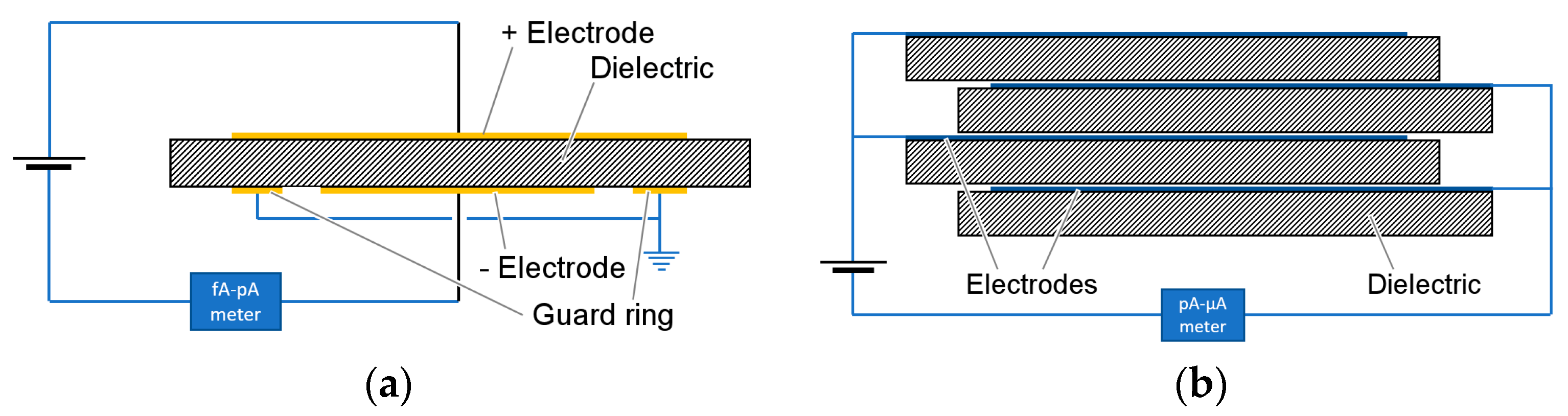
When testing thick dielectrics, it is common practice to use a three-electrode system, as depicted in
Figure 10a, where, in addition to positive and negative electrodes, a third guard ring electrode is introduced to block surface conduction. With ultra-thin films, the guard ring may be redundant because of the relatively low voltage of the test and the consequent mitigation of surface conduction processes; nevertheless, it is often retained, as good practice. Typical film capacitors adopt a simpler two-electrode construction, as depicted in
Figure 10b, where the guard ring is not used, and electrical separation of the two polarities relies on a sufficiently large portion of film being left unmetallized, the so-called free margin.
With micron-sized polypropylene films and centimeter-sized electrodes, the leakage current is expected to fall in the range of 10−9–10−12 A, even at the highest temperature and electric field stress conditions. For this reason, specific femto-ammeters (i.e., with sensitivity below 10 pA) are necessary for proper measurement.
Wound film capacitors can be used in place of film coupons, and several recent characterization works have been performed based on this sample type [
43,
56]. In many cases, the electrode metals are not disclosed, but it is possible to assume that single-sided aluminum/zinc metallization was used, in accordance with the standard practice in film capacitor manufacturing [
57]. With this approach, the electrode surface is in the range of 1–10 m
2, so LC is expected to be several orders of magnitude higher than with coupons, and it is measurable with simpler equipment. On the other hand, this approach requires the film sample to be available in quantities that are sufficient for the metallization and winding of capacitors on mass-production or pilot machines, which may not be possible during the early stages of research on materials. These two approaches are complementary: testing film coupons is preferable for screening dielectric materials or film modification processes, while testing finished capacitors allows the comparison of products or manufacturing processes in real-world applications.
Temperature and voltage must be constant in DC conductivity experiments, so specific chambers and power supplies are employed to keep variability and oscillations at acceptable levels. Voltage must be free from high-frequency noise (ripple) that would transfer to the current measurement and reduce the actual sensitivity of the ammeter.
Because of the inevitable polarization and absorption transient currents, measurement of the steady-state conduction current requires extremely long test times. Most of the reviewed works utilize stabilization times close to 104 s, with some extending to 106 s. The proper conditioning of samples is usually reported, with a common condition being 24 h at the test temperature with electrodes short circuited to ground. With long experiments, it seems advisable to have a stabilization time that is longer than the test time, in a chemically inert environment, so that further thermal modification during the test can be neglected.
The long stabilization time required to reach a steady state is often undesirable, so few works accept a time that is 103 s or shorter as a sufficient stabilization period, with presumable overestimation of the conductivity value. Other works propose alternative solutions to overcome the long stabilization time after application of voltage, as follows:
Use of the same sample for consecutive measurements, at increasing applied field [
51,
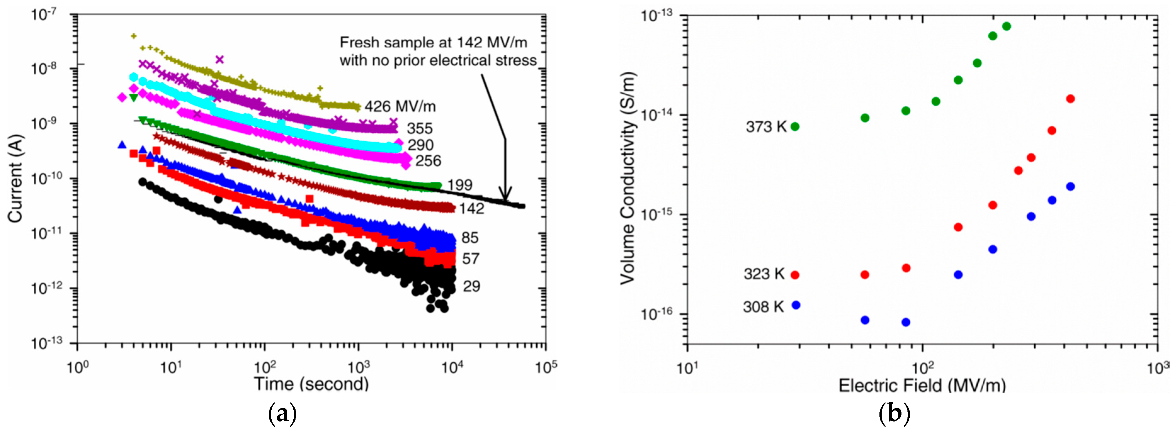
58]. Each measurement step acts as a pre-treatment and stabilization step for the following ones. This method is applicable for the comparative characterization of samples if the procedure is repeated identically every time. Because each measurement step represents a pre-conditioning phase for the following measurements, all steps will end up having different stabilization times, with possible overestimation of conductivity in the initial ones with the lowest preconditioning times. The results obtained by Ho using this method and the deviations at low field are reported in
Figure 11.
Subtraction of the unwanted non-steady-state components of the conduction current from the measurements to obtain the constant background conduction value. Setups for fast conduction current measurement have been proposed on the basis of the application of the electric field as an ascending ramp with superimposed low-voltage AC [
32].
Measurement of steady-state current at high temperature followed by a temperature scan at constant voltage [
33]. This method showed results comparable with steady-state conductivity on epoxy resin substrates. Verification of this method on polypropylene resulted in the under- or overestimation of conductivity, depending on the cooling conditions [
34], due to the existence of concurrent temperature- and time-dependent mechanisms.
The diversity of the setup and experimental procedures will be reflected in the results and interpretation of the conduction mechanism. Despite it being expected that substrates will be similar, it is rare to find agreement in published characterization data.
9. Review of Published Data
The literature on the conduction and reliability of BOPP capacitor films at high field is vast, but is mostly focused on relatively high film thicknesses, generally from 6 µm to 25 µm. No literature was found by the authors investigating ultra-thin BOPP (2–4 µm), or for film thickness below 5 µm in general. A few works have reported the characterization of sub-micron films, but in these cases, films were obtained either by evaporation or solvent casting, so they cannot be considered representative of biaxially oriented film.
The principal characterization works were evaluated and compared, focusing on those in which the tests covered the reference condition of 105 °C and 250 V/μm. The main contributions to the subject will be briefly summarized and discussed, and the conductivity data obtained will be compared.
DasGupta reported extensive conduction measurements for metallized polypropylene [
59] in the temperature range −193 °C to 100 °C, and an electric field up to about 100 V/µm. Polarization curves show that a steady state was reached only for T > 340 K at times t > 10
4 s. The conduction mechanism identified in this work was hopping (
Hi) for conditions above 100 °C, with no dependency on the electrode material (Au, Al, In) or thickness (9.5 µm to 36 µm).
Ho studied the conduction of small sheets (3 cm
2) of Au-metallized 7 µm BOPP film in the temperature range 35 °C to 100 °C under a field of 29 V/µm to 430 V/µm [
58]. Samples were preconditioned by 24 h annealing at 70 °C with shorted electrodes. Ho concluded that conduction occurred via a hopping (
ionic) mechanism with a jump distance between 1.4 nm and 3.5 nm. Schottky emission and the Poole–Frenkel effect were also considered, with good fit of experimental data, but they were excluded because fit required a relative dielectric constant that was too high (ε
r > 15).
Ikezaki studied the conduction of BOPP in relation to crystallinity and the thermal history of the samples [
60]. The area of the samples was 3.14 cm
2, with thickness in the range 10–40 μm and an electric field up to 40 V/µm. Tests were conducted at 72 °C to avoid changes in the crystallinity of the samples during the test. Schottky, Poole–Frenkel and SCLC mechanisms were excluded because of the poor fit of the experimental data, and hopping (ionic) conduction was identified as the best fitting mechanism. The results for the jump distance were in the range 4–10 nm, with higher-crystallinity film exhibiting lower jump distance. Interestingly, at low electric field, Ikezaki measured higher conductivity for more crystalline film, while at high field, the trend was reversed.
Crystallization was also studied by Ran et al. [
61] under similar stress conditions: 30 V/µm and 85 °C. The resulting conductivity was always inversely proportional to crystallinity, and the authors suggested that conduction took place preferentially in the amorphous regions.
Kahouli reported the full characterization of two kinds of commercially available, capacitor-grade, 11.8 µm polypropylene film [
62]. The identified conduction mechanism was hopping, with the introduction of a secondary ionic conduction mechanism to explain the high-temperature results. Films with higher crystallinity were found to have lower conductivity, which is in agreement with other authors, and based on the calculated hopping distance, it was suggested that conduction took place preferentially in the amorphous region.
Li reported the steady-state conduction of capacitors made with 7.5 µm thick metallized BOPP under an electric field up to 500 V/µm. Leakage current was measured across a resistor mounted in series with the capacitor under test [
43]. Steady-state currents were measured after 24 h of polarization. Li concluded that the data fit could be either Schottky emission or hopping conduction. The correlation with film crystallinity was confirmed, with higher crystallinity leading to lower conductivity. In a subsequent work on polypropylene [
56], Li proposed a modified Poole–Frenkel model for better data fit, based on the previous work of Ieda [
42]. The equation included a jump distance parameter similar to that in the ion-hopping mechanism. The calculated jump distance and the relative dielectric constant were 0.6 nm and 15, respectively, similar to what had previously been reported by Ho.
Karanja suggested that conduction was not intrinsic, but rather caused by contaminants. The conduction current was reduced after washing the samples in hexane [
63]. The tests were performed on 35 μm PP films, in the temperature range 50–110 °C, with steady-state conductivity recorded after 1000 s. Several conduction models were considered, but the best fit was obtained with hopping conduction (ionic) and a 6 nm jump distance.
Zhao reported measurements on 5.8 µm BOPP in the range 200–450 V/µm, concluding that the dominating mechanism of conduction was space-charge-limited conduction (SCLC) [
64]. Measurements were taken after 600 s of polarization, so the model described here may not be comparable with other works in which steady-state conduction was measured after a longer stabilization time. Temperature was not indicated, so room temperature was presumed.
Wu compared several capacitor-grade high-temperature dielectrics with BOPP up to 450 V/µm, finding that polypropylene exhibited the lowest conductivity at 100 °C and high electric field [
65]. The mechanism was identified as ion hopping for all polymers under test.
Ghorbani reported conduction measurements on 8.3 µm, 10 µm and 15.2 µm thick polypropylene films, focusing on the conduction current decay over time, and the lack of proper stabilization even with test times in excess of 10
6 s [
13]. The electric field was up to 200 V/µm. The steady-state conductivity was not determined, because it was not visible within the duration of the experiment, and it was assumed to be lower than 10
−16 S/m. A local maximum was found in all conduction curves, and attributed to the time-of-flight of the charge carriers passing through the dielectric thickness. The peak position on the time coordinate was proportional to the applied field, similarly to what was reported by Fischer about oxidized polyethylene [
66].
Ritamaki, in a recent paper, described the characterization of 5 µm and 10 µm BOPP films by means of conductivity measurements, among other techniques (thermally stimulated depolarization currents, small and large area breakdown) [
51]. The samples were metallized with either nickel/gold or aluminum, and the testing conditions were up to 100 °C and 250 V/µm. It was suggested that the conductivity decay was dependent on a thermally activated crystallization of the amorphous phase and, because the long-term value of the conduction current appeared to be independent from the electric field, the major conduction mechanisms were disregarded in favor of a space charge (SC)-related mechanism. The effect of the electrode material was also explored, with Al-metallized samples showing considerably higher conductivity than Ni/Au samples.
On a separate level, Ochiai [
67] and Zheng [
68] extended the study of polypropylene to extremely thin substrates: the former studied 6–8 nm thick PP evaporated on glass at fields of up to 1200 V/µm, and the latter worked with 140 nm films obtained by high-temperature spin coating and subsequent annealing, tested up to 550 V/μm. In both cases, hopping was identified as the dominating conduction mechanism, at least in a certain range of electric field, with tunneling becoming a better fit at the highest electric fields.
Literature results referring to the stress conditions of interest are reported in
Table 1. The reported values are relative to the reference conditions of 105 °C and 250 V/µm and were obtained through interpolation or extrapolation of provided data. Works reporting conductivity at lower electric field are listed in
Table 2, with reference conditions of 105 °C and 30 V/µm.
Based on the reviewed papers, conduction in BOPP at high temperature and high electric field was identified by most of the authors as being hopping conduction, with the ion hopping equation being used to fit the experimental data. The hopping distance and activation energies are rarely in agreement, with deviations between different works being greater than one order of magnitude. The hopping distance calculated by different authors ranges from 0.15 nm to over 10 nm, with both minimum and maximum values appearing not to be compatible with the physical structure of polypropylene and the distribution of traps in the lattice. The conductivity value under the target conditions varies by almost five orders of magnitude, with higher conductivity generally being found in shorter experiments, indicating that stabilization time plays a significant role in the measurements.
10. Conclusions
While the literature on thick-film plastic dielectrics is vast, only a few authors have studied polypropylene in the 1–10 µm thickness range under high electric field and at high temperatures of interest. In particular, no publications were found focusing on the thickness range from 2 to 4 µm, which is the most relevant for modern DC-link capacitor applications. The existing literature provides useful background for the further extension of characterization to thinner-gauge films, the main takeaway points of which can be summarized as follows:
The conductivity of thin BOPP film, considering the reference conditions of 105 °C and 250 V/µm, was found to be in the range of 10−12–10−14 S/m. Works in which long stabilization times were used (24 h and more) generally report conductivity values of around 10−16 S/m, suggesting that the duration of measurement plays a substantial role, as a steady-state condition may not be reached in a shorter time.
Hopping is identified as the main conduction mechanism in BOPP under a high electric field, with the ion-hopping equation being used for fitting the experimental data. Descriptive parameters such as the trap distance and energy barrier height are rarely in agreement between the evaluated works. A possible cause for this is related to the procedure and sample history. Recent evaluations suggest that crystal structure, roughness, thermal history, and chemical ageing play a relevant role, so they should either be included in the model together with the intrinsic characteristics of the material, or reported for reference purposes.
Localized energy states or charge traps are considered in all conduction mechanisms to explain the dependency of conductivity from the electrical and thermal stress applied to the material. Usually, single-energy-level trap models are used to fit the experimental data, and the nature of traps is not clarified. A deeper characterization of the material might be accessible via thermally or photo-stimulated depolarization methods for the determination of the trap levels. Experimental data fit requires computational modeling of the dielectric in place of single equations.
The role of the electrode material and the electrode/dielectric interface on injection and extraction of charge carriers has been studied by a few authors, with variable results. Studies focusing on similar dielectrics [
71,
72] attribute high relevance to the metallization, as it determines the injection and extraction dynamics and consequently the actual electric field distribution inside the sample throughout the polarization.
The effect of charge injection and the consequently inhomogeneous electric field within the dielectric are generally not considered by conduction models, while they are considered in computational works relating to space charge. In the presence of substantial field distortion within the material below, the “real” conductivity of the material would not be accessible with the simple models normally used.
Recent works have drawn attention to the fact that under several conditions, a proper steady state is never reached. Tests with durations greater than 106 s have been presented, showing no sign of stabilization or change in decay trend. Similar considerations could be extended to the data presented in many of the reviewed works, in which the steady state is not clearly visible within the experiment time. These considerations suggest that the standard conduction models are not suitable for describing the observed current flow trend and may require opening to a novel interpretation of the conduction mechanisms in the plastic materials.


