1. Introduction
Multijunction semiconductor structures are used in photovoltaics to absorb the solar spectrum among materials with differing bandgaps in order to convert it more efficiently to electrical power [
1]. Direct bandgap materials such as III-V semiconductors are better suited for this purpose because of their high absorbance and low non-radiative recombination rates. Due to constraints on lattice-matching during epitaxy and the high cost of III-V substrates, the most commercially successful multijunction solar cell concept has been the InGaP/GaAs/Ge triple-junction [
1,
2] shown on
Figure 1. However, this technology is almost only used for applications where efficiency is of primary importance relative to the cost, such as in space energy systems. For terrestrial applications, the high cost of III-V multijunction solar cells means that they must be integrated into tracking systems with concentrator optics in order to reduce the area of solar cells in proportion to the concentration factor and the associated increase in efficiency. III-V concentrator photovoltaics cannot yet compete with Si flat panel solar cells which dominate the market due to much lower costs offsetting their lower efficiency.
Various strategies are currently researched in order to reduce the cost of III-V solar cells for concentrator photovoltaics systems, such as Ge substrate reuse [
3,
4] or integration on Si [
5], for example. After epitaxy, one of the major costs during the fabrication of III-V solar cells is the front contact metallization [
2]. Several variations of the metallization and/or metal deposition technique have been studied in order to reduce this cost [
6,
7,
8,
9]. In particular, it was shown that the standard AuGe/Ni/Au front ohmic contact metallization could be replaced by a thin Pd/Ge/Ti/Pd stack combined with a thick Al layer [
9]. It was estimated that the cost of the new metallization scheme is 6.3% of AuGe/Ni/Au contacts [
9]. Furthermore, the specific contact and bulk resistivities could be lowered by an order of magnitude, which allows for operation at higher concentration factors.
Increasing conversion efficiency can potentially help reduce the end cost of the generated power. The most common way to increase efficiency is by adding more subcells [
1,
2]. However, this comes with an important rise in manufacturing costs [
2] and limits operation due to variations in the solar spectrum over time and the necessity for more precise solar system optics [
10,
11]. For silicon technology, one strategy to improve efficiency has been the replacement of diffused ohmic contacts by passivated contacts to form metal/semiconductor or metal/dielectric/semiconductor interfaces [
12,
13,
14,
15]. As shown in
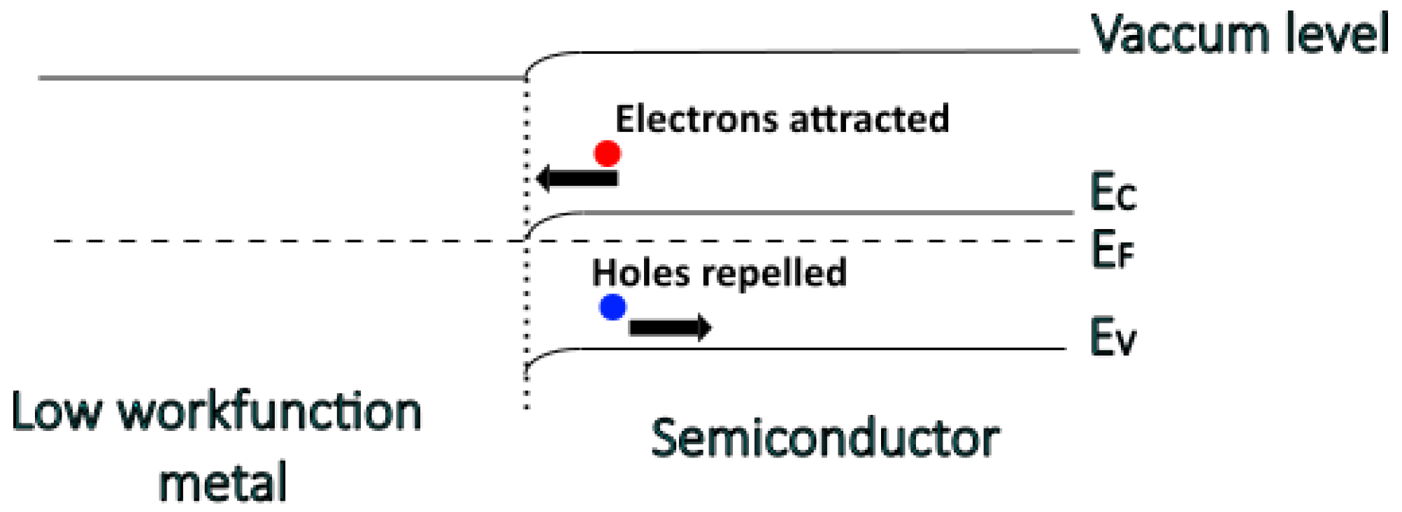
Figure 2, using a metal with a low work function on an n-type semiconductor creates a barrier for holes. This can help reduce recombinations at the contacts and increase the open-circuit voltage. Applying this concept to III-V multijunction solar cells could potentially provide similar improvements and reduce cell manufacturing costs. In the present work, we apply this strategy to fabricate III-V/Ge triple-junction solar cells using only Al as the front contact metallization. We demonstrate that this low-cost metallization might improve photovoltaic performances in low-light conditions such as in aerospatial energy systems and could also be suitable for high-light concentration terrestrial applications.
2. Materials and Methods
Multijunction solar cells with an active area of 2 × 2 mm
were fabricated on samples from an InGaP/(In)GaAs/Ge monolithic heterostructure wafer. The top layers and intended metallization are shown in
Figure 3. The samples were first cleaned in acetone, IPA, rinsed in deionized water, and dried with N
. On some of the samples, the GaAs contact layer was etched with an NH
4OH:H
2O:H
2O
2 (3:80:3) solution (interface on AlInP window). A subset of samples was passivated by immersing them in (NH
4)
2S
x for 20 min at 65 °C. A diluted solution (2% in water) was used as it was observed that the window layer was etched by the concentrated solution. Sulfur passivated samples were subsequently annealed in N
2 for 1 min at 250 °C to sublimate the excess sulfur. The front contact metallization was defined by photolithography in order to lift off a 1 μm Al layer, which was deposited by e-beam evaporation. A reference sample was obtained with the same process except for sulfur passivation and a Pd/Ge/Ti/Pd stack (50 nm/100 nm/50 nm/50 nm) ohmic contact was evaporated on the contact layer before depositing 1 μm Al, as proposed by P. Huo et al. [
9]. Deoxidation with a buffered oxide etch solution (BOE) was performed prior to metal deposition on samples that were not passivated with (NH
4)
2S
x. The front surface was protected with resist, the Ge back surface was deoxidated with BOE and Ni was evaporated on it. Samples were then singulated by saw dicing, the front surface protection resist was removed, and the samples were immersed for 1 min in NH
4OH:H
2O:H
2O
2 (3:80:3) to passivate perimeter defects caused by saw dicing and pattern the GaAs contact layer in cases where it was not already etched. An SiN
x/SiO
x (51 nm/48 nm) anti-reflection coating was then deposited by PECVD at 300 °C. Photolithography and etching by CF
4 inductively coupled plasma were performed to remove the dielectric coating in the busbars region.
J–V characteristics were obtained under AM 1.5 D spectrum at 1 sun intensity using a Newport Oriel Sol1A™class ABB solar simulator and are recorded with a Keithley 2602A source-measurement unit. High light intensity characterization was performed in a Sinton instrument HCCT-350 flash tester up to a concentration factor of 900 suns. Dark current measurements were obtained with a Keithley 4200 SCS unit and were performed on 200 × 200 square contacts to avoid current crowding effects. All measurements were performed at 25 °C.
3. Results and Discussion
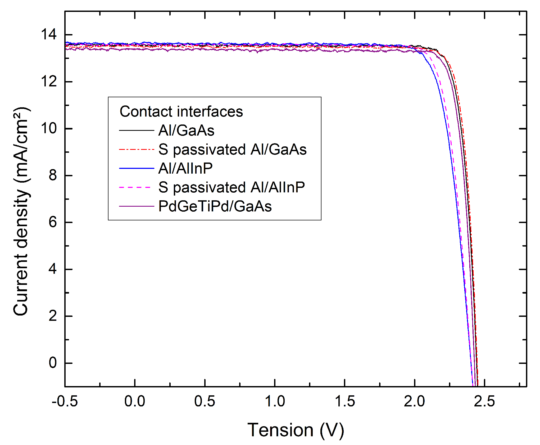
The J–V characteristics of the various solar cells under 1 sun illumination are shown in
Figure 4. The short-circuit current density (J
), open circuit voltage (V
), and fill factor are summarized in
Table 1. The flatness of the curves in the low voltage region indicates a high shunt resistance. The J
values are in line with expectations for the epitaxial structure considered here. It also shows that the anti-reflection coating design was adequate and that chemical processing, in particular, with the ammonium sulfide solution, did not degrade the top window layer. Solar cells for which Al was deposited on AlInP show a slightly reduced V
and fill factor compared to the reference sample with Pd/Ge/Ti/Pd ohmic contacts. They exhibit a high series resistance, which can be seen from the lower slope when approaching V
. To the contrary, the fill factor for the samples obtained by deposition of Al on the GaAs contact layer is similar to the reference sample at around 87%. Furthermore, the Al/GaAs interface samples show a slightly higher V
by 18–19 mV compared to the reference cell, without and with sulfur passivation. This indicates that passivated contacts are effective in reducing electron-hole recombinations at the metal/semiconductor interface. This result is an indication of the potential of passivated Al contacts to improve III-V multijunction solar cell performances, at least in relatively low light exposure, such as in the case of aerospatial energy systems.
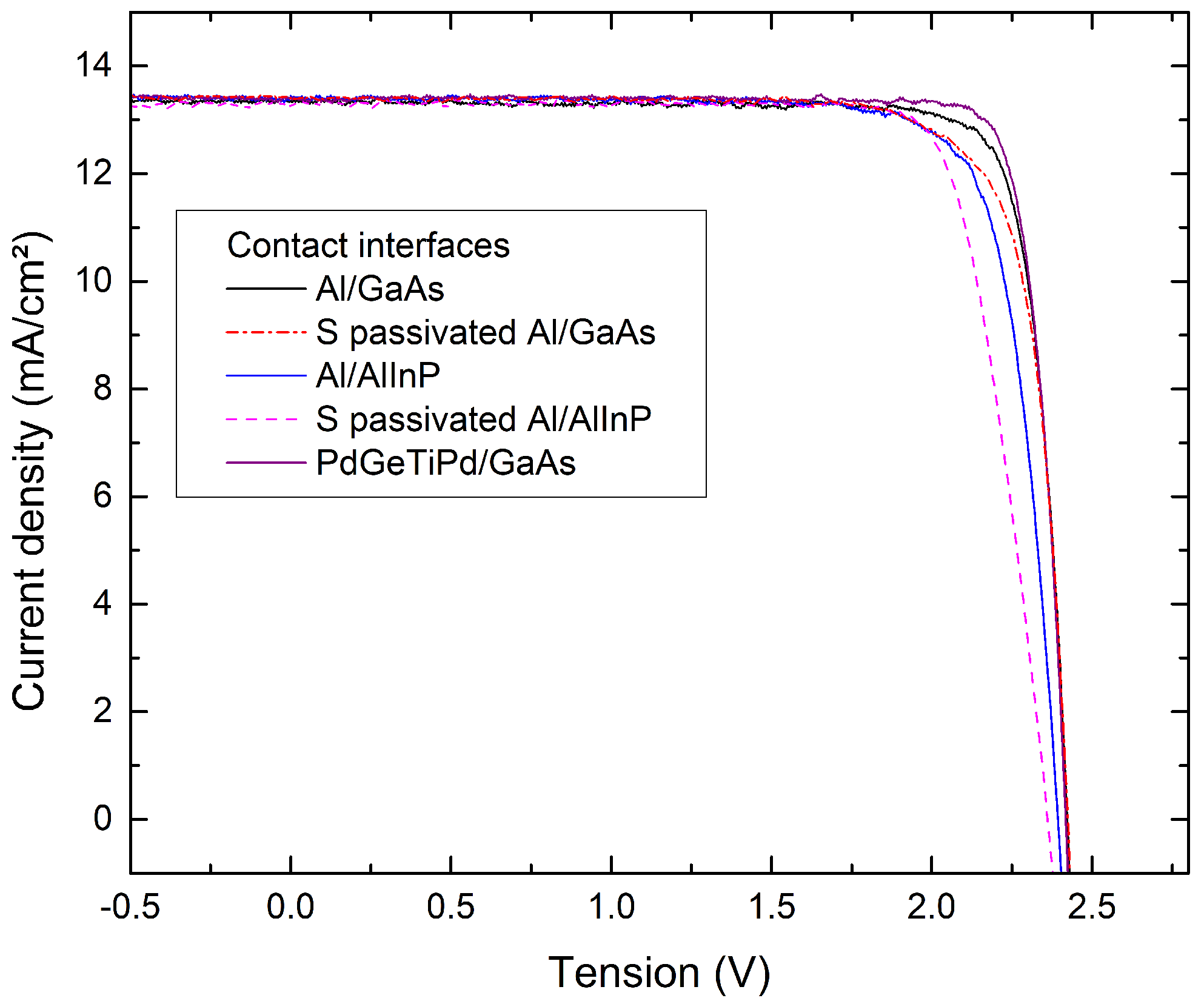
Figure 5 shows the dark current characteristics measured by sweeping the voltage back and forth for the different interfaces. This measurement was performed on 200 μm × 200 μm diodes (full surface, no grid). There is a strong reduction of the increase of current at high voltage, which is due to a series resistance-dominated behavior in that region. The effect of series resistance is more prevalent for samples with passivated contacts. The characteristics of samples with passivated contacts also show a shift of the voltage point at which the current is minimal in cases where sulfur treatment was not applied. This indicates that a dielectric layer constituted of native oxides could still be present at the interface and lead to electron capture during the forward sweep. The reverse saturation current densities were estimated by exponential fitting and projection towards the voltage where the current is minimal (to account for dielectric charging). For passivated contact interfaces, it varies from 1.1 × 10
to 3.0 × 10
A/cm
2 while it is 2.6 × 10
A/cm
2 for the reference sample. Passivated contacts have a lower reverse saturation current by an order of magnitude. This indicates that the implemented passivated contacts effectively reduced recombinations near the metal/semiconductor interface.
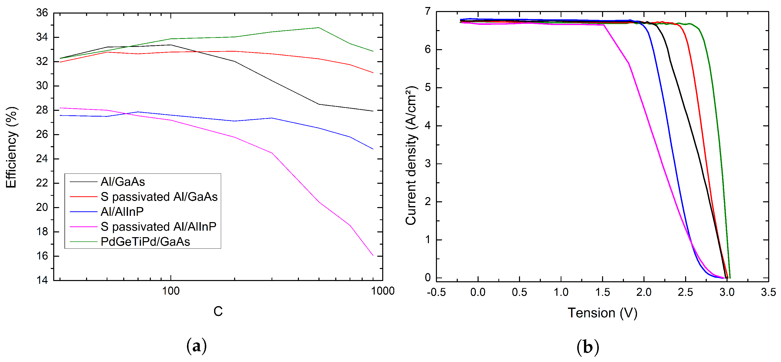
The efficiency as a function of the concentration factor is shown in
Figure 6a. For Al/AlInP interfaces, the efficiency is generally lower with a maximum of 28% and only decreases with the concentration factor. This is especially marked when sulfur passivation is performed and results in a very high series resistance. For Al/GaAs interfaces, there is an increase of efficiency with concentration up to 32–33% until around 100 suns, showing a lower series resistance. This is followed by a degradation of efficiency for higher concentration factors. With sulfur treatment, the curve is broader, the degradation is less pronounced, and this sample, therefore, has the lowest series resistance among samples with passivated contacts. However, the reference sample is less impacted by series resistance, with a maximum efficiency around 34.6% at 500 suns.
Figure 6b shows the J-V characteristics obtained under a concentration factor of 500 suns. A marked S-shape appears for devices with Al deposited on the AlInP window layer, which degrades the fill factor, explaining the low efficiency. This is a common behavior that is often seen on Si solar cells with metal/dielectric/semiconductor contacts and this appears due to a high Schottky barrier or a dielectric interfacial layer that is too thick [
12,
16]. It is also more likely to be present for high photogenerated current densities, which explains why it was not seen on the J-V curves at a 1 sun intensity. This behavior is absent when Al is deposited on the GaAs contact layer but the J-V characteristics confirm a higher contact resistance than for the Pd/Ge/Ti/Pd ohmic contacts. However, sulfur passivation at the Al/GaAs interface does reduce resistive losses significantly. Although at this point, the performances under concentrated light of the Al/GaAs contacted solar cells are inferior compared to the reference sample, these results indicate that passivated contacts could potentially be applicable in concentrator systems, especially when combined with the sulfur passivation treatment.
The impact of annealing samples with passivated contacts was investigated by using a rapid thermal annealing system at 370 °C for 1 min in N
2. Note that transmission-line measurements (not shown here) indicate that passivated contacts still present a Schottky behavior. The 1 sun J–V characteristics are shown in
Figure 7 and their main parameters are summarized in
Table 2. In all cases, the J
remained stable after annealing, but a slight decrease of V
and fill factor is observed. For the Al/AlInP interface, the reductions in V
are 17 mV and 48 mV with and without sulfur treatment, respectively. For the Al/GaAs interface, the V
degradation is similar whether the sulfur treatment is applied or not and is at 22–23 mV. However, the V
for the Al/GaAs interface remains at a level similar to the reference sample.
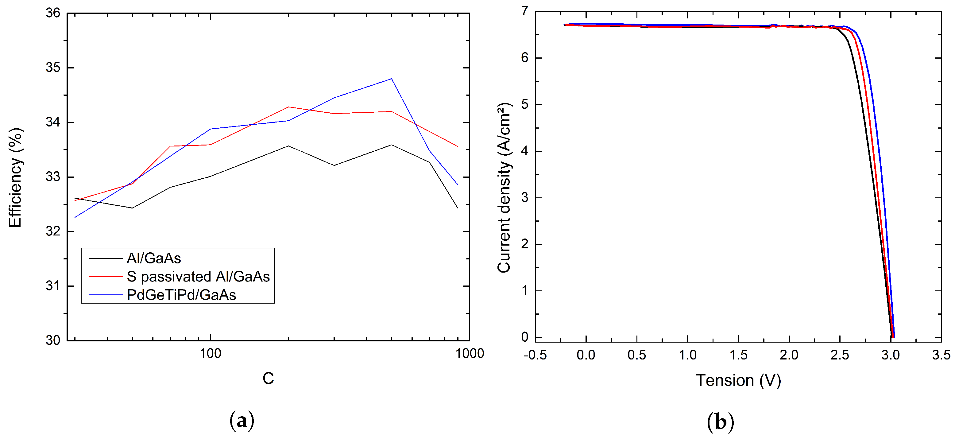
Figure 8a shows the comparison of efficiency under concentrated light between annealed Al/GaAs contact interface samples and the reference solar cell. The peaks in efficiency for passivated contact samples occur at a much higher concentration factor (near 500 suns) than before annealing. The maximum efficiencies also increased to around 34.2% and 33.6% with and without sulfur treatment, respectively.
Figure 8b shows again the absence of an S-shape in the J-V characteristics under concentration. An important reduction of series resistance losses is observed compared to what was shown before annealing and the performances are almost the same as for ohmic contacts. This demonstrates that the thermal treatment was effective in reducing contact resistance and that it is possible to obtain conversion efficiencies under high light intensity similar to the Pd/Ge/Ti/Pd ohmic contacts with a simple Al metallization.
The objective of applying metal/semiconductor passivated front contacts on III-V multijunction solar cells to improve V
was achieved even if only a small increase of V
was observed under 1 sun illumination. Further work is needed to improve this concept in order to obtain a more significant gain in V
, particularly under concentrated light. From the economical point of view, this technology is very interesting for industrial production as using only Al for the front contact metallization is much cheaper than ohmic contact metal stacks comprising precious metals.
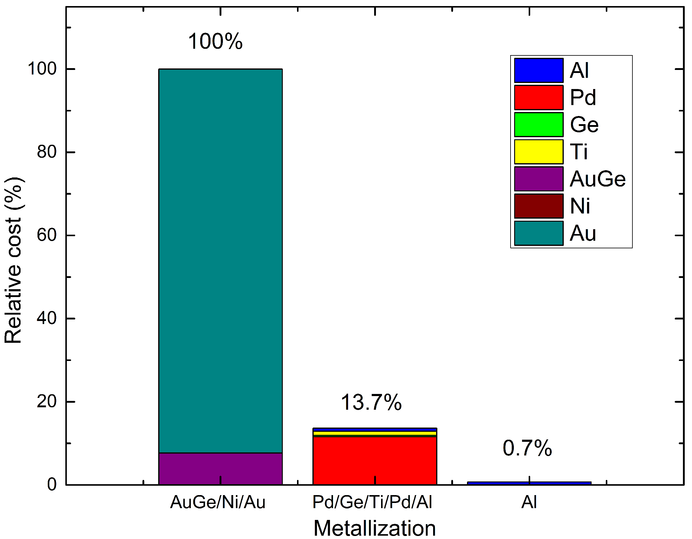
Figure 9 compares the relative costs of e-beam evaporated materials used in AuGe/Ni/Au and Pd/Ge/Ti/Pd/Al ohmic metal stacks and the Al passivated contacts in a manner similar to the estimates given in reference [
9]. This estimate is based on current low volume prices from our supplier (Kurt J. Lesker Canada, Inc., Jefferson Hills, PA, USA) and is subject to important variations due to the volatility in the precious metals market. Removing Au by going from the AuGe/Ni/Au stack to the Pd/Ge/Ti/Pd/Al stack already allows for a material cost reduction of more than 86%. However, with Al-only passivated contacts, the cost is nearly 20 times lower than Pd/Ge/Ti/Pd/Al ohmic contacts, which is largely because Pd is not used. Even though the fabrication process may add (NH
4)
2S
x passivation and supplementary annealing, the costs associated with these steps should be largely offset by material savings in an industrial scale production. Other economical advantages of simplifying the front contact metal stack are also difficult to quantify, such as the reduction of the number of crucibles managed, lower operator time involvement in the process, and potentially better process stability and reproducibility.


 ,
, 


