Article

Real-Time ITO Layer Thickness for Solar Cells Using Deep Learning and Optical Interference Phenomena

1
Interdisciplinary Program in Photovoltaic System Engineering, Sungkyunkwan University, Suwon 16419, Republic of Korea
2
College of Computing and Informatics, Sungkyunkwan University, Suwon 16419, Republic of Korea
3
Department of Electrical and Computer Engineering, Sungkyunkwan University, Suwon 16419, Republic of Korea
4
College of Information and Communication Engineering, Sungkyunkwan University, Suwon 16419, Republic of Korea
*
Authors to whom correspondence should be addressed.
The authors contributed equally to this work.
Energies 2023, 16(16), 6049; https://doi.org/10.3390/en16166049
Submission received: 9 June 2023 / Revised: 11 August 2023 / Accepted: 16 August 2023 / Published: 18 August 2023
(This article belongs to the Section A2: Solar Energy and Photovoltaic Systems)

Abstract

:
The thickness of the indium tin oxide (ITO) layer is a critical parameter affecting the performance of solar cells. Traditional measurement methods require sample collection, leading to manufacturing interruptions and potential quality issues. In this paper, we propose a real-time, non-contact approach using deep learning and optical interference phenomena to estimate the thickness of ITO layers in solar cells. We develop a convolutional neural network (CNN) model that processes microscopic images of solar cells and predicts the ITO layer thickness. In addition, mean absolute error (MAE) and mean squared error (MSE) loss functions are combined to train the model. Experimental results demonstrate the effectiveness of our approach in accurately estimating the ITO layer thickness. The integration of computer vision and deep learning techniques provides a valuable tool for non-destructive testing and quality control in the manufacturing of solar cells. The loss of the model after training is reduced to 0.83, and the slope of the test value in the scatter plot with the true value of the ellipsometer is approximately equal to 1, indicating the high reliability of the model.

1. Introduction

Solar cells have arisen as an important topic of research in the field of environmentally friendly energy conversion as a result of the increased use of renewable energy [1,2,3,4,5,6,7,8,9]. The thickness of the indium tin oxide (ITO) layer, a typical transparent conductive oxide (TCO) layer, has a significant impact on solar cell performance [10,11,12,13,14,15,16,17]. However, traditional measurement methods, such as ellipsometer measurements, frequently necessitate the interruption of manufacturing processes to collect sufficient samples [18,19]. This interruption not only reduces manufacturing efficiency but may also have an impact on the conductive layer’s quality. As a result, developing a real-time, non-contact approach for detecting the thickness of the conductive layer during production has enormous practical and scientific importance.
Numerous studies have delved into the application of machine vision techniques and deep learning for assessing the various attributes of objects [20,21,22,23,24,25]. Deep learning has been used in picture categorization and object detection in a substantial number of these studies. Nonetheless, deep learning models for forecasting continuous variables, such as the thickness of conductive layers, are still in short supply. Our research is conducted within this framework, aiming to introduce a novel, deep learning-driven approach for estimating the thickness of the transparent conductive oxide layers in solar cells.
Our most significant contribution is the advent of an image-based technique to predict ITO layer thickness. This technology employs deep learning algorithms and enables real-time estimation without interfering with the production process. We carefully designed and implemented this model, establishing its efficacy through experimental validation. In comparison with common thickness measurements such as stylus profilometers, atomic force microscopy, cross-section scanning electron microscopy (SEM), transmission electron microscopy (TEM), and ellipsometry, which require complex sample preparation and/or likely result in some errors due to direct friction contact, the proposed method is a simple, fast, real-time, and non-invasive approach that reduces the risk of cell damage and ensures the integrity of the cells. Thus, it is an approach to be favored by industrial production processes.
The field of material science has greatly benefited from the integration of computer vision technologies, which have become an indispensable tool for characterizing material surfaces. Due to its capacity to handle large volumes of microscopic images, computer vision is increasingly replacing traditional imaging technologies, offering a more precise and efficient analysis. Wang and his team [26], for instance, designed a computer vision-based machine learning method for identifying fatigue crack initiation sites. This was a groundbreaking study as it pioneered the use of machine learning techniques for automating the detection of minute defects that could potentially lead to structural failures. By leveraging computer vision, they were able to analyze images of materials to detect early signs of stress and strain that could eventually result in a crack. This has profound implications for preventive maintenance in various industries where the early detection of fatigue cracks can help prevent catastrophic failures. Similarly, Gabriel and colleagues utilized computer vision algorithms for the micro-morphological analysis of cut marks to identify stone tooling materials [27]. This application of computer vision has provided a more objective and quantifiable approach to archaeological research. Instead of relying on human observation, which can be subjective and error-prone, their approach automated the process, reducing human bias and significantly increasing the speed and accuracy of material identification. Karthikeyan et al. [28] pioneered the application of artificial neural networks for surface roughness evaluation using computer vision. Surface roughness is a critical parameter in many manufacturing processes, affecting both the aesthetic and functional characteristics of a product. Traditionally, surface roughness is measured using tactile methods, which can be slow and may potentially damage the surface. Karthikeyan and his team demonstrated that computer vision combined with artificial neural networks can provide a non-contact, fast, and accurate alternative for assessing surface roughness.
These pioneering studies underscore the immense potential of computer vision in various domains, from preventive maintenance and archaeology to manufacturing. By integrating computer vision with machine learning techniques, researchers are not only able to process and analyze images more efficiently but also make predictions and decisions that are critical to their respective fields. This has paved the way for more innovative applications, such as the one proposed in this paper: estimating the thickness of the transparent conductive oxide layer in solar cells using deep learning.

2. Materials and Methods

As shown in Figure 1, the experiment includes two processes: data selection and defining the model architecture. Our proposed code and dataset are now available at: https://github.com/zots0127/ITO-thickness, accessed on 8 June 2023.
We used 50 samples of different thicknesses to collect data and expanded the data to 500 by an image augmentation method. We randomly divided these 500 samples into a training set and a test set, where 80% of the samples were used for training and the remaining 20% of the samples were used for testing. Because our method fits the data in a stationary environment, only a small amount of evenly distributed data are needed to fit the entire thickness range at a time.
Dataset Details: Our dataset consists of samples in the 30–160 nm thickness range, with the majority centered between 80 and 160 nm and a few located between 30 and 40 nm. These samples were collected in bulk in a variety of environments and multiple batches were collected. After taking photographs, we captured images from the center of the samples for the dataset.
Camera specifications: A Sony A7R4 camera, with a resolution of 9506 × 6336, and a Sony 135 mm/F1.8 GM lens, totaling 61 MP, were used in our experiments. We also tested the performance using an IMX713 sensor and a 77 mm/F2.8 lens with a resolution of 12 MP.
Shooting Settings and Conditions: There were no other light sources in our environment at the time of shooting. We used a 15 W LED fill light with a power setting of 30% and fixed the distance to the sample.

2.1. Experiment Principle

The underlying principle of our experiment is grounded in the optical interference phenomenon, which is the primary determinant of color variation in ITO films as a function of thickness [29,30]. Optical interference, a fundamental property of light, occurs when waves of light combine to form a resultant wave of greater, lower, or the same amplitude [31]. This effect is most pronounced when light interacts with thin films, such as those made of ITO.
Because light interference is created by the fluctuating nature of light, which happens as light waves travel through the film, causing the light of a given wavelength to be boosted or lessened and thereby changing the reflected light, the color change of ITO films impacts light interference [32,33].
As shown in Figure 2a,b, an electromagnetic wave emitted by a monochromatic point source S is incident on a transparent parallel plane plate. The top surface of the parallel plate experiences reflection and refraction; the refracted light is then reflected by the lower surface, which then reflects the light, which is then refracted by the upper surface into the original medium. This refracted light will certainly coincide with another reflected light directly reflected by the upper surface at a certain point in space, and since they are both part of the electromagnetic wave emitted from the same source, they are coherent light, which will then form non-fixed interference fringes (Figure 2b) [34,35]. If the light source is an extended light source, the visibility of the interference fringe will be reduced in general, but if we consider the case where the two reflected lights are parallel, i.e., the point of coincidence is at infinity, then a fixed-domain isotropic interference fringe will be formed (Figure 2a). According to the geometric relationship, the optical range difference between the two beams can be expressed as:
Δ L = n 2 AB ¯ + BC ¯ n 1 AN ¯
where n2 is the refractive index of the parallel plane plate and n1 is the refractive index of the surrounding medium. The specific length can be expressed as:
AB ¯ = BC ¯ = d cos θ
AN ¯ = AC ¯ sin θ
where d is the thickness of the parallel plane plate, and θ is the angle of incidence and θ’ is the angle of refraction, both of which satisfy the law of refraction. The optical range difference and phase difference thus obtained are:
Δ L = 2 n 2 d cos θ
δ = 4 π λ n 2 d cos θ
Furthermore, taking into account the reflected phase transition on the higher or lower surface, the phase difference should be:
δ = 4 π λ n 2 d cos θ ± π
The interference conditions are:
2 n 2 d cos θ ± λ 2 = m λ
where m is the order of interference (generally taken as 1 for first order) and λ is the wavelength of light. If the two surfaces of the parallel plane plate in isotropic interference are not strictly parallel, as shown in the figure, then for the incident light from a monochromatic point source S, the reflected light from its upper and lower surfaces will always form interference at a point P in space, and its interference fringe is non-fixed. At this point, the difference in the optical range of these two beams can be written as:
Δ L = n 1 SB ¯ + DP ¯ SA ¯ AP ¯ + n 2 BC ¯ + CD ¯
The interference conditions at this point are:
2 n 2 d cos θ ¯ ± λ 2 = m λ
The interference formula is used to calculate the reflectance of ITO films, and because there is no accepted standard formula for the conversion from wavelength to RGB (which involves complex processes such as the camera perception of light at different wavelengths and color space conversion), we use a simplified function (the conversion function we use is based on physical principles that assume that the color of light is proportional to its wavelength. The accuracy of this function is acceptable in most cases, but in extreme cases (e.g., light with very short or very long wavelengths), there may be some error. To approximate this conversion, if a film with refraction index n2 is sandwiched between two media with refraction indices n1 and n3, the reflectance of the film may be computed as follows:
R = | r 12 + r 23 exp 2 j n 2 k d | ^ 2
where k is the wave number, equal to 2 ∗ pi/λ, where λ is the wavelength of light, d is the film thickness, and exp is the exponential function; r12 is the reflection coefficient between mediums 1 and 2, which is given by (n1 − n2)/(n1 + n2); r23 is the reflection coefficient between mediums 2 and 3, which is given by (n2 − n3)/(n2 + n3); and j is a hypothetical unit.
After that, we used Python’s Matplotlib library for plotting. Since the colors produced by a single wavelength of light are very saturated, and the colors can vary significantly for the same wavelength of light at different light intensities, we used an approximation that maps the wavelengths of visible light roughly to the RGB color space, as shown in Figure 3a. The variation of RGB with the thickness of the ITO film and the incident light as well as the sample values corresponding to the intersection points are shown in the Figure 3b.

2.2. Experiment Method

2.2.1. ITO Film Fabrication and Building Instrument

ITO layers were deposited on glass samples using an RF/DC magnetron sputtering process with SnO2-doped In2O3 targets (3% wt%) under the target of having a quality of 99.99%. The glass samples were ultrasonically cleaned for 10 min in acetone, isopropanol, and deionized water to remove surface oils before being blasted dry with high-pressure nitrogen and placed on a sample holder. The sputtering time was adjusted to regulate the thickness of ITO. Ellipsometry was used to determine the real thickness, and the sputtering efficiency was 0.21 nm/s. Figure 4 shows a part of the dataset measured using an ellipsometer after the sputtering was completed.
Data collection was then performed using a camera and white LEDs. Figure 5 shows a schematic of the simple data collection device and some of the images collected.

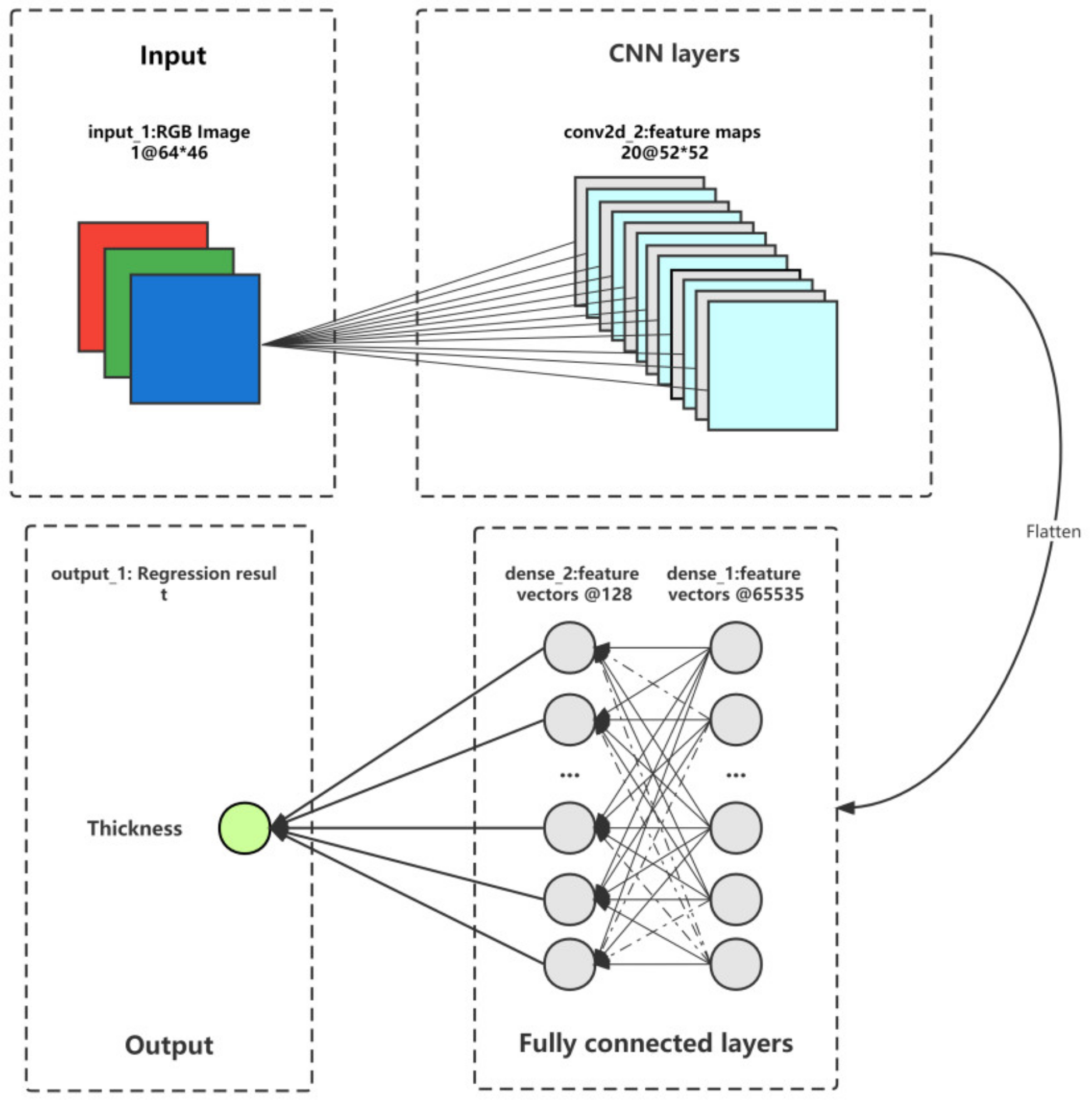
2.2.2. Overall Architecture of the Model

The model in focus is a convolutional neural network (CNN), as shown in Figure 6, a type of deep learning model that is particularly effective at processing grid-like data such as images [36,37,38,39,40]. CNNs have the ability to learn spatial hierarchies of features, making them a suitable choice for our task. Our CNN architecture consists of a convolutional layer, an activation layer, a pooling layer, and a fully connected layer. The convolutional layer is used to extract features from the image, and we chose a 3 × 3 convolutional kernel because it can extract enough features while maintaining computational efficiency. For the activation function, we chose ReLU because it can effectively solve the gradient vanishing problem and accelerate the training of the model.

2.2.3. Components of the Model

Convolutional Layer: Our deep learning model, ConvNet, begins with a convolutional layer [41,42]. This layer uses a set of 64 filters, each with a kernel size of 3 × 3, stride of 1, and padding of 1. These filters are designed to capture local patterns within the microscopic images of the solar cells, which can range from simple features such as edges and textures to more complex shapes related to the structure of the indium tin oxide (ITO) layers. The output of this layer is a set of 64 feature maps, each the same size as the input due to the padding.
O i , j = m = 0 M 1 n = 0 N 1 I i + m , j + n K m , n + b
Max Pooling Layer: Following the convolutional layer, we have a max pooling layer with a 2 × 2 window [43,44,45]. This layer is tasked with down-sampling the feature maps from the previous layer. It accomplishes this by selecting the maximum value within each 2 × 2 window, thereby preserving the most pertinent information while concurrently reducing the dimensionality of the input. This not only mitigates computational costs but also imparts a degree of translational invariance to the model, bolstering its robustness and ability to generalize from the learned features.
O i , j = max m = 0 M 1 max n = 0 N 1 I 2 i + m , 2 j + n
where K (m, n) is an element of a convolution kernel (also known as a filter or window), m and n are the coordinates of the element, and b is a bias term which is a constant that can be added to the result after the convolution operation.
Fully Connected Layers: The ConvNet model includes four fully connected layers [46,47,48]. The first fully connected layer takes the flattened output from the max pooling layer and transforms it into a 512-dimensional vector. The second and third fully connected layers further process this high-level representation, reducing the dimensionality to 256 and then to 128. Each of these layers uses a ReLU activation function to introduce non-linearity into the model, enhancing its ability to learn complex patterns. The fourth and final layer is the output layer, which transforms the 128-dimensional vector into a single value, representing the predicted thickness of the ITO layer in the solar cell. This layer does not use an activation function, as we are performing regression and want to allow for a full range of output values.
Our ConvNet model thus presents a streamlined, deep learning-driven approach for estimating the thickness of the transparent conductive oxide layers in solar cells, leveraging the power of convolutional and fully connected layers to learn from microscopic images without interrupting the production process.
Our research introduces a novel, deep learning-driven approach for estimating the thickness of the transparent conductive oxide layers in solar cells. This image-based technique, which employs deep learning algorithms, enables real-time estimation without interfering with the production process, thus enhancing manufacturing efficiency and maintaining the quality of the conductive layer. The integration of computer vision technologies has greatly benefited the field of material science, offering a more precise and efficient analysis of material surfaces.

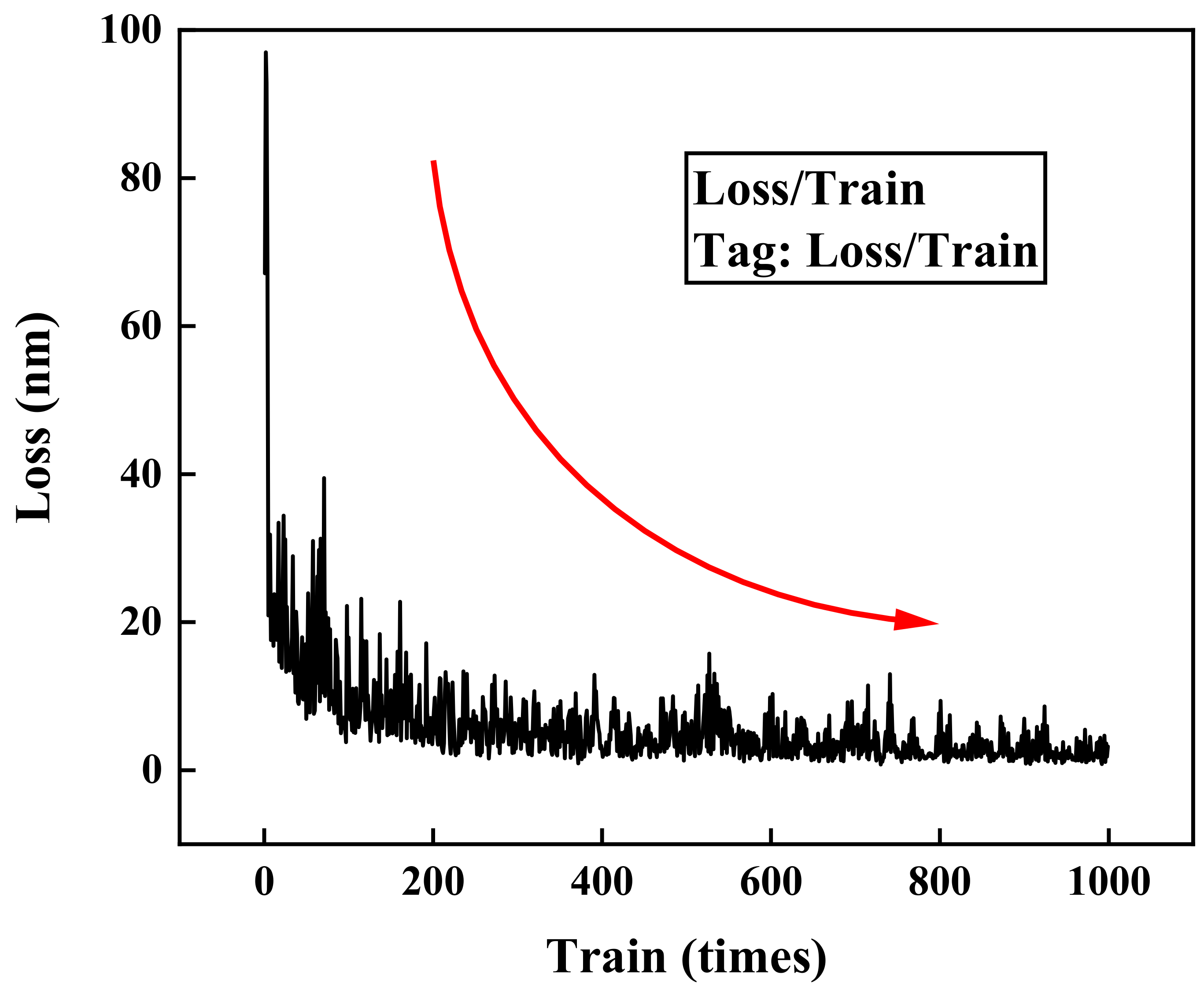
2.2.4. Training Configuration

From a mathematical standpoint, the procedure for training a machine learning model encompasses several fundamental principles:
Loss Function: The metric that quantifies the efficacy of a model by computing the discrepancy between the predicted and true values. In this context, the model employs the L1 loss, otherwise known as the mean absolute error (MAE), which calculates the average of the absolute variances between the forecasted and actual values. A compound loss function, a weighted sum of the mean squared error (MSE) and the L1 loss, is also defined [49,50]. Nonetheless, for the purpose of backpropagation and subsequent model parameter updates during the training phase, only the L1 loss is utilized.
L MAE = 1 N i = 1 N y i y i ^
L MSE = 1 N i = 1 N y i y i ^ 2
Optimizer: The mechanism used for updating the model parameters based on the gradients calculated from the loss function. In this specific case, the Adam optimizer, a popularly utilized adaptive learning rate optimization algorithm in the domain of deep learning, is employed with an initial learning rate set at 0.001.
Learning Rate and Learning Rate Scheduler: The learning rate dictates the size of each step during iterations towards the loss function’s minimum. This study incorporates a learning rate scheduler that adjusts the learning rate after every 10 epochs by a factor of 0.95, optimizing the output.
α t = α t 1 × decay _ factor
Viewing the training process from the lens of mathematical optimization, it can be seen as a problem within a multi-dimensional space, where each dimension corresponds to a parameter in the model. The objective then is to discover a set of parameters that minimizes the value of the loss function.
For every epoch, of which there are a total of 1000, the parameters of the model are updated contingent on the gradients of the loss concerning the parameters. TensorBoard, a tool that provides visual representations of the training process and aids easy debugging by displaying the model’s computational graph, is used to monitor the whole training process.
The optimal loss attained during training is continuously tracked, with the model parameters corresponding to this best loss being retained. This technique is standard practice in the field of machine learning to ensure the preservation of the model with superior performance, even if subsequent epochs do not yield improvements in performance.
We trained 1000 epochs, and the learning rate decreased from 0.01, decreasing by 10% every certain epoch, instead of a fixed 0.001. This is because using a higher learning rate in the early stage of training can help to quickly cause convergence, while in the later stage of training, decreasing the learning rate can help to avoid overfitting and improve the generalization performance of the model. Also, we chose the Adam optimization algorithm in some of our experiments because it can adaptively adjust the learning rate to improve training efficiency.

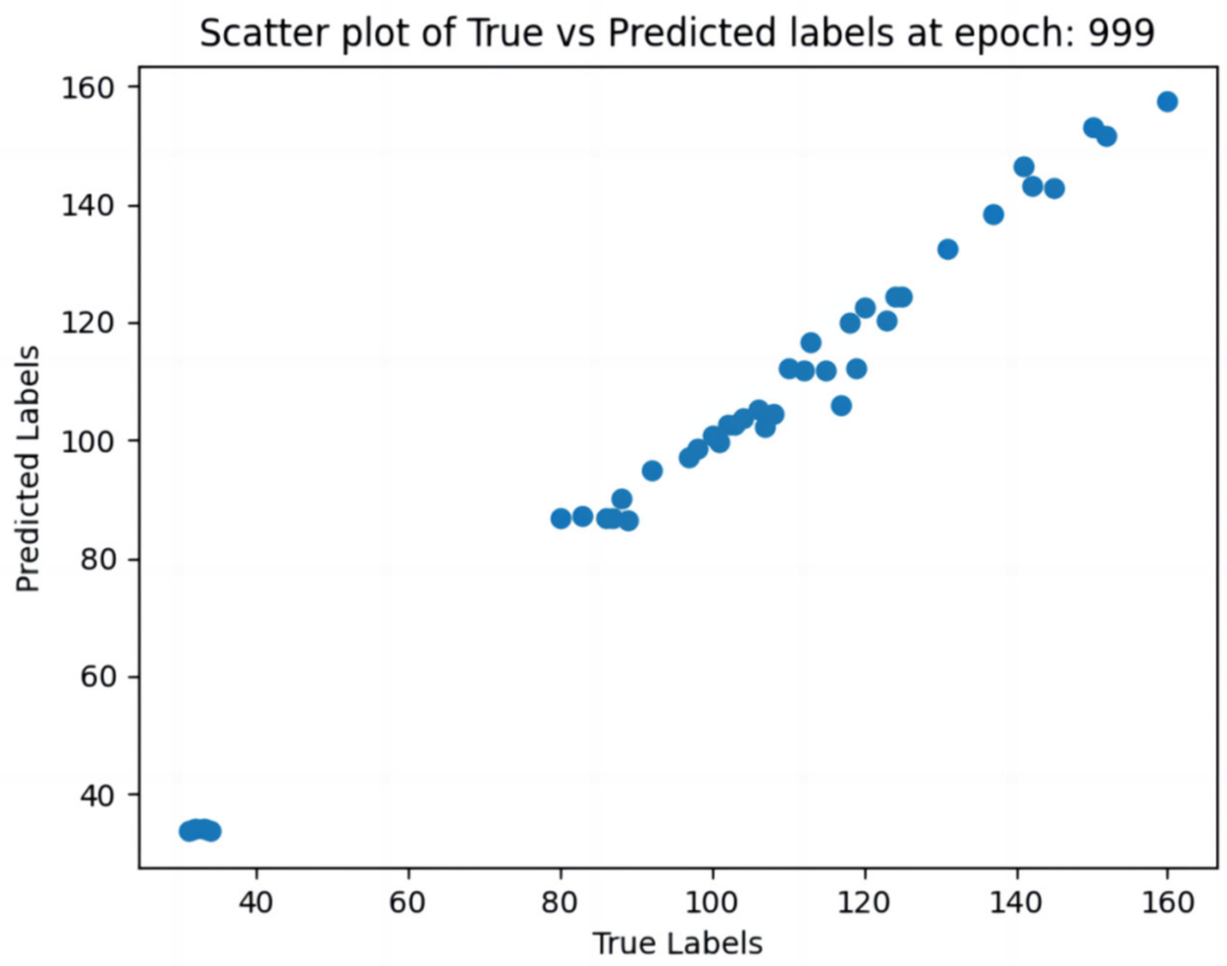
3. Results and Discussion

We ran a number of trials and evaluated the data to determine how well our suggested deep learning model performed at estimating the thickness of the ITO layers in solar cells. The performance metrics used for evaluation were the MAE and MSE. These metrics quantify the accuracy of the predictions made by the model. As shown in Figure 7, we trained our deep learning model, which combines both MAE and MSE metrics, using the training set and optimized the model parameters through the backpropagation algorithm and the Adam optimizer. The learning rate was set to 0.001, and a learning rate scheduler was employed to adjust the learning rate every 10 epochs. The model was trained for a total of 1000 epochs. Figure 7 shows the change in the value of the loss function of the model during the training process. The loss function’s value is shown by the vertical axis, while the number of training rounds or steps is represented by the horizontal axis. As can be seen, the loss value of the model decreases as the training progresses, indicating that the model is learning and gradually optimizing.
After training the model, we evaluated its performance on the validation set. The evaluation metrics MAE and MSE were calculated to assess the accuracy of the model’s predictions. The MAE and MSE achieved by our model were found to be 0.83 nm. This indicates that, on average, the model’s predictions deviated from the ground truth values by approximately 0.83 nm. A lower MAE value suggests higher accuracy in estimating the TCO layer thickness. This indicates the average magnitude of the errors made by the model in predicting the ITO layer thickness. A lower MSE value indicates better overall performance.
Figure 8 shows the comparison between the predicted and true values of the model in the form of a scatter plot. The horizontal axis denotes the true value, while the vertical axis signifies the predicted value. Ideally, all points should be on a line with a slope of 1 and an intercept of 0. This means that the model’s predicted results are exactly the same as the true values.
We observe that the majority of prediction errors are centered around zero, indicating that the model’s predictions are generally close to the true values. However, there is a small portion of predictions with larger errors, indicating some degree of variability and potential room for improvement.
Upon closer examination of these larger errors, we identified several potential sources of inaccuracies. These include variations in the lighting conditions during data collection, noise in the images, and limitations in the optical interference phenomenon model used. Addressing these factors could potentially lead to improved accuracy in future iterations of the model.
Overall, our deep learning model demonstrates promising performance in estimating the thickness of the transparent conductive oxide layers in solar cells. The achieved MAE and MSE indicate the model’s ability to make reasonably accurate predictions.

4. Conclusions

In this paper, we presented a novel deep learning-driven approach for estimating the thickness of the transparent conductive oxide (ITO) layers in solar cells. Our image-based technique leverages the power of convolutional neural networks (CNNs) to analyze microscopic images of solar cells and predict the thickness of the conductive layer.
Our method can be used to inspect the quality of a cell, for example, to detect defects or the uneven thickness of a layer, during solar cell manufacturing. In other related industries, such as semiconductor manufacturing, our methods can be used to inspect the quality of wafers, such as by detecting cracks or impurities.
The experimental results demonstrate that our deep learning model can accurately estimate the thickness of the ITO layers in solar cells. We chose a combination of MAE and MSE because MAE is insensitive to outliers, while MSE has a greater penalty for large errors. This combination minimizes the prediction error while ensuring model robustness. The low MAE and MSE values indicate the effectiveness of our approach. Compared to traditional measurement methods, our image-based approach offers real-time estimation without interrupting the production process, enhancing manufacturing efficiency.
The integration of computer vision technologies, such as deep learning and CNNs, has significant potential in various domains, including material science. By combining computer vision with machine learning techniques, researchers can process and analyze images more efficiently and make critical predictions and decisions.
Future work could focus on further improving the performance of the deep learning model by exploring different network architectures or incorporating additional data augmentation techniques. Additionally, the application of our approach to other thin film measurements or material characterization tasks could be investigated to extend its potential impact. Our method relies heavily on the phenomenon of light interference, so if the surface of the ITO layer is not flat, or the intensity of the light source is not stable, it may affect the accuracy of the results. We will explore how to solve these problems in future research.
Overall, our research contributes to the field of environmentally friendly energy conversion by providing a real-time, non-contact approach for determining the thickness of the transparent conductive oxide layers in solar cells, which has both practical and scientific importance. Furthermore, because our deep learning model offers the advantage of non-contact measurement, it eliminates the need for physical contact with solar cells. This non-intrusive approach reduces the risk of damage to the cells and ensures the integrity of the conductive layer.

Author Contributions

Conceptualization, methodology, software, investigation, and writing—original draft preparation, X.F. and B.W.; formal analysis and investigation, M.Q.K. and M.A.Z.; resources, data curation, writing—review and editing, validation, and visualization, D.P.P.; supervision, project administration, funding acquisition, and validation, J.Y. All authors have read and agreed to the published version of the manuscript.

Funding

This research was supported and granted by the New and Renewable Energy Technology Development Program of the Korea Institute of Energy Technology Evaluation and Planning (KETEP) funded by the Korean Ministry of Trade, Industry and Energy (MOTIE) (Project No. 20213030010240 and 20213030010400).

Data Availability Statement

Not applicable.

Conflicts of Interest

The authors declare no conflict of interest.

References

  1. Grätzel, M. Solar energy conversion by dye-sensitized photovoltaic cells. Inorg. Chem. 2005, 44, 6841–6851. [Google Scholar] [CrossRef]
  2. Bagher, A.M.; Vahid, M.M.A.; Mohsen, M. Types of solar cells and application. Am. J. Opt. Photonics 2015, 3, 94–113. [Google Scholar] [CrossRef]
  3. Hayat, M.B.; Ali, D.; Monyake, K.C.; Alagha, L.; Ahmed, N. Solar energy—A look into power generation, challenges, and a solar-powered future. Int. J. Energy Res. 2019, 43, 1049–1067. [Google Scholar] [CrossRef]
  4. Sulaman, M.; Yang, S.Y.; Zhang, Z.H.; Imran, A.; Bukhtiar, A.; Ge, Z.H.; Tang, Y.; Jiang, Y.R.; Tang, L.B.; Zou, B.S. Lead-free tin-based perovskite nanocrystals for high-performance self-driven bulk-heterojunction photodetectors. Mater. Today Phys. 2022, 27, 1100829. [Google Scholar] [CrossRef]
  5. Hu, Z.; Wang, J.; Ma, X.; Gao, J.; Xu, C.; Yang, K.; Wang, Z.; Zhang, J.; Zhang, F. A critical review on semitransparent organic solar cells. Nano Energy 2020, 78, 105376. [Google Scholar] [CrossRef]
  6. Roy, P.; Sinha, N.K.; Tiwari, S.; Khare, A. A review on perovskite solar cells: Evolution of architecture, fabrication techniques, commercialization issues and status. Sol. Energy 2020, 198, 665–688. [Google Scholar] [CrossRef]
  7. Riede, M.; Spoltore, D.; Leo, K. Organic solar cells—the path to commercial success. Adv. Energy Mater. 2021, 11, 2002653. [Google Scholar] [CrossRef]
  8. Massiot, I.; Cattoni, A.; Collin, S. Progress and prospects for ultrathin solar cells. Nat. Energy 2020, 5, 959–972. [Google Scholar] [CrossRef]
  9. Andreani, L.C.; Bozzola, A.; Kowalczewski, P.; Liscidini, M.; Redorici, L. Silicon solar cells: Toward the efficiency limits. Adv. Phys. X 2019, 4, 1548305. [Google Scholar] [CrossRef]
  10. Le, A.H.T.; Dao, V.A.; Pham, D.P.; Kim, S.; Dutta, S.; Nguyen, C.P.T.; Lee, Y.; Kim, Y.; Yi, J. Damage to passivation contact in silicon heterojunction solar cells by ITO sputtering under various plasma excitation modes. Sol. Energy Mater. Sol. Cells 2019, 192, 36–43. [Google Scholar] [CrossRef]
  11. Sousa, M.G.; Da Cunha, A.F. Optimization of low temperature RF-magnetron sputtering of indium tin oxide films for solar cell applications. Appl. Surf. Sci. 2019, 484, 257–264. [Google Scholar] [CrossRef]
  12. Amalathas, A.P.; Alkaisi, M.M. Effects of film thickness and sputtering power on properties of ITO thin films deposited by RF magnetron sputtering without oxygen. J. Mater. Sci. Mater. Electron. 2016, 27, 11064–11071. [Google Scholar] [CrossRef]
  13. Pla, J.; Tamasi, M.; Rizzoli, R.; Losurdo, M.; Centurioni, E.; Summonte, C.; Rubinelli, F. Optimization of ITO layers for applications in a-Si/c-Si heterojunction solar cells. Thin Solid Film. 2003, 425, 185–192. [Google Scholar] [CrossRef]
  14. Huang, M.; Hameiri, Z.; Aberle, A.G.; Mueller, T. Comparative study of amorphous indium tin oxide prepared by pulsed-DC and unbalanced RF magnetron sputtering at low power and low temperature conditions for heterojunction silicon wafer solar cell applications. Vacuum 2015, 119, 68–76. [Google Scholar] [CrossRef]
  15. Hotovy, J.; Hüpkes, J.; Böttler, W.; Marins, E.; Spiess, L.; Kups, T.; Smirnov, V.; Hotovy, I.; Kováč, J. Sputtered ITO for application in thin-film silicon solar cells: Relationship between structural and electrical properties. Appl. Surf. Sci. 2013, 269, 81–87. [Google Scholar] [CrossRef]
  16. Dao, V.A.; Choi, H.; Heo, J.; Park, H.; Yoon, K.; Lee, Y.; Kim, Y.; Lakshminarayan, N.; Yi, J. rf-Magnetron sputtered ITO thin films for improved heterojunction solar cell applications. Curr. Appl. Phys. 2010, 10, S506–S509. [Google Scholar] [CrossRef]
  17. Muneshwar, T.P.; Varma, V.; Meshram, N.; Soni, S.; Dusane, R.O. Development of low temperature RF magnetron sputtered ITO films on flexible substrate. Sol. Energy Mater. Sol. Cells 2010, 94, 1448–1450. [Google Scholar] [CrossRef]
  18. Alzaid, M.; Mohamed, W.S.; El-Hagary, M.; Shaaban, E.R.; Hadia, N.M.A. Optical properties upon ZnS film thickness in ZnS/ITO/glass multilayer films by ellipsometric and spectrophotometric investigations for solar cell and optoelectronic applications. Opt. Mater. 2021, 118, 111228. [Google Scholar] [CrossRef]
  19. Emam-Ismail, M.; El-Hagary, M.; El-Sherif, H.M.; El-Naggar, A.M.; El-Nahass, M.M. Spectroscopic ellipsometry and morphological studies of nanocrystalline NiO and NiO/ITO thin films deposited by e-beams technique. Opt. Mater. 2021, 112, 110763. [Google Scholar] [CrossRef]
  20. Baldner, F.O.; Costa, P.B.; Gomes, J.F.S.; Leta, F.R. A review on computer vision applied to mechanical tests in search for better accuracy. In Advances in Visualization and Optimization Techniques for Multidisciplinary Research: Trends in Modelling and Simulations for Engineering Applications; Springer: Berlin/Heidelberg, Germany, 2020; pp. 265–281. [Google Scholar]
  21. Rong, D.; Xie, L.; Ying, Y. Computer vision detection of foreign objects in walnuts using deep learning. Comput. Electron. Agric. 2019, 162, 1001–1010. [Google Scholar] [CrossRef]
  22. DeCost, B.L.; Holm, E.A. A computer vision approach for automated analysis and classification of microstructural image data. Comput. Mater. Sci. 2015, 110, 126–133. [Google Scholar] [CrossRef]
  23. Holm, E.A.; Cohn, R.; Gao, N.; Matson, T.P.; Lei, B.; Yarasi, S.R. Overview: Computer vision and machine learning for microstructural characterization and analysis. Metall. Mater. Trans. A 2020, 51, 5985–5999. [Google Scholar] [CrossRef]
  24. Sethian, J.A. Level Set Methods and Fast Marching Methods: Evolving Interfaces in Computational Geometry, Fluid Mechanics, Computer Vision, and Materials Science; Cambridge University Press: Cambridge, UK, 1999. [Google Scholar]
  25. DeCost, B.L.; Holm, E.A. Characterizing powder materials using keypoint-based computer vision methods. Comput. Mater. Sci. 2017, 126, 438–445. [Google Scholar] [CrossRef]
  26. Wang, S.Y.; Zhang, P.Z.; Zhou, S.Y.; Wei, D.B.; Ding, F.; Li, F.K. A computer vision based machine learning approach for fatigue crack initiation sites recognition. Comput. Mater. Sci. 2020, 171, 109259. [Google Scholar] [CrossRef]
  27. Cifuentes-Alcobendas, G.; Domínguez-Rodrigo, M. More than meets the eye: Use of computer vision algorithms to identify stone tool material through the analysis of cut mark micro-morphology. Archaeol. Anthropol. Sci. 2021, 13, 167. [Google Scholar] [CrossRef]
  28. Karthikeyan, S.; Subbarayan, M.R.; Beemaraj, R.K.; Sivakandhan, C. Computer vision-based surface roughness measurement using artificial neural network. Mater. Today Proc. 2022, 60, 1325–1328. [Google Scholar]
  29. Yang, Y.; Qiu, T.; Kong, F.; Fan, J.; Ou, H.; Xu, Q.; Chu, P.K. Interference effects on indium tin oxide enhanced Raman scattering. J. Appl. Phys. 2012, 111, 33110. [Google Scholar] [CrossRef]
  30. Granlund, T.; Pettersson, L.A.A.; Anderson, M.R.; Inganäs, O. Interference phenomenon determines the color in an organic light emitting diode. J. Appl. Phys. 1997, 81, 8097–8104. [Google Scholar] [CrossRef]
  31. Halliday, D.; Resnick, R.; Walker, J. Fundamentals of Physics; John Wiley & Sons: Hoboken, NJ, USA, 2013. [Google Scholar]
  32. Ni, Z.; Mou, S.; Zhou, T.; Cheng, Z. Broader color gamut of color-modulating optical coating display based on indium tin oxide and phase change materials. Appl. Opt. 2018, 57, 3385–3389. [Google Scholar] [CrossRef]
  33. Lyu, Y.; Mou, S.; Ni, Z.; Bai, Y.; Sun, Y.; Cheng, Z. Multi-color modulation of solid-state display based on thermally induced color changes of indium tin oxide and phase changing materials. Opt. Express 2017, 25, 1405–1412. [Google Scholar] [CrossRef]
  34. Born, M.; Wolf, E. Principles of Optics: Electromagnetic Theory of Propagation, Interference and Diffraction of Light; Elsevier: Amsterdam, The Netherlands, 2013. [Google Scholar]
  35. Hariharan, P. Optical Interferometry, 2nd ed.; Elsevier: Amsterdam, The Netherlands, 2003. [Google Scholar]
  36. Tan, M.; Le, Q. Efficientnet: Rethinking model scaling for convolutional neural networks. In Proceedings of the International Conference on Machine Learning, PMLR, Long Beach, CA, USA, 9–15 June 2019; pp. 6105–6114. [Google Scholar]
  37. Yamashita, R.; Nishio, M.; Do, R.G.; Togashi, K. Convolutional neural networks: An overview and application in radiology. Insights Imaging 2018, 9, 611–629. [Google Scholar] [CrossRef] [PubMed]
  38. Albawi, S.; Mohammed, T.A.; Al-Zawi, S. Understanding of a convolutional neural network. In Proceedings of the 2017 International Conference on Engineering and Technology (ICET), IEEE, Antalya, Turkey, 21–23 August 2017; pp. 1–6. [Google Scholar]
  39. O’Shea, K.; Nash, R. An introduction to convolutional neural networks. arXiv 2015, arXiv:1511.08458. [Google Scholar]
  40. Gu, J.; Wang, Z.; Kuen, J.; Ma, L.; Shahroudy, A.; Shuai, B.; Liu, T.; Wang, X.; Wang, G.; Cai, J.; et al. Recent advances in convolutional neural networks. Pattern Recognit. 2018, 77, 354–377. [Google Scholar] [CrossRef]
  41. Bayar, B.; Stamm, M.C. A deep learning approach to universal image manipulation detection using a new convolutional layer. In Proceedings of the 4th ACM Workshop on Information Hiding and Multimedia Security, Vigo, Spain, 20–22 June 2016; pp. 5–10. [Google Scholar]
  42. Cordonnier, J.B.; Loukas, A.; Jaggi, M. On the relationship between self-attention and convolutional layers. arXiv 2019, arXiv:1911.03584. [Google Scholar]
  43. Giusti, A.; Cireşan, D.C.; Masci, J.; Gambardella, L.M.; Schmidhuber, J. Fast image scanning with deep max-pooling convolutional neural networks. In Proceedings of the 2013 IEEE International Conference on Image Processing, IEEE, Melbourne, VIC, Australia, 15–18 September 2013; pp. 4034–4038. [Google Scholar]
  44. Graham, B. Fractional max-pooling. arXiv 2014, arXiv:1412.6071. [Google Scholar]
  45. Nagi, J.; Ducatelle, F.; Di Caro, G.A.; Cireşan, D.; Meier, U.; Giusti, A.; Nagi, F.; Schmidhuber, J.; Gambardella, L.M. Max-pooling convolutional neural networks for vision-based hand gesture recognition. In Proceedings of the 2011 IEEE International Conference on Signal and Image Processing Applications (ICSIPA), Kuala Lumpur, Malaysia, 16–18 November 2011; pp. 342–347. [Google Scholar]
  46. Basha SH, S.; Dubey, S.R.; Pulabaigari, V.; Mukherjee, S. Impact of fully connected layers on performance of convolutional neural networks for image classification. Neurocomputing 2020, 378, 112–119. [Google Scholar] [CrossRef]
  47. Ding, X.; Xia, C.; Zhang, X.; Chu, X.; Han, J.; Ding, G. Repmlp: Re-parameterizing convolutions into fully-connected layers for image recognition. arXiv 2021, arXiv:2105.01883. [Google Scholar]
  48. Zhang, C.L.; Luo, J.H.; Wei, X.S.; Wu, J. In defense of fully connected layers in visual representation transfer. In Advances in Multimedia Information Processing, Proceedings of the PCM 2017: 18th Pacific-Rim Conference on Multimedia, Harbin, China, 28–29 September 2017; Revised Selected Papers, Part II 18; Springer International Publishing: Berlin/Heidelberg, Germany, 2018; pp. 807–817. [Google Scholar]
  49. Chai, T.; Draxler, R.R. Root mean square error (RMSE) or mean absolute error (MAE)–Arguments against avoiding RMSE in the literature. Geosci. Model Dev. 2014, 7, 1247–1250. [Google Scholar] [CrossRef]
  50. Willmott, C.J.; Matsuura, K. Advantages of the mean absolute error (MAE) over the root mean square error (RMSE) in assessing average model performance. Clim. Res. 2005, 30, 79–82. [Google Scholar] [CrossRef]
Figure 1. Experimental flow chart.
Energies 16 06049 g001
Figure 2. (a) Isotropic interference diagram. (b) Equal thickness interference diagram.
Energies 16 06049 g002
Figure 3. (a) Theoretical calculation of color distribution. (b) Actual measurement of color distribution (x-axis: number of pixels; y-axis: bins).
Energies 16 06049 g003aEnergies 16 06049 g003b
Figure 4. ITO samples of different thicknesses measured by an ellipsometer.
Energies 16 06049 g004
Figure 5. (a) Data collection device and (b) a portion of the collected data images.
Energies 16 06049 g005
Figure 6. Proposed network structure that can be regressed from images to plating thickness values.
Energies 16 06049 g006
Figure 7. Model training loss function change graph.
Energies 16 06049 g007
Figure 8. Scatter plot of prediction error.
Energies 16 06049 g008
Disclaimer/Publisher’s Note: The statements, opinions and data contained in all publications are solely those of the individual author(s) and contributor(s) and not of MDPI and/or the editor(s). MDPI and/or the editor(s) disclaim responsibility for any injury to people or property resulting from any ideas, methods, instructions or products referred to in the content.

