1. Introduction
Nowadays, power converter technologies play a significant role in various applications, such as electric transportation [
1], electric aircraft [
2,
3], and energy conversion systems [
4,
5], due to their efficient management of electrical energy. The increasing adoption of power electronic converters in energy systems can be attributed to the growing use of renewable energies such as solar and wind power [
6]. In renewable energy applications, addressing power quality has become a primary concern for all grid-connected power converters to comply with grid codes [
7,
8]. In this sense, power quality issues involve deviations from the ideal sinusoidal waveform in magnitude and frequency, impacting both grid- and load-side currents and voltages [
9,
10]. Recent research has proposed various approaches to enhance the efficiency of voltage source converters (VSC) and mitigate power-quality-related losses [
11,
12,
13]. The rapid progress in power converters has been furthered by the development of high-performance microprocessors capable of implementing advanced nonlinear digital controllers. Moreover, the field of power electronic semiconductors has made significant strides in creating new high-speed switching devices with remarkably low on-state losses. Among the promising power electronic semiconductors, SiC-MOSFET is particularly interesting in power applications, due to its dynamic behavior in terms of high switching frequencies, which is why it is employed in this study. Consequently, these advancements enable the design of more compact power electronic converters compared to traditional ones [
14].
From the point of view of the conventional AC-DC-AC, the two-level voltage source converters (2L-VSCs) are still some of the most used converters for many applications, and, nowadays, the 2L-VSCs are considered the fundamental components in both industrial applications and renewable energies. However, the limited number of output voltage levels creates challenges related to losses and power quality, attributed to their unfavorable harmonic profiles [
15,
16]. In this sense, the modular multilevel converter (MMC) has garnered attention from the industry and energy sectors, due to its ability to solve the problems associated with harmonic distortion. This converter demonstrates the ability to generate sinusoidal voltages and currents with minimal harmonic distortions. Among the MMC topologies, the cascade H-Bridge (CHB) configuration stands out as a popular choice due to its inherent modularity, facilitating scalability to generate higher MMC voltage levels. Additionally, the CHB-based MMC design avoids the need to incorporate an extensive array of flying capacitors or clamping diodes in the power converter topology [
17]. Consequently, one of the most widely discussed topologies in the literature is the seven-level voltage source converter (7L-VSC) based on three CHB cells in series per phase [
18]. However, both 2L-VSC and 7L-VSC topologies are based on AC-DC-AC configurations, which require the inclusion of an intermediate stage of energy storage elements such as capacitor banks. These additional components contribute to increased weight and volume, and, above all, these capacitors add the possibility of failure in the VSCs. In this sense, recent research efforts have focused on the development of a versatile direct AC-AC power interface that adopts a modular architecture. This innovative approach enables the interconnection of AC sources to the grid and load side without the need for energy storage elements. Within this context, the matrix converter (MC) has emerged as a promising solution. The MC facilitates the generation of a three-phase sinusoidal voltage with an adjustable amplitude and frequency by utilizing fully controlled bi-directional switches, eliminating the requirement for energy storage elements [
19].
Among these VSC topologies, the most commonly employed power semiconductor devices are IGBTs. However, SiC-MOSFETs have gained attention as an alternative due to their ability to operate at higher switching frequencies compared to IGBTs [
20,
21,
22]. Nevertheless, simply incorporating faster switching devices is insufficient to improve power quality. It is crucial to prioritize the design of the entire converter to ensure enhanced performance at high switching frequencies with power semiconductor devices [
23,
24]. This article presents a comprehensive approach to the design of voltage source converters, focusing particularly on three types of converters based on SiC-MOSFET semiconductor devices. This article is divided as follows.
Section 2 introduces the H-Bridge cell design. Then, in
Section 3, the 2L-VSC based on CHB cells in a paralell configuration is presented, and the experimental results under fault conditions are analyzed. In
Section 4, the 7L-VSC topology is addressed. In
Section 5, the MC design and experimental results are presented. Finally, the main conclusions of this work are given in the last section.
2. H-Bridge Cell-Based Converters
In recent years, the trend in power electronics design has shifted towards modular solutions. Modularity enables the scalability of the converter, allowing for an increase in power capacity by arranging several H-Bridge cells in parallel. Alternatively, assembling cells in series can result in a multilevel converter. A modular design for an H-Bridge cell must consider various aspects, such as the switching signals of the power semiconductors, the generation of dead times, and the implementation of protection circuits. These considerations are essential to provide robustness to the H-Bridge cell and ensure its reliable operation. Furthermore, the use of a modular approach can also simplify maintenance and repair processes, as individual cells can be replaced if necessary, without affecting the entire system. Overall, the modular design approach offers several advantages, including scalability, robustness, and ease of maintenance, making it a popular choice for power converter design [
25]. The subsequent sections cover the electronic circuits of each module comprising an H-Bridge cell. An exhaustive description of the H-Bridge cell design can be found in [
13].
2.1. Switching Signal Drivers
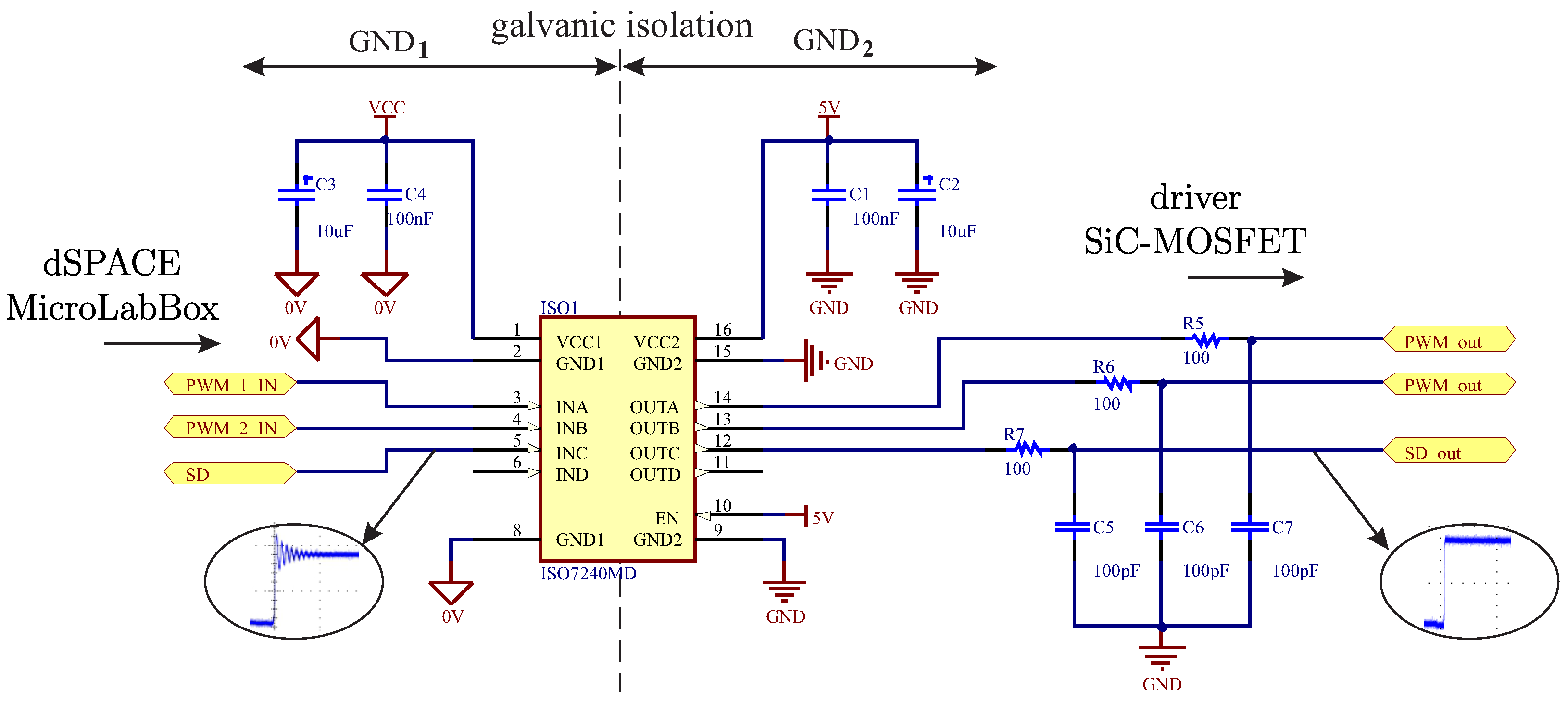
The switching signal drivers are essential components in the control circuits of SiC-MOSFET semiconductor devices; they ensure the proper operation of the power conversion system. However, these drivers are susceptible to the electrical noise generated by the high-frequency switching of the power semiconductor device. To overcome this issue, it is necessary to incorporate a galvanic isolation stage in the driver circuit. This galvanic isolation stage helps in achieving immunity to electrical noise and ensures the stable operation of the power conversion system. The driver circuit, as shown in
Figure 1, exhibits an under-damped characteristic of the input signal from the control module to the galvanic isolator. To compensate for this under-damping, a passive low-pass filter is used. The design of this filter takes into consideration the maximum switching frequency of the power semiconductor device, and it helps in reducing the noise and improving the performance of the driver circuit.
2.2. Dead Time Generation Circuit
In addition to galvanic isolation, it is also crucial to implement dead time in the complementary signals applied to the half-H-Bridge. Dead time is a brief interval where both switches in the half-H-Bridge are turned off to avoid short circuits between edge changes in the switching signals [
26]. This ensures that the output voltage is always proportional to the control signal and reduces the likelihood of power device failure due to short circuits.
Figure 2 displays the driver circuitry, where the application of dead time is evident in the complementary signals [
27]. The input signal from the control module to the galvanic isolator exhibits an under-damped characteristic, which is compensated for by the use of a passive low-pass filter. The filter is designed to suppress high-frequency noise generated by the switching of the power semiconductor device, while considering the maximum switching frequency.
2.3. Gate Complementary Signal Generation
The IR2110S device, as a high-voltage, high-speed power MOSFET and IGBT driver with independent high- and low-side referenced output channels, is crucial in properly driving the high-side devices of a bridge circuit, as well as the low-side devices. As shown in
Figure 3, the gate driver circuit employs a bootstrap circuit, which provides the required voltage to the high-side devices. Specifically, the bootstrap capacitor C1 is charged by the voltage across the low-side device and then used to switch the high-side device [
28]. The advantage of this configuration is that it allows for the use of a single isolated power supply for the driver circuit, thereby reducing the overall system complexity and cost. Moreover, the IR2110S device incorporates an under-voltage lockout function, which ensures that the power MOSFETs and IGBTs are not damaged due to insufficient voltage levels, thus improving the reliability of the circuit.
2.4. Power Board for the H-Bridge
The multilevel converter design approach seeks to combine cells in an H-Bridge arrangement, connecting them in series to achieve higher output voltage levels. This configuration allows us to achieve a scalable and modular design. The device selected to mount the power board for the H-Bridge cell design is CREE Semiconductor’s CAS120M12BM2, which is a power component that features two SiC-MOSFET transistors connected in a half-H-Bridge configuration. This device is characterized by low conduction resistance and a significantly higher switching speed than conventional switching devices such as IGBTs.
Table 1 shows the most relevant parameters of the selected SiC-MOSFET [
29].
Figure 4 shows the scheme proposed for the design of the power board for the complete H-Bridge scheme.
2.5. H-Bridge Cell Experimental Test
The values of the technical parameters for the experimental tests of the H-Bridge cell are shown in
Table 2. In the oscillogram of
Figure 5a, the output signals
and
from the signal conditioner can be observed. As can be seen, the
and
signals do not present overshoots or oscillations, mainly due to the action of the low-pass RC filter, although they do present a slight attenuation in amplitude due to the signal passing through the filter. However, this last characteristic does not affect the general operation of the triggering system. Subsequently, the
and
signals obtained from the conditioning circuit pass to the block responsible for generating the complements of each branch of the H-Bridge cell, to then generate the dead time. This generation of dead time can be observed in the oscillogram of
Figure 5b, where an enlargement of the signal graph can also be appreciated for the better identification of dead time generation. The measured value of the dead time is approximately 1
s for a switching frequency of 100 kHz. The dead time is obtained by a circuit composed of logic gates from the 74HC86 series and combined with resistive and capacitive elements.
The complementary PWM signals generated by the control circuits implemented using the IR2110S integrated circuit are sent to each SiC-MOSFET device to perform the corresponding switching. Each IR2110S integrated circuit controls one branch of a H-Bridge, so two IR2110S are required to implement a cell. In the oscillogram of
Figure 5c, the trigger signals can be observed, which have a delay time during the high and low transitions. These delays are due to the input parasitic capacitances of the SiC-MOSFET devices, which, together with the resistance
, form a low-pass filter that produces slight distortion in the control signal. On the other hand, to analyze the switching characteristics, it is necessary to measure the current signals
and voltage signals
on the power device. Desirable characteristics such as reduced overshoot or oscillations are observed. These characteristics can be seen in the oscillogram of
Figure 5d, where a simultaneous representation of the voltage (
) and current (
) signals can be observed.
The output voltage (
) and output current (
) are shown in the oscillogram of
Figure 5e. It can be observed that the signal
has a smoother transition between high and low levels compared to the output voltage (
), mainly due to the inductive nature of the load connected to the converter to perform the preliminary experimental tests. It can be seen that the output signals do not present significant overshoot or oscillations; therefore, their response is as expected for the type of load considered during the test.
3. Two-Level Multimodular VSC Topology
The scalable 2L-VSC topology consists of parallel-connected H-Bridge cells, as shown in the schematic of
Figure 6a. The modular characteristic makes it particularly useful for applications where a compact converter, high energy density, and good reliability are required. This is possible by incorporating a redundant scheme, constituting an advantage compared to conventional converters. The characteristics of a simple and compact power circuit, scalability in terms of nominal power, and the possibility of operation in the event of faults due to the redundancy of modules connected in parallel result in a more robust, economical, and flexible VSC compared to traditional configurations.
From the point of view of the power semiconductor devices, SiC-MOSFETs have a comparative advantage in terms of switching losses and switching frequencies, compared to IGBT-type semiconductor devices. The implemented scalable multimodular 2L-VSC, which is shown in
Figure 6b, integrates SiC-MOSFET-type semiconductors, and its switching hardware has been designed to achieve switching frequencies close to 100 kHz.
Two-Level Multimodular VSC Experimental Results
The parameters used in the experimental test bench of the 2L-VSC are shown in
Table 3. In
Figure 7a, the output voltage of the 2L-VSC can be observed before the output filter (
), where a switched waveform generated by the PWM modulation applied to the converter can be seen. After the output filter, a sinusoidal waveform without harmonics is observed because the output filter is configured as a low-pass filter, attenuating high-order harmonics. At the same time, the current distribution in two modules connected in parallel is illustrated in
Figure 7b, where it can be concluded that the current distribution per module is practically equivalent.
On the other hand,
Figure 7c depicts the voltages of the three phases measured at the point of common coupling (PCC) at the three-phase load side. The applied voltage to the load generates a symmetric current flow across the two parallel-connected cells (
and
), resulting in a quantified current of 3.72 A peak-to-peak on the load.
Figure 7d illustrates how the current on cell 2 (
) doubles to keep the current in the load (
) constant when cell 1 is intentionally disconnected (
= 0 A), emulating post-fault behavior. These experimental results demonstrate the robustness of the proposed 2L-VSC with redundant cells operating in parallel, making it particularly useful for those applications where high reliability is required.
4. Seven-Level Multimodular VSC Topology
The scalable 7L-VSC topology, which is based on CHB cells, consists of three independent cells per phase connected in series with an independent DC-link (
), as depicted in
Figure 8a. This operational scheme incorporates SiC-MOSFET switching semiconductor devices and an output inductance
, which operates as a filter at the output of the converter. The DC-link voltage (
) serves as the energy source, while the switching semiconductors synthesize the signals that are injected into the load at the connection point. The output inductance attenuates the harmonic effects resulting from the switching of the power devices in the converter.
Figure 8b illustrates the integration of the different elements that comprise the experimental test bench of the 7L-VSC. One notable advantage of this design is its versatility and modularity, allowing for multiple configurations with minimal changes to the converter’s structure. Additionally, it is possible to expand the number of levels by adding more cascaded cells.
Seven-Level Multimodular VSC Experimental Results
The 7L-VSC tests are performed by interconnecting three cells in cascade per phase. The multilevel VSI experimental platform is composed of cascaded interconnected H-Bridge cells, where each H-Bridge cell consists of an independent DC voltage that is applied through continuous sources and provides the necessary DC-link voltage for each H-Bridge. The values of the technical parameters for the experiments are shown in
Table 4.
Figure 9a shows the output voltage of one phase of the 7L-VSC before the output filter and the current
generated on the resistive load for phase “a”. These graphs demonstrate that the current supplied to the load exhibits low harmonic distortion, which is expected due to the multilevel converter’s capability to generate sinusoidal signals.
Figure 9b shows the output currents of the seven-level multimodular converter at the point of common coupling applied to a three-phase load.
5. Voltage Source Matrix Converter Topology
The matrix converter (MC) is a single-stage AC-AC converter capable of directly supplying an “
n” phase load from an “
m” phase source (
MC), without the need for intermediate AC-DC conversion stages [
30]. The main advantages of MCs compared to widely used back-to-back conversion systems, which consist of rectifier stages connected to an inverter with an intermediate energy storage stage (capacitor bank), are as follows: reduced size, light weight and long lifespan due to the absence of large electrolytic capacitors in the main circuit, and high efficiency due to the single power conversion stage, resulting in fewer switch losses compared to two-stage converters. Given these advantages, MCs are currently used in a wide range of AC-AC conversion applications, such as industrial applications requiring variable-speed electric motor drives, electric mobility, and, more recently, wind energy conversion systems [
31,
32]. The general topology for the MC is shown in
Figure 10a. In this case, a voltage source matrix converter (VSMC) is obtained. To achieve good performance, the VSMC should be equipped with a source filter. The source filter is generally required to minimize high-frequency components in the input currents and reduce the impact of disturbances on the input grid. However, the size of the filter elements is inversely proportional to the VSMC’s switching frequency.
Figure 10b shows the implemented experimental setup of the VSMC based on bidirectional switches designed using SiC-MOSFET semiconductor devices.
5.1. Bidirectional Switch Design
The bidirectional switch (Bi-Sw) design is divided into two main parts, the dominated control block and power block, respectively.
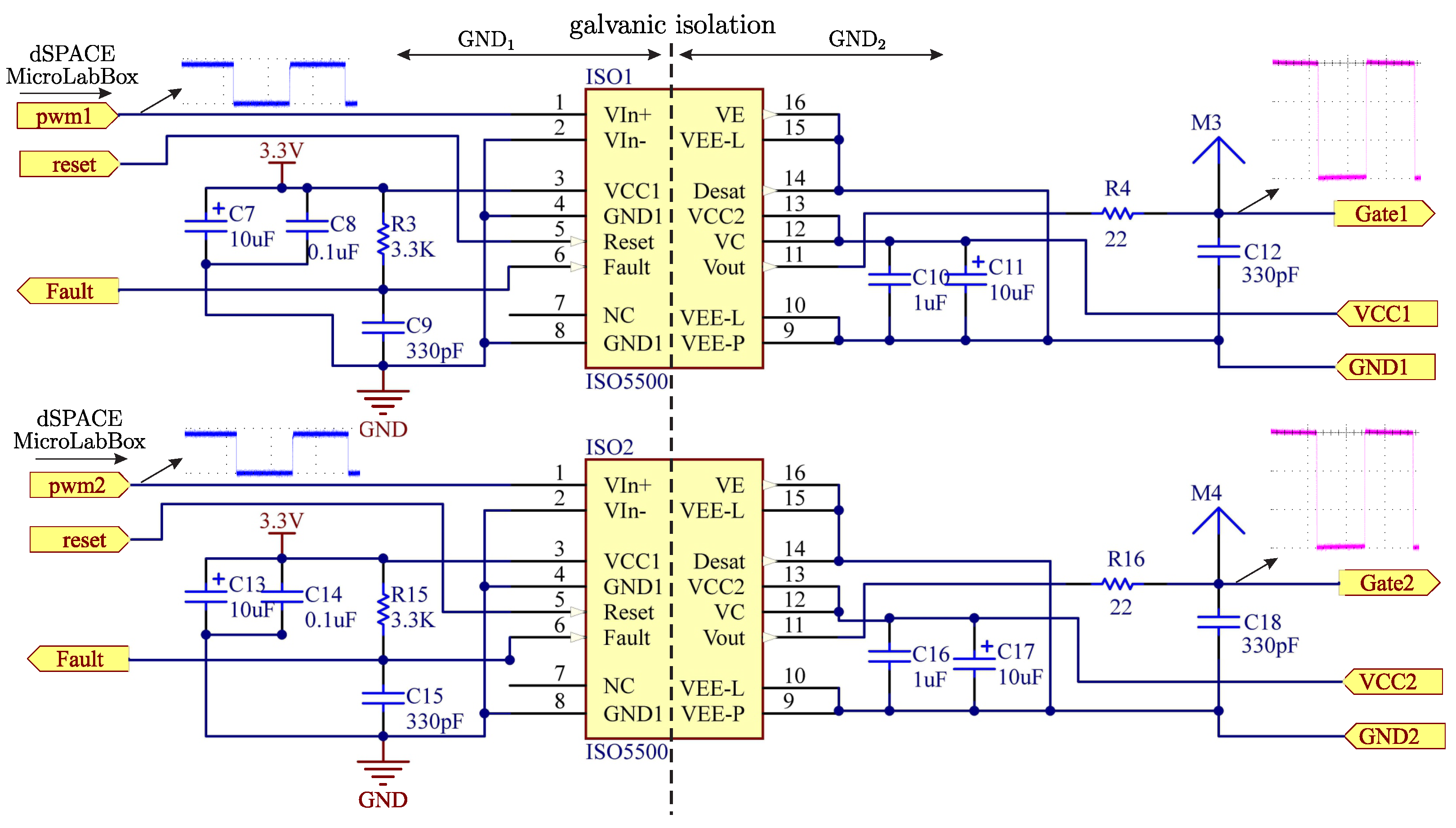
Figure 10a shows the block diagram of the basic Bi-Sw operation. The control module performs signal conditioning for the voltage and current levels (3.3 V to 15 V) required by the power module for the proper operation of its components and electrical noise isolation. The power module is based on the SiC-MOSFET semiconductor device, which essentially works in cut-off and saturation zones at all times, controlling the current flow in both directions. The driver module has been implemented using the ISO5500 device, whose main electrical characteristics are shown in
Table 5. The ISO5500 is a gate driver device for IGBT and power MOSFET semiconductors; it has TTL input and a power output separated by a capacitive isolation barrier. This isolation barrier means that there is separation between the input signal grounds and the power stage, preventing voltage and current noise produced by high switching and power, which can disturb digital control devices. In
Figure 11, the electrical diagram of the driver module is shown. It consists of two main driver devices, ISO5500. The first stage is powered with 3.3 V and has the inputs PWM1 and PWM2, responsible for receiving the control signals from the MicroLabBox control unit. The second stage is fed with VCC1 = VCC2 = 15 V, which corresponds to an output stage and higher power that is responsible for properly biasing the SiC-MOSFETs’ Gate1 and Gate2 outputs, respectively.
Figure 12 shows the evaluations of the module at different switching frequencies.
Figure 12a corresponds to a PWM test signal equal to 5 V/10 kHz input PWM1, and the output response at Gate1 of 15 V peak, measured by oscilloscope probes, is observed. A similar result is presented in
Figure 12b for a signal equal to 5 V/150 kHz, where both experiments show very good responses to high switching frequencies.
The Bi-Sw power module is implemented with a set of SiC-MOSFET (SCH2080KE) power semiconductor devices.
Table 6 shows the main electrical characteristics of the SCH2080KE. The SCH2080KE packages have a built-in anti-parallel diode, which makes it possible for the current to have an alternative path when changing direction. This configuration of power semiconductors results in the formation of a switch capable of blocking voltages and currents in both directions with a wide bandwidth range.
Figure 13 shows the electrical diagram of the Bi-Sw power module with the control signal inputs Gate1 and Gate2 and the power connections J1 and J2, respectively.
5.2. Voltage Source Matrix Converter Experimental Results
VSMC testing is performed using the experimental test bench described in
Figure 10b, where an AC voltage variator is used as an input source and the output balances a three-phase load type
connected in star with values equal to
R = 16
and
L = 10 mH. For this test, the space vector modulation (SVM) strategy is used, in which the 27 valid vectors of the MC are used to obtain a desired output voltage. For the implementation of the SVM, it is necessary to measure the input voltages (
) to the VSMC. The results in
Figure 14 are obtained at a sampling frequency
kHz. In
Figure 14a, the waveforms of the output voltage
and output current
are observed for a reference
= 20 V/60 Hz, and, in
Figure 14b, the same test is performed but for a frequency of
= 20 V/20 Hz. The waveforms of the three-phase output currents are shown in
Figure 14c. The results obtained show correct tracking in the desired reference, and the output currents on the
load present the expected sinusoidal shape.
6. Conclusions
In this article, we have presented a comprehensive approach to the design of VSCs, focusing on three types of converters based on SiC-MOSFET semiconductor devices. We have addressed the limitations of conventional AC-DC-AC 2L-VSCs and explored alternative solutions to improve the overall performance and reliability. Our experimental results have shown the effectiveness of these VSC topologies in various operating conditions, including fault conditions. The parallel operation has provided valuable insights into the behavior and reliability of the converters, demonstrating their robustness and potential for practical applications in cases where a scalable power converter is required. On the other hand, the modular 7L-VSC based on CHB cells has demonstrated its capability to generate sinusoidal voltages and currents with low harmonic distortions at the load side. The modularity of the 7L-VSC based on CHB cells simplifies its extension to higher levels, making it a competitive choice in the new era of VSCs in applications where power quality is required. Furthermore, experimental results show that the VSMC has emerged as a promising solution for direct AC-AC power interfacing without the need for energy storage elements. The utilization of fully controlled bi-directional switches enables the generation of a three-phase sinusoidal voltage with an adjustable amplitude and frequency. The incorporation of SiC-MOSFET semiconductor devices in these converters offers the advantage of higher switching frequencies, contributing to enhanced performance and a reduced size compared to conventional converters.


