Article

Dynamic Analysis of a Supercapacitor DC-Link in Photovoltaic Conversion Applications

1
Dipartimento di Ingegneria dell’Informazione, Università degli Studi di Firenze, 50139 Florence, Italy
2
Dipartimento di Ingegneria Industriale, Elettronica e Meccanica, Università degli Studi Roma Tre, 00146 Rome, Italy
3
Institute of Materials for Electronic and Magnetism-National Research Council (IMEM-CNR), delle Scienze 37/A, 43124 Parma, Italy
*
Author to whom correspondence should be addressed.
Energies 2023, 16(16), 5864; https://doi.org/10.3390/en16165864
Submission received: 15 July 2023 / Revised: 30 July 2023 / Accepted: 5 August 2023 / Published: 8 August 2023
(This article belongs to the Special Issue Advanced DC-DC Power Converters and Switching Converters II)

Abstract

:
In this work, a dynamic analysis describing the charge and discharge process of a supercapacitor for the DC-link between a photovoltaic source and a constant power load is presented. The analysis results in a complete nonlinear and dynamic model that can be used for simulation and control for DC–DC converters, achieving fast recharge times and accurate steady-state voltages in the DC link to avoid overcharging the supercapacitor during low power absorption scenarios. The proposed approach includes parasitic elements for the supercapacitor and efficiency effects on the conversion stage, proposing equations useful for design and control. Stability is also discussed for the charge process of the supercapacitor. Validation of the analytical model is performed by comparison with LTSpice simulation, confirming a good agreement between theory and simulation.

1. Introduction

The power conversion of PV sources for DC and AC applications is almost always required to ensure that their strongly variable voltage and current are regulated in accordance with the electrical and electronic components for which the energy is generated [1,2,3]. This conversion makes use of DC–DC converters that, in general, adapt the voltage for the next stage of conversion (or the final load). This approach is also valid in the case of discrete PV + Storage hybrid systems, where the DC–DC converters are used for matching the output voltage of the solar cell with the charging voltage of the integrated storage device [4]. Since the PV source is a strongly non-linear device based on the photogeneration process [5], it is not only necessary to adapt the voltage to the load, but also to the source, to ensure that the operating point of the PV source is the one where the maximum power is delivered [6,7,8,9]. This process, commonly referred to as maximum power-point tracking (MPPT), introduces the necessity for a dedicated DC–DC converter, since a single converter does not have the degrees of freedom to adapt both input (for MPPT) and output (for correct load functioning) voltage. The two converters, usually connected in cascade, are interleaved with a storage element that has the purpose of stabilizing the voltage and decoupling the converter on the PV side from the converter on the load side. This stage is called the DC-link, and according to the applications, it can be implemented with batteries or capacitors. The former allows the DC-link stage to act as an energy-storage stage, which is particularly useful due to the intermittent nature of the PV source. However, a capacitor-based DC-link is much simpler, leaves less overall footprint, and is more durable [10,11,12,13,14].
The development of new technologies for high-capacity capacitors, known as Supercapacitors (SC), introduced the possibility of achieving a degree of energy-storage capabilities without resorting to a battery-based DC-link. Novel technologies of SC also include interesting results in terms of materials [15], including recycling materials [16] and natural and organic sources [17,18]. SC offers acceptable energy density (albeit still lower than Li-based batteries) with very high-power density. SCs are also less expensive and age much less quickly due to their charge and discharge patterns.
Unfortunately, the electrical behavior of a SC is different from a battery’s, also due to the variable voltage across its terminal as dependent on the state of charge [19,20,21]. A battery exhibits an almost constant voltage across its terminals for the majority of its discharge (and charge) process. SC behavior is similar to a that of a classic capacitor, and thus, in the best of cases, discharges exponentially. Although the decoupling capabilities of the SC are ensured, the voltage range that it exhibits during operative conditions is large, and this requires special care in the control of the DC–DC converters, especially the one connecting the SC to the non-linear PV source.
The purpose of this work is to investigate the dynamics of the SC in an energy-conversion chain, starting from a PV source and ending with a constant-power load, which is a very common DC load able to support, for example, USB powered devices. To investigate the dynamic of the system, a circuit model of the chain, representing the conversion at frequencies below the ones of the dynamic response for the converter but including the ones regulating the charge and discharge processes of the SC, is proposed [22,23]. The model includes the non-linear nature of the PV source, the efficiency of the converter distributed among voltage and current drops, and both ideal and parasitic models for the SC.
With respect to current research, the novelty of this work contribution is twofold. First, an analytical complete dynamic model including parasitic components is presented for a very actual scenario of low–mid power generation from renewable sources. The investigation of this model highlights novel results such as the feasible operating ranges for the charge operation of the DC-link supercapacitor, determining stable and unstable equilibrium points of the dynamic system. Second, a numerical approach to estimate the duty cycle for the final-voltage charge is presented, considering the full non-linear nature of the photovoltaic source. Moreover, both results are validated against LTSpice time-domain simulations, considering both the low-frequency DC model of the power conversion stage and its fully dynamic high-frequency implementation. All LTSpice models are reported in their completeness for repeatability of the proposed study. The analytical and numerical analysis presented can be used as a foundation for advanced control algorithms and energy-storage management systems.
The manuscript is structured as follows. First, the energy conversion chain will be described, and individual circuit models will be proposed for the block constituting it. Then, according to the parasitic model considered in the SC, three different state–space models for three different chains are derived. Then, feasibility regions for the final voltage charge are discussed, and the numerical problem to derive the duty-cycle is formalized and solved. Following, the validation procedure in the LTSpice environment is presented along with the simulation results. Final remarks and a conclusion close the manuscript.

2. Materials and Methods

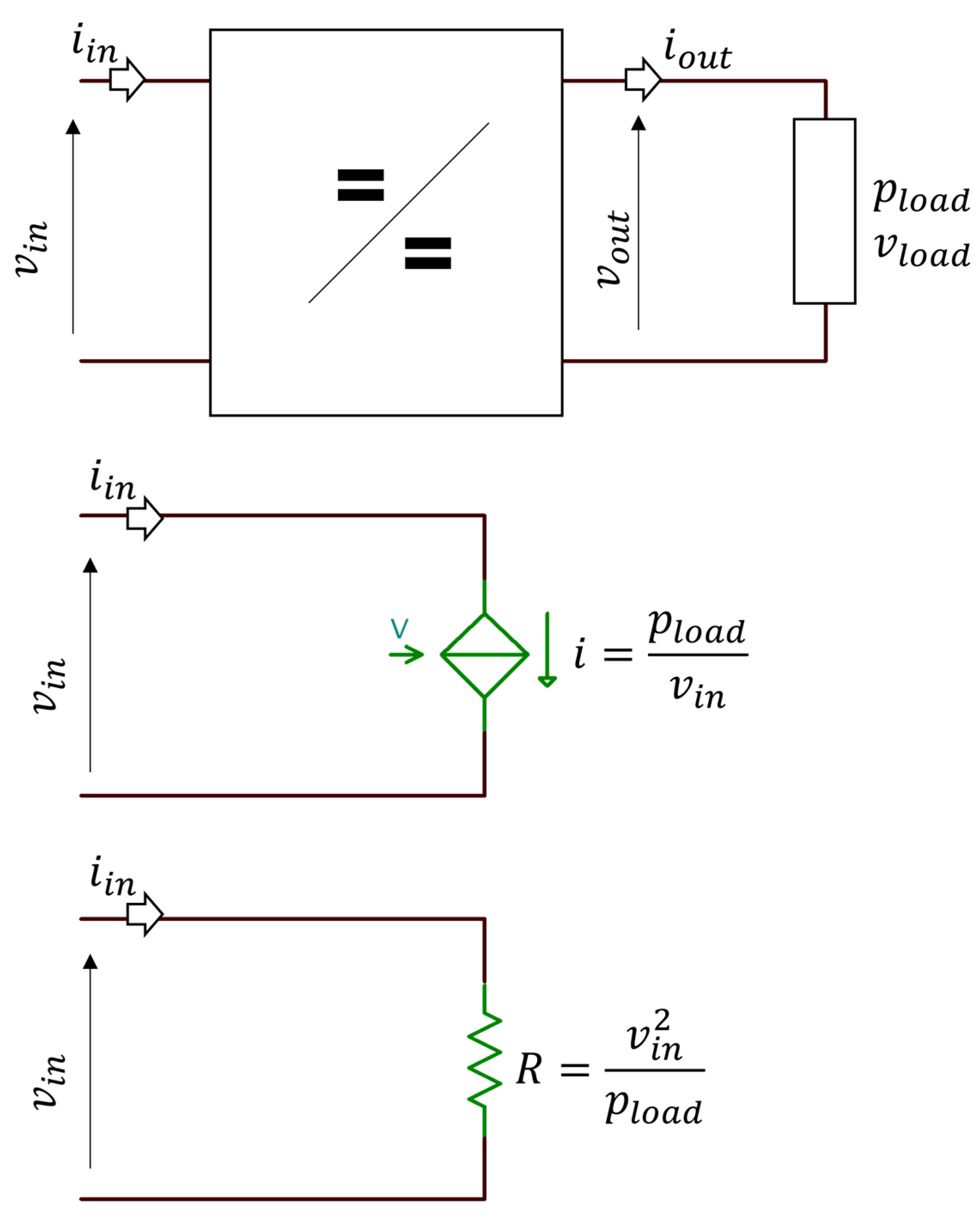
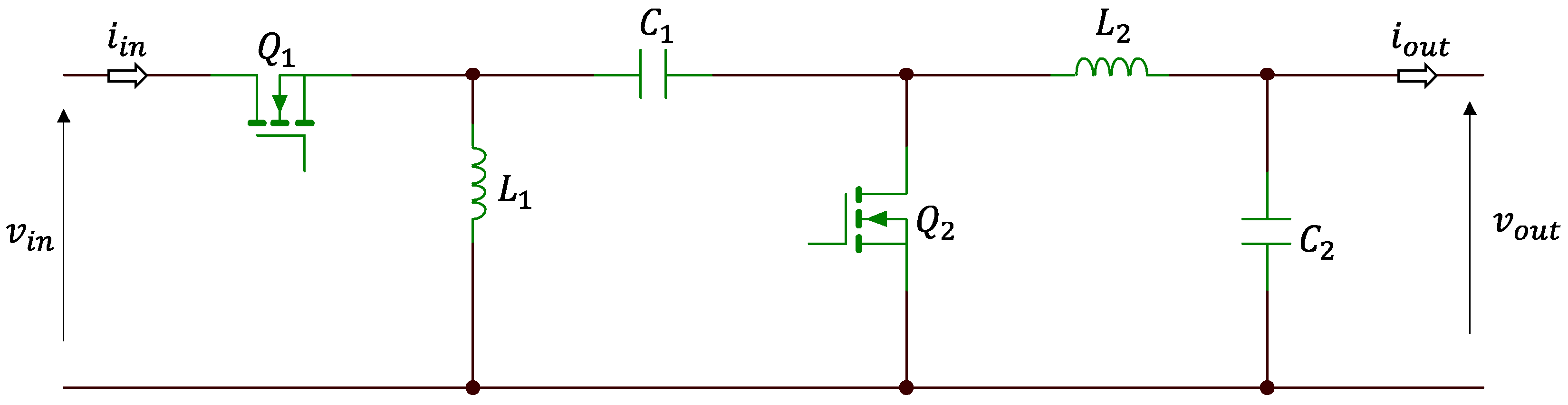
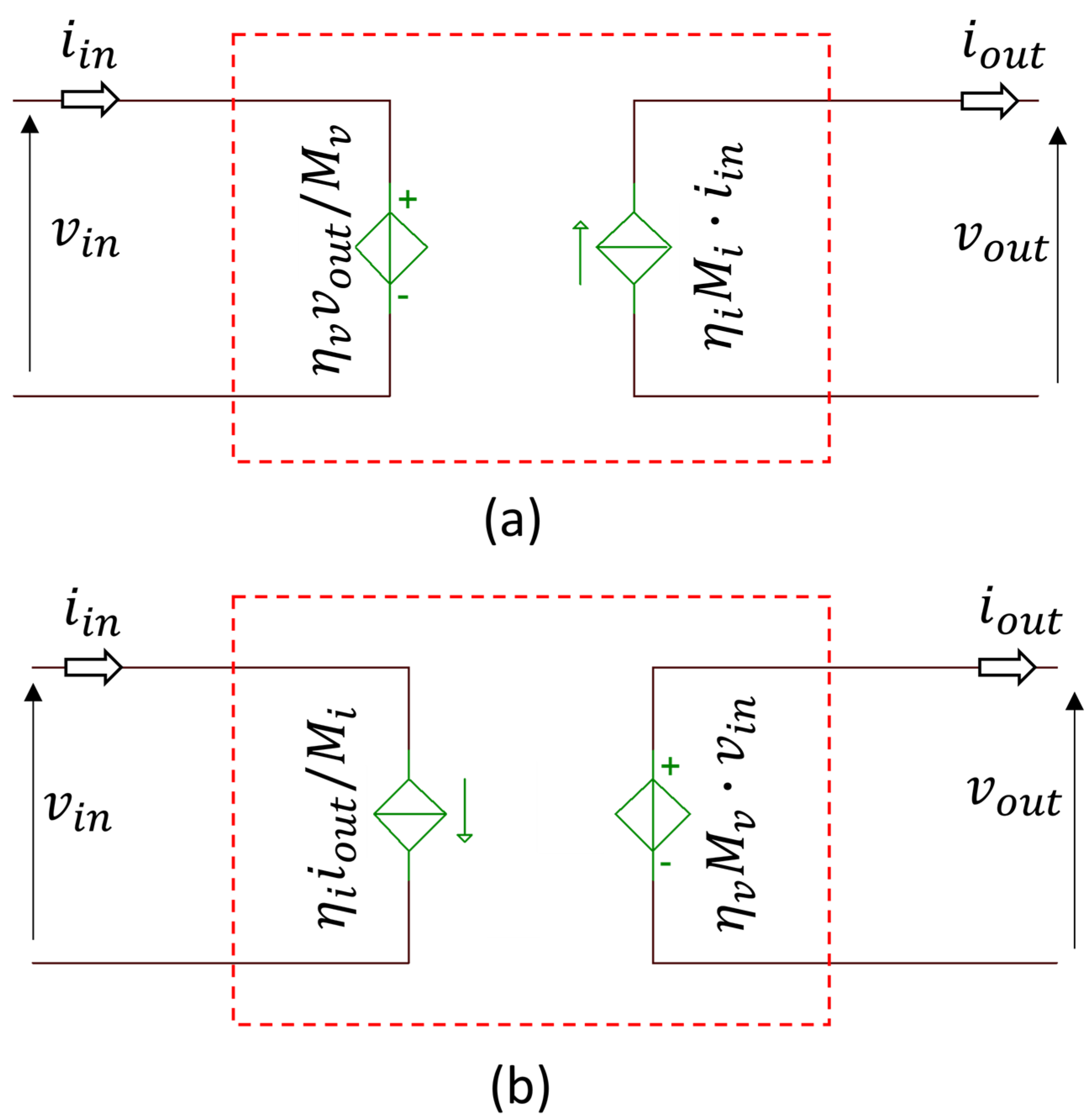
2.1. Modelling for the Blocks of the Conversion Chain

The energy-conversion chain considered in this work is composed of five blocks. The first block is the primary source of energy, represented by a generic PV device under variable conditions of irradiance and temperature. The second block is the first DC–DC converter, operating to regulate the energy conversion between the PV source and the following DC-link supercapacitor. The third block is the supercapacitor itself, which features a capacitance and operating voltage range according to the design of the remainder of the system. The fourth block is the second DC–DC converter, operating to regulate the energy conversion between the DC link and the final load. The fifth block is the load itself, which is assumed as a CV&CP load (constant voltage and constant power). Each individual block of the conversion chain can be represented by a suitable circuit model that can later be coupled to achieve a full dynamic representation of the system.
For the first block, the equivalent circuit model known as “single diode” or “one diode” is used to represent the behavior of the photovoltaic source. The model is lightweight and can be used to represent a large variety of silicon-based PV sources and other technologies [24], and the process for the identification from experimental data or the produced datasheet values is well understood in the literature [25]. The model-circuit representation is given in Figure 1.
The model drawback is the implicit nature of its current-voltage relationship, which is given by (1):
i p v = I i r r I o e v p v + R s i p v n V T 1 v p v + R s i p v R s h
where  I i r r  is the photogenerated current,  I o  is the reverse saturation current of the diode,  n  is the modified quality factor of the diode,  R s h  is the shunt resistance and  R s  is the series resistance. The  V T  term represent the thermal voltage ( 26   m V  at  293.15   K ). The five parameters { I i r r , I o ,   R s ,   R s h , n } can be identified in specific irradiance  G  and temperature  T  conditions addressed in literature as Standard Test Conditions (STC). The conditions are  G = 1000   W / m 2  and  T = 293.15   K . Individual equations are reported in the literature to calculate the parameters in conditions different from STC.
The current-voltage relationship shown in (1) can be used in practical applications through numerical methods that calculate the current  i p v  given a known voltage  v p v , or vice-versa. However, the numerical solution of (1) is not practical if, for example, the PV device should be included in Kirchhoff Voltage Laws (KVL) or Kirchhoff Current Laws (KCL) for formulating state-space equations. In this case, an alternative formulation can be used, which exploits the Lambert-W function to give an explicit expression of  v p v  as a function of  i p v  (2) and  i p v  as a function of  v p v  (3).
v p v = R s h I i r r + I o R s + R s h i p v n V T W I o R s h n V T e R s h I i r r + I o i p v n V t
i p v = n V T R s W R s n V T · I o R s h R s h + R s · e R s h R s + R s h v p v + R s I i r r + I o n V t + I i r r + I o R s h v p v R s h + R s
The formulation with (2) and (3) are explicit and can be implemented easily in KVL and KCL. Indeed, the formulation is still numeric, but the computational burden is moved from the generic root-finding that is present in (1) to the solution of the Lambert-W, which can be optimized and is in general an easier task. Equations (2) and (3) provide a complete electrical characterization of the first block and can be completed with update equations for the parameters to account for variable irradiance and temperature conditions [26,27,28].
The second block is represented by the first DC–DC converter. The role of this converter is to set the operating point of the PV device to ensure proper current flowing inside the DC-link. In general, if the DC-link is implemented by means of a SC, its voltage should be low. For this reason, a step-down converter could be used to convert the voltage from the PV source to the SC. However, this could limit the operating conditions of the PV device in the case of smaller systems. On the other hand, step-up-down topologies such as the SEPIC or Zeta converters can be implemented with very little effort and offer large voltage gains with high efficiency. The Zeta converter topology is the one considered for this block and is shown in its ideal lossless representation in Figure 2. The Zeta converter is a topology particularly suitable for photovoltaic (PV) applications due to several advantages. It can achieve a high voltage gain, making it suitable for boosting the low voltage output of PV panels to the desired level. This is especially useful when the PV array operates at low voltage levels, as it allows efficient energy conversion without the need for additional voltage-boosting stages. Unlike the Boost converter, which typically requires multiple stages for voltage conversion, the Zeta converter can perform the voltage step-up or step-down conversion in a single stage. This simplifies the converter topology, reduces the component count, and improves overall efficiency. Finally, the Zeta converter is capable of accommodating a wide input-voltage range, allowing it to handle the fluctuations in the PV panel output more effectively [29,30,31,32].
The complete derivation and sizing for the converter can be found in the literature. Under the assumption of continuous-conduction mode (CCM), the converter-voltage gain and current gain in steady state can be approximated as:
M v = v o u t v i n = D ( 1 D )
M i = 1 M v
where  M v  is the lossless voltage gain,  M i  is the lossless current gain, and  D  is the duty cycle for which the Q1 transistor is in conduction and the Q2 transistor is in interdiction. In case lossy elements are present in the converter, the efficiency is in general distributed between the voltage and current gain, since:
η = v o u t · i o u t v i n · i i n = M v , l · M i , l = η v M v · η i M i
where  η  is the efficiency of the converter and  M v , l  and  M i , l  are the lossy voltage and current gain. The distribution of the efficiency  η  as the scaling terms  η v  and  η i  depends on the specific values of the parasitic components. Equations (4)–(6) yield a simple steady-state representation of the converter through two mutually-coupled controlled generators, as shown in Figure 3a.
Indeed, a reciprocal representation with the current generator on the primary side and the voltage generator on the secondary side is possible as well, as shown in Figure 3b. Both representations are correct and allow the formulation of KVL/KCL. The choice of one over the other for formulation resides in the representation of the third block.
Under the reasonable assumption that the DC–DC converter operates to achieve Maximum Power Point Tracking (MPPT) on the PV device, the voltage gain will be set as:
η v M v = v o u t v m p ;       η v 1 M i = v o u t v m p ;       M i = v m p v o u t η v
where  v m p  is the voltage where maximum power is exhibited by the PV source. Indeed, a reciprocal approach could be taken in case of imposing the current gain, albeit much less common. The third block is the DC-link, which is constituted by a SC. The SC can be represented by a capacitor with a capacitance C and a variable degree of parasitic elements. The simpler representation shown in Figure 4a is a simple, lossless capacitor. Inclusion of a parallel self-discharge resistor,  r s h , is shown in Figure 4b. Inclusion of an additional equivalent series resistance (ESR),  r s , is shown in Figure 4c, which constitutes the complete, lossy representation of the SC.
Where  i b ( t )  is the branch current, the behaviour of the SC in the three represented equivalent circuits can be determined by the following state equations:
v ˙ c t = 1 C i b ( t )
v ˙ c t = 1 C i b t v c t r s h
where (8) can be used for Figure 4a and (9) can be used for Figure 4b,c. The presence of the  r s  element does not directly alter the state equation but influences the branch current according to how the element is connected to the rest of the circuit.
The fourth and fifth blocks operate in a coupled mode: since the load is expected to operate at a constant voltage  v l o a d  for variable absorbed power  p l o a d , the secondary DC–DC converter operating the conversion between the DC-link and the load must be controlled to ensure that the output voltage  v o u t  is always equal to  v l o a d .
To ensure  v o u t = v l o a d , the voltage gain of the converter is:
M v = v l o a d v i n
If the load must operate with  p l o a d  and  v l o a d , regardless of its inner nature, the absorbed current will be  i l o a d = i o u t = p l o a d / v l o a d . Assuming the converter operates, for simplicity, with unitary efficiency  η = M v M i = 1 , the output current seen from the primary side of the load is:
i i n = i l o a d M i = i l o a d · M v = i l o a d · v l o a d v i n = p l o a d v i n
R = p l o a d v i n 2
Thus from (9) it is possible to derive a representation as a controlled generator, and from (10) as a voltage-controlled resistor. Clearly, both representations are non-linear elements. The three representations are shown in Figure 5.

2.2. Full Chain Dynamic Model

Full modeling of the dynamic system should take into account both the interaction between the DC–DC converter and the storage elements [33,34,35] and between the DC–DC converter and the photovoltaic source [1,36,37,38,39]. Also, the model must implement a current sink for a constant power load operating at a specific desired voltage, such as the case for a USB powered device [40,41]. The proposed model taken individually exhibits a different dynamic behavior from the one shown in the full-chain dynamic model presented hereafter. The most notable difference is that the concurrence of a power-limited nonlinear source such as a PV device with a constant power load creates a non-feasible area where, even if the theoretical maximum delivered power by the PV device is higher than the power required by the load, the SC will not charge unless an appropriate MPPT strategy adapting the operating point is implemented.
Since the only dynamic element present is the capacitance in the SC block, the system behaves as a non-linear first-order system. Thus, its dynamics should be described from the complete state-equation describing the voltage across the capacitor. According to the representation of the SC block, different equations or sets of equations must be considered.

2.2.1. Ideal Supercapacitor Dynamic Model (IDSC)

In this case, the SC is represented without any parasitic component. A simple explicit state equation can be formulated as following:
v ˙ c = 1 C η i M i i p v v c η v M v p l o a d v c
where the term  i p v [ v p v ]  is given by (3). Under the assumption that the converter operates in MPPT according to Equation (7):
v ˙ c = 1 C η i M i i p v v m p p l o a d v c
v ˙ c = 1 C η i v m p v o u t η v i m p p l o a d v c
v ˙ c = 1 C η p m p p l o a d v c
Interestingly, the state equation can be solved analytically leading to the time expression of the capacitor voltage. From a known initial voltage  v c ( 0 ) :
v c t = ± 2 · t · [ η p M P p U S B ] C + v c 0 2

2.2.2. Self-Discharge Supercapacitor Dynamic Model (SDSC)

The derivation in this case is very similar to the IDSC one, since the only difference is the presence of an additional term in the state equation describing the branch current.
v ˙ c = 1 C η i M i i p v v c η v M v p l o a d v c v c r s h
v ˙ c = 1 C η p m p p l o a d v c v c r s h
The main difference resides in the presence of an additional term relative to the current flowing on the shunt resistance. The solution in this case is a superposition of the previously found solution with a discharge exponential.

2.2.3. Full Supercapacitor Dynamic Model (FSC)

In this case, the voltage across the supercapacitor is different from the voltage across the output of the first DC–DC converter, and this difference depends on the current drawn from the PV source. This results in an implicit-state equation that must be solved in conjunction with a KCL to derive the branch current on the supercapacitor.
v ˙ c = 1 C η i M i i p v p l o a d v c η i M i i p v η v M v v p v v c r s p l o a d v c v p v i p v v p v = 0
The system can only be integrated numerically, deriving at each time-step the  v p v  voltage and  i p v  current from the last two equations, and substituting the  i p v  in the first-state equation to compute (e.g., thorough Euler or Runge–Kutta integration) the next timestep value of the capacitor voltage.

2.3. Equilibrium Points for Final Voltage Charging

In practical applications, the produced power from the PV source will be larger than the power drawn from the load. Assuming perfect MPPT, this leads to an unstable system without equilibrium points, where the voltage across the capacitor rises indefinitely. In particular, the square-root-of-time expression in (17) represents the fastest possible charging velocity that can be achieved in this system.
In real scenarios, however, this charge curve must be abandoned when in proximity of the SC maximum voltage to avoid damaging the component. In this case, a voltage gain (and thus, a duty-cycle) for the primary DC–DC converter must be determined with the aim of creating an equilibrium point for the SC voltage equal to the SC nominal maximum voltage  v c = v M A X .
Let us first consider the IDSC chain with  η = 1 . The equilibrium point to be found is the one where the current drawn from the load  p l o a d / v M A X  is equal to the current coming from the converter  η p m p / v M A X . This is an operating condition where this equilibrium for a possible  M v ,   M i  can be better explained graphically. In Figure 6, several I–V characteristics of a 54 W PV source are represented, as seen from the secondary side of the first PV panel, for different  M v ,   M i  gains. The thick, black line is the IV characteristic at  M v = M i = 1  (thus equal to one of the PV devices). The red and blue crosses represent four combinations of loads (imposing the  p l o a d ) and SC (imposing the  v M A X ), as reported in Table 1. The dashed line represents the ensemble of the maximum power points.
Figure 5. Fourth and fifth block: a constant voltage with a variable absorbed power load and a DC–DC converter. Below, the primary side representations of the load.
Energies 16 05864 g005
As can be seen from the figure, the two blue combinations fall within the possible operating points that can be determined on the secondary side of the first DC–DC converter, whereas the red combinations are not. In a lossless and completely ideal chain as the IDSC with  η = 1 , an equilibrium point is always found as long as  p l o a d < p m p .
Relaxing the condition on the efficiency, three possible scenarios can be studied: efficiency is distributed among voltage and current gain  η = η v η i , efficiency is negligible on the current gain  η = η v  and efficiency is negligible on the voltage gain  η = η i . The result is shown in Figure 7a–c.
The dashed black line represents the ensemble of the maximum power points for  η = 1 , kept as a reference. As can be seen, the voltage and current distribution of the efficiency strongly alters the lieu of feasible operating points that can be obtained at the secondary side of the first DC–DC converter. An even distribution of efficiency for voltage and current in Figure 7a shifts the ensemble towards the origin, slightly limiting both maximum voltage and current. A distribution of efficiency skewed towards voltage or current limits, respectively, the maximum voltage and maximum current. Due to the effect of efficiency, previously feasible combinations of  p l o a d ,   v M A X  can fall outside the lieu of operating points.
The introduction of the non-ideality in the SC stage consists in using the SDSC or the FSC chain instead of the IDSC. The inclusion of SDSC results in an additional current to consider, the one absorbed by the load. This current is  r s h / v M A X  at the equilibrium. Thus, this shifts the operating points “upward” in the I–V plots shown before. A simple example is given for the  η = 1  case, where an  r s h  resistance with range  r s h = 10 1000   Ω  is considered (note that this range is highly unrealistic for an SC, but it is useful for visualization purposes). As could be expected, the effect of self-discharge is more present for higher  v M A X  values (Figure 8).
However, it should be noted that the equivalent self-discharge resistance for series-connected SCs decreases for each added cell; thus, in practical cases, this effect is independent of the  v M A X . Finally, the FSC chain behaves in the same manner as the SDSC chain. This is due to the positioning of the  r s  element, which does not alter the KCL used to study the SDSC.

2.4. Duty Cycle for Final Voltage Charging

In the previous, the IDSC, SDSC and FDC chains were analyzed to understand whether, given a couple of  p l o a d ,   v M A X , a combination of voltage and current gain could be found that would ensure that the SC would have  v c = v M A X  at equilibrium. In this section, the strategy to determine the gains (and the relative duty-cycles) are discussed.
The desired gains are the ones that ensure:
v ˙ c = 1 C η i M i i p v v M A X η v M v p l o a d v M A X = 0 I D S C 1 C η i M i i p v v M A X η v M v p l o a d v M A X v M A X r s h = 0 S D S C 1 C η i M i i p v v M A X η v M v · r s + r s h r s h p l o a d v M A X v M A X r s h = 0 F S C
Albeit the current across the capacitor is null, in this case, the optimal gain value is different between SDSC and FSC due to the (in general negligible) voltage divider term.
Regardless of the specific chain, (21) expresses a numerical problem in the two unknowns  M v , M i . Since those are the lossless gains, and  M v = 1 / M i , the problem can be reduced to a single unknown. Expressing the voltage gain as  M v = D 1 D ,  it is possible to rewrite (21) as a set of equations in D for which the zero corresponds to a duty-cycle leading the SC to charge at  v M A X .
f I D S C D ,   v M A X , p l o a d = η i 1 D D i p v 1 D D v M A X η v p l o a d v M A X
f S D S C D ,   v M A X , p l o a d = η i 1 D D i p v 1 D D v M A X η v p l o a d v M A X v M A X r s h
f F S C D ,   v M A X , p l o a d = η i 1 D D i p v 1 D D v M A X η v · r s + r s h r s h p l o a d v M A X v M A X r s h
Any one of equations in (22)–(24) can be equaled to zero and solved numerically (using (3) for the current-voltage relationship) for different values of  p l o a d  and  v M A X  to determine the desired duty cycle D. In general, for a given Equations (22)–(24), and a specific  p l o a d  and  v M A X , there are two numerical solutions to (22)–(24). This is because a given current, leading to equilibrium, can be achieved both in the near open-circuit area of the PV converter and near the short-circuit area of the PV converter, as seen in similar previous works [42]. Visualization of the solutions for (22)–(24) requires some constraints, since considering the variable D and the two parameters  p l o a d  and  v M A X  results in a three-dimensional function for which the zero-crossing cannot be visualized. Thus, in the following plots, the  p l o a d  will be assumed as constant. In Figure 9a, the absolute values of the  f I S D C  are shown for a  p l o a d < p m p . Then, to compare the magnitude of the variations among the different (22)–(24), in Figure 9b a cross-section of the surface for  v M A X = 6   V  is shown also for  f S D S C  and  f F S C . In this case, series  r s = 1   Ω  and shunt  r s h = 50   Ω  resistances were considered in the SDSC and FSC cases. Again, the quantities are elevated for visualization purposes, but it is relevant to understand that very little difference occurs at a steady state between the purely ideal IDSC case and the parasitic-affected SDSC and FSC cases. The two solutions are not both stable. In fact, the sign of the  v ˙ c  can be studied to derive a phase portrait shown in Figure 10, where it can be seen that the equilibrium points found for higher  D  and lower  v M A X  are a boundary towards an unstable region where the SC will simply discharge to zero instead of reaching the equilibrium point. In practical terms, since the low boundary of D is often limited by design, this creates a minimum voltage for the SC below which there is no way to recharge it anymore.

3. Validation Results

The methodology and the equations proposed herein are validated through a time-domain simulation of the IDSC, SDSC and FSC chains in an LTSpice environment. The schematic is depicted in Figure 11. As can be seen, the PV source can be implemented using an ideal diode specifying the N and Is parameters. The PV device implemented in the figure delivers a power of  p m p = 47   W  at  v m p = 16.6   V . The conversion stage is implemented via controlled generators, including the efficiency already divided in the current and voltage contribution. The SC link is represented in the FSC form with parametric resistances which can be set at very high (shunt) and low (series) values to restore the semi-ideal SDSC or the fully ideal IDSC chains. The load is represented by a current generator operating at constant power. It should be noted that this behavioral source rolls back to a pure resistor if the voltage across it falls below a certain threshold, to avoid divergence during simulation.

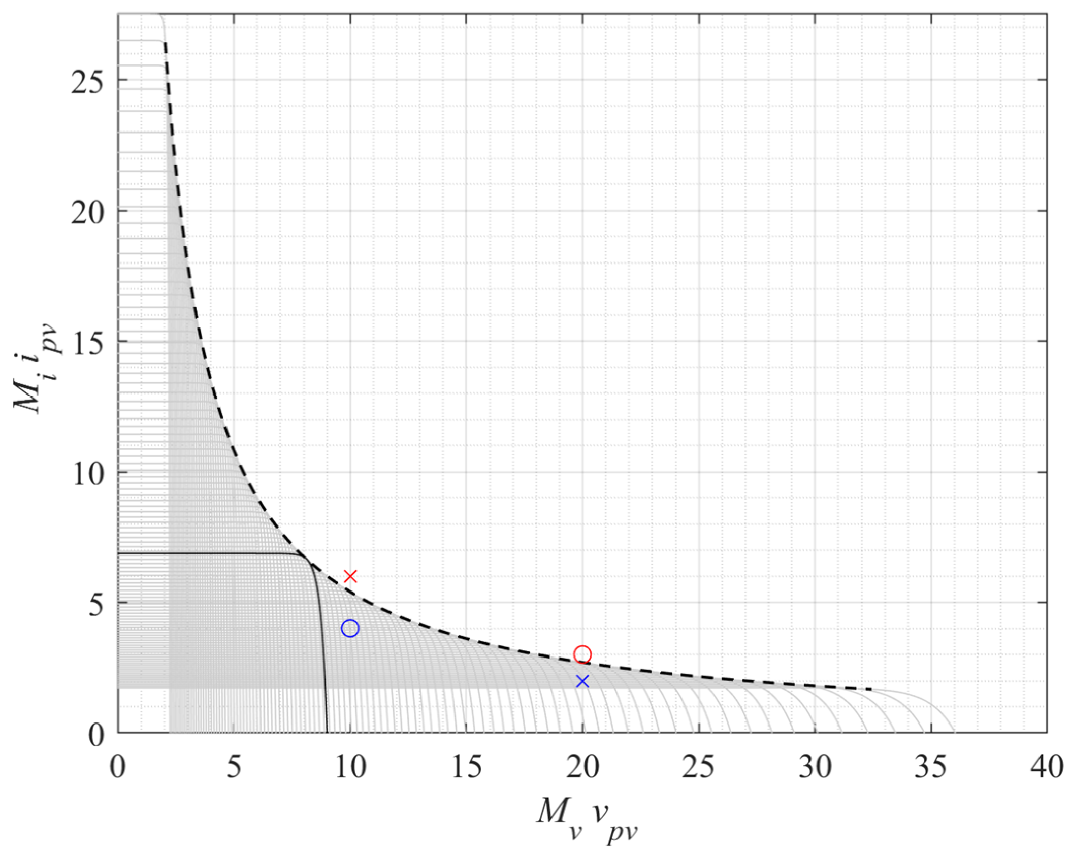
3.1. Test A: Final Voltage Charge and Stability Region

In this test the SC is initially kept at a variable charge between 2 V and 16 V. The charging is performed at a fixed duty-cycle (D = 0.6), and the load absorbs a constant power of  p l o a d = 20   W . The final voltage and the equilibrium points delimiting, for D = 0.6, the stability region, are computed with (24). The charging profiles are shown in Figure 12 (left) along with the vertical aligned  | f F S C |  in Figure 12 (right). Confirming the hypothesis, the SC charges (or discharges) towards the equilibrium point as long as the initial condition is within the stability region shown in green. If it falls below, in the region shown in red, it will simply discharge to zero. The slight difference in the equilibrium points (less than 0.5 V) can be attributed to the different model used by the diode in LTSpice.

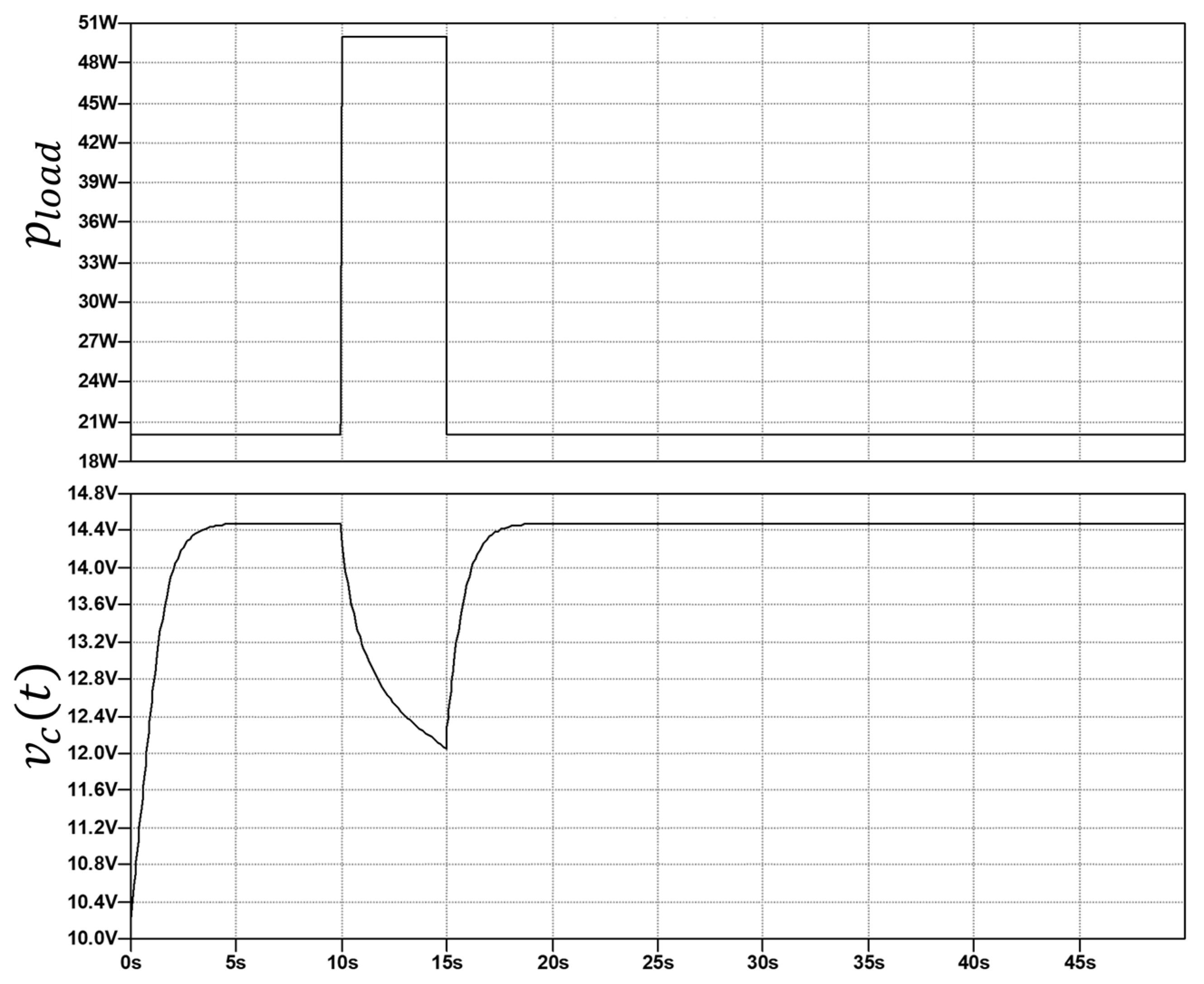
3.2. Test B: Short and Heavy Load Perturbation

In this test, the chain initially works at a nominal load  p l o a d = 20   W ,  and the SC is charged to the final value (initial value is 10 V). After it reaches the charged state, a heavy and short (5 s) load perturbation is applied. The load is incremented by 300% to  p l o a d = 50   W , thus driving the system outside the feasible area. As can be seen, the voltage across the capacitor drops rapidly, and if the perturbation were to continue indefinitely, it would reach zero as expected. Time-domain simulations are shown in Figure 13.

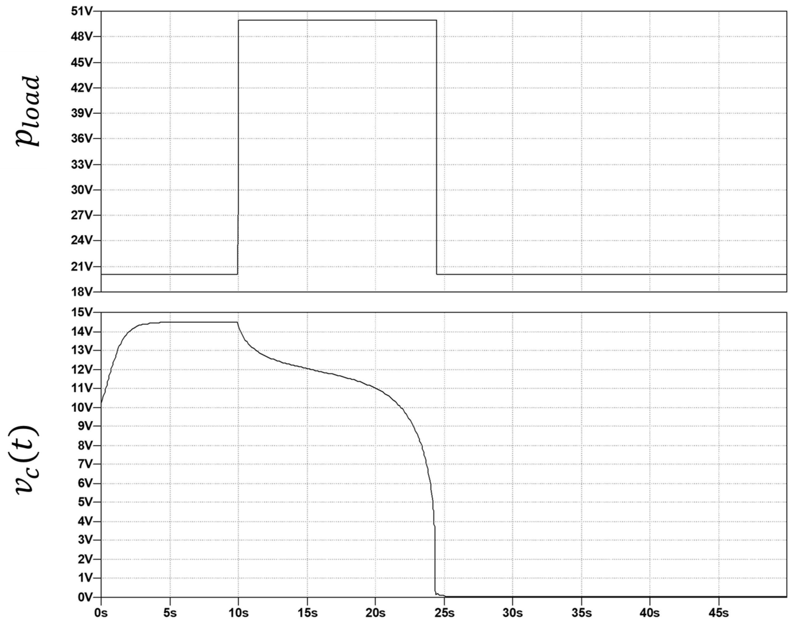
3.3. Test C: Long and Heavy Load Perturbation

This test is similar to the previous one, but in this case, the perturbation from the nominal condition ( p l o a d = 20   W ) is going to be longer (15 s). The notable difference that can be appreciated is that the discharge induced in the capacitor by the load perturbation leads the SC in the unstable region; thus, even after the perturbation has ended, the SC is not able to recover and simply discharges to zero as expected. Time-domain simulations are shown in Figure 14.

3.4. Test D: Dynamic Response

This test compares the adynamic response of the chain, where the only dynamic element is composed by the SC, with the fully dynamic response of the circuit with a properly sized Zeta converter. The converter was sized to ensure a CCM for D = 0.5 and an operative switching frequency of 10 kHz. The LTSpice model of the dynamic converter is shown in the top part of Figure 15, and the comparison of the voltage waveforms between the adynamic previous results and the dynamic measured ones can be seen in the bottom part of Figure 14. As can be seen, the charging dynamics are slightly different in the dynamic case (as the transfer function of the dynamic converter influences the time-domain response), but the steady-state value is practically identical. Moreover, the same considerations concerning the stable and unstable regions are still valid in the dynamic time domain analysis.

4. Discussion

The proposed model, the insight derived from its analysis, and the validation obtained from the simulations are useful tools to understand the possibilities that are available for a SC-based DC-link in the very common application of PV conversion for constant power loads. The dynamic-state equations derived in Section 2 are validated against time-domain simulations, offering an accurate and computationally lightweight alternative for time-domain simulation of these kinds of systems in environments that do not natively implement circuit simulation.
The estimation of the feasible region for the final-voltage charge with different distribution of the efficiency towards voltage and/or current highlights the necessity of deeper consideration when analyzing power converters. In fact, most of the analysis assumes a resistive load (for which the efficiency skewness is irrelevant), but for non-linear applications such as the one proposed in this manuscript, the effects of voltage and current drop are dramatically different. Since this contribution comes from different parasitic elements inside the converter, a possible evolution of this work is to consider the correlation between such parasitic elements and the shrinking of the feasible area.
The study of the stable and unstable regions opens a discussion on the possible operating conditions where the system can or cannot operate. In fact, operating in the unstable region leads to a discharge of the SC. The minimum possible duty-cycle supported by the converter creates a lower boundary for the SC voltage, thus limiting in fact the available energy that can be extracted from it. This is not necessarily a very limiting factor, since many modern SC technologies, such as the hybrid SC [14], are already lower-bound limited in voltage, yet the consideration of this boundary is at this point critical during the design stage of the system. It turns out from the simulations that the proposed voltage-conversion system equipped with an SC-based DC-link is very effective in the case of constant power loads (as in the case of resistive loads or battery storage devices). However, the effectiveness and stability of this system are highly dependent on the initial charging conditions of the SC, which must exhibit a starting voltage above a certain threshold to be charged under stability conditions. In order to avoid unstable working conditions, it would be more effective to use hybrid SCs with a minimum starting voltage [20] in the DC-link section, or to associate standard SC’s with an undervoltage protection circuit.

5. Conclusions

In this work, a fully dynamic model for the conversion chain between a photovoltaic source and a constant power load with a supercapacitor-based DC-link is proposed. The system was studied considering the circuit model, including the non-linear nature of the PV source, the efficiency of the DC–DC converter, and the parasitic elements on the supercapacitor model. The study investigated the dynamic nature of the system, highlighting critical aspects such as a bounded region of feasibility for the charge of the SC element and the presence of a stable and unstable set of equilibrium points leading to a final-voltage charge. The proposed approach offers a valuable tool for implementation of control algorithms, further refinement of the analysis by considering the DC–DC converter individual parasitic components, and development of MPPT strategies incorporating both the non-linear nature of the PV source and the dynamic behavior of the DC-link stage. Validation in terms of hardware full-chain implementation or through hardware-in-the-loop approaches constitutes the future development of this work. Concerning the converter, a practical approach for the converter implementation can be found in [43]. Concerning the implementation of the storage, interesting results to be investigated can be found in [44], and, in a completely passive PV and battery configuration, in [45]. It should be noted, however, that as shown in this work, the converter efficiency plays a major role in the general performance of the system, and for this reason, efficient and isolated converters operating at high frequency could be the best choice [46].

Author Contributions

Conceptualization and Methodology, G.M.L., M.Q. and A.L.; resources and project administration, S.R. and F.P.; Software and Validation, G.M.L. and F.C.; investigation and formal analysis, M.P., A.L. and F.C.; supervision, A.L. and S.R. All authors have read and agreed to the published version of the manuscript.

Funding

This work was partially funded by the Italian Ministry of University and Research: “Ecosystem for Sustainable Transition in Emilia-Romagna” (Ecosister), funded under the National Recovery and Resilience Plan (NRRP), Mission 4 Component 2 Investment 1.5-Call for tender No. 3277 of 30 December 2021.

Data Availability Statement

Data and simulations are available at readers’ requests.

Conflicts of Interest

The authors declare no conflict of interest.

References

  1. Corti, F.; Laudani, A.; Lozito, G.M.; Reatti, A. Computationally efficient modeling of DC–DC converters for PV applications. Energies 2020, 13, 5100. [Google Scholar] [CrossRef]
  2. Azuatalam, D.; Paridari, K.; Ma, Y.; Förstl, M.; Chapman, A.C.; Verbič, G. Energy management of small-scale PV-battery systems: A systematic review considering practical implementation, computational requirements, quality of input data and battery degradation. Renew. Sustain. Energy Rev. 2019, 112, 555–570. [Google Scholar] [CrossRef] [Green Version]
  3. Sri Revathi, B.; Prabhakar, M. Non isolated high gain DC–DC converter topologies for PV applications—A comprehensive review. Renew. Sustain. Energy Rev. 2016, 66, 920–933. [Google Scholar] [CrossRef]
  4. Fagiolari, L.; Sampò, M.; Lamberti, A.; Amici, J.; Francia, C.; Bodoardo, S.; Bella, F. Integrated energy conversion and storage devices: Interfacing solar cells, batteries and supercapacitors. Energy Storage Mater. 2022, 51, 400–434. [Google Scholar] [CrossRef]
  5. Imran, A.; Zhu, Q.; Sulaman, M.; Bukhtiar, A.; Xu, M. Electric-Dipole Gated Two Terminal Phototransistor for Charge-Coupled Device. Adv. Opt. Mater. 2023, 2300910. [Google Scholar] [CrossRef]
  6. Laudani, A.; Lozito, G.M.; Lucaferri, V.; Radicioni, M.; Fulginei, F.R.; Salvini, A.; Coco, S. An analytical approach for maximum power point calculation for photovoltaic system. In Proceedings of the 2017 European Conference on Circuit Theory and Design, ECCTD 2017, Catania, Italy, 4–6 September 2017. [Google Scholar]
  7. Kumar, N.; Hussain, I.; Singh, B.; Panigrahi, B.K. Self-Adaptive Incremental Conductance Algorithm for Swift and Ripple-Free Maximum Power Harvesting from PV Array. IEEE Trans. Ind. Inform. 2018, 14, 2031–2041. [Google Scholar] [CrossRef]
  8. Chiang, S.J.; Shieh, H.J.; Chen, M.C. Modeling and control of PV charger system with SEPIC converter. IEEE Trans. Ind. Electron. 2009, 56, 4344–4353. [Google Scholar] [CrossRef]
  9. Mohammadinodoushan, M.; Abbassi, R.; Jerbi, H.; Waly Ahmed, F.; Abdalqadir kh ahmed, H.; Rezvani, A. A new MPPT design using variable step size perturb and observe method for PV system under partially shaded conditions by modified shuffled frog leaping algorithm- SMC controller. Sustain. Energy Technol. Assess. 2021, 45, 101056. [Google Scholar] [CrossRef]
  10. Cossutta, M.; Vretenar, V.; Centeno, T.A.; Kotrusz, P.; McKechnie, J.; Pickering, S.J. A comparative life cycle assessment of graphene and activated carbon in a supercapacitor application. J. Clean. Prod. 2020, 242, 118468. [Google Scholar] [CrossRef]
  11. Diarra, B.; Zungeru, A.M.; Ravi, S.; Chuma, J.; Basutli, B.; Zibani, I. Design of a photovoltaic system with ultracapacitor energy buffer. Procedia Manuf. 2019, 33, 216–223. [Google Scholar] [CrossRef]
  12. Pandey, S.; Dwivedi, B.; Tripathi, A. Performance analysis of super capacitor integrated PV fed multistage converter with SMC controlled VSI for varying nonlinear load conditions. Int. J. Eng. Technol. 2018, 7, 174–180. [Google Scholar] [CrossRef] [Green Version]
  13. Melkia, C.; Ghoudlburk, S.; Soufi, Y.; Maamri, M.; Bayoud, M. Battery-Supercapacitor Hybrid Energy Storage Systems for Stand-Alone Photovoltaic. Rev. Compos. Mater. Av. 2022, 24, 265–271. [Google Scholar] [CrossRef]
  14. Shchur, I.; Kulwas, D.; Wielgosz, R. Combination of distributed MPPT and distributed supercapacitor energy storage based on cascaded converter in photovoltaic installation. In Proceedings of the 2018 IEEE 3rd International Conference on Intelligent Energy and Power Systems, IEPS 2018, Kharkiv, Ukraine, 10–14 September 2018. [Google Scholar]
  15. Al-Thabaiti, S.A.; Mostafa, M.M.M.; Ahmed, A.I.; Salama, R.S. Synthesis of copper/chromium metal organic frameworks—Derivatives as an advanced electrode material for high-performance supercapacitors. Ceram. Int. 2023, 49, 5119–5129. [Google Scholar] [CrossRef]
  16. Mostafa, M.M.M.; Alshehri, A.A.; Salama, R.S. High performance of supercapacitor based on alumina nanoparticles derived from Coca-Cola cans. J. Energy Storage 2023, 64, 107168. [Google Scholar] [CrossRef]
  17. Gouda, M.S.; Shehab, M.; Helmy, S.; Soliman, M.; Salama, R.S. Nickel and cobalt oxides supported on activated carbon derived from willow catkin for efficient supercapacitor electrode. J. Energy Storage 2023, 61, 106806. [Google Scholar] [CrossRef]
  18. Gouda, M.S.; Shehab, M.; Soliman, M.M.; Helmy, S.; Salama, R. Preparation and characterization of supercapacitor electrodes utilizing catkin plant as an activated carbon source. Delta Univ. Sci. J. 2023, 6, 255–265. [Google Scholar]
  19. Zhao, Y.; Xie, W.; Fang, Z.; Liu, S. A Parameters Identification Method of the Equivalent Circuit Model of the Supercapacitor Cell Module Based on Segmentation Optimization. IEEE Access 2020, 19, 92895–92906. [Google Scholar] [CrossRef]
  20. Corti, F.; Gulino, M.S.; Laschi, M.; Lozito, G.M.; Pugi, L.; Reatti, A.; Vangi, D. Time-domain circuit modelling for hybrid supercapacitors. Energies 2021, 14, 6837. [Google Scholar] [CrossRef]
  21. Yue, X.; Kiely, J.; Gibson, D.; Drakakis, E.M. Charge-Based Supercapacitor Storage Estimation for Indoor Sub-mW Photovoltaic Energy Harvesting Powered Wireless Sensor Nodes. IEEE Trans. Ind. Electron. 2020, 14, 6837. [Google Scholar] [CrossRef] [Green Version]
  22. Reatti, A.; Corti, F.; Tesi, A.; Torlai, A.; Kazimierczuk, M.K. Effect of parasitic components on dynamic performance of power stages of DC–DC PWM buck and boost converters in CCM. In Proceedings of the IEEE International Symposium on Circuits and Systems, Sapporo, Japan, 26–29 May 2019. [Google Scholar]
  23. Kazimierczuk, M.K. Pulse-Width Modulated DC–DC Power Converters; John Wiley & Sons: Hoboken, NJ, USA, 2012; ISBN 9780470773017. [Google Scholar]
  24. Bronzoni, M.; Colace, L.; De Iacovo, A.; Laudani, A.; Lozito, G.M.; Lucaferri, V.; Radicioni, M.; Rampino, S. Equivalent circuit model for Cu(In,Ga)Se2 solar cells operating at different temperatures and irradiance. Electronics 2018, 7, 324. [Google Scholar] [CrossRef] [Green Version]
  25. De Soto, W.; Klein, S.A.; Beckman, W.A. Improvement and validation of a model for photovoltaic array performance. Sol. Energy 2006, 80, 78–88. [Google Scholar] [CrossRef]
  26. Corless, R.M.; Gonnet, G.H.; Hare, D.E.G.; Jeffrey, D.J.; Knuth, D.E. On the Lambert W function. Adv. Comput. Math. 1996, 5, 329–359. [Google Scholar] [CrossRef]
  27. Roberts, K.; Valluri, S.R. Solar Cells and the Lambert W Function 2016. In Proceedings of the Conference “Celebrating 20 Years of the Lambert W function”, London, ON, Canada, 25–28 July 2016. [Google Scholar]
  28. Blakesley, J.C.; Castro, F.A.; Koutsourakis, G.; Laudani, A.; Lozito, G.M.; Riganti Fulginei, F. Towards non-destructive individual cell I–V characteristic curve extraction from photovoltaic module measurements. Sol. Energy 2020, 202, 342–357. [Google Scholar] [CrossRef]
  29. Oommen, S.; Ballaji, A.; Ankaiah, B.; Ananda, M.H. Zeta converter simulation for continuous current mode operation. Int. J. Adv. Res. Eng. Technol. 2019, 10, 2019. [Google Scholar] [CrossRef]
  30. Chandran, I.R.; Ramasamy, S.; Nallaperumal, C. A high voltage gain multiport zeta-zeta converter for renewable energy systems. Inf. MIDEM 2020, 50, 215–230. [Google Scholar] [CrossRef]
  31. Song, M.S.; Son, Y.D.; Lee, K.H. Non-isolated bidirectional soft-switching SEPIC/ZETA converter with reduced ripple currents. J. Power Electron. 2014, 14, 649–660. [Google Scholar] [CrossRef] [Green Version]
  32. Banaei, M.R.; Bonab, H.A.F. A High Efficiency Nonisolated Buck-Boost Converter Based on ZETA Converter. IEEE Trans. Ind. Electron. 2020, 67, 1991–1998. [Google Scholar] [CrossRef]
  33. Camara, M.B.; Gualous, H.; Gustin, F.; Berthon, A. Design and new control of DC/DC converters to share energy between supercapacitors and batteries in hybrid vehicles. IEEE Trans. Veh. Technol. 2008, 57, 2721–2735. [Google Scholar] [CrossRef]
  34. Pena, R.A.S.; Hijazi, A.; Venet, P.; Errigo, F. Balancing Supercapacitor Voltages in Modular Bidirectional DC–DC Converter Circuits. IEEE Trans. Power Electron. 2022, 37, 137–149. [Google Scholar] [CrossRef]
  35. Carpita, M.; De Vivo, M.; Gavin, S. Dynamic modeling of a bidirectional DC/DC interleaved converter working in discontinuous mode for stationary and traction supercapacitor applications. In Proceedings of the SPEEDAM 2012—21st International Symposium on Power Electronics, Electrical Drives, Automation and Motion, Sorrento, Italy, 20–22 June 2012. [Google Scholar]
  36. Jagadeesh, I.; Indragandhi, V. Comparative Study of DC–DC Converters for Solar PV with Microgrid Applications. Energies 2022, 15, 7569. [Google Scholar] [CrossRef]
  37. Hole, S.R.; Goswami, A. Das Quantitative analysis of DC–DC converter models: A statistical perspective based on solar photovoltaic power storage. Energy Harvest. Syst. 2022, 9, 113–121. [Google Scholar] [CrossRef]
  38. Formisano, A.; Hernández, J.C.; Petrarca, C.; Sanchez-Sutil, F. Modeling of pv module and DC/DC converter assembly for the analysis of induced transient response due to nearby lightning strike. Electronics 2021, 10, 120. [Google Scholar] [CrossRef]
  39. Van De Sande, W.; Ravyts, S.; Alavi, O.; Nivelle, P.; Driesen, J.; Daenen, M. The sensitivity of an electro-thermal photovoltaic DC–DC converter model to the temperature dependence of the electrical variables for reliability analyses. Energies 2020, 13, 2865. [Google Scholar] [CrossRef]
  40. Karami, Z.; Shafiee, Q.; Sahoo, S.; Yaribeygi, M.; Bevrani, H.; Dragicevic, T. Hybrid Model Predictive Control of DC–DC Boost Converters with Constant Power Load. IEEE Trans. Energy Convers. 2021, 36, 1347–1356. [Google Scholar] [CrossRef]
  41. Ali, M.S.; Soliman, M.; Hussein, A.M.; Hawash, S.A.F. Robust Controller of Buck Converter Feeding Constant Power Load. J. Control. Autom. Electr. Syst. 2021, 32, 153–164. [Google Scholar] [CrossRef]
  42. Corti, F.; Laudani, A.; Lozito, G.M.; Reatti, A.; Bartolini, A.; Ciani, L. Model-Based Power Management for Smart Farming Wireless Sensor Networks. IEEE Trans. Circuits Syst. I Regul. Pap. 2022, 69, 2235–2245. [Google Scholar] [CrossRef]
  43. Santosh Kumar Reddy, P.L.; Obulesu, Y.P.; Singirikonda, S.; Al Harthi, M.; Alzaidi, M.S.; Ghoneim, S.S.M. A Non-Isolated Hybrid Zeta Converter with a High Voltage Gain and Reduced Size of Components. Electronics 2022, 11, 483. [Google Scholar] [CrossRef]
  44. Rana, M.M.; Uddin, M.; Sarkar, M.R.; Shafiullah, G.M.; Mo, H.; Atef, M. A review on hybrid photovoltaic—Battery energy storage system: Current status, challenges, and future directions. J. Energy Storage 2022, 51, 104597. [Google Scholar] [CrossRef]
  45. Chibuko, U.; Merdzhanova, T.; Weigand, D.; Ezema, F.; Agbo, S.; Rau, U.; Astakhov, O. Module-level direct coupling in PV-battery power unit under realistic irradiance and load. Sol. Energy 2023, 249, 233–241. [Google Scholar] [CrossRef]
  46. Lal, V.M.; Parihar, P.S.; Kanimozhi, G. Isolated SEPIC-Based DC–DC Converter for Solar Applications. Smart Grids Smart Cities 2023, 1, 309–322. [Google Scholar]
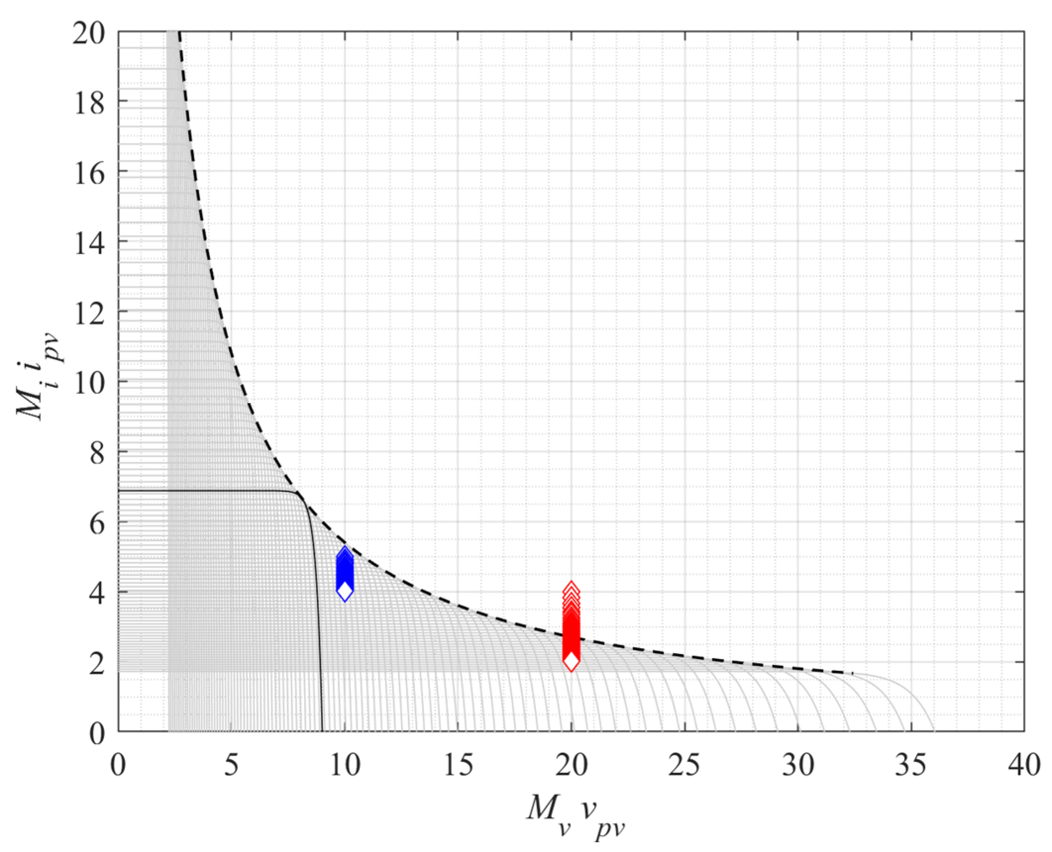
Figure 1. Single diode model for a PV device.
Energies 16 05864 g001
Figure 2. Lossless model for a step-up-down synchronous converter with Zeta topology.
Energies 16 05864 g002
Figure 3. Two possible steady-state models for a lossy DC–DC converter, with imposed voltage at the primary side (a) and at the secondary side (b).
Energies 16 05864 g003
Figure 4. Three possible representations of a SC: (a) ideal; (b) ideal with self-discharge  r s h  resistor; (c) with both self-discharge resistance and series-current limitation.
Energies 16 05864 g004
Figure 6. All possible I–V characteristics of the PV device seen from the SC side, for various duty-cycles. The full line is the PV characteristic, and the dashed line is the envelope of the maximum power points. Blue circle and ×, and red circle and × represent points from Table 1.
Energies 16 05864 g006
Figure 7. Effects of the efficiency, in terms of I–V PV characteristics seen from the SC side, on both voltage and current (a), only current (b) and only voltage (c). Blue circle and ×, and red circle and × represent points from Table 1.
Energies 16 05864 g007
Figure 8. Effect of the shunt resistance in the SDSC case. Larger effects are seen at higher  v M A X .
Energies 16 05864 g008
Figure 9. Absolute value of the time derivative of the SC voltage in logarithmic form (a), showing three regions separated by two curves where the function reaches zero for the IDSC. The IDSC, SDSC and FSC are shown for a fixed  v M A X = 6   V  in (b), underlining the very little difference between the models at steady state.
Energies 16 05864 g009
Figure 10. Phase portrait (normalized) of (21), showing the stability nature of the equilibrium points defined by the yellow curves.
Energies 16 05864 g010
Figure 11. LTSpice schematic for the validation of the IDSC, SDSC and FSC chains.
Energies 16 05864 g011
Figure 12. Time-domain voltage of the SC (left) and stability regions (right) according to (21). If the SC initial voltage is within the stable region, it charges towards the stable equilibrium voltage; otherwise, it discharges to zero.
Energies 16 05864 g012
Figure 13. Load power time-domain profile (top) and SC voltage (bottom) for a short load perturbation.
Energies 16 05864 g013
Figure 14. Load power time-domain profile (top) and SC voltage (bottom) for a long load perturbation.
Energies 16 05864 g014
Figure 15. Dynamic LTSpice model of the FSC chain (top) and comparison (bottom) of the capacitor voltage curve in the dynamic case (blue) and adynamic case (red).
Energies 16 05864 g015
Table 1. Load and supercapacitor combinations to determine the existence of a feasible equilibrium condition.
Symbol   p l o a d   v M A X
Red Cross60 W10 V
Red Circle60 W20 V
Blue Cross40 W10 V
Blue Circle40 W20 V
Disclaimer/Publisher’s Note: The statements, opinions and data contained in all publications are solely those of the individual author(s) and contributor(s) and not of MDPI and/or the editor(s). MDPI and/or the editor(s) disclaim responsibility for any injury to people or property resulting from any ideas, methods, instructions or products referred to in the content.

