Article

Implicit Mathematical Model of Photovoltaic Arrays with Improved Calculation Speed Based on Inflection Points of the Current–Voltage Curves

by
Juan David Bastidas-Rodriguez
1,*,†,
Carlos Andres Ramos-Paja
2,† and
Andres Julian Saavedra-Montes
2,†
1
Facultad de Ingeniería y Arquitectura, Universidad Nacional de Colombia, Manizales 170003, Colombia
2
Facultad de Minas, Universidad Nacional de Colombia, Medellin 050041, Colombia
*
Author to whom correspondence should be addressed.
These authors contributed equally to this work.
Energies 2023, 16(13), 4875; https://doi.org/10.3390/en16134875
Submission received: 21 April 2023 / Revised: 14 June 2023 / Accepted: 19 June 2023 / Published: 22 June 2023
(This article belongs to the Special Issue Advances on Solar Energy and Photovoltaic Devices)

Abstract

:
Dynamic reconfiguration, the monitoring of power production, and the fault diagnosis of photovoltaic arrays, among other applications, require fast and accurate models of photovoltaic arrays. In the literature, some models use the Lambert-W function to represent each module of the array, which increases the calculation time. Other models that use implicit equations to avoid the Lambert-W function do not use the inflection voltages to simplify the system of nonlinear equations that represent the array, increasing the computational burden. Therefore, this paper proposes mathematical models for series-parallel (SP) and total-cross-tied (TCT) photovoltaic arrays based on the implicit equations of the single-diode model and the inflection points of the current–voltage curves. These models decrease the calculation time by reducing the complexity of the nonlinear equation systems that represent each string of SP arrays and the whole TCT. Consequently, the calculation process that solves the model speeds up in comparison with processes that solve traditional explicit models based on the Lambert-W function. The results of several simulation scenarios using the proposed SP model with different array sizes show a reduction in the computation time by 82.97 % in contrast with the traditional solution. Additionally, when the proposed TCT model for arrays larger than 2 × 2 is used, the reduction in the computation time is between 47.71 % and 92.28 % . In dynamic reconfiguration, the results demonstrate that the proposed SP model provides the same optimal configuration but 7 times faster than traditional solutions, and the TCT model is solved at least 4 times faster than classical solutions.

1. Introduction

Photovoltaic (PV) generators have been established as one of the main renewable energy sources adopted to contribute to the decarbonization of electric energy generation around the world. That is why the International Energy Agency estimates that 240 GW of PV systems were installed in 2022 to reach a global capacity of 1185 GW. Although such an installed capacity is saving around 1399 million tons of CO 2 eq, it is expected that PV generators continue growing to reach the goals proposed in COP21 [1].
Because of the increase in PV generators used in electrical systems, the number of applications that use this source is continually increasing. Water pumping systems [2], hybrid generator systems composed of PV arrays, wind generators, batteries [3,4], and PV generators connected to electric grids [5] are very popular. Each application has requirements in control, management, and modeling to operate safely and efficiently. To improve the efficiency of PV generators, maximum power point trackers are developed and applied to the PV arrays [6], and their safe operation is guaranteed using optimized control systems [7]. To analyze the high number of applications of PV generators, several models with several levels of representation are required. The next step is to analyze the multiple connections of PV arrays and the strategies to model them.
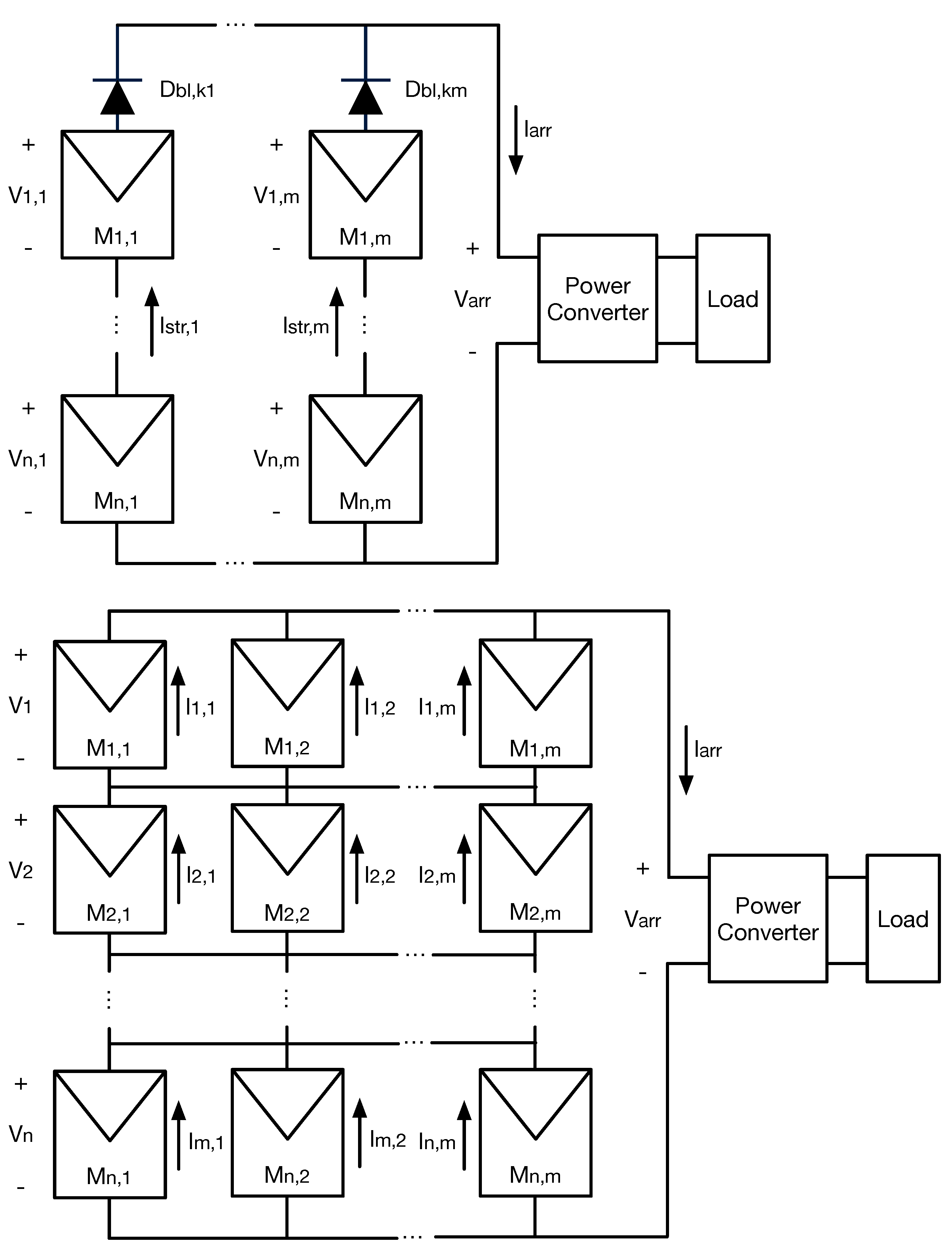
PV arrays can be connected in series-parallel (SP), total-cross tied (TCT), or other configurations. SP is the typical connection used in commercial arrays, and TCT may mitigate the power reduction produced by mismatching conditions (e.g., partial shading) [8,9]. In SP arrays, the number of modules in each string (n) depends on the input voltage required by the PV inverter (or dc/dc converter), while the number of strings connected in parallel (m) is defined according to the power required from the array and considering the power limitations of the inverter (or load). In addition, in SP arrays each string has a diode connected in series, named the blocking diode, to avoid the reverse current through the modules in the string [10]. On the other hand, an n × m TCT array corresponds to n rows connected in series, where each row is formed by m modules connected in parallel. This configuration does not require blocking diodes and, in some cases, mitigates the power reduction produced by non-uniform conditions, which means that not all of the PV modules operate at the same irradiance and temperature and that not all of the PV modules have the same electrical characteristics. However, one disadvantage of TCT arrays is that they require additional wiring [11].
SP and TCT arrays can be modeled as an equivalent circuit generated by the interconnection of the equivalent circuits that represent each module. When an array is operating under non-uniform conditions, it is necessary to solve the equivalent circuit that represents the array’s electrical behavior, which depends on the model adopted to represent each module [10].
The single-diode model (SDM) is the most widely used model of PV modules and provides a satisfactory compromise between accuracy and complexity [10]. In this model, the relation between the module’s voltage (V) and current (I) is given by an implicit equation. Therefore, some models proposed in the literature use the Lambert-W function to obtain I as an explicit function of V [12], while others use the implicit equation [13]. Therefore, the mathematical models of SP and TCT arrays are divided into two main groups: explicit and implicit. Nonetheless, several published works do not use mathematical models of the PV arrays; instead, they solve the PV array equivalent circuit in a circuit simulator [14]. Although the use of circuit simulators to model PV arrays facilitates the modeling of arrays in different configurations, it is not practical when it is required to continuously modify the model parameters, the partial shading conditions, or the array dimensions, which are needed to perform energy production analysis or implement the reconfiguration of controllers.
The objective of the mathematical model of an n × m SP array is to determine the voltages of all of the modules, the string currents, and the array current ( I a r r ), which correspond to the sum of all of the strings currents. To reach that objective, each string can be analyzed independently for a given array voltage ( V a r r ) that is defined by the PV inverter. The explicit models proposed in [12,15,16] use the SDM to represent each module and define a system of nonlinear equations F e for each string, where the n + 1 unknowns correspond to the voltages of the n modules and the blocking diode. In [12], the authors introduce the Jacobian matrix (J) related to the system of nonlinear equations and use F e and J to calculate the unknowns by applying an iterative solution method in Matlab. Later, the authors of [15] proposed a method to calculate the inverse of J symbolically, which speeds up the solution of F e using the Newton–Rapson method. Moreover, that paper also proposes a procedure to determine the guess solution to facilitate the convergence of the Newton–Rapson algorithm. Additionally, the authors of [17] evaluated both deterministic and metaheuristic optimization algorithms to solve F e , concluding that the deterministic ones provided the best results for this problem.
In [16], the authors propose a different explicit approach to model each string of an SP array. The unknown variable is the string current, and the voltage of each module is expressed in terms of the module current by using the Lambert-W function, while the bypass diodes are modeled with the piecewise linear model. Moreover, that paper proposes a method to calculate the inflection voltages in the current vs. voltage (I-V) curve to identify when a module is active or inactive due to the action of the bypass diode, thus simplifying the model of inactive modules to reduce the complexity of the nonlinear equation of the string.
The other mathematical models of the n × m SP arrays consider the SDM without series and parallel resistors (i.e., ideal SDM) to reduce the complexity of the system of nonlinear equations, and, as consequence, the computational burden and calculation time are reduced. An interesting model of this type is the one introduced in [18], where the authors represent each bypass diode as an ideal diode, using the inflection voltages of the I-V curve to reduce the complexity of the system of nonlinear equations that represent each string.
The implicit mathematical model of an n × m SP array, introduced in [13], uses the implicit equation that describes the I-V relationship in the SDM. Then, the model defines a system of n + 2 nonlinear equations ( F i ) and the same number of unknowns for each string, which correspond to the string current and the voltages of the n modules and blocking diode. This model avoids the evaluation of the Lambert-W function, which reduces the computational burden of the iterative solution method of F i and, as consequence, reduces the calculation time required to solve F i regarding the explicit models with SDM. Furthermore, in [19] the authors evaluated deterministic and metaheuristic optimization algorithms to solve F i and found that deterministic options show better performance in different cases.
Regarding the models of an n × m TCT array, the objective is to determine the currents of all of the modules; the voltages of the rows; and the array current, which corresponds to the sum of the modules’ current in one row. In the literature, there are some mathematical models for n × m TCT arrays [20,21] and others for arrays with particular dimensions such as 2 × 2  [22,23] or 4 × 4 [24]. In addition, some of those models use the SDM [20,24], the SDM without the parallel resistance [23], or the SDM without series and parallel resistors (i.e., ideal SDM) [20,22]. Moreover, some models focus on particular shading patterns [22,23,24], while others can be applied to any shading condition [20,21].
The models proposed in [20,21] define a system of nonlinear equations that represent the TCT, and their main difference is that one model uses the ideal SDM [20], while the other one uses the SDM. Additionally, in [20] the authors propose a method to calculate the inflection points in the I-V curve when a row is active or inactive, which enables one to neglect such a row in the analysis, thus simplifying the system of nonlinear equations. Instead, in [21] the authors propose a procedure to explicitly determine the inverse of the Jacobian matrix associated with the system of nonlinear equations that describe the array; hence, the solution of the system of nonlinear equations can be sped-up with iterative methods such as the Newton–Raphson.
In the models previously described, there are two strategies to reduce the calculation time of the models that use the SDM to represent each module. The first one is the use of the inflection voltages of the I-V curves to identify the active bypass diodes (i.e., inactive modules in SP arrays and inactive rows in TCT arrays); then, the inactive modules or rows can be represented with simplified models that reduce the complexity of the system of nonlinear equations describing the arrays. The other strategy is to use the implicit equation of the SDM to avoid the evaluation of the Lambert-W function, which reduces the computational burden required to solve the system of nonlinear equations. However, the models that use the inflection voltages use the Lambert-W function to represent each module of the array, which increases the calculation time, while the models that use implicit equations to avoid using Lambert-W function do not use the inflection voltages to simplify the system of nonlinear and implicit equations that represent the array, which augments the computational burden. Those increments in the calculation times restrict the application of those models in applications where this indicator is critical, such as reconfiguration systems.
The objective of this paper is to propose mathematical models for SP and TCT PV arrays based on the implicit equations of the SDM and the inflection points of the current–voltage curves. These models reduce the calculation time by reducing the complexity of the nonlinear equation systems that represent each string of SP arrays and the whole TCT array. Specifically, two approaches are used to reduce the complexity of the implicit models of SP and TCT PV arrays; the first approach is the simplification of the system of nonlinear and implicit equations, which is based on the fact that the modules or rows, for TCT, with active bypass diodes can be represented by a current source in parallel with the bypass diode, which can be represented by explicit equations. The second strategy is the definition of restricted search spaces for the solution of the simplified system of nonlinear and implicit equations. This is achieved by using the voltages and currents for each IP, which define a specific search range for each unknown voltage or current, thus reducing the solution time of the numerical method that solves the system of equations. Consequently, the calculation process that solves the model significantly speeds up in comparison with processes that solve traditional explicit models based on the Lambert-W function. For example, in several simulation scenarios with multiple array sizes, the proposed SP model is faster than the traditional solution, reducing the computation time by 82.97 % . On the other hand, the proposed TCT model provides a reduction time between 47.71 % and 92.28 % for arrays larger than 2 × 2 . For dynamic reconfiguration purposes, where both SP and TCT arrays were partially reconfigured to improve power production under two partial-shading conditions, the results demonstrate that the proposed solution provides the same optimal configuration but more than 7 times faster for SP reconfigurations, and between 4 and 6 times faster for TCT reconfigurations.
The rest of the paper is organized as follows: Section 2 explains the structure of SP; the TCT arrays; the SDM equations; and the parameters, as well as their dependence on the irradiance and temperature. Then, Section 3 introduces the proposed procedure to determine the inflection voltages and currents by using the implicit equations for both the SP and TCT arrays. Later, Section 4 introduces the proposed implicit models of SP and TCT arrays and describes the use of inflection voltages and currents to reduce the complexity of the system of nonlinear equations that represents the arrays; also, the section presents a comprehensive flowchart describing the complete model processing. Subsequently, Section 5 demonstrates the validity and accuracy of the proposed models for arrays with different dimensions through simulation and experimental results. This section includes two practical applications for dynamic reconfiguration purposes, which illustrate the practical advantage of the reduction in the calculation time obtained with the proposed model. Finally, the conclusions close the paper.

2. SP and TCT Arrays

The general structure of n × m PV arrays in SP and TCT configurations is illustrated in Figure 1. On the one hand, SP arrays are formed by m strings (or columns) connected in parallel, where each string is formed by n PV modules (black rectangles) and one blocking diode ( D b l k ) connected in series. On the other hand, TCT arrays are formed by n rows connected in series, and each row has m PV modules connected in parallel. In both configurations, n depends on the minimum and maximum input voltage of the power converter, while m is defined according to the maximum power required by the load and supported by the power converter. In a PV system, the power converter modifies the array voltage ( V a r r ), and, as consequence, the PV array delivers a particular current ( I a r r ), which depends on the irradiance and temperature of the modules as well as the modules’ parameters. Therefore, the main objective of a PV array model is to determine I a r r for a given value of V a r r . However, it is necessary to determine other arrays’ variables (voltages and currents) before calculating I a r r ; thus, the following subsections describe the implicit model used to describe the electrical behavior of a PV module and a blocking diode (Section 2.1), and the PV array’s parameters and variables (Section 2.2).

2.1. Models of PV Modules and Blocking Diodes

The single-diode model (see Figure 2) is one of the most widely used representations to reproduce the electrical behavior of PV modules, which is considered as a set of N s series-connected cells with a bypass diode (BD) connected in antiparallel. The single-diode model is formed by an independent current source ( I p h ) that describes the photovoltaic effect, a diode (D) that describes the nonlinear behavior of the N s PV cells, a resistor in parallel ( R h ) to include the leakage currents, and a resistor in series ( R s ) to consider the ohmic losses. Applying Kirchhoff’s current law (KCL), it is possible to obtain the implicit expression of the module’s current (I) and voltage (V) shown in Equation (1) [13], where I s , η , and V t are the inverse saturation current, ideality factor, and thermal voltage of diode D, respectively, while I b d is the bypass diode’s current, which is defined in the explicit equation Equation (2). In this last expression, I s b d , η b d , and V t b d represent the inverse saturation current, ideality factor, and thermal voltage of the bypass diode BD, respectively. The thermal voltages of D and BD are defined as V t = k · T / q and V t b d = k · T b d / q , respectively, where k is the Boltzmann constant, q is the electron charge, T is the cells’ temperature, and T b d is the BD temperature. In this paper, it is assumed that T b d T [25] since both D and BD are part of the same mechanical structure since in most of the PV modules, the bypass diodes are installed in a junction box located at the back of the PV panel. In such a junction box, the connections of the modules are inside the PV panel and the bypass diodes and the two cables of the PV panel come out from this box.
f V , I = I + I p h I s · exp V + I I b d · R s N s · η · V t 1 V + I I b d R h + I b d
I b d ( V ) = I s b d · exp V η b d · V t b d 1
In addition, in this paper it is considered that the SDM model parameters depend on the irradiance (G) and temperature (T), as shown in Equations (3)–(8). The expressions (3), (6), and (8) were taken from [26], while expressions (4) and (5) were obtained from [27] and [28], respectively. In those expressions, the subindex s t c is used to indicate the parameter or variable under standard test conditions (STC), which are calculated from the datasheet parameters or experimental measurements by following the procedure proposed in [29]. Moreover, in Equations (4) and (7), the parameters α I s c and α V o c are the temperature coefficients of the short-circuit current ( I s c ) and open-circuit voltage ( V o c ), respectively. Finally, the bypass diode’s parameters I s b d and η b d can be calculated from the datasheet information, i.e., the reverse current and one operating point at a known temperature.
η ( T ) = η s t c · ( T / T s t c )
I s ( T ) = I s , s t c + α I s c · ( T T s t c ) exp V o c , s t c + α V o c · ( T T s t c ) N s · η · V t 1
R s ( T , G ) = R s , s t c + T T s t c · 1 0.217 · ln G G s t c
R h ( G ) = R h , s t c · G G s t c
I s c = G G s t c · I s c , s t c + α I s c · ( T T s t c )
I p h ( T , G ) = I s c + I s · exp I s c · R s N s · η · V t 1 + I s c · R s R h
In SP arrays, there are m blocking diodes (one per string), and they are also represented with the exponential model, as introduced in Equation (9), where I s t r and V b k are the diode’s current and voltage, respectively (as defined in Figure 1), and I s b k and η b k correspond to the inverse saturation current and ideality factor, respectively. Moreover, the thermal voltage is defined as V t b k = k · T b k / q , with T b k representing the blocking diode’s temperature.
I s t r ( V b k ) = I s b k · exp V b k η b k · V t b k 1

2.2. Array’s Parameters and Variables

For an n × m SP or TCT array, the SDM parameters of the PV modules can be defined by adding the subindexes i and j to the parameters defined in Section 2.1, where subindex i represents the row and subindex j represents the column; hence, i [ 1 , , n ] and j [ 1 , , m ] . Keeping this in mind, the SDM parameters are: I s c , i , j , I p h , i , j , I s , i , j , η i , j , V t , i , j , R s , i , j , R h , i , j , I s b d , i , j , η b d , i , j , and V t b d , i , j . Further, the blocking diodes’ parameters can be defined using only subindex j since there is only one per string in the SP arrays ( I s b k , j , η b k , j , and V t b k , j ). Therefore, subscripts i and j indicate that the SDM parameters of each PV module and the parameters of each blocking diode can be different.
Moreover, the model also considers that each PV module can experience different operating conditions (irradiance and temperature); therefore, subindexes i and j are also used to define the irradiance and temperature of each module, i.e., G i , j and T i , j represent the irradiance and temperature of a module in row i and column j of the array, respectively.
Additionally, the array’s variables are defined with one scalar for the array current ( I a r r ) and a set of voltages and currents of the PV modules. For SP arrays, the string current is defined as the current of the first module ( I 1 , j j [ 1 , , m ] ) and the modules’ voltages are defined using subindexes i and j ( V i , j ) as explained before. In TCT arrays, the row voltages are defined as the voltage of the first module in the row ( V i , 1 i [ 1 , , n ] ) and the module currents are defined using subindexes i and j ( I i , j ).

2.3. Characteristic Curves of a PV System

The electrical behavior of PV systems is reported using the current vs. voltage (I-V) and power vs. voltage (P-V) curves, which depend on both the irradiance and temperature. The I-V curve of a PV system is obtained from experiments where the PV voltage is changed from 0 V to V o c while the PV current is measured and registered. This same process (voltage sweep) can be applied to the SDM model to obtain the predicted I-V curve of a module, string, or array. The P-V curves are generated by multiplying the PV current and voltage, and despite its simplicity, this curve is required to evaluate the produced power and the optimal operating voltage and current of a PV system.
For example, Figure 3 shows an SP array formed by four ERDM-85 [30] PV modules, where two modules are fully irradiated ( M 2 , 1 and M 1 , 2 ), while the other two modules have a different shaded area ( M 1 , 1 and M 2 , 2 ). Those irradiance and shading conditions produce short-circuit currents I S C 2 , 1 = I S C 1 , 2 = 5.15 A for M 2 , 1 and M 1 , 2 ; I S C 1 , 1 = 4.5 A ( 12.6 % shading) and I S C 2 , 2 = 1.0 A (80.6 % shading). The figure shows the I-V curves of the four modules, where the different electrical profiles are observed. However, in Section 2.1 it is described that the PV modules have bypass diodes, which are activated when the current applied to the module is higher than the short-circuit current. The effect of the bypass diode activation is observed in the I-V curves of the strings, which is also observed in Figure 3: the activation of the bypass diodes avoids the operation of the modules with negative voltages (consuming power), but this introduces a discontinuity in the I-V curve, which is known as inflection points (IP); the figure shows the IP produced in both strings due to activation of the bypass diodes associated with M 1 , 1 (String 1) and M 2 , 2 (String 2).
The I-V curve of the array is also presented in Figure 3, where the array current I a r r is the sum of the string currents I s t r , 1 and I s t r , 2 produced by the same string voltage V a r r , which is the same array voltage. Such an I-V curve of the array shows two IPs, which are produced by the IP of each string. In addition, the P-V curve of the array is also presented, where the two IPs are also observed. Finally, the P-V curve shows the existence of two maximum power points (MPP); the one with the highest power is commonly named the global maximum power point (GMPP), and any other MPP is known as a local maximum power point (LMPP). Therefore, the PV array (or string) must always be operated at the GMPP to maximize the power production of the PV system, and the optimal array voltage (and current) can be easily predicted by using the P-V curve of the array.

3. Calculation of Inflection Points (IPs) Using Implicit Equations

The inflection points (IPs) in the current vs. voltage (I-V) curve of an array, independently of its configuration [31], are produced by the activation/deactivation of the bypass diodes in the PV modules. In general, a bypass diode is active while the current flowing through a given module ( I i , j ) is higher than its short-circuit current ( I s c , i , j ), i.e., I i , j > I s c , i , j ; otherwise, when I i , j < I s c , i , j the bypass diode is inactive because it is reverse-biased.
The solution of the system of nonlinear equations that represents the array may be complicated close to the IPs; this is due to the large variations in the current derivatives with respect to the voltage. However, points can be used to reduce the complexity of the system of nonlinear and implicit equations that describe the arrays and, as consequence, to reduce the model solution time. Therefore, the following subsections describe the proposed procedures to calculate the inflection voltages in implicit models of SP and TCT arrays. Those points are used in Section 4 to reduce the complexity of the models and improve their calculation speed.

3.1. IPs Calculation in SP Arrays

In an SP array, each string can be analyzed independently due to its parallel connection to the input of the power converter; hence, this section shows the calculation procedure of the IPs in a single string (j-th string) and how to organize the information obtained. Then, the same procedure can be repeated for each string to obtain the IPs of the entire array.
The first step to calculate the IPs of string j is to sort the modules in descending order according to their short-circuit currents, i.e., I s c , k , j > I s c , k + 1 , j with k [ 1 n ] . Then, the number of IPs in a string is n since there is one IP when the current of string j ( I 1 , j ) is equal to the short-circuit current of a module, i.e., I 1 , j = I s c , k , j with k [ 1 n ] .
To calculate the k-th IP, it is important to mention that the string current ( I 1 , j = I s c , k , j ) and the k-th module voltage ( V k , j = 0 V ) are known; hence, there are n unknowns that correspond to the array voltage ( V a r r ) and the voltages of the n 1 PV modules ( V k , j with k [ 1 , , k 1 , k + 1 , , n ] ). The voltage of the blocking diode ( V n + 1 , j ) can be expressed as a function of the string current as shown in Equation (10); therefore, it is not considered an unknown.
V n + 1 , j ( I 1 , j ) = η b k , j · V t b k , j · ln I 1 , j I s b k , j + 1
The system of nonlinear and implicit equations that describes the electrical behavior of string j at k-th IP is introduced in Equation (11), where the first n 1 equations correspond to the implicit equations of the PV modules in the string (except module k), while the last equation is obtained by applying the Kirchhoff voltage law (KVL) to the string considering the definition of V n + 1 , j given in Equation (10). In expression (11), V m , k , j is an ( n 1 ) × 1 vector with the modules voltages (except V k , j ), and V a , k , j is the array voltage for the k-th IP.
F S P 1 ( V m , k , j , V a , k , j ) = f ( V 1 , j , I 1 , j ) = 0 f ( V k 1 , j , I 1 , j ) = 0 f ( V k + 1 , j , I 1 , j ) = 0 f ( V n , j , I 1 , j ) = 0 Σ i = 1 k 1 V i , j + Σ i = k + 1 n V i , j + V n + 1 , j ( I 1 , j ) V a , k , j = 0
The previous system of nonlinear equations can be solved as an optimization problem or with the solvers provided by different software (e.g., fsolve in Matlab) to obtain the n modules voltages for k-th IP of the string j, which are organized in an n × 1 vector named V m I P , k , j as shown in Equation (12).
V m I P , k , j = V m , k , j ( 1 ) , , V m , k , j ( k 1 ) , 0 , V m , k , j ( k + 1 ) , , V m , k , j ( n 1 ) T
Then, solving expression (11) for the n modules of the string j enables one to construct an n × 1 vector ( V a I P , j ) with the array voltages as shown in Equation (13). Such a V a I P , j vector is used in Section 4.1 for the proposed modeling procedure of SP arrays.
V a I P , j = V a , 1 , j , , V a , n , j T
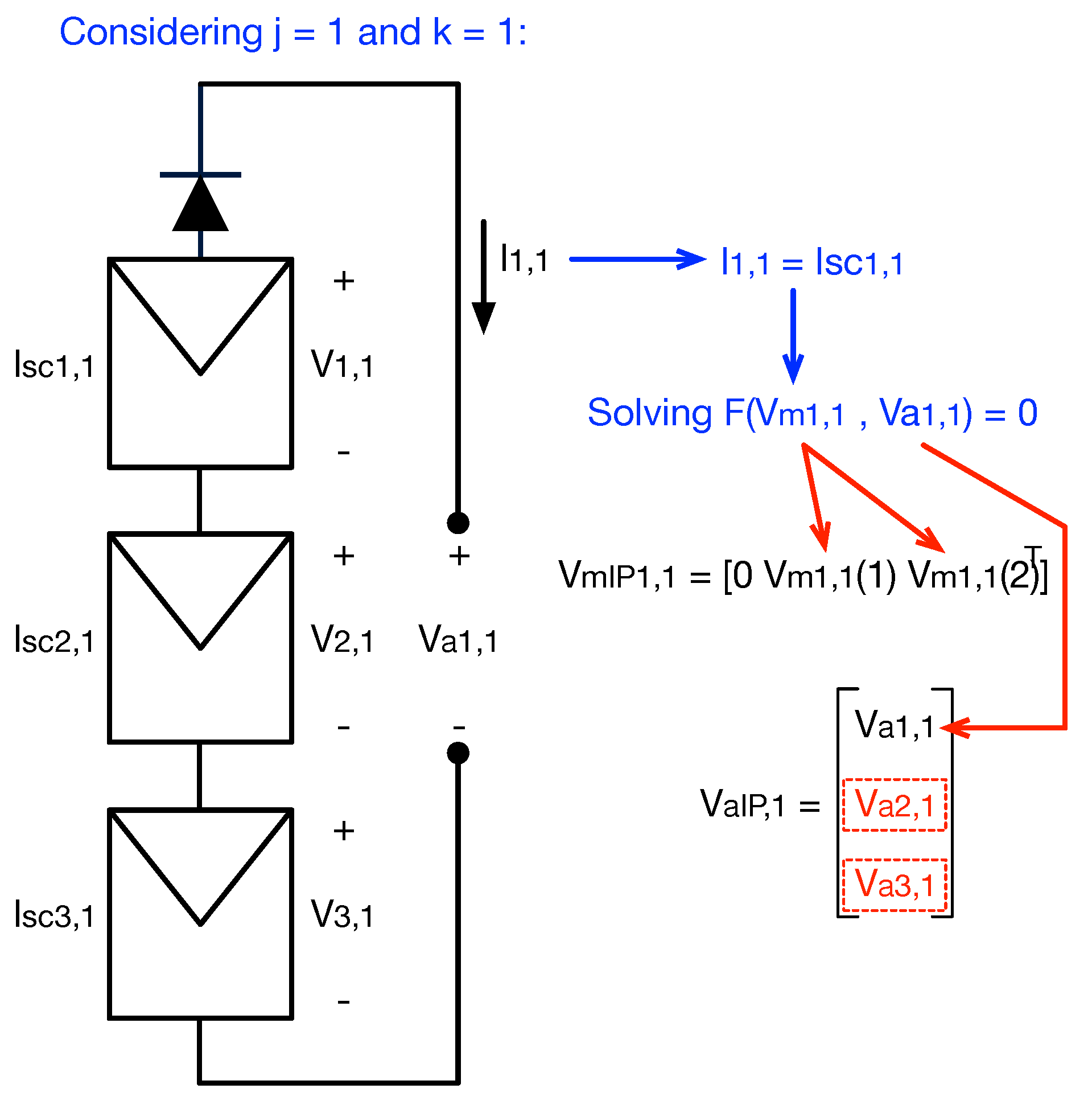
Figure 4 illustrates the generation of V m I P , k , j and V a I P , j for an SP array with one string ( j = 1 ) and three modules ( n = 3 ), where I s c , 1 , 1 I s c , 2 , 1 I s c , 3 , 1 . Considering the string current is equal to the short-circuit current of the first module ( I 1 , 1 = I s c , 1 , 1 ), V m , 1 , 1 and V a , 1 , 1 are obtained by solving expression (11). Then, V m I P , 1 , 1 is generated from V m , 1 , 1 , and V a , 1 , 1 is the first element of V a I P , 1 . Finally, V m I P , 2 , V m I P , 2 , and V a I P , 1 can be completed by repeating this process for I 1 , 1 = I s c , 2 , 1 and I 1 , 1 = I s c , 3 , 1 . In this example, if T b k T = 45 C = 318.15 K , the model parameters are I p h = 5.1544 A , η = 1.1324 , I s = 0.7497 η A , R s = 0.1989 Ω , R h = 261.0999 Ω , I s , b d = I s , b k = 1 μ A , and η b d = η b k = 0.2694 , and the short-circuit currents are I s c , 1 , 1 = 5.15 A , I s c , 2 , 1 = 3.60 A , and I s c , 3 , 1 = 2.06 A ; then, V m 1 , 1 = [ 0.098 0.1034 ] V , V m I P 1 , 1 = [ 0 0.098 0.1034 ] V , and V a 1 , 1 = 0.309 V .

3.2. IPs Calculation in TCT Arrays

An n × m TCT array can be analyzed as n rows connected in series, where each row is formed by m PV modules connected in parallel. Keeping this in mind, the calculation of IPs for TCT arrays is similar to the one of a string in an SP array, i.e., the k-th IP is generated when the array current ( I a r r ) is equal to the sum of the short-circuit currents of the row k ( I r s c , k ). Therefore, in a TCT array, there will be n IPs, and this section shows the procedure to calculate them.
The first step is to sort the rows in descending order according to the sum of the short-circuit currents of each row I r s c , k , which is defined in Equation (14). Hence, after this step, the condition I r s c , k > I r s c , k + 1 with k [ 1 , , n ] is fulfilled.
I r s c , k = j = 1 m I s c , k , j k [ 1 , , n ]
For the calculation of the k-th IP, the array current and the k-th row voltage are defined as I a r r = I r s c , k and V k , 1 = 0 V , respectively. Therefore, there are ( n 1 ) · m + n unknowns to solve, which correspond to the array voltage ( V a , k ), n 1 rows voltages ( V r , k ) excluding V k , 1 , and ( n 1 ) · m module currents excluding the ones of row k ( I m , k ).
The system of nonlinear and implicit equations that describe the electrical behavior of a TCT array is introduced in expression (15), where the first ( n 1 ) · m expressions correspond to the implicit equations of the modules in all of the rows, except row k; the next n 1 equations are obtained by applying the KCL to the n 1 nodes between two consecutive rows; and the last equation results from the application of KVL with the array voltage and rows voltages, excluding row k. In the KCL equations of expression (15), it is important to remark that the sum of the currents in row k corresponds to I r s c , k ; hence, m j = 1 I k , j = I r s c , k .
F T C T 1 ( V r , k , V a , k , I m , k ) = f ( V 1 , 1 , I 1 , 1 ) = 0 f ( V k 1 , 1 , I k 1 , m ) = 0 f ( V k + 1 , 1 , I 1 , 1 ) = 0 f ( V n , 1 , I n , m ) = 0 ( n 1 ) · m implicit equations Σ j = 1 m I 1 , j Σ j = 1 m I 2 , j = 0 Σ j = 1 m I n 1 , j Σ j = 1 m I n , j = 0 ( n 1 ) KCL Σ i = 1 k 1 V i , 1 + Σ i = k + 1 n V i , 1 V a , k = 0 1 KVL
The solution of F T C T 1 ( V r , k , V a , k , I m , k ) can be obtained by using optimization algorithms or the nonlinear-equations solvers provided in different software, where the results are as follows: the array voltage ( V a , k ), an ( n 1 ) × 1 vector with the rows’ voltages ( V r , k ), and an ( n 1 ) · m × 1 vector with the modules’ currents ( I m , k ). In this last vector, the currents are organized as shown in Equation (16), i.e., the module currents in column 1 followed by the ones in column 2, and so on, to complete the module currents of the m columns. Those results correspond to the k-th IP, or the IP produced by the k-th row, which must be organized to be used in the model solution as explained in Section 4.2.
I m , k = I i , 1 , I i , 2 , , I i , m T i [ 1 , k 1 , k + 1 , , n ]
The array voltages for the n IPs are organized into an n × 1 vector named V a I P , which is defined in Equation (17). Additionally, the rows’ voltages are organized in an n × 1 vector named V m I P , k , as shown in Equation (18), to include the k-th row voltage ( 0 V ).
V a I P = V a , 1 , , V a , n T
V m I P , k = V r , k ( 1 ) , , V r , k ( k 1 ) , 0 , V r , k ( k + 1 ) , , V r , k ( n 1 ) T
Moreover, the modules’ currents are organized into an n × m matrix ( M i m I P , k ) that includes the currents of all of the modules, as shown in Equation (19). In such a matrix, the currents of the modules in row k are defined by their short-circuit currents, while the currents of the other rows correspond to the elements of the vector I m , k . It is worth noting that M i m I P , k corresponds to the k-th IP; therefore, there is one matrix for each IP.
M i m I P , k = I m I P ( i , j ) , where , I m I P ( k , j ) = I s c , k , j j [ 1 , , m ] and , I m I P ( i , j ) = I m , k ( i + ( j 1 ) · ( n 1 ) ) i [ 1 , k 1 , k + 1 , , n ] j [ 1 , , m ]
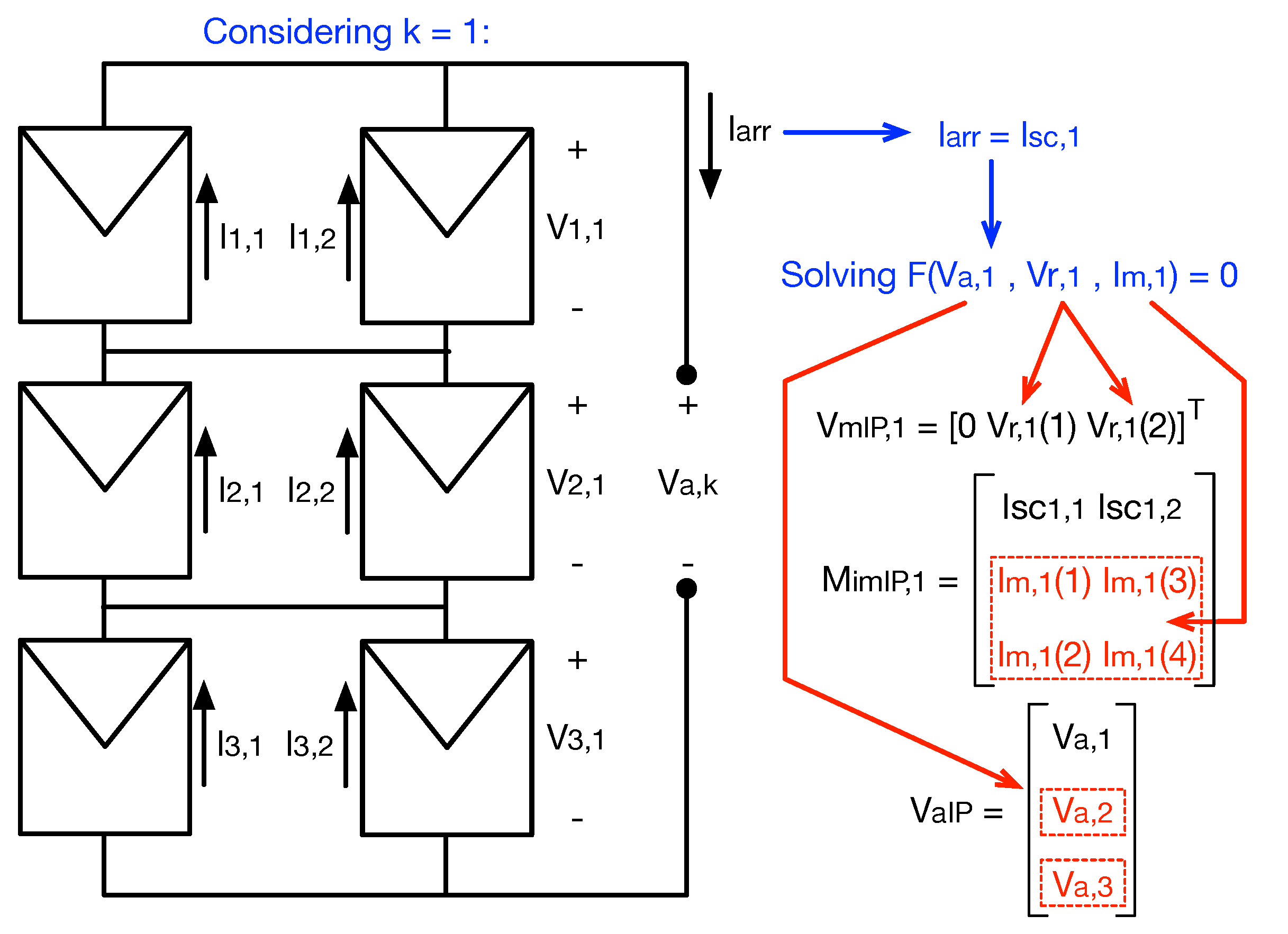
Figure 5 illustrates the generation of V m I P , k and M i m I P , k for a TCT array with two columns ( m = 2 ) and three rows ( n = 3 ), where I r s c , 1 I r s c , 2 I r s c , 3 . Considering I a r r = I r s c , 1 (i.e., k = 1 ), then the array voltage ( V a , 1 ), the rows voltages ( V r , 1 = [ V 1 , 1 , V 2 , 1 , V 3 , 1 ] T ), and the currents in the second and third rows ( I m , 1 = [ I 2 , 1 , I 2 , 2 , I 3 , 1 , I 3 , 2 ] T ) are obtained by solving expression (15). V a , 1 is the first element of V a I P , while V m I P , 1 is generated from V r , 1 , and M i m I P , 1 is constructed from the short-circuit currents of the modules in row 1 and the elements of I m , 1 . In this example, the model parameters are the same ones used in Section 3.1 and the short-circuit currents are I s c , 1 , 1 = 5.1544 A , I s c , 2 , 1 = 3.6081 A , I s c , 3 , 1 = 2.0618 A , I s c , 1 , 2 = 4.12 A , I s c , 2 , 2 = 2.57 A , and I s c , 3 , 2 = 1.03 A ; then, V r , 1 = [ 0.0987 0.1034 ] V , V m I P , 1 = [ 0 0.0987 0.1034 ] V , I m , 1 = [ 5.1541 5.1541 4.1239 4.1239 ] A , V a , 1 = 0.2021 V , and M i m I P , 1 , as shown in Equation (20).
M i m I P , 1 = 5.1544 4.1236 5.1541 4.1239 5.1541 4.1239

4. Models of SP and TCT Arrays Using IPs

The IPs calculated in Section 3 are used to improve the calculation speed of the implicit models of the SP and TCT arrays by means of two strategies. The first one is the simplification of the system of nonlinear and implicit equations that represent each string in the SP arrays, and the complete array in TCT configurations. Such a simplification is based on the fact that the modules or rows (for TCT) with active bypass diodes can be represented by a current source in parallel with the bypass diode, which can be represented by explicit equations.
The second strategy to improve the models’ calculation speed is the definition of restricted search spaces for the solution of the simplified system of nonlinear and implicit equations. This is achieved by using the voltages and currents for each IP calculated in Section 3, which define a specific search range for each unknown voltage or current, thus reducing the solution time of the numerical method that solves the system of equations. The following subsections describe the procedures to model SP and TCT arrays by using IPs to reduce the calculation times.

4.1. Model of SP Arrays Using IPs

As descibed before, an SP array can be analyzed string by string; therefore, this section provides the procedure to model the j-th string by using the IPs calculated in Section 3.1. In this section, the objective is to calculate the string current ( I 1 , j ) and the modules voltages ( V 1 , j , , V n , j ) for a given array voltage ( V a r r ); hence, at this point, there are n + 1 unknowns since the blocking diode voltage can be expressed as a function of I 1 , j , as shown Equation (10).
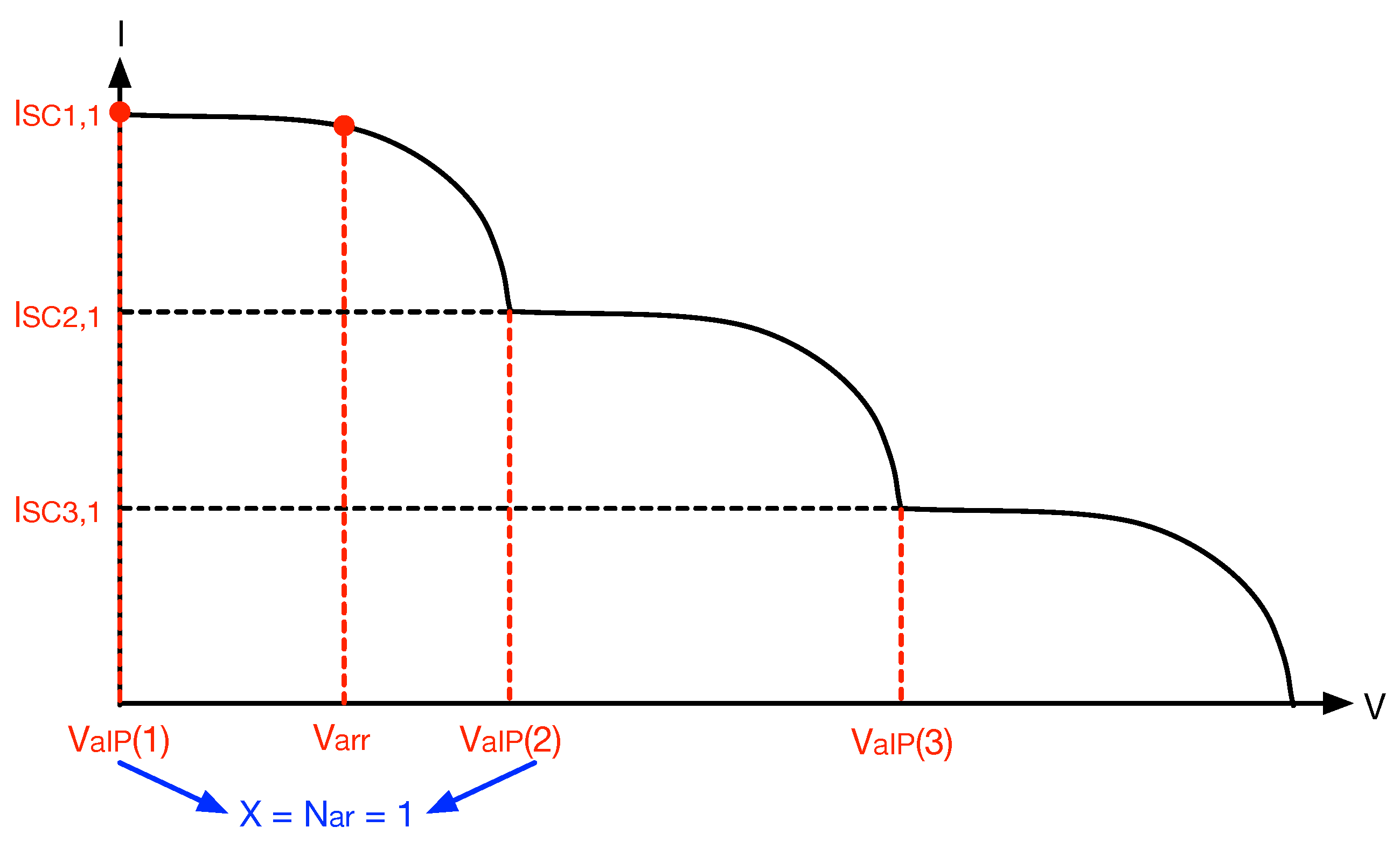
The procedure begins by considering that the modules in the string are organized in descending order according to their short-circuit currents ( I s c , k , j > I s c , k + 1 , j with k [ 1 n ] ). Then, it is necessary to identify the location of V a r r regarding the array voltage IPs in vector V a I P , j , i.e., the value of x such that V a I P , j ( x ) > V a r r > V a I P , j ( x + 1 ) ; this means that PV modules 1 to x are active (or with the bypass diode inactive), and the rest, from x + 1 to n, are inactive (or with the bypass diode active). Therefore, the number of active modules is defined as N a m = x .
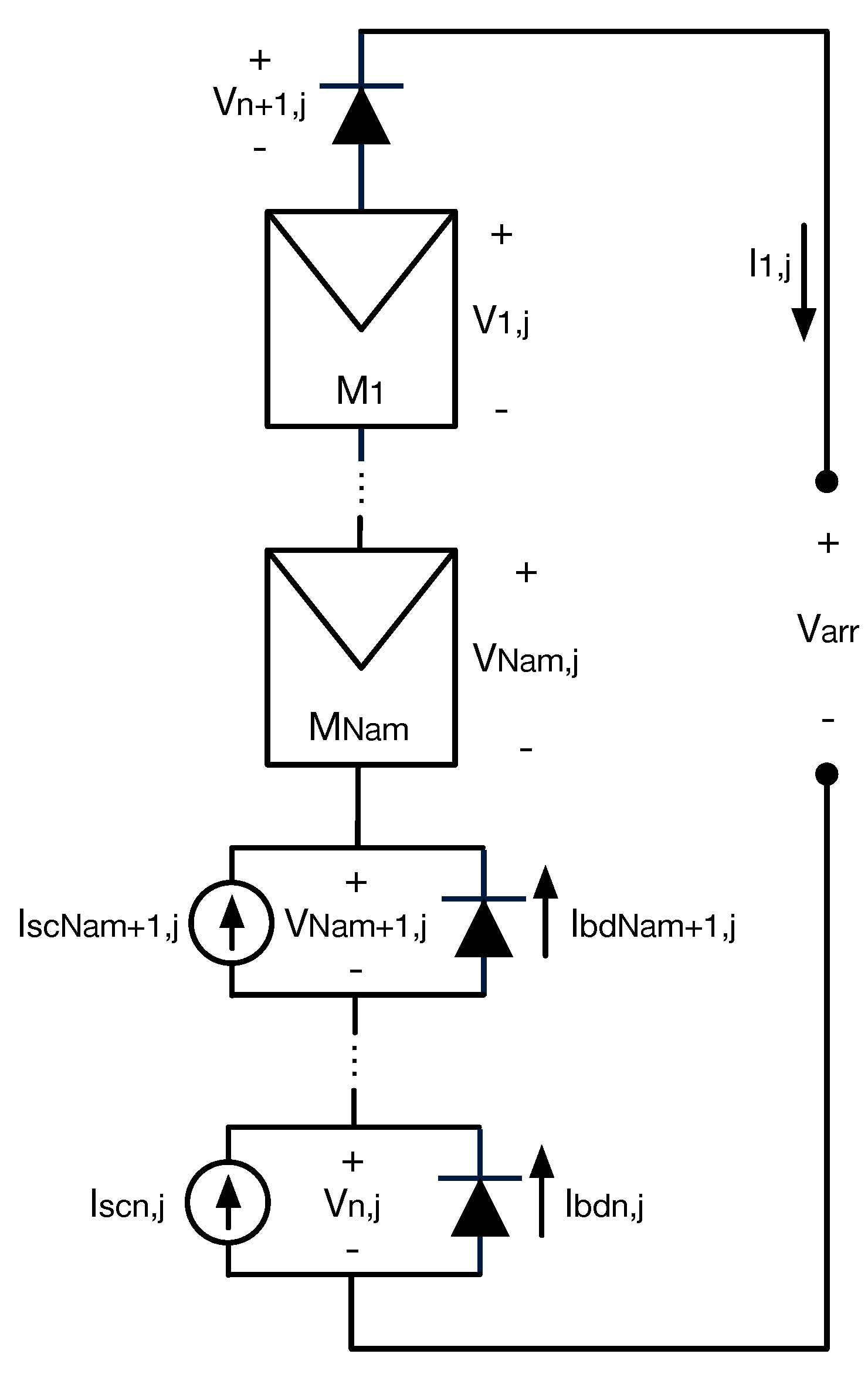
The N a m active modules can be modeled with Equation (1), while the inactive modules can be approximated by a current source with the short-circuit current in parallel with the bypass diode, as shown in Figure 6. Hence, the voltage of the inactive modules can be expressed in terms of the string current as introduced in Equation (21).
V n a , k , j ( I 1 , j ) = η b d , k , j · V t b d , k , j · ln I 1 , j I s c , k , j I s b d , k , j + 1 k [ N a m + 1 , , n ]
The system of implicit and nonlinear equations that describes the j-th string for a given value of V a r r , considering the models of both the active and inactive modules, is presented in expression (22). In this expression, there are N a m + 1 unknowns that correspond to the string current ( I 1 , j ) and the voltages of the active modules, which are organized into a vector V s t r , j = [ V 1 , j , , V N a m , j ] T . The voltages of the inactive modules and the blocking diode are included in the last equation of F S P 2 , which are explicit functions of I 1 , j as shown in Equations (21) and (10), respectively. Therefore, F S P 2 has N a m + 1 equations instead of n, where the first N a m corresponds to the implicit current–voltage relationship of each active module, and the last equation results from applying KVL to the string.
F S P 2 ( V s t r , j , I 1 , j ) = f ( V 1 , j , I 1 , j ) = 0 f ( V N a m , j , I 1 , j ) = 0 Σ i = 1 N a m V i , j + Σ i = N a m + 1 n V n a , i , j ( I 1 , j ) + V n + 1 , j ( I 1 , j ) V a r r = 0
The identification of x, such that V a I P , j ( x ) > V a r r > V a I P , j ( x + 1 ) , is also used to define the upper and lower bounds for the solution of F S P 2 . On the one hand, the solution of I 1 , j is restricted between the short-circuit current of IPs x and x + 1 (i.e., I s c , x , j > I 1 , j > I s c , x + 1 , j ) since the string current is monotonically decreasing in the I-V curve of a string (i.e., d I 1 , j / d V a r r < 0 A / V ). On the other hand, the N a m unknown voltages can be restricted by using the first N a m elements of the vectors V m I P , x , j and V m I P , x + 1 , j . Hence, the search range for V s t r , j and I 1 , j for a given value of V a r r is shown in Equation (23). However, when V a r r is higher than the maximum array IP voltage ( V a r r > V a I P , j ( n ) ), it is not possible to find a value of x such that V a I P , j ( x + 1 ) > V a r r > V a I P , j ( x ) . In those cases, the limits must be defined as shown in Equation (24), where the maximum voltage of the modules is given by their open-circuit voltage in STC and the minimum string current is 0 A .
V m I P , x + 1 , j ( 1 ) > V 1 , j > V m I P , x , j ( 1 ) V m I P , x + 1 , j ( N a m ) > V N a m , j > V m I P , x , j ( N a m ) I s c , x , j > I 1 , j > I s c , x + 1 , j if   x < n
V o c , s t c > V 1 , j > V m I P , n , j ( 1 ) V o c , s t c > V N a m , j > V m I P , n , j ( N a m ) I s c , n , j > I 1 , j > 0 if   V a r r > V a I P , j ( n )
Once F S P 2 ( V s t r , j , I 1 , j ) is solved, the voltages of the inactive modules can be calculated from the string current by using Equation (21). At this point, all of the voltages and currents of the string are known. In conclusion, by applying the proposed procedure it is possible to simplify the model of each string since the system of nonlinear and implicit equations has N a m + 1 equations and unknowns instead of n; moreover, the search range for the solution of F S P 2 ( V s t r , j , I 1 , j ) is defined from the IPs. Those two improvements reduce the calculation time of V s t r , j and I 1 , j for a given V a r r , as will be quantified in Section 5.
Figure 7 shows an example of an I-V curve for the array introduced in Figure 4, which shows the location of an arbitrary value of V a r r regarding the array IPs voltages. In this case, x = N a m = 2 ; therefore, F S P 2 and the solution search range are defined in Equations (25) and (26), respectively. In expression (25), the voltages of the inactive module ( V 3 , 1 ) and the blocking diode ( V 4 , 1 ) are explicit functions of I 1 , 1 according to Equations (21) and (10), respectively.
F S P 2 ( V s t r , 1 , I 1 , 1 ) = f ( V 1 , 1 , I 1 , 1 ) = 0 f ( V 2 , 1 , I 1 , 1 ) = 0 V 1 , 1 + V 2 , 1 + V 3 , 1 ( I 1 , 1 ) + V 4 , 1 ( I 1 , 1 ) V a r r = 0
V m I P , 3 , 1 ( 1 ) > V 1 , 1 > V m I P , 2 , 1 ( 1 ) V m I P , 3 , 1 ( 2 ) > V 2 , 1 > V m I P , 2 , 1 ( 2 ) I s c , 2 , 1 > I 1 , 1 > I s c , 3 , 1

4.2. Model of TCT Arrays Using IPs

Considering an n × m TCT array as n rows connected in series, where each row is formed by m modules connected in parallel, the objective of this section is to propose a procedure to calculate n · m + n unknowns, which correspond to the voltages of the n rows ( V 1 , 1 , , V n , 1 ) and the currents of the n · m modules, for a given value of V a r r . Then, the array current can be calculated as the sum of the currents of any row.
The first step is to sort the arrays in descending order according to the sum of the short-circuit currents in each row, i.e., I r s c , k > I r s c , k + 1 with k [ 1 , , n ] , where I r s c , k is defined in Equation (14). The second step is to determine the location of V a r r regarding the array IPs voltages in V a I P , which is defined in Equation (17), i.e., to determine x such that V a I P ( x ) > V a r r > V a I P ( x + 1 ) . This means that rows from 1 to x are active (no bypass diodes are active) and rows from x + 1 to n are inactive (at least one bypass diode active in the row). Hence, the number of active rows is defined as N a r = x .
The modules in the active rows can be modeled with Equation (1), while the inactive rows can be modeled by an equivalent current source in parallel with an equivalent bypass diode, as illustrated in Figure 8. Therefore, the current of an inactive row ( I i r , k k [ N a r + 1 , , n ] ) is defined in Equation (27), where I r s c , k is calculated as given in Equation (14), and the right term is the sum of the bypass diodes currents in row k. It is important to remark that I r b d , k is an explicit function of the row voltage V k , 1 ; therefore, the module currents in inactive rows are not unknown variables to solve.
I i r , k ( V k , 1 ) = I r s c , k + j = 1 m I s b d , k , j · exp V k , 1 η b d , k , j · V t b d , k , j + 1 k [ N a r + 1 , , n ]
The system of nonlinear and implicit equations models the simplified TCT array presented in Figure 8, where V r a is a vector of the rows voltages ( V r a = [ V 1 , 1 , , V n , 1 ] T ) and I m a is an ( N a r · m ) × 1 vector with the module currents in the active rows ( I a m ( i + ( j 1 ) · n ) = I i , j i [ 1 , , N a r ] j [ 1 , , m ] ). Hence, F T C T 2 has N a r · m + n unknowns and the same number of equations, where the first N a r · m equations correspond to the implicit current–voltage relationship of the modules in the active rows, while the next n 1 equations are obtained by applying KCL in the n 1 nodes between the strings. However, in the application of KCL, it is important to consider that the sum of the modules’ currents in the inactive rows (from row N a r + 1 to row n) must be calculated by using the simplified model as shown in Equation (27), i.e., j = 1 m I k , j = I i r , k k [ N a r + 1 , , n ] . Finally, the last equation of F T C T 2 results from applying KVL in the array.
F T C T 2 ( V r a , I m a ) = f ( V 1 , 1 , I 1 , 1 ) = 0 f ( V N a r , 1 , I N a r , m ) = 0 N a r · m implicit equations Σ j = 1 m I 1 , j Σ j = 1 m I 2 , j = 0 Σ j = 1 m I n 1 , j Σ j = 1 m I n , j = 0 ( n 1 ) KCL Σ i = 1 n V i , 1 V a r r = 0 1 KVL
The identification of x, such that V a I P ( x ) > V a r r > V a I P ( x + 1 ) , is also used to restrict the search range to solve F T C T 2 by applying a procedure similar to the one introduced in Section 4.1. The upper and lower limits of the row voltages can be defined by using the vectors V m I P , x + 1 and V m I P , x , respectively, while the upper and lower limits of the module currents can be defined with the first N a r rows of the matrices M i m I P , x and M i m I P , x + 1 , respectively. In summary, the limits for the solution of F T C T 2 are presented in expression (29). If V a r r > V a I P ( n ) , then the limits must be defined as shown in expression (30), where the upper limits of the row voltages are the open-circuit voltage in STC, and the lower limit of the module currents corresponds to the negative short-circuit current in STC. A module presents a negative current when the row voltage is greater than the module’s open-circuit voltage. This condition may occur for high array voltages (i.e., V a r r > V a I P ( n ) ) when the module is shaded and the other modules in the row are not, when the module temperature is greater than the other modules in the row, if the module is of a different model than the others in the row, or if there are other conditions that reduce the module open-circuit voltage.
V m I P , x + 1 ( 1 ) > V 1 , 1 > V m I P , x ( 1 ) V m I P , x + 1 ( n ) > V n , 1 > V m I P , x ( n ) M i m I P , x ( 1 , 1 ) > I 1 , 1 > M i m I P , x + 1 ( 1 , 1 ) M i m I P , x ( N a r , m ) > I N a r , m > M i m I P , x + 1 ( N a r , m ) if   x < n
V o c , s t c > V 1 , 1 > V m I P , n ( 1 ) V o c , s t c > V n , 1 > V m I P , n ( n ) M i m I P , n ( 1 , 1 ) > I 1 , 1 > I s c , s t c M i m I P , n ( N a r , m ) > I N a r , m > I s c , s t c if   V a r r > V a I P ( n )
Once F T C T 2 is solved, the currents of the modules in the inactive rows can be calculated by using Equation (31), while the array current can be calculated as the sum of the modules’ currents in the first row by using Equation (32). At this point, all of the voltages and currents of the array are known.
I k , j = I s c , k , j + I s b d , k , j · exp V k , 1 η b d , k , j · V t b d , k , j + 1 k [ N a m + 1 , , n ] j [ 1 , , m ]
I a r r = j = 1 m I 1 , j
Finally, by applying the proposed procedure, the system of nonlinear and implicit equations that describes a TCT array is simplified since F T C T 2 has N a r · m + n equations and unknowns instead of n · m + m ; in addition, the search range for the solution of F T C T 2 can be defined from the information of the IPs. Those two improvements reduce the calculation time of V r a and I m a for a given V a r r , as will be quantified in Section 5.
Figure 9 shows an example of an I-V curve for the array introduced in Figure 5 and the location of an arbitrary value of V a r r regarding the array IPs voltages. In this case, x = N a r = 1 ; hence, F T C T 2 and the solution search range are defined in expressions (33) and (34), respectively. In expression Equation (33) the currents of the inactive rows I i r , 2 and I i r , 3 are explicit functions of V 2 , 1 and V 3 , 1 , respectively, as shown in Equation (27).
F T C T 2 ( V s t r , 1 , I 1 , 1 ) = f ( V 1 , 1 , I 1 , 1 ) = 0 f ( V 1 , 1 , I 1 , 2 ) = 0 I 1 , 1 + I 1 , 2 I i r , 2 ( V 2 , 1 ) = 0 I i r , 2 ( V 2 , 1 ) I i r , 3 ( V 3 , 1 ) = 0 V 1 , 1 + V 2 , 1 + V 3 , 1 V a r r = 0
V m I P , 2 ( 1 ) > V 1 , 1 > V m I P , 1 ( 1 ) V m I P , 2 ( 2 ) > V 2 , 1 > V m I P , 1 ( 2 ) V m I P , 2 ( 3 ) > V 3 , 1 > V m I P , 1 ( 3 ) M i m I P , 1 ( 1 , 1 ) > I 1 , 1 > M i m I P , 2 ( 1 , 1 ) M i m I P , 1 ( 1 , 2 ) > I 1 , 2 > M i m I P , 2 ( 1 , 2 )

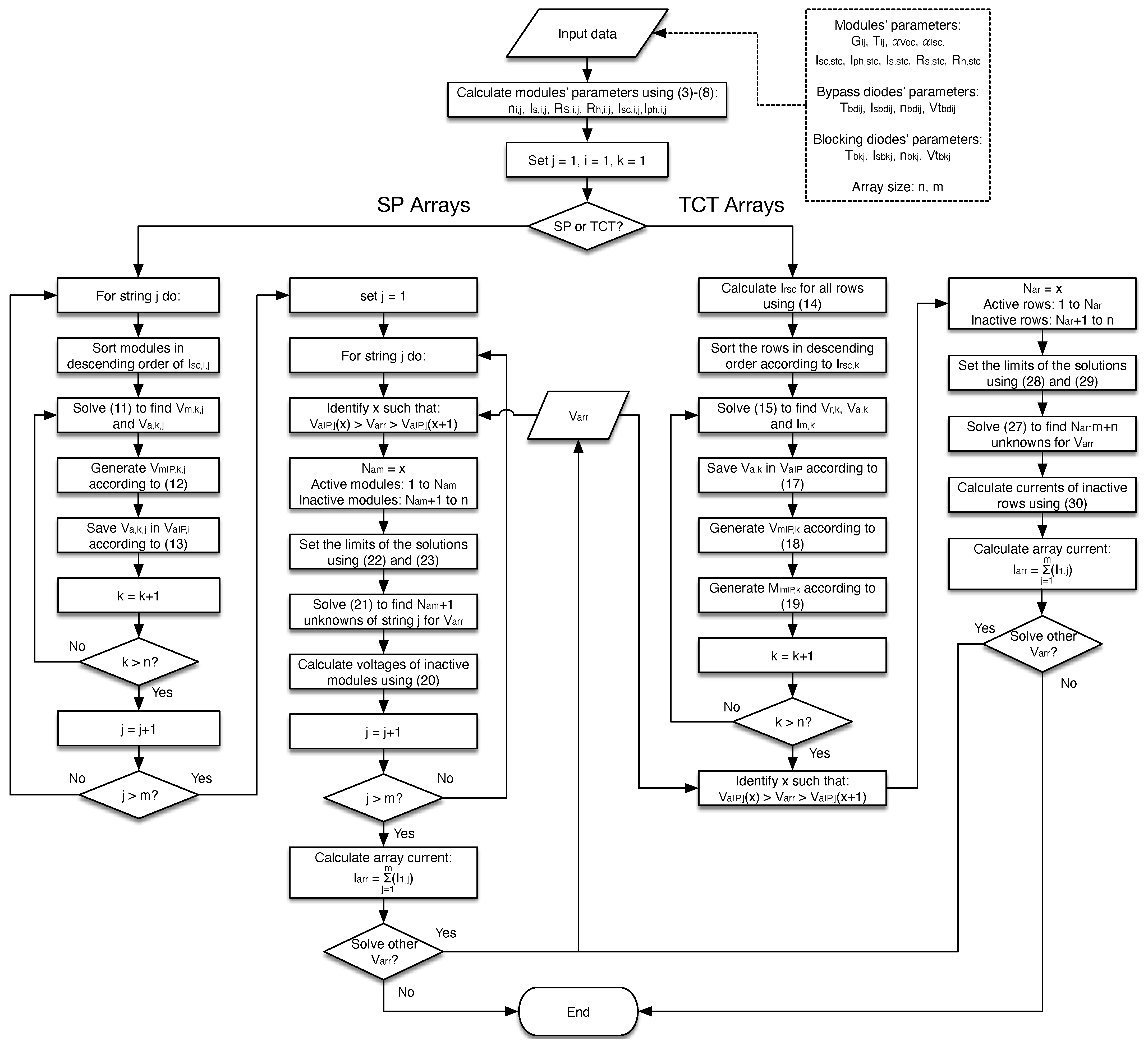
4.3. Summary of the Model Processing

To provide an easy-to-follow description of the model processing, Figure 10 presents a flowchart of the complete array current calculation ( I a r r ) for any voltage applied to the array terminals ( V a r r ). This flowchart can be followed to code the mathematical model in any programming language, for example, the simulation and experimental results of the following section were obtained by coding the model in Matlab.

5. Results

This section presents the results of the simulations and experiments performed to validate the proposed models. For simulation and experimental results, the PV module considered is the ERDM-85 [30], which has the following electrical characteristics: V o c , s t c = 21.78 V , V M P P , s t c = 17.95 V , I s c , s t c = 5.13 A , I M P P , s t c = 4.8 A , α I s c = 0.020 % / K , and α V o c = 0.34 % / K , where the subindex M P P indicates the maximum power point. Moreover, the results consider the systems of nonlinear equations proposed in [15] and [20] for SP and TCT arrays, respectively, as comparison solutions. Those papers propose mathematical models of the arrays based on the explicit function of the module current in terms of the voltage, which require the evaluation of the Lambert-W function, and any search range for the solution of the system of nonlinear equations is reported. Those models are referenced from here on as “Explicit”.
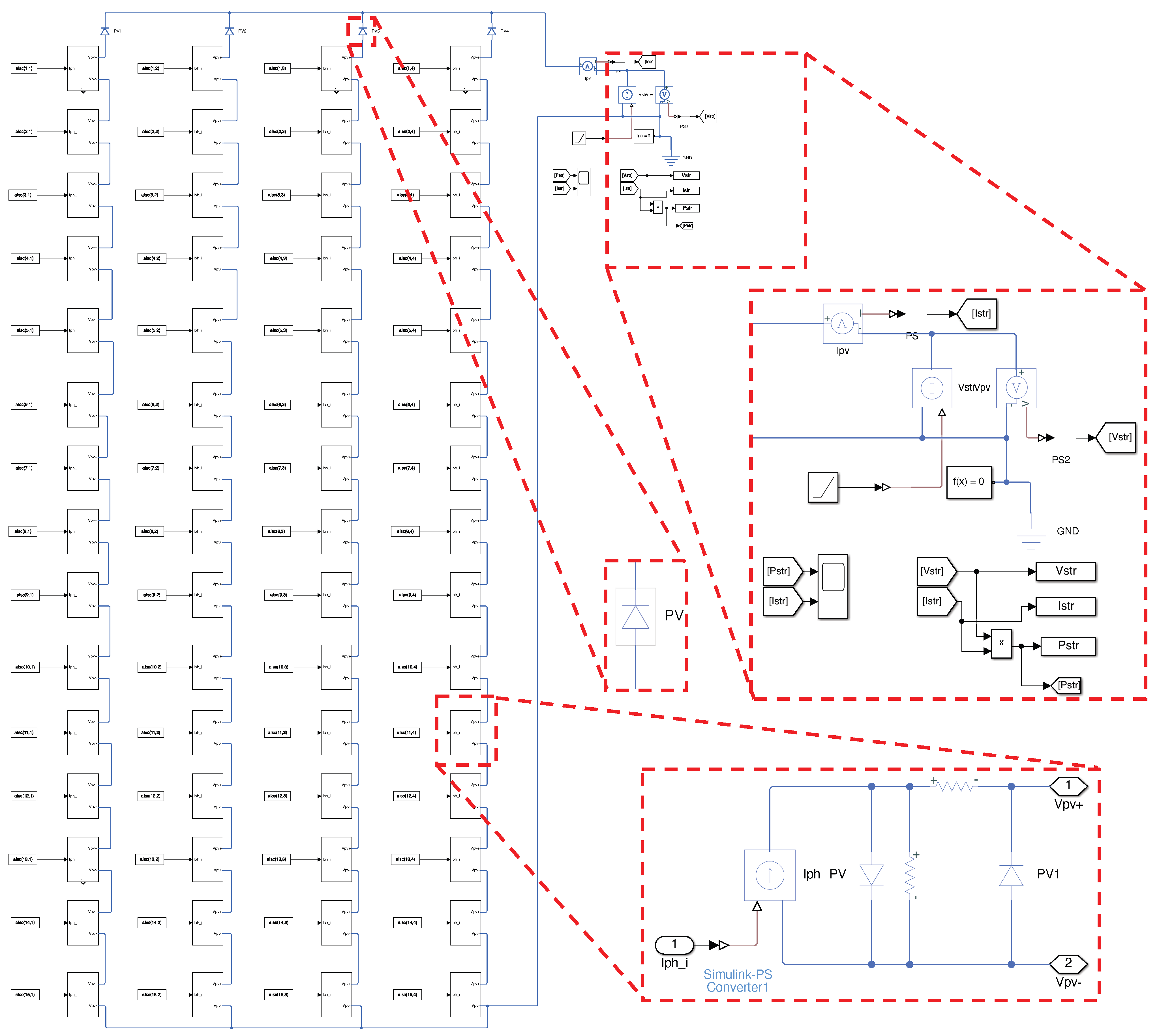
Section 5.1 reports the simulation results for a residential PV array considering the voltage and current restrictions of commercial inverters, considering both uniform and non-uniform operating conditions. Those results were obtained by implementing the proposed and explicit models in Matlab and comparing the results with the circuital implementation of the arrays in Matlab/Simulink. Such an equivalent circuit is obtained by implementing the SDM circuit of each module of the array; then, the I-V and P-V curves are obtained by performing a voltage sweep from V a r r = 0 V to V a r r = V o c V with fixed voltage steps (see Figure 11).
In addition, Section 5.2 shows the advantages of the proposed model for square PV arrays from 2 × 2 to 20 × 20 , and Section 5.3 shows an application example where both the proposed and explicit models are used for the reconfiguration of SP and TCT arrays. Finally, Section 5.4 reports the experimental validation of the modes using I-V curves generated from experimental measurements of the modules’ I-V curves at different operating conditions.

5.1. Example of PV Arrays for Residential Applications

For a residential PV array, the inverter SMA Sunny Boy 3.0 of 5.5 kWp is considered. This inverter can track the MPP between 110 V and 500 V ; therefore, it is defined n = 15 for SP and TCT arrays to obtain a nominal MPP voltage of 270 V , approximately. Furthermore, this inverter would handle four strings in parallel ( m = 4 ) considering its maximum power, the string voltage, and the I M P P , s t c of the ERDM 85 modules.
Applying the procedure proposed in [29], the following SDM parameters in STC are obtained: I p h , s t c = 5.13 A , η s t c = 1.0612 , I s , s t c = 1.1841 η A , R s , s t c = 0.1864 Ω , and R h , s t c = 261.0999 Ω . Then, the SDM parameters for G = 1.0 kW / m 2 and T = 45 C = 318.15 K are calculated by using Equations (3)–(8): I p h = 5.1544 A , η = 1.1324 , I s = 0.7497 η A , R s = 0.1989 Ω , and R h = 261.0999 Ω . Moreover, the bypass and blocking diodes are assumed to be equal, for the sake of simplicity, and with the following parameters: I s , b d = I s , b k = 1 μ A and η b d = η b k = 0.2694 ; however, it is important to mention that these parameters can be different, as explained in Section 2.1. Additionally, it is considered that the blocking diode is installed inside the junction box of a PV panel; hence, T b k T = 45 C = 318.15 K .
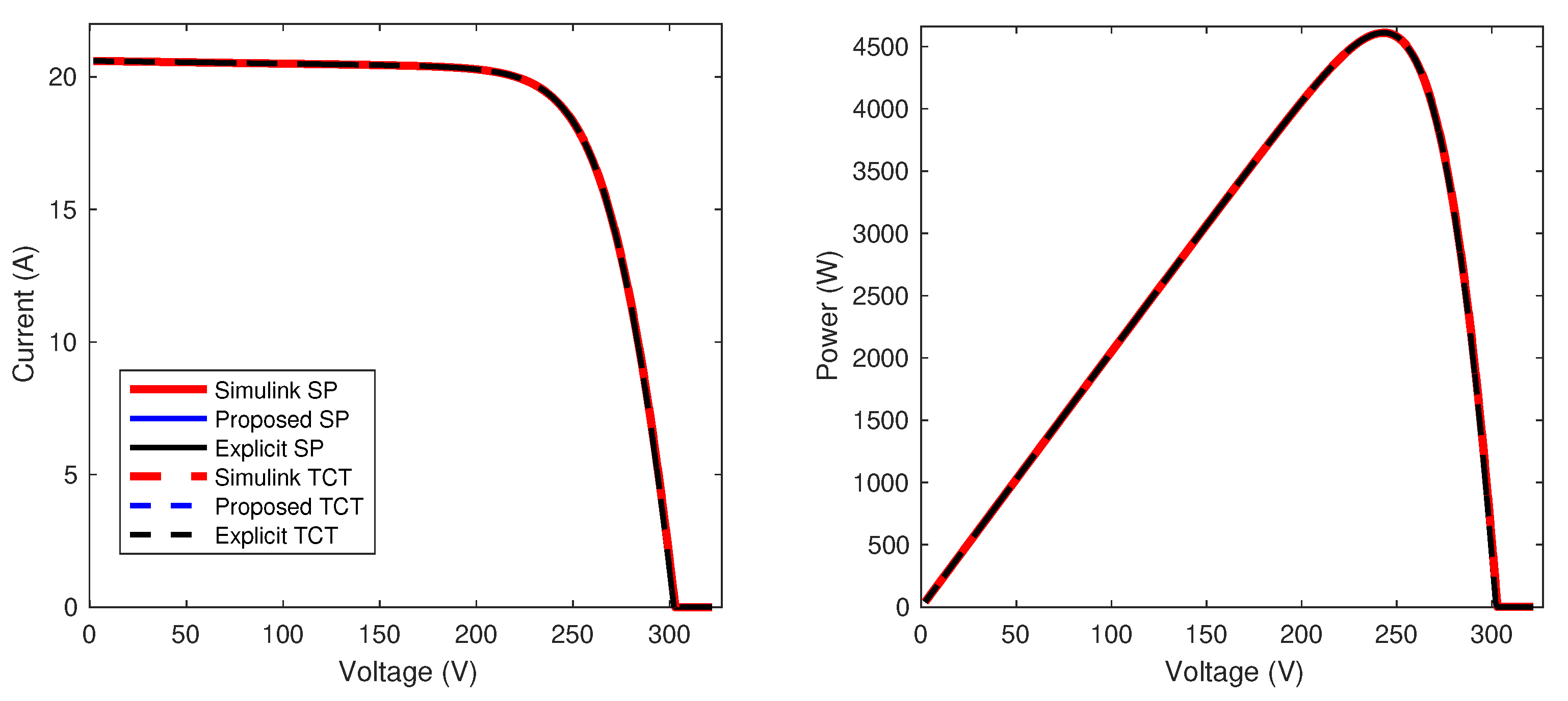
The 15 × 4 array is simulated considering SP and TCT configurations to generate the characteristic curves under both uniform conditions and non-uniform conditions with voltage steps of 1 V . Under uniform conditions, the characteristic curves are the same for both SP and TCT configurations (Figure 12) since the array behaves as a single module scaled in voltage by a factor n = 15 and scaled in current by a factor m = 4 . These operating conditions are difficult to obtain in real applications due to the shades generated by the surrounding objects, differences in the aging, and degradations of the modules that form a PV array. Therefore, the results shown from here on consider that the arrays operate under non-uniform conditions.
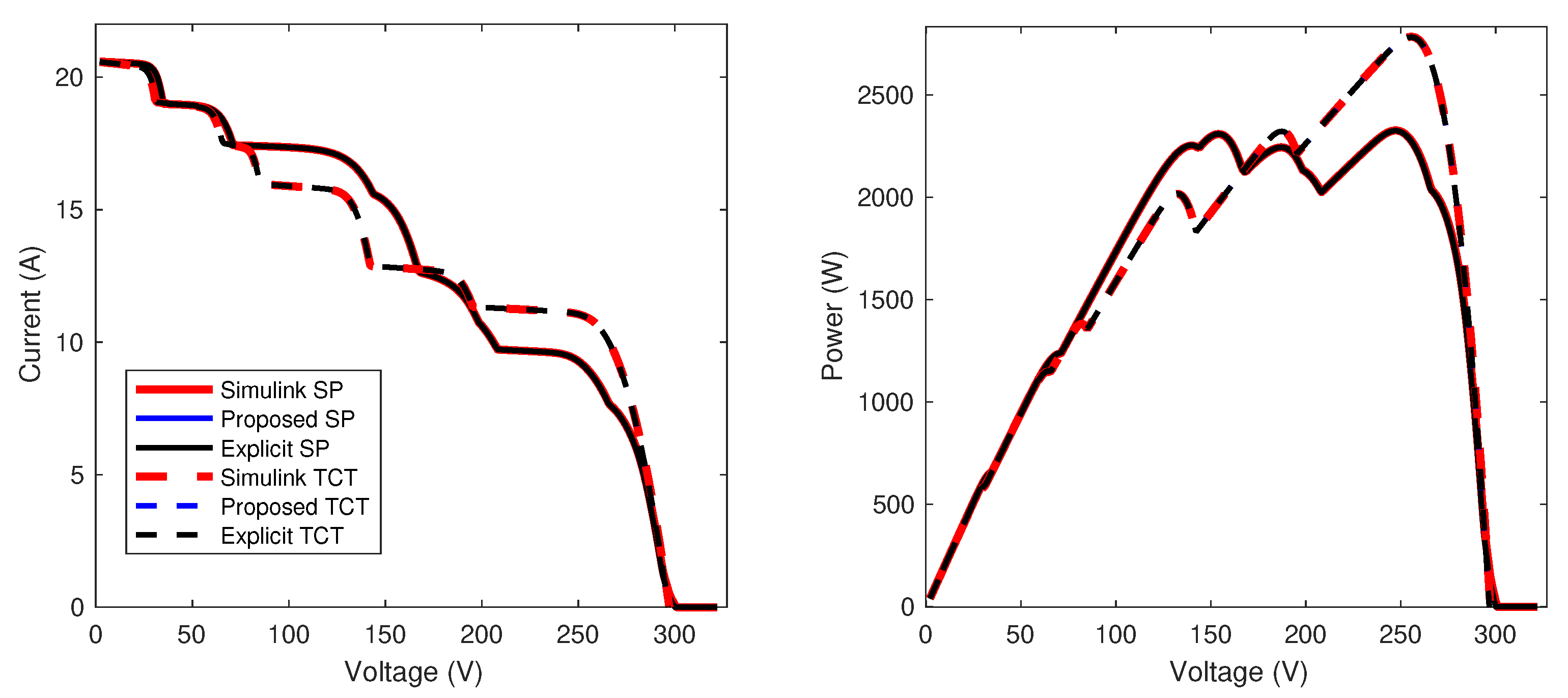
Figure 13 shows a shading pattern applied to the PV array, and Figure 14 reports the I-V and P-V curves for both the SP and TCT configurations. It is observed that the TCT array produces 19.66 % more power for this particular shading pattern. TCT configuration mitigates the power reduction produced by non-uniform conditions in this example. However, TCT is not the best configuration for any non-uniform condition since the best configuration depends on the particular shading pattern as shown in [9,22].
Figure 12 and Figure 14 also show that all of the proposed and explicit models provide the same characteristic curves for both the SP and TCT configurations. Then, they are evaluated five times to determine the average calculation time of each solution, its standard deviation, and the normalized sum of squared errors (NSSE), and they are also calculated for the SP and TCT array operating under non-uniform conditions. The results of such a test are summarized in Table 1 for both the SP and TCT arrays.
The proposed and comparison (explicit) models are solved by using the “fmincon” function of Matlab, which allows for the definition of upper and lower bounds for the solution of a nonlinear system of equations by applying the procedure proposed in Section 4. Table 1 shows that the calculation time of the proposed model is lower than the other solutions. Regarding the proposed model, the simulation time of the circuital implementation (Simulink) is 3.0 and 1.6 times longer for SP and TCT configurations, respectively, while the calculation times of the explicit model are 9.5 and 12.7 times longer for the explicit model in SP and TCT configurations, respectively. Hence, the results reported in this section confirm that the proposed model, based on the implicit equations and the definition of the solution bounds for the system of nonlinear equations, significantly reduce the calculation times.

5.2. Time Reduction and Current Errors for Different Array Sizes

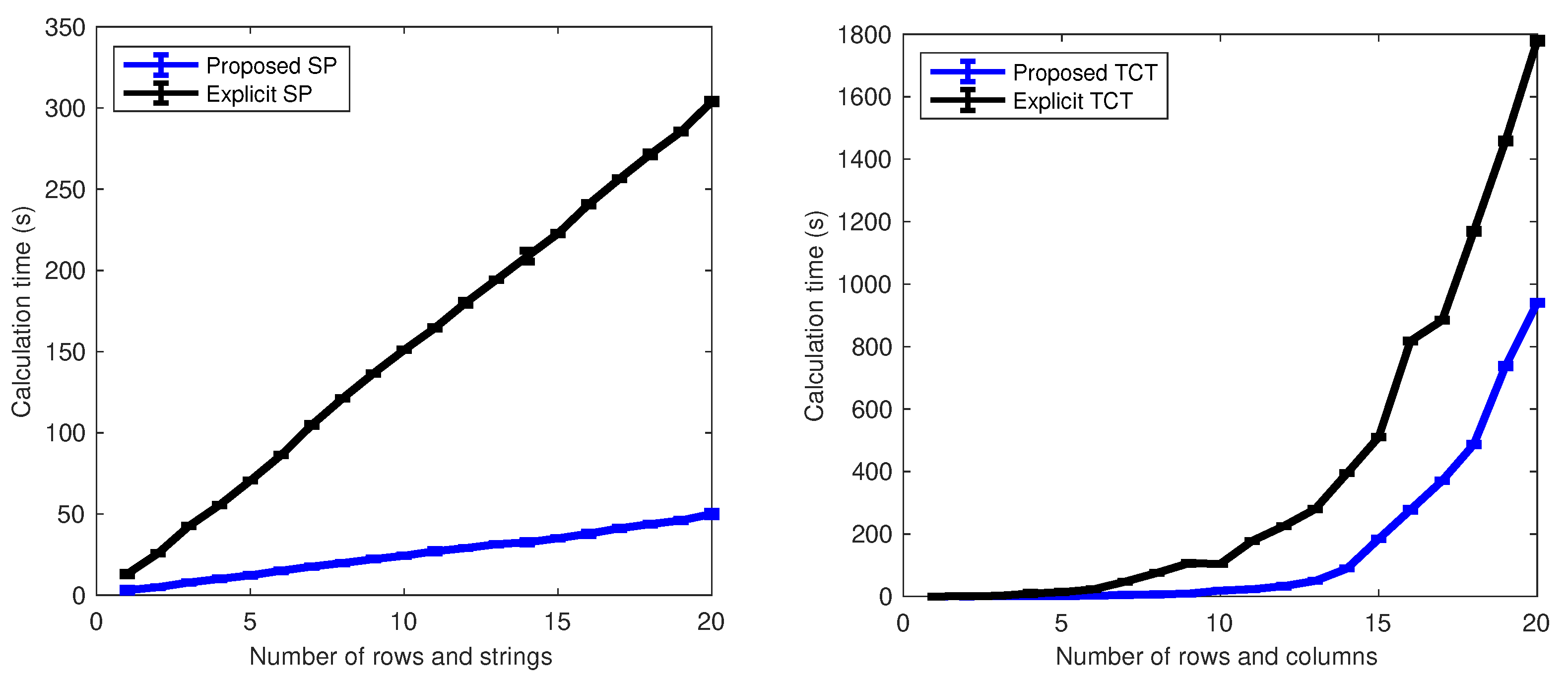
This section compares the calculation time and current error of the proposed model for square SP and TCT arrays with sizes from 2 × 2 (4 modules) to 20 × 20 (400 modules). In this case, the simulations generate the characteristic curves of the arrays with voltage steps of 1.977 V , and each curve is calculated five times to determine the average calculation time. The average solution time and the standard deviation are illustrated in Figure 15, where the increment of the calculation time for SP and TCT arrays regarding the dimension of the square array can be observed. The time reduction in the proposed model is 82.97 % on average for SP arrays. For TCT arrays, the time reduction varies between 46.71 % and 92.28 % for arrays from 3 × 3 onwards; the explicit TCT model is faster only for the smallest array ( 2 × 2 ). Therefore, the speed improvement provided by the proposed solutions for any SP array is confirmed, and for any TCT array larger than 2 × 2 .
Additionally, the equivalent circuits of the arrays were implemented in Simulink to calculate the errors in the array’s current calculation. Such errors are introduced in Figure 16 for SP and TCT arrays and are almost the same for explicit and proposed models. On the one hand, in SP arrays the largest errors are for 3 × 3 and 2 × 2 , respectively, while for the other arrays, the current error presents a growth tendency with the array size. On the other hand, in TCT arrays the largest errors are for 4 × 4 to 10 × 10 arrays with the maximum error in 9 × 9 array. Moreover, for these arrays, the errors for arrays from 12 × 12 to 20 × 20 do not change considerably.

5.3. Application Example: A Model-Based Reconfiguration of TCT and SP Arrays

Partial shading conditions change throughout the day; thus, the optimal configuration that produces the highest power also changes continuously. Therefore, a dynamic reconfiguration of the PV array (or part of the array), searching for the optimal structure every hour or less, has been used to improve the array power production throughout the day [32], thus improving the array profitability. Some works have focused on improving the reconfiguration speed by optimizing the algorithm used to search for the best configuration [33], which enables the optimization of the array more times per day; however, those works are limited by the calculation speed of the mathematical model used to reproduce the P-V curve. Therefore, the reduction in the calculation time required by the proposed model to generate the array’s P-V curves is very useful for reconfiguration systems, which is illustrated in this example.
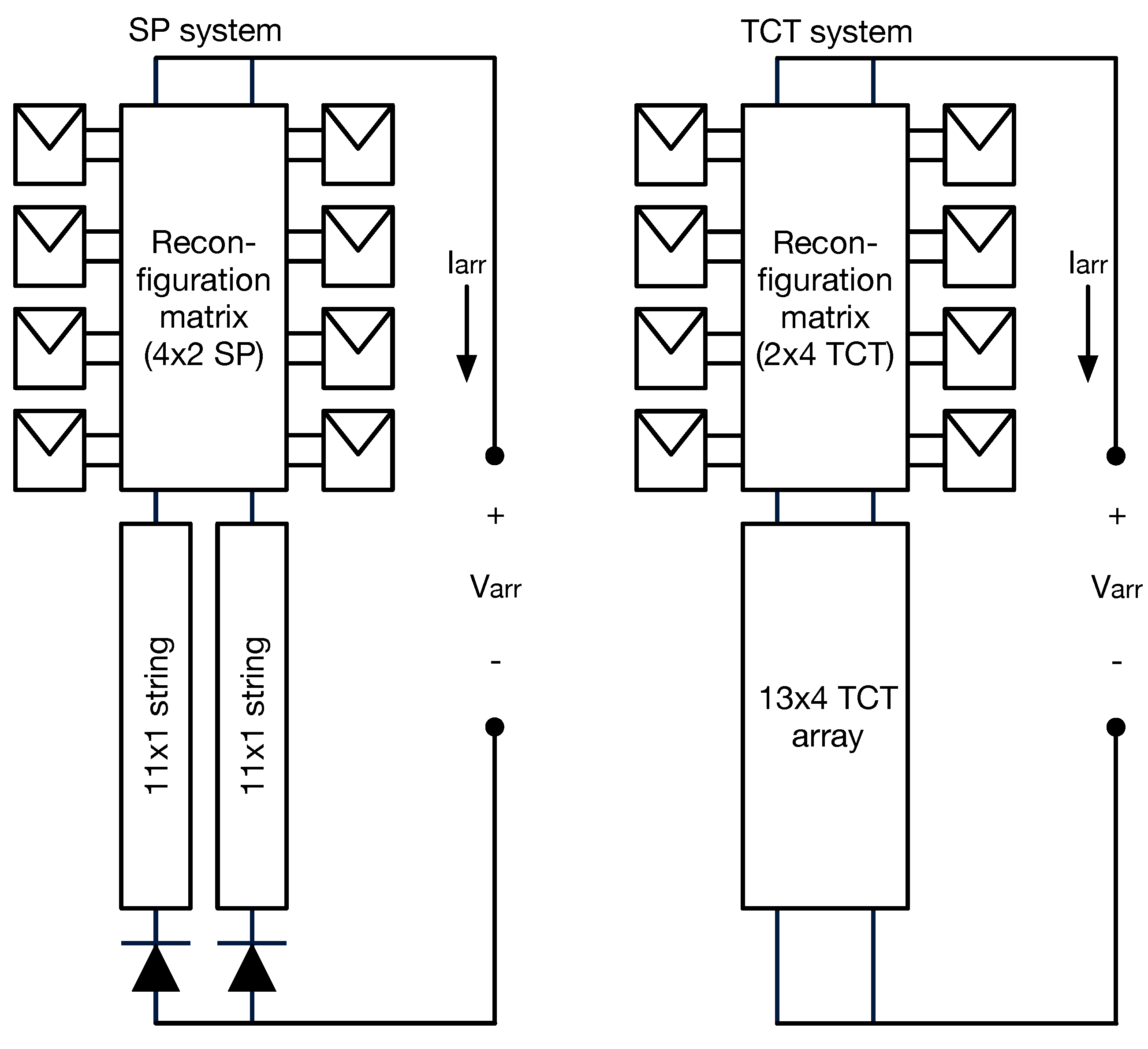
The SP and TCT arrays considered in this section for reconfiguration are illustrated in Figure 17, where a part of the modules in the array has a fixed connection, while the connections of another part of the array (eight modules) can be reconfigured (change the connections). This partial reconfiguration approach has also been used in other studies [34]. On the one hand, the SP array is 15 × 2 , and the first four rows ( 4 × 2 ) can be connected to any string through a reconfiguration matrix, which is implemented with switches (e.g., MOSFETs or relays) and controlled by a reconfiguration algorithm [35]. On the other hand, the TCT array is 15 × 4 , where the modules in the first two rows ( 2 × 4 ) can be connected to any row by using a reconfiguration matrix and a reconfiguration algorithm.
The reconfiguration algorithm considered for this application example is an exhaustive search, where all of the possible configurations are evaluated. For each configuration, the array P-V curve is generated with voltage steps of 2 V to identify the GMPP, which is saved to identify the configuration that provides the highest GMPP. Then, the reconfiguration matrix is adjusted to realize the best configuration. This process must be repeated as fast as possible to improve the energy harvesting from a PV array operating under non-uniform conditions since those conditions continuously change throughout the day.
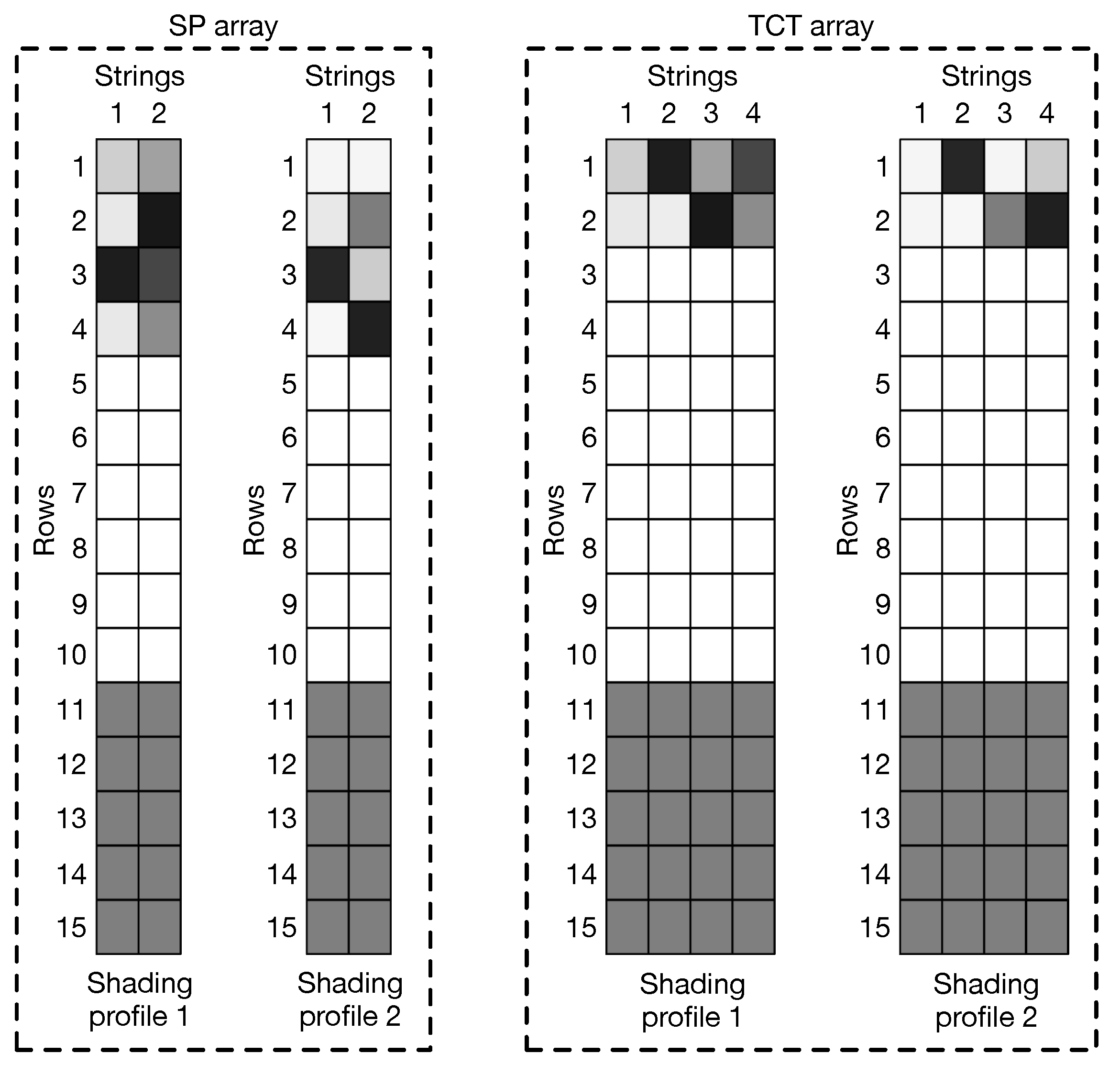
This application example considers two shading profiles for each array, which are illustrated in Figure 18 for the SP and TCT arrays, respectively. Those profiles are defined by specifying the parameter I p h for the reconfigurable modules, where Table 2 and Table 3 report the shading factors (1 means no shading, 0 means full shading). The photovoltaic current I p h of the rest of the modules of the SP and TCT arrays is defined as follows:
  • SP array: I p h , a , b = 5.154 A a [ 5 , , 10 ] b [ 1 , 2 ] and I p h , c , b = 2.577 A c [ 11 , , 15 ] b [ 1 , 2 ]
  • TCT array: I p h , a , b = 5.154 A a [ 3 , , 9 ] b [ 1 , , 4 ] and I p h , c , b = 2.577 A c [ 10 , , 15 ] b [ 1 , , 4 ]
For both arrays, there are 35 possible configurations with the eight reconfigurable modules; therefore, all of the configurations are evaluated, for each array and shading profile, with both the proposed and explicit models to determine their calculation times. The results are reported in Table 4, where it is observed that the times required by the proposed models are around 3.9 and 11.3 min for SP and TCT arrays, respectively, while the times required by the explicit models are around 28.8 and 54.4 min. Hence, the proposed models provide a reduction between 78 % and 86 % of the time required to evaluate the 35 configurations of the SP and TCT arrays. Such time reduction means that the reconfiguration algorithm using the proposed models can better mitigate the power reduction produced by the variable shading profiles throughout the day and, as consequence, improve the power and energy harvesting.

5.4. Experimental Results

The proposed models were experimentally validated with 4 × 2 (i.e., eight modules) SP and TCT arrays operating under two different conditions denominated “Experiment 1” and “Experiment 2” from here on. The I-V and P-V array curves were generated by interpolating the experimental I-V curves of eight modules. The I-V curves of the SP arrays were obtained by interpolating the voltage of each module for a set of given string currents and adding the modules’ voltages to obtain V a r r ; then, the array currents were calculated by interpolating the current of each string for a given array voltage. For TCT, the I-V curves were obtained by interpolating the current of each module for a set of given row voltages and adding the modules’ currents to obtain I a r r ; then, the array voltages were calculated by interpolating the voltage of each row for a given array current.
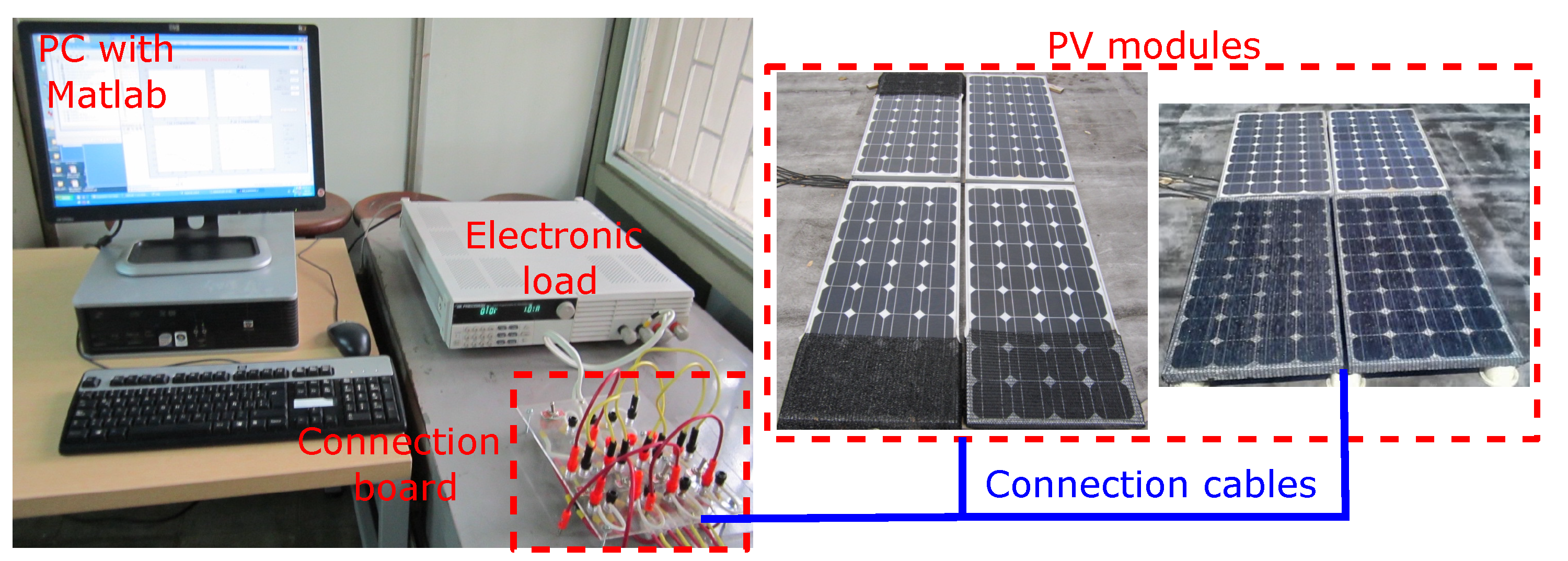
The I-V curve of each module was measured through a BK 8500 electronic load by using the experimental testbed shown in Figure 19. Each module’s I-V curve is formed by 108 points, and the array’s I-V curve is formed by 400 points, approximately.
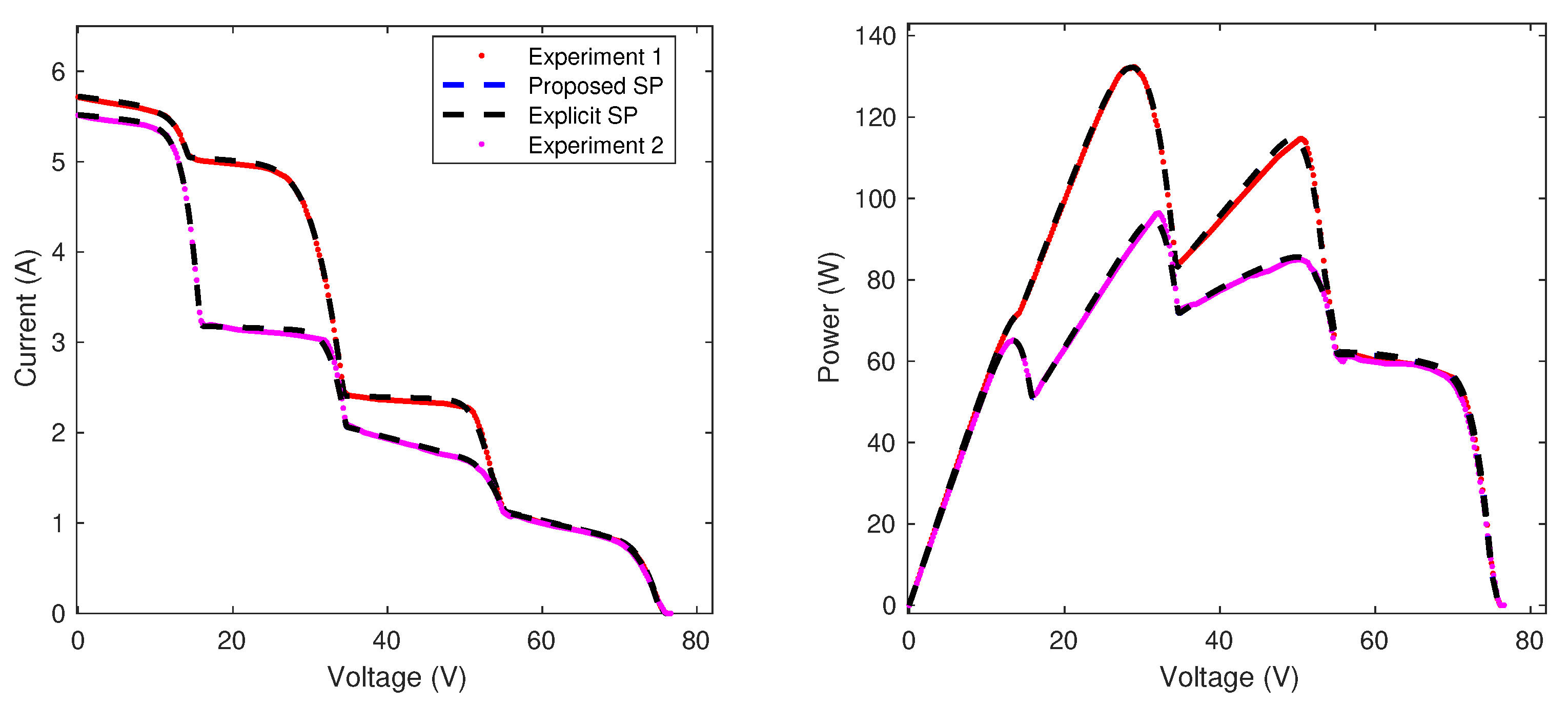
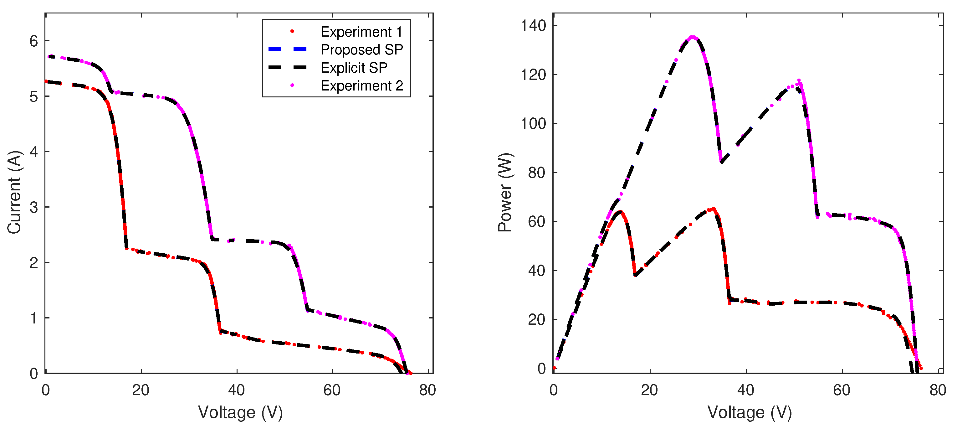
The characteristic curves of the SP and TCT arrays for the two experiments are introduced in Figure 20 and Figure 21, respectively, where the dashed lines represent the explicit and proposed models, and the dots represent the experimental measurements. Both figures present the I-V and P-V curves for arrays, which are presented at the left and right, respectively, and it can be observed that the dots are superimposed on the dashed lines, which means that the proposed models accurately reproduce the electrical behavior of the SP and TCT arrays for the two experiments. Such accurate reproduction is verified through the NSSE errors of both models (see Table 5), which are practically the same for the proposed and explicit models because both models used the same SDM parameters for all of the modules. However, significant differences are present in the calculation times, where the proposed model obtains reductions between 65 and 72 % regarding the explicit model. Therefore, this experimental validation confirms the advantage of the proposed model over the explicit ones and provides the same accuracy but with a much higher calculation speed (more than 3 times faster).

6. Conclusions

This paper has presented a mathematical model for both SP and TCT PV arrays based on the implicit equations of the SDM and the inflection points of the current–voltage curves, which significantly speeds up the calculation process in comparison with the traditional explicit models based on the Lambert-W function. This feature was tested in several simulation scenarios with multiple array sizes, where the results show that the proposed SP model is always faster than the traditional solution, reducing the computation time by 82.97%. Concerning the proposed TCT model, it is faster for arrays larger than 2 × 2 , providing reduction times between 47.71% and 92.28%. For arrays 2 × 2 , the classical TCT model is slightly faster, but taking into account that 2 × 2 arrays only have three possible configurations, those can be tested very fast with either the proposed or the explicit model. Therefore, the proposed model can be used to speed up the design of urban PV installations subjected to partial shading conditions since the yearly power production of large PV arrays can be estimated in a short time and with high precision.
The proposed solution was also tested for dynamic reconfiguration purposes, where both SP and TCT arrays were partially reconfigured to improve power production under two partial-shading conditions. The results demonstrate that the proposed solution provides the same optimal configuration (hence the same maximum PV power) but more than 7 times faster for SP reconfigurations, and between 4 and 6 times faster for TCT reconfigurations. This is very useful in practical applications since a faster reconfiguration enables the optimization of more times the array configuration to the changing non-homogenous conditions, thus improving the energy harvesting throughout the day and reducing the return-of-the-investment time. The improved speed and high accuracy of the proposed model were also validated using experimental data. The experimental results demonstrate that the proposed solution provides the same accuracy as the classical (explicit) solutions, but it is more than 3 times faster.
The proposed model shares a particular drawback with the explicit model reported in the literature: requiring a solver for the non-linear equations system, which can be improved in two ways. The first approach could be to mathematically derive the Jacobian matrix of the system of equations, thus using it to speed up the solver. This can be further improved by obtaining an analytical inversion of the Jacobian matrix, which requires deep mathematical analysis but can significantly improve the performance of the equation solver. However, it is not certain that the Jacobian matrix could be analytically inverted for any shading profile. The second approach could be to solve, symbolically, the non-linear equations system; this will require deep non-linear analyses and maybe some well-guessed approximations, but it is not certain that the nonlinear equations system has analytical solutions for every shading condition. However, the success of this process could exponentially improve the solution time. Therefore, both approaches are interesting topics for further development.

Author Contributions

Conceptualization, methodology, software, and writing (review and editing): C.A.R.-P., J.D.B.-R. and A.J.S.-M. All authors have read and agreed to the published version of the manuscript.

Funding

This research was funded by Minciencias, Universidad Nacional de Colombia, Universidad del Valle, and Instituto Tecnológico Metropolitano under the research project “Dimensionamiento, planeación y control de sistemas eléctricos basados en fuentes renovables no convencionales, sistemas de almacenamiento y pilas de combustible para incrementar el acceso y la seguridad energética de poblaciones colombianas” (Minciencias code 70386), which belongs to the research program “Estrategias para el desarrollo de sistemas energéticos sostenibles, confiables, eficientes y accesibles para el futuro de Colombia” (Minciencias code 1150-852-70378, Hermes code 46771).

Data Availability Statement

The data used in this study are reported in the paper figures and tables.

Conflicts of Interest

The authors declare no conflict of interest.

References

  1. IEA. Snapshot of Global PV Markets 2023; Technical Report; International Energy Agency: Paris, France, 2023. [Google Scholar]
  2. Dessouky, S.S.; Elbaset, A.A.; Alaboudy, A.H.; Ibrahim, H.A.; Abdelwahab, S.A. Performance Improvement of a PV-Powered Induction-Motor-Driven Water Pumping System. In Proceedings of the 2016 18th International Middle-East Power Systems Conference, Cairo, Egypt, 27–29 December 2016; pp. 373–379. [Google Scholar] [CrossRef]
  3. Elbaset, A.A.; Abdelwahab, S.A.M.; Ibrahim, H.A.; Eid, M.A.E. Performance Analysis of Photovoltaic Systems with Energy Storage Systems; Springer: Berlin/Heidelberg, Germany, 2019; pp. 1–253. [Google Scholar] [CrossRef]
  4. Elnozahy, A.; Yousef, A.M.; Ghoneim, S.S.; Abdelwahab, S.A.; Mohamed, M.; Abo-Elyousr, F.K. Optimal Economic and Environmental Indices for Hybrid PV/Wind-Based Battery Storage System. J. Electr. Eng. Technol. 2021, 16, 2847–2862. [Google Scholar] [CrossRef]
  5. Elnozahy, A.; Yousef, A.M.; Abo-Elyousr, F.K.; Mohamed, M.; Abdelwahab, S.A. Performance improvement of hybrid renewable energy sources connected to the grid using artificial neural network and sliding mode control. J. Power Electron. 2021, 21, 1166–1179. [Google Scholar] [CrossRef]
  6. Mohamed Abdelwahab, S.A.; Hamada, A.M.; Abdellatif, W.S. Comparative analysis of the modified perturb & observe with different MPPT techniques for PV grid connected systems. Int. J. Renew. Energy Res. 2020, 10, 155–164. [Google Scholar] [CrossRef]
  7. Yousef, A.M.; Ebeed, M.; Abo-Elyousr, F.K.; Elnozohy, A.; Mohamed, M.; Mohamed Abdelwahab, S.A. Optimization of PID controller for Hybrid Renewable Energy System using Adaptive Sine Cosine Algorithm. Int. J. Renew. Energy Res. 2020, 10, 669–677. [Google Scholar] [CrossRef]
  8. Pachauri, R.; Singh, R.; Gehlot, A.; Samakaria, R.; Choudhury, S. Experimental analysis to extract maximum power from PV array reconfiguration under partial shading conditions. Eng. Sci. Technol. Int. J. 2019, 22, 109–130. [Google Scholar] [CrossRef]
  9. Saeed, F.; Tauqeer, H.A.; Gelani, H.E.; Yousuf, M.H.; Idrees, A. Numerical modeling, simulation and evaluation of conventional and hybrid photovoltaic modules interconnection configurations under partial shading conditions. EPJ Photovolt. 2022, 13, 10. [Google Scholar] [CrossRef]
  10. Petrone, G.; Ramos-Paja, C.A.; Spagnuolo, G. Photovoltaic Sources Modeling; John Wiley & Sons, Ltd.: Chichester, UK, 2017. [Google Scholar] [CrossRef]
  11. Khan, F.U.; Murtaza, A.F.; Sher, H.A.; Al-Haddad, K.; Mustafa, F. Cabling constraints in PV array architecture: Design, mathematical model and cost analysis. IEEE Access 2020, 8, 182742–182754. [Google Scholar] [CrossRef]
  12. Petrone, G.; Spagnuolo, G.; Vitelli, M. Analytical model of mismatched photovoltaic fields by means of Lambert W-function. Sol. Energy Mater. Sol. Cells 2007, 91, 1652–1657. [Google Scholar] [CrossRef]
  13. Bastidas-Rodriguez, J.D.; Cruz-Duarte, J.M.; Correa, R. Mismatched Series–Parallel Photovoltaic Generator Modeling: An Implicit Current–Voltage Approach. IEEE J. Photovolt. 2019, 9, 768–774. [Google Scholar] [CrossRef]
  14. Jha, V. Comprehensive Modeling and Simulation of PV Module and Different PV Array Configurations Under Partial Shading Condition. Iran. J. Sci. Technol. Trans. Electr. Eng. 2022, 46, 503–535. [Google Scholar] [CrossRef]
  15. Orozco-Gutierrez, M.L.; Ramirez-Scarpetta, J.M.; Spagnuolo, G.; Ramos-Paja, C.A. A technique for mismatched PV array simulation. Renew. Energy 2013, 55, 417–427. [Google Scholar] [CrossRef]
  16. Bastidas, J.D.; Franco, E.; Petrone, G.; Ramos-Paja, C.A.; Spagnuolo, G. A model of photovoltaic fields in mismatching conditions featuring an improved calculation speed. ELectric Power Syst. Res. 2013, 96, 81–90. [Google Scholar] [CrossRef]
  17. Pérez-Archila, L.M.; Rodriguez Bastidas, J.D.; Correa, R. Solución del modelo de un generador fotovoltaico utilizando los algoritmos de optimización Trust Region Dogleg y PSO. Rev. Uis Ing. 2020, 19, 37–48. [Google Scholar] [CrossRef]
  18. Petrone, G.; Ramos-Paja, C. Modeling of photovoltaic fields in mismatched conditions for energy yield evaluations. Electr. Power Syst. Res. 2011, 81, 1003–1013. [Google Scholar] [CrossRef]
  19. Pérez Archila, L.M.; Bastidas-Rodríguez, J.D.; Correa, R.; Trejos Grisales, L.A.; Gonzalez-Montoya, D. A Solution of Implicit Model of Series-Parallel Photovoltaic Arrays by Using Deterministic and Metaheuristic Global Optimization Algorithms. Energies 2020, 13, 801. [Google Scholar] [CrossRef] [Green Version]
  20. Orozco-Gutierrez, M.L.; Spagnuolo, G.; Ramos-Paja, C.A.; Ramirez-Scarpetta, J.M.; Ospina-Agudelo, B. Enhanced simulation of total cross tied photovoltaic arrays. Math. Comput. Simul. 2019, 158, 49–64. [Google Scholar] [CrossRef]
  21. Ramos-Paja, C.A.; Bastidas-Rodríguez, J.D.; Saavedra-Montes, A.J. Experimental Validation of a Model for Photovoltaic Arrays in Total-Cross-Tied Configuration. Dyna 2013, 80, 191–199. [Google Scholar]
  22. Mohammadnejad, S.; Khalafi, A.; Ahmadi, S.M. Mathematical analysis of total-cross-tied photovoltaic array under partial shading condition and its comparison with other configurations. Sol. Energy 2016, 133, 501–511. [Google Scholar] [CrossRef]
  23. Jha, V. Mathematical modelling of PV array under partial shading condition. Sadhana Acad. Proc. Eng. Sci. 2022, 47, 85. [Google Scholar] [CrossRef]
  24. Nnamchi, S.N.; Oko, C.O.; Kamen, F.L.; Sanya, O.D. Mathematical analysis of interconnected photovoltaic arrays under different shading conditions. Cogent Eng. 2018, 5, 1507442. [Google Scholar] [CrossRef]
  25. Ko, S.W.; Ju, Y.C.; Hwang, H.M.; So, J.H.; Jung, Y.S.; Song, H.J.; Eun Song, H.; Kim, S.H.; Kang, G.H. Electric and thermal characteristics of photovoltaic modules under partial shading and with a damaged bypass diode. Energy 2017, 128, 232–243. [Google Scholar] [CrossRef]
  26. De Soto, W.; Klein, S.; Beckman, W. Improvement and validation of a model for photovoltaic array performance. Sol. Energy 2006, 80, 78–88. [Google Scholar] [CrossRef]
  27. Villalva, M.; Gazoli, J.; Filho, E. Comprehensive Approach to Modeling and Simulation of Photovoltaic Arrays. IEEE Trans. Power Electron. 2009, 24, 1198–1208. [Google Scholar] [CrossRef]
  28. Bai, J.; Liu, S.; Hao, Y.; Zhang, Z.; Jiang, M.; Zhang, Y. Development of a new compound method to extract the five parameters of PV modules. Energy Convers. Manag. 2014, 79, 294–303. [Google Scholar] [CrossRef]
  29. Accarino, J.; Petrone, G.; Ramos-Paja, C.A.; Spagnuolo, G. Symbolic Algebra for the Calculation of the Series and Parallel Resistances in PV Module Model. In Proceedings of the 2013 International Conference on Clean Electrical Power (ICCEP), Alghero, Italy, 11–13 June 2013; pp. 62–66. [Google Scholar] [CrossRef]
  30. ERDM Solar. Datasheet ERDM 75–85 W. 2023. Available online: https://es.enfsolar.com/pv/panel-datasheet/crystalline/19863 (accessed on 20 April 2023).
  31. Trejos-Grisales, L.A.; Bastidas-Rodríguez, J.D.; Ramos-Paja, C.A. Mathematical model for regular and irregular PV arrays with improved calculation speed. Sustainability 2020, 12, 10684. [Google Scholar] [CrossRef]
  32. Spagnuolo, G.; Petrone, G.; Lehman, B.; Ramos-Paja, C.; Zhao, Y.; Orozco Gutierrez, M. Control of Photovoltaic Arrays: Dynamical Reconfiguration for Fighting Mismatched Conditions and Meeting Load Requests. IEEE Ind. Electron. Mag. 2015, 9, 62–76. [Google Scholar] [CrossRef]
  33. Orozco-Gutierrez, M.L.; Spagnuolo, G.; Ramirez-Scarpetta, J.M.; Petrone, G.; Ramos-Paja, C.A. Optimized Configuration of Mismatched Photovoltaic Arrays. IEEE J. Photovoltaics 2016, 6, 1210–1220. [Google Scholar] [CrossRef]
  34. Velasco-Quesada, G.; Guinjoan-Gispert, F.; Pique-Lopez, R.; Roman-Lumbreras, M.; Conesa-Roca, A. Electrical PV Array Reconfiguration Strategy for Energy Extraction Improvement in Grid-Connected PV Systems. IEEE Trans. Ind. Electron. 2009, 56, 4319–4331. [Google Scholar] [CrossRef] [Green Version]
  35. Osmani, K.; Haddad, A.; Jaber, H.; Lemenand, T.; Castanier, B.; Ramadan, M. Mitigating the effects of partial shading on PV system’s performance through PV array reconfiguration: A review. Therm. Sci. Eng. Prog. 2022, 31, 101280. [Google Scholar] [CrossRef]
Figure 1. n × m PV arrays with SP (top) and TCT (bottom) configurations.
Energies 16 04875 g001
Figure 2. Single-diode model of a PV module.
Energies 16 04875 g002
Figure 3. I-V and P-V curve generation.
Energies 16 04875 g003
Figure 4. Example of generation of V m I P , j and V a I P , j for a 3 × 1 SP array.
Energies 16 04875 g004
Figure 5. Example of generation of V m I P , k , M i m I P , k , and V a I P for a 3 × 2 TCT array.
Energies 16 04875 g005
Figure 6. Simplified representation of a string with N a m active modules and n N a m inactive modules.
Energies 16 04875 g006
Figure 7. Example of definition of x and N a m for an arbitrary value of V a r r for a string with three modules and one blocking diode.
Energies 16 04875 g007
Figure 8. Simplified representation of a TCT array N a m active rows and n N a m inactive rows.
Energies 16 04875 g008
Figure 9. Example of definition of x and N a r for an arbitrary value of V a r r for an 3 × 2 TCT array.
Energies 16 04875 g009
Figure 10. Flowchart of the model processing.
Energies 16 04875 g010
Figure 11. Example of 15 × 4 SP array implemented in Simulink to generate I-V and P-V curves. It shows a zoom for single-diode model, blocking diode, and voltage source used to perform the voltage sweep.
Energies 16 04875 g011
Figure 12. I-V and P-V curves for SP and TCT arrays operating under uniform conditions.
Energies 16 04875 g012
Figure 13. Shading pattern for SP and TCT arrays operating under non-uniform conditions.
Energies 16 04875 g013
Figure 14. I-V and P-V curves for SP and TCT arrays operating under non-uniform conditions.
Energies 16 04875 g014
Figure 15. Calculation time of square SP (left) and TCT (right) arrays from 2 × 2 to 20 × 20 .
Energies 16 04875 g015
Figure 16. Array current NSSE for square SP (left) and TCT (right) arrays from 2 × 2 to 20 × 20 .
Energies 16 04875 g016
Figure 17. SP and TCT reconfiguration systems used for the application example.
Energies 16 04875 g017
Figure 18. Shading profiles to evaluate the reconfiguration.
Energies 16 04875 g018
Figure 19. Test bed used to measure the I-V curves of the PV modules.
Energies 16 04875 g019
Figure 20. I-V and P-V curves for two experiments of 4 × 2 SP arrays operating under different conditions.
Energies 16 04875 g020
Figure 21. I-V and P-V curves for two experiments of 4 × 2 TCT arrays operating under different conditions.
Energies 16 04875 g021
Table 1. Calculation time of 15 × 4 SP and TCT arrays operating under non-uniform conditions.
SPTCT
ModelAverage (s)Std (s)NSSE (%)Average (s)Std (s)NSSE (%)
Simulink58.1240.278N.A.54.6340.514N.A.
Proposed19.2900.126 0.96 ×   10 5 33.8770.315 1.01 ×   10 5
Explicit183.6961.342 0.95 ×   10 5 431.6393.655 0.93 ×   10 5
Table 2. Shading profiles of the reconfigurable modules of the SP array (1 means no shading).
ArrayShading ProfileRowColumn
12
SP110.81470.6324
20.90580.0975
30.12700.2785
40.91340.5469
210.95750.9572
20.96490.4854
30.15760.8003
40.97060.1419
Table 3. Shading profiles of the reconfigurable modules of the TCT array (1 means no shading).
ArrayShading ProfileRowColumn
1234
TCT110.81470.12700.63240.2785
20.90580.91340.09750.5469
210.95750.15760.95720.8003
20.96490.97060.48540.1419
Table 4. Calculation times, time reduction, and power increment calculated with proposed and explicit models to evaluate all of the possible configurations (i.e., 35) for the shading profiles of SP and TCT arrays.
ArrayProfileCalculation Times (s)Time Reduction (%)Power Increment (%)
ProposedExplicit
SP1236.71728.286.39.09
2216.31602.586.57.66
TCT1536.03264.183.56.37
2680.33199.778.75.16
Table 5. Calculation times, time reduction, and power increment calculated with proposed and explicit models to evaluate all of the possible configurations (i.e., 35) for the shading profiles of SP and TCT arrays.
ArrayExperimentNSSE (%)Calculation Time (s)Time Reduction (%)
ProposedExplicitProposedExplicit
SP15.00 ×   10 3 5.00 ×   10 3 9.29626.65865.1
28.93 ×   10 3 8.92 ×   10 3 8.39230.62172.5
TCT12.85 ×   10 2 2.86 ×   10 2 4.90016.71767.3
24.05 ×   10 3 4.06 ×   10 3 5.672317.38570.6
Disclaimer/Publisher’s Note: The statements, opinions and data contained in all publications are solely those of the individual author(s) and contributor(s) and not of MDPI and/or the editor(s). MDPI and/or the editor(s) disclaim responsibility for any injury to people or property resulting from any ideas, methods, instructions or products referred to in the content.