Article

A Comprehensive Small-Signal Model Formulation and Analysis for the Quasi-Y Impedance-Source Inverter

by
Rafael Santos
1,
Marcus V. M. Rodrigues
2,
Luis De Oro Arenas
1 and
Flávio A. S. Gonçalves
1,*
1
Institute of Science and Technology of Sorocaba, São Paulo State University (UNESP), Av. Três de Março 511, Sorocaba 18087-180, SP, Brazil
2
Federal Institute of Education, Science, and Technology of São Paulo, Av. Prof. Célso Ferreira da Silva 1333, Avaré 18707-150, SP, Brazil
*
Author to whom correspondence should be addressed.
Energies 2023, 16(13), 4877; https://doi.org/10.3390/en16134877
Submission received: 28 April 2023 / Revised: 21 May 2023 / Accepted: 7 June 2023 / Published: 22 June 2023
(This article belongs to the Special Issue Control and Modeling of Power Converters and Inverters)

Abstract

:
This paper presents a detailed derivation of the small-signal model and components design considerations for the Quasi-Y-Source inverter. The design methodology is based on the converter steady-state operation, considering the impedance network inductor and capacitor voltage and charge balances, respectively. Moreover, the additional design criteria for component selection, considering control constraints and performance compromise, are given by parametric variation analysis based on converter dynamic response. The small-signal model and transfer functions are obtained using a state-space averaged model, including converter non-ideal characteristics given by equivalent-series resistances (ESR), which makes possible the proposition of different control strategies, using both single or multi-loop schemes. To demonstrate the usefulness of the proposed small-signal model, a DSP-based single-loop type-II PI control strategy is used in which the peak DC-link voltage is indirectly controlled through the measurement of the impedance network capacitor voltage. The controller and converter performances are verified with simulation and experimental results and successfully confirm the validity of the proposed dynamic model. Finally, the obtained results are validated with a built small-scale three-phase/three-wire inverter prototype.

1. Introduction

Demand for energy was never so critical as today, and technological challenges regarding the utilization of distributed renewable generation must be overcome to diminish the utilization of fossil fuels [1]. Despite the many issues related to this topic, one common characteristic that is particular for popular distributed renewable sources, such as solar panels, fuel cells, or batteries, is the comparatively low voltage levels provided by these resources, which adds additional technical constraints when connecting them to the main grid, through grid-connected inverters (GCI), for example. For instance, fuel cells and solar panels have a typical voltage range of 20–45 V d c [2,3], whereas typical values range from 200–600 V d c for GCI DC-link voltages or DC distribution systems, depending on the application [4]. As related in several works in the literature, examples of common solutions to this problem may involve: (a) The utilization of series association of PV panels or fuel cells; (b) the adoption of two-stage GCIs. However, the first option increases implementation costs, and the last strategy increases project design complexity and lowers the system’s overall efficiency and reliability when compared to single-stage GCI schemes [5]. Nonetheless, impedance-source network-based inverters allow the proposition of a single-stage, flexible GCI with buck-boost capability, which has the potential to offer higher energy conversion efficiency and reliability, with lower costs and design complexity when compared to conventional GCI schemes [6,7]. In this strategy, higher voltage gains are flexibly obtained by controlled short-circuit conduction periods, or the shoot-through conduction state, which promotes voltage boost and consequently provides immunity to unwanted shoot-thorough conduction caused by EMI disturbances or control-logic erratic behavior, for example. Since the introduction of the Z-Source impedance-source network [8], research in this field has focused on the development of new topologies [9], which seek to improve the performance of the impedance-source converter while keeping reliability and efficiency. The proposition of new topologies was driven mainly by the purpose of achieving lower power switch stresses while keeping a higher voltage gain. Therefore, several solutions were developed, based on switch inductors [10], tapped inductors [11], and hybrid impedance sources [12]. Among these different topologies, the ones based on magnetic coupling are particularly attractive since they allow for higher converter voltage gain with the aid of coupled inductors. The insertion of coupled inductors adds an additional degree of freedom to characterize the impedance-source network voltage gain, besides the shoot-through duty cycle, as explored in [13]. Hence, these aspects lead to the development of different converter topologies such as Y-Source [4], among many other related structures [14,15,16].
The impedance-source configurations based on the Y-source network are of particular interest as they can provide one of the highest voltage gains, lower component quantity, and smaller shoot-through periods [17]. Moreover, the research conducted with Y-source impedance networks recently that was carried out covers different aspects of this class of impedance-source converter, ranging from (a) the proposition of new topologies, to reduce input current ripple [18] and allow soft-switching [19], higher voltage boosting gains through switched inductors [20], or the intrinsic damping of DC-link voltage spikes due to leakage inductances [21,22] ; (b) the review of Y-source based magnetic-coupled impedance source networks [23,24]; (c) applications with renewable energy sources based on solar or wind-based generators [25,26] and (d) the proposition of model-predictive control approaches [27]. However, none of these recent publications performs a comprehensive analysis of its proposed Y-source-based converters, with small-signal modeling based on state-space averaging, considering a dynamic evaluation of the DC-link control under impedance-network components parametric variations. Furthermore, none of the cited works describe design equations regarding the determination of root-mean-square (RMS), average, and peak current and voltage values for all the impedance-source components, nor do they indicate how the design of such components can affect the dynamic performance of DC-link voltage regulation. Amid the many topologies proposed to improve the Y-Source converter, the Quasi-Y-Source(QSY) introduced by [28,29], whose schematics are depicted in Figure 1, stands out due to its advantageous characteristics, specifically (a) its continuous input current, which is beneficial for renewable generation sources; (b) the lower core saturation on the coupled inductors; and (c) one of the highest voltage gains among the impedance-source networks [28], with a lower shoot-through period. Despite the advantages of the QSY network, there is a lack of research concerning important aspects, including the small-signal model derivation, design guidelines, and extensive analysis of the converter dynamics. Therefore, this paper presents the following contributions:
1.
The proposition of a comprehensive small-signal model for the QSY inverter—Besides the work developed by [30], in which the authors derive a small-signal model for the QSY converter using the averaged-switch model, only the V o u t ( s ) V ^ i n ( s ) transfer function is obtained, which usually is insufficient during the controller design stage. In this work, however, a small-signal model based on the state-space averaging technique is presented, in which not only the V o u t V ^ i n ( s ) , V o u t d ^ s t ( s ) transfer function is derived but also all state variables to control ( d ^ s t ( s ) ) transfer functions, such as i L i n ( s ) d ^ s t ( s ) , i o u t ( s ) d ^ s t ( s ) , i m ( s ) d ^ s t ( s ) , V C 1 ( s ) d ^ s t ( s ) , and V C 2 ( s ) d ^ s t ( s ) , and all state variables to input ( V ^ i n ( s ) ) transfer functions: i L i n ( s ) V ^ i n ( s ) , i o u t ( s ) V ^ i n ( s ) , i m ( s ) V ^ i n ( s ) , V C 1 ( s ) V ^ i n ( s ) , and V C 2 ( s ) V ^ i n ( s ) . All of these transfer functions are obtained with the same methodology, using the modeling approach presented in the paper, and can be easily applied with the aid of mathematical processing software, avoiding complicated algebraic manipulations, which makes possible the proposition of further control strategies, using both single or multi-loop schemes.
2.
Evaluation of the QSY inverter dynamic performance through the component’s parametric variation—Besides the work developed by [31], in which the Y-Source, T-source, and Γ -Source converters are analyzed using the component’s parametric variation analysis, it seems that there is no other reference that presents this kind of dynamic performance evaluation for the QSY converter. Since the QSY network, when compared to the Y-Source, T-source, and Γ -Source networks, has an additional capacitor ( C 2 ) and inductor ( L i n ), the methodology presented by [31] cannot be directly applied for the QSY converter. Hence, this paper contributes an evaluation of the dynamic performance of the QSY converter, through a parametric variation analysis using pole-zero maps. Therefore, it is possible to better understand the converter dynamics, the design of the QSY network components, and the design of different types of controllers.
3.
Components’ design equations, considering the converter control and performance compromise—In the works developed by [32,33], the components of the QSY network are derived only in terms of design factors, based on current and voltage ripples. However, there is no clear indication of how to define these factors nor of how the different elements selection can impact the dynamic performance of the converter and modify the complexity of the voltage controller. Nonetheless, in the present paper, it is demonstrated how the different converter elements’ variation can affect (a) the converter dynamics and closed-loop stability, through pole-zero maps analysis; (b) the control bandwidth, and (c) the non-ideal voltage gain B. Based on the conclusions drawn concerning these issues, design equations are provided with proper guidelines, taking into account the compromise between converter performance and DC-link voltage control requirements. Furthermore, the RMS, peak, and average equations for different converter components currents and voltages are presented, which help the designer with the QSY converter project.
4.
Implementation of a voltage controller for a QSY inverter—Considering control strategies for the QSY inverter, the only published works found are [34,35], in which different non-linear control techniques are used, based on model predictive control and MPPT approaches. However, the mentioned works only present simulation results to verify their control approach, without practical implementation. Instead, in this paper, a linear controller methodology is used for a DC-AC QSY converter, making use of the derived small-signal model with an indirect control scheme of DC-link voltage V o u t [36].
This paper is organized as follows: Section 2 presents the steady-state analysis of the QSY converter, Section 3 shows the small-signal model derivation and parametric variation analysis, Section 4 shows the controller design details, Section 5 presents experimental and simulation results, and Section 6 concludes the paper.

2. Steady-State Analysis and Components Design

2.1. QSY Converter Configuration and Operation

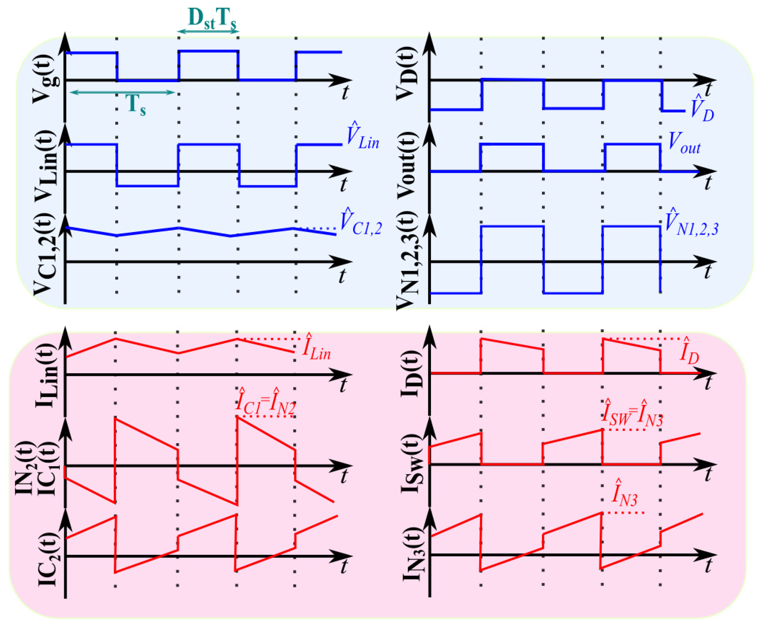
The QSY network comprises the diode D; the inductor L i n , which allows for the continuous current at the input stage; and the capacitor C 2 , which avoids core saturation due to the DC current component. Additionally, there are three coupled inductors N 1 : N 2 : N 3 , which, together with the capacitor C 1 , store energy during the converter operation. The power switch S w can represent a transistor bridge (half or full bridge configurations) in the case of DC-AC converters. The load impedance comprises R o and L o , respectively. A QSY impedance-source converter, operating in continuous conduction mode (CCM) and with tight magnetic coupling, has two main states of operation, namely, shoot-through and active states. The characteristic voltage and current waveforms are shown in Figure 2, where D s t and T s are the shoot-through duty cycle and switching period, respectively, and V g is the gate signal for S w , which is high at shoot-through periods and low during the active state.
The converter equivalent circuits for each state are depicted in Figure 3. During the shoot-through conduction state (in which S w is turned on and D is blocked), input energy is stored in the coupled inductors N 1 : N 2 : N 3 and C 1 is discharged, while the load current does not depend on the input stage. In the active state (in which D is turned on and S w is turned off), C 1 is charged and the energy coming from V i n is delivered to the load through diode D, together with the previously stored energy in the coupled inductors through DC-link coupling. Finally, the ideal voltage gain B = V o u t V i n of the QSY converter is given by B = 1 ( 1 δ D s t ) , where δ = N 1 + N 2 N 2 N 3 and D s t = 1 δ ( 1 B 1 ) represent the shoot-through duty-cycle. Moreover, auxiliary variable definitions are given as δ = 1 δ , D s t = 1 D s t .

2.2. Impedance Network Elements Design

For the steady-state analysis, the following assumptions are considered: (a) the coupled inductors leakage inductances are negligible due to a tight magnetic coupling; (b) the power switches S w and D have an instantaneous switching period; (c) the converter operates in CCM; (d) all of the passive elements are linear, time-invariant, and frequency independent. Moreover, considering the waveforms depicted in Figure 2 and the equivalent circuits during shoot-through and active states given in Figure 3, expressions of design interest can be derived for the components of the QSY network. Table 1 presents a summary of the obtained expressions. For DC-AC applications and SPWM-based control techniques, such as simple boost control [8], the shoot-through frequency may be defined as f s t = 2 f s , where f s may be the SPWM triangular wave carrier frequency.

2.2.1. Derivation of V C 1 and V C 2

Prior to obtaining the equations of the QSY network, expressions for V C 1 and V C 2 need to be obtained, considering that the voltage drop on the equivalent series resistances can be neglected on the steady state under voltage compensation control scheme. Applying Kirchhoff’s Voltage Law (KVL) on the circuit depicted in Figure 3a, the expression for N 1 winding voltage in the shoot-through state V N 1 . s t can be approximated as (1). In the same way, but considering the circuit shown in Figure 3b, the N 1 voltage in the active state V N 1 . a can be written as (2). Now, considering the Volt.s balance in the winding N 1 , an expression for the average voltage V N 1 ¯ can be written as (3). Hence, by substituting (1) and (2) for (3) one can derive (4), which expresses the relationship between V C 1 and V C 2 .
V N 1 . s t = V C 1 N 1 N 3 N 2
V N 1 . a = V C 2 N 1 N 1 + N 3
V N 1 ¯ = V N 1 . s t D s t T s + V N 1 . a ( 1 D s t ) T s T s = 0
V C 2 V C 1 = N 1 + N 3 N 2 N 3 D s t 1 D s t
However, both in the active and in the shoot-through state, by applying KVL on the input stage loop, one can obtain (5). The average expression of (5) can be given by (6), which reveals the relationship between the averaged values of V C 1 ( t ) and V C 2 ( t ) , which are very similar to its instantaneous values due to the low voltage ripple content.
V i n V L i n + V C 2 V N 1 N 1 + N 2 N 1 V C 1 = 0
V C 2 = V C 1 V i n
Finally, by substituting (6) for (4), the equations for V C 1 and V C 2 can be obtained by (7) and (8).
V C 1 = V i n ( 1 D s t ) 1 D s t δ
V C 2 = V i n D s t | δ | 1 D s t δ

2.2.2. Derivation of L i n

The V L i n expression can be written as (9). In steady state, during the shoot-through period and considering the waveform of i L i n ( t ) shown in Figure 2, d i L i n d t can be written as (10), where i L i n m i n is the minimum value of i L i n ( t ) .
V L i n = L i n d i L i n d t
d i L i n d t = Δ i L i n Δ t = i ^ L i n i L i n m i n D s t T s
For simplicity, considering a large enough inductance, Δ i L i n can be defined as a fraction of the average value of the input current i L i n ¯ , through the use of a current ripple factor k L i n , hence Δ i L i n = k L i n i L i n ¯ , where i L i n ¯ = P o V i n , with P o being the converter output power, neglecting power loss in the converter. Therefore, considering the previous comments, one can obtain (11). Now, by substituting (7), (8), and (1) for (5), the L i n voltage during shoot-through V L i n . s t can be given by (12). Finally, applying (11) and (12) in (9) L i n can be obtained as (13), where f s t is the shoot-through frequency.
Δ i L i n Δ t = i L i n ¯ k L i n D s t T s = P o k L i n V i n D s t T s
V L i n . s t = V i n ( 1 B δ )
L i n = V i n 2 ( 1 B δ ) D s t f s t P o k L i n

2.2.3. Derivation of L m

Considering that the coupled-inductor core can be treated as a uniform magnetic circuit, that is, the air-gap reluctance is incorporated in the core body, the expression of the equivalent reluctance R is given by (14), where l is the mean length of the magnetic circuit; μ o is the air magnetic permeability; μ r is the relative magnetic material permeability; and A is the core cross-section area. Now, based on the work developed by [37], the magnetizing inductance L m can be given by (15) and is related to core’s reluctance R and the number of windings N 1 , which is the coupled-inductor energy input coil.
R = l μ o μ r A
L m = N 1 2 R = N 1 2 μ o μ r A l

2.2.4. Derivation of C 2

The current and voltage associated with C 2 are related by (16), considering the shoot-through state and using the same methodology adopted in the L i n design, such that d V C 2 d t Δ V C 2 D s t T s and Δ V C 2 = k C 2 V C 2 . However, during the shoot-through state, i C 2 = i L i n , as can be inferred by the circuit shown on Figure 3a. Assuming that i L i n i L i n ¯ P o V i n , isolating C 2 in (16) and considering (8), one can obtain (17).
i C 2 = C 2 d V C 2 d t = C 2 k C 2 V C 2 D s t T s
C 2 = P o f s t k C 2 V o u t | δ | V i n

2.2.5. Derivation of C 1

The current and voltage association with C 1 , given by (18), is similar to (16), considering the shoot-through state and using the same methodology adopted in the L i n design, such that d V C 1 d t Δ V C 1 D s t T s and Δ V C 1 = k C 1 V C 1 . Now, as reported in [31], the windings and currents of each coupled-inductor coil are related by (19). Applying KCL on the coupled-inductors, one can derive (20). Despite the fact that I C 2 = I N 1 + i m , considering a large enough magnetizing inductance L m , i m is comparatively lower than I N 1 in steady state and hence during shoot-through I C 2 I N 1 . Therefore, by substituting (18) for (20), it is possible to derive expressions for I N 3 and I N 2 with respect to I N 1 and I C 2 , as can be seen in (20) and (21).
i C 1 = C 1 d V C 1 d t = C 1 k C 1 V C 1 D s t T s
N 1 I N 1 = N 2 I N 2 N 3 I N 3
I N 2 = I N 3 I N 1
I N 3 = I N 1 δ I C 2 δ
I N 2 = I N 1 | δ | I C 2 | δ |
Since i C 1 = I N 2 , then by isolating C 1 in (18) and considering (7), it is possible to obtain (23).
C 1 = | δ | D s t P o V o u t D s t f s t k C 1 V i n

2.2.6. Determination of R o and L o

The determination of R o , which is used to represent the load connected at the inverter output in the equivalent circuits depicted in Figure 3, is based on the AC load power consumption P o ; the value of the RMS DC-link voltage V o u t r m s ; and D s t . Hence, R o is derived by the authors of (24). On the other hand, if the inverter has output filter inductances, L o has the same value of such filter inductances.
R o = V o u t r m s 2 P o = V o u t 2 ( 1 D s t ) P o

2.3. Electrical Quantities Expressions for the QSY Converter

Through the analytical description of the characteristic waveforms depicted in Figure 2, and by applying Kirchhoff voltage (KVL) and current (KCL) laws to the equivalent circuits depicted in Figure 3, considering the inductor voltage and capacitor charge balance, the main voltage and current expressions for the QSY network are derived and shown in Table 2. For a generic quantity x, its RMS value is identified as x r m s , and its mean and peak values by x ¯ and x ^ , respectively. It can be noticed that the following parameters are needed to describe all of the voltage and current waveforms of the QSY inverter: (a) I L i n ¯ ; (b) k L i n , k C 1 , k C 2 ; (c) P o , V i n , η ; (d) B , D s t , δ ; (e) σ ; and (f) N 1 : N 2 : N 3 . It should be noted that the estimated converter efficiency, for a conservative design, should be adopted as 0.8 η 0.95 . The auxiliary design factor σ is used to approximate the derived results to more realistic scenarios, considering the converter’s non-ideal behavior, and is recommended to adopt σ = 1.1.

3. Small-Signal Model Derivation and Analysis

To describe the dynamics of the QSY converter, considering small deviations from a known operational point and control design, a small-signal model must be derived. In this paper, the “State-Space Averaging” technique [38] is used to derive the small-signal model of the QSY converter. The same assumptions adopted for the steady-state analysis are considered for obtaining the small-signal model. Moreover, in the following subsections, the state-space model and its validation, through computational simulations, are presented. It is worth mentioning that the derived dynamic model is valid for the QSY impedance network, hence the obtained transfer functions can be used to design controllers for different types of power converters applications, including DC-AC.

3.1. State-Space Model

The QSY converter operational states can be mathematically represented in the state-space format. Applying KVL and KCL to the equivalent circuit of shoot-through state, as depicted in Figure 3a, expressions (25)–(27) are derived.
V i n V L i n V r L i n V r C 2 V r N 1 + V C 2 V N 1 N 1 + N 2 N 1 V r C 1 V r N 2 V C 1 = 0
V C 1 + V r C 1 + V r N 2 + V N 1 N 2 N 3 N 1 V r S V r N 3 = 0
i L i n = i C 1 + i N 3 = i N 1 + i m
By isolating the state variables derivatives in (25)–(27), one can obtain (28)–(33), where γ 1 = δ r N 3 + r S , γ 2 = N 1 r N 3 + r S N 2 N 3 , and the λ factors, present in (28)–(46), are given in Appendix A.
d i L i n d t = V i n L i n + i L i n λ 1 + i m λ 2 + V C 1 λ 3 + V C 2 λ 4
d i o d t = 0
d i m d t = i L i n λ 5 + i m λ 6 + V C 1 λ 7
d V C 1 d t = i L i n λ 8 + i m λ 9
d V C 2 d t = i L i n λ 10
V o u t = i L i n γ 1 + i m γ 2
Similarly, but now considering the active state, it is possible to obtain (34)–(40) by applying KVL and KCL on the circuit of Figure 3b.
V i n V L i n V r L i n + V C 2 + V r C 2 V N 1 N 1 + N 2 N 1 V r C 1 V C 1 = 0
V C 1 + V r C 1 + V N 1 ( N 2 N 3 N 1 ) V r N 3 V R o V L o = 0
V C 2 + V r C 2 V N 1 N 1 + N 3 N 1 V r N 3 + V r D = 0
V i n V L i n V r L i n V D V R o V L o = 0
I L i n = I D I C 2
I C 2 = I N 1 I m = I C 1 I N 3
I N 3 + I D = I o
By isolating the state variables derivatives in (34)–(40), one can obtain (41)–(46), where γ 3 = ( r D δ + r N 1 + r C 2 ) δ 2 + r N 2 + δ δ 2 r N 3 + r C 1 , γ 4 = ( r D + r N 1 + r C 2 ) δ 2 r N 2 + δ δ 2 r N 3 r C 1 , γ 5 = N 1 ( r D + r N 1 + r C 2 ) δ ( N 1 + N 3 ) N 1 N 1 + N 2 N 1 + N 3 2 r N 3 , and γ 6 = 1 δ .
d i L i n d t = V i n L i n + i L i n λ 11 + i o λ 12 + i m λ 13 + V C 1 λ 14 + V C 2 λ 15
d i o d t = i L i n λ 16 + i o λ 17 + i m λ 18 + V C 1 λ 19 + V C 2 λ 20
d i m d t = i L i n λ 21 + i o λ 22 + i m λ 23 + V C 2 λ 24
d V C 1 d t = i L i n λ 25 + i o λ 26
d V C 2 d t = i L i n λ 27 + i o λ 28 + i m λ 29
V o u t = V C 1 + i L i n γ 3 + i o γ 4 + i m γ 5 + V C 2 γ 6
Therefore, managing the state variables definitions for active and shoot-through states, given by (28)–(46), in the matrix format, as indicated by (47)–(48), where n = 1 refers to shoot-through and n = 2 to the active state, one can obtain the matrices A 1 , A 2 , C 1 , C 2 , given by (49)–(51). Additionally, E 1 = E 2 = 0 and B 1 = B 2 = 1 L i n 0 0 0 0 T .
d x ( t ) d t = A n x ( t ) + B n u ( t )
y ( t ) = C n x ( t ) + E n u ( t )
A 1 = λ 1 0 λ 2 λ 3 λ 4 0 0 0 0 0 λ 5 0 λ 6 λ 7 0 λ 8 0 λ 9 0 0 λ 10 0 0 0 0 ; A 2 = λ 11 λ 12 λ 13 λ 14 λ 15 λ 16 λ 17 λ 18 λ 19 λ 20 λ 21 λ 22 λ 23 0 λ 24 λ 25 λ 26 0 0 0 λ 27 λ 28 λ 29 0 0
C 1 = γ 1 0 γ 2 0 0
C 2 = γ 3 γ 4 γ 5 1 γ 6
Yet, the state matrices are described by the vector x = [ i L i n , i o , i m , V C 1 , V C 2 ] T , and the input and output variables by U = V i n and y = V o u t , respectively. Through the definitions of matrices A n , B n , C n and E n for n = 1 and n = 2, it is possible to define the average matrices A avg , B avg , C avg , E avg , given by (52)–(55), respectively. Moreover, B d and E d matrices are defined by (56)–(57), where X is the DC terms matrix of state variables, given by (58). Finally, the output average value Y is given by (59).
A avg = A 1 D s t + A 2 D s t
B avg = B 1 D s t + B 2 D s t
C avg = C 1 D s t + C 2 D s t
E avg = E 1 D s t + E 2 D s t
B d = ( A 1 A 2 ) X + ( B 1 B 2 ) U
E d = ( C 1 C 2 ) X + ( E 1 E 2 ) U
X = A avg 1 B avg U
Y = ( C avg A avg 1 B avg + E avg ) U
The transfer functions considering the state variables in relation to the control and the input are given by (60) and (61), respectively, and the output variable to the input and control, by (62) and (63), respectively.
x ^ ( s ) d ^ ( s ) = ( s I A avg ) 1 B d
x ^ ( s ) u ^ ( s ) = ( s I A avg ) 1 B avg
y ^ ( s ) d ^ ( s ) = C avg ( s I A avg ) 1 B d + E d
y ^ ( s ) u ^ ( s ) = C avg ( s I A avg ) 1 B avg + E avg

3.2. Small-Signal Model Validation

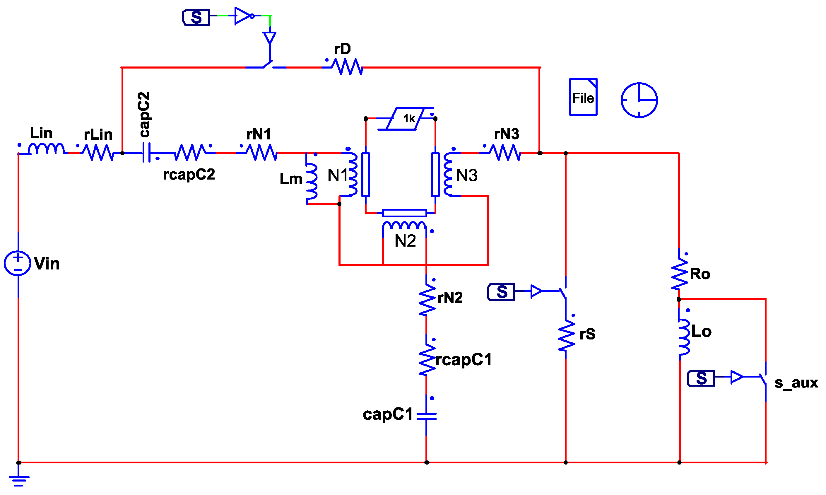
To evaluate the usefulness of the transfer functions obtained from the small-signal model, the QSY inverter equivalent circuit, depicted in Figure 3, was simulated using a switched circuit and the transfer functions, using PSIM and considering the parameters given in Table 3. The implemented circuit model on PSIM can be seen in Figure 4. The transient behaviors of the state-space variables due to a step of 3% in D s t are shown in Figure 5, considering the results relative to all state-space variables transfer functions and the respective switched circuit waveform. It should be clarified that the insertion of s a u x free-wheel switch, which does not modify the converter dynamics and modeling, is needed to turn the circuit behavior at PSIM similar to what is considered during the small-signal model derivation since the current through I L o cannot be interrupted abruptly during the transition from active to shoot-through state—as is the case in the mathematical model. As can be seen, the obtained results show that there is a satisfactory match between the theoretical prediction provided by the dynamic model and the switched converter operation.

3.3. Parametric Variation Analysis

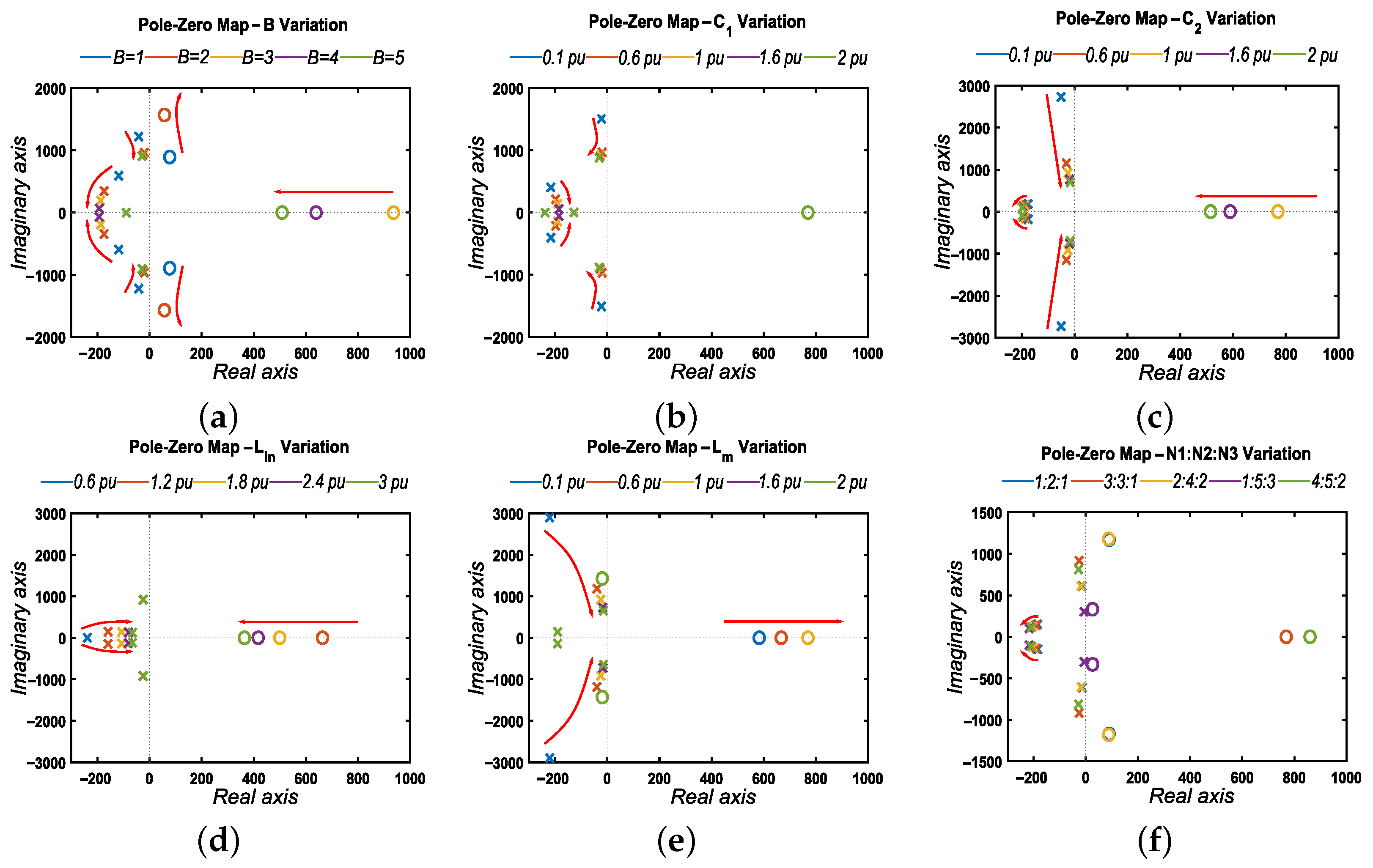
In this section, G V C 1 d ( s ) is going to be analyzed under a parametric variation on the QSY components since this transfer function is generally used to regulate V o u t , through indirect control [39]. The pole-zero maps for parametric variations carried out with different variables are depicted in Figure 6. Observations for each component variation are presented in the next subsections, with the aim of serving as guidelines to help specify the components of the QSY network for V o u t voltage regulation design requirements. Whenever indicated, 1 p.u stands for the base value of the relative component value shown in Table 3.

3.3.1. C 1

Higher C 1 values provide a more damped V o u t response with lower ringing content, which is a convenient characteristic for establishing a stable DC link. Furthermore, as can be seen in Figure 6b, there is no significant change in the position of the right half-plane zero (RHPZ) as C 1 increases, and the dominant complex pole-pairs tend to move away from the imaginary axis . There is an increase in the control bandwidth for the establishment of closed-loop control, as can be seen in Figure 7a. Considering the non-ideal scenarios, higher ESR values for C 1 help to obtain a more damped response and a slight increase in the non-minimum phase effect, which do not affect substantially the control bandwidth. Therefore, considering all of these aspects, it is recommended to adopt a k C 1 0.1 % when designing C 1 .

3.3.2. C 2

As C 2 is in series with the magnetizing branch, the higher values of C 2 tend to constrain energy storage on the magnetic core. Consequently, longer charging and recharging times are required for C 1 , which explains why a greater oscillatory V o u t response is observed when C 2 increases, as can be inferred by the approximation of the dominant complex poles to the origin in Figure 6c. From the control point of view, the determination of C 2 was the most impacting factor for the definition of the control bandwidth, and the control response speed increases significantly using lower values of C 2 , as can be seen in Figure 7a. As for the ESR characteristic of C 2 , it can be noticed that higher ESR values bring both the dominant complex poles and the RHPZ closer to the origin, which reduces control bandwidth. Hence, when designing C 2 , it is recommended to adopt k C 2 5 % .

3.3.3. L m

The increase in L m is associated either with greater values of μ r or a greater number of primary turns of the coupled inductors N 1 . For the case of higher values of μ r , the coupled inductors more likely behave as a transformer, storing less energy on the magnetic core. In this context, similarly to what happened when C 2 increased, the capacitor C 1 becomes insufficiently charged as μ r (or L m ) increases, which explains the increased ringing response of V o u t , as evidenced by approximation of the dominant poles to the origin, as can be seen on Figure 6e. However, the higher values of L m make the RHPZ move away from the origin, and besides the consequent phase gain increment for the medium frequencies range due to this RHPZ distancing, greater control bandwidth restrictions are observed due to the approximation of the dominant poles to the origin, which restricts stability margins. Hence, for the QSY converter, magnetic cores with lower L m are recommended either with (a) lower μ r , choosing cores based on sendust alloys or iron powder materials, for example, due to its characteristics of energy accumulation and greater control bandwidth for the V o u t control, as shown in Figure 7a; or (b) a lower number of windings in N 1 .

3.3.4. L i n

Greater values for L i n and consequently in its ESR cause a more damped response in the V o u t response and a decrease in i L i n ripple. However, changes in L i n values do not significantly affect the closed-loop control bandwidth because although the RHPZ approaches the origin, the dominant complex poles do not change its root loci significantly, which contributes to the fact that there is no expressive reduction in the system stability margins. Yet, it is emphasized that L i n must be large enough to avoid discontinuous conduction since the conclusions of this work do not apply to this scenario. Therefore, considering CCM, even in scenarios of load transients, it is recommended to adopt k L i n 50 % .

3.3.5. B, δ , D s t

Obtaining higher voltage gain B, with a fixed δ and increasing D s t , does not substantially change the V o u t transient response but may decrease the control-bandwidth due to the approximation of the RHPZ and dominant complex poles to the origin, as can be seen on Figure 6a. Additionally, as a result of the presence of ESR in several components of the QSY network, the B range is limited, as can be seen in Figure 7b. Therefore, if higher B voltage gains are desired, it is recommended to choose lower δ values, but greater shoot-through periods are observed, which increases switching and conduction losses. On the other hand, higher values of δ are indicated if the goal is to decrease switching losses while achieving relatively moderate B values. In any case, larger δ values imply a larger number of winding turns on the coupled inductors, which can result in greater voltage efforts in each coil and smaller and unpractical shoot-through periods, which may be incompatible with the semiconductor technology used in the power switches, due to the inherent delays involved in its switching process.

3.3.6. Coupled Inductor Winding Turns Ratio ( N 1 : N 2 : N 3 )

For the determination of the same δ , different winding proportions of N 1 : N 2 : N 3 can be used, which can modify the dynamic behavior of V o u t . In general, the choices of winding proportions that result in the presence of complex zeros or complex poles closer to the origin tend to present a lower control bandwidth, with narrower stability margins. This can be seen by contrasting the pole-zero maps of the 1:5:3 and 3:3:1 windings configurations, as shown in Figure 6f. For the 3:3:1 case, the control bandwidth is greater because both the complex poles and real RHPZ are far away from the origin and there is no complex RHPZ when compared to the 1:5:3 case. In this sense, once the δ is determined, it is recommended to choose N 1 : N 2 : N 3 configurations that show, in the G V C 1 d ( s ) , (a) no complex zeros and (b) dominant complex poles and real RHPZ as far away as possible from the origin.

4. Closed-Loop V o u t Voltage Controller Design

Referring to the steady-state operation of the QSY converter, it can be noticed that the DC link voltage can be regulated through C 1 voltage. Thus, a type II PI controller can be designed to indirectly regulate V o u t by controlling V C 1 , according to the strategy defined in [36]. In this sense, to demonstrate the usefulness of the proposed small-signal model, a close-loop DC-link voltage controller is designed for a three-phase/three-wire inverter, based on the transfer functions obtained through the dynamic model.
Figure 8 shows the power converter and control structure, and Figure 9 shows the built laboratory prototype. Considering the impedance network specifications given in Table 3, the compensated open-loop transfer function T c ( s ) in the continuous domain is defined as (64). To accommodate the shoot-through gate signals together with the sinusoidal PWM (SPWM), the simple boost control strategy was used based on the strategy given in [36], with the aid of an external digital circuit based on OR logic. The modulation strategy is based on a triangular carrier, with a peak value of 1, then P W M ( s ) = 1. Moreover, since C f behaves as a high impedance path to the inverter fundamental frequency current component, it can be neglected from the dynamic model. The voltage measurement feedback path H ( s ) comprises a voltage transducer, signal conditioning, and an analog-to-digital converter (A/D). Once the voltage signal V C 1 ( k ) is acknowledged by the DSP, a calibration gain k is applied such that the final reading value of V C 1 ( k ) is equal to V C 1 ( t ) , hence H ( s ) = 1 . The V C 1 to control transfer function G V C 1 d ( s ) is defined as (65).
T c ( s ) = G c v ( s ) P W M ( s ) G V C 1 d ( s ) H ( s )
G V C 1 d ( s ) = 0 0 0 1 0 ( s I A avg ) 1 B d
Before designing the controller ( G c v ( s ) = 1), the bode plot of the uncompensated open-loop T ( s ) is depicted in Figure 10. As can be seen, T ( s ) has a negative phase and gain margins, which means that the uncompensated system is naturally unstable, requiring the design of an adequate controller. Moreover, the presence of a non-minimum phase makes the controller design process more challenging since it is difficult to obtain a wider controller bandwidth as a wide phase addition is required at high frequencies. Finally, at lower frequencies, the gain is limited, which is not a desired feature in a voltage regulation application. Yet, it is desired that the voltage controller G c v has a quick response in the voltage reference following. Therefore, higher control bandwidth frequencies f b w are required. However, for non-minimum phase systems, as is the case for the QSY converter according to the small-signal analysis conducted earlier, it is not always possible to achieve higher values of f b w without having closed-loop instability. Therefore, taking these factors into consideration, the highest f b w value was set at f b w = 10 Hz. Higher values of phase margin P M exhibit a more damped response with a higher settling period. Lower values imply a lower settling time, but with converter responses that contain overshoot and ringing responses. Hence, P M = 70° was chosen as it presents a satisfactory compromise between response speed with more damped behavior. With all of these details defined, following the methodology described in [40], a type II PI controller in the continuous time domain was designed, with the expression given by (66). The bode plots of the controller G c v ( s ) and the compensated open-loop T c ( s ) are depicted in Figure 10. To obtain the digital controller, given by (67), a continuous to discrete bilinear transformation with a sampling frequency of 18 kHz was used. The coefficients of the digital controller are given in Table 4.
G c v ( s ) = 0.037461 ( s + 49.41 ) s ( s + 79.91 )
G c v ( z ) = b 0 + b 1 z 1 + b 2 z 2 a 0 + a 1 z 1 + a 2 z 2

5. Experimental and Simulation Results

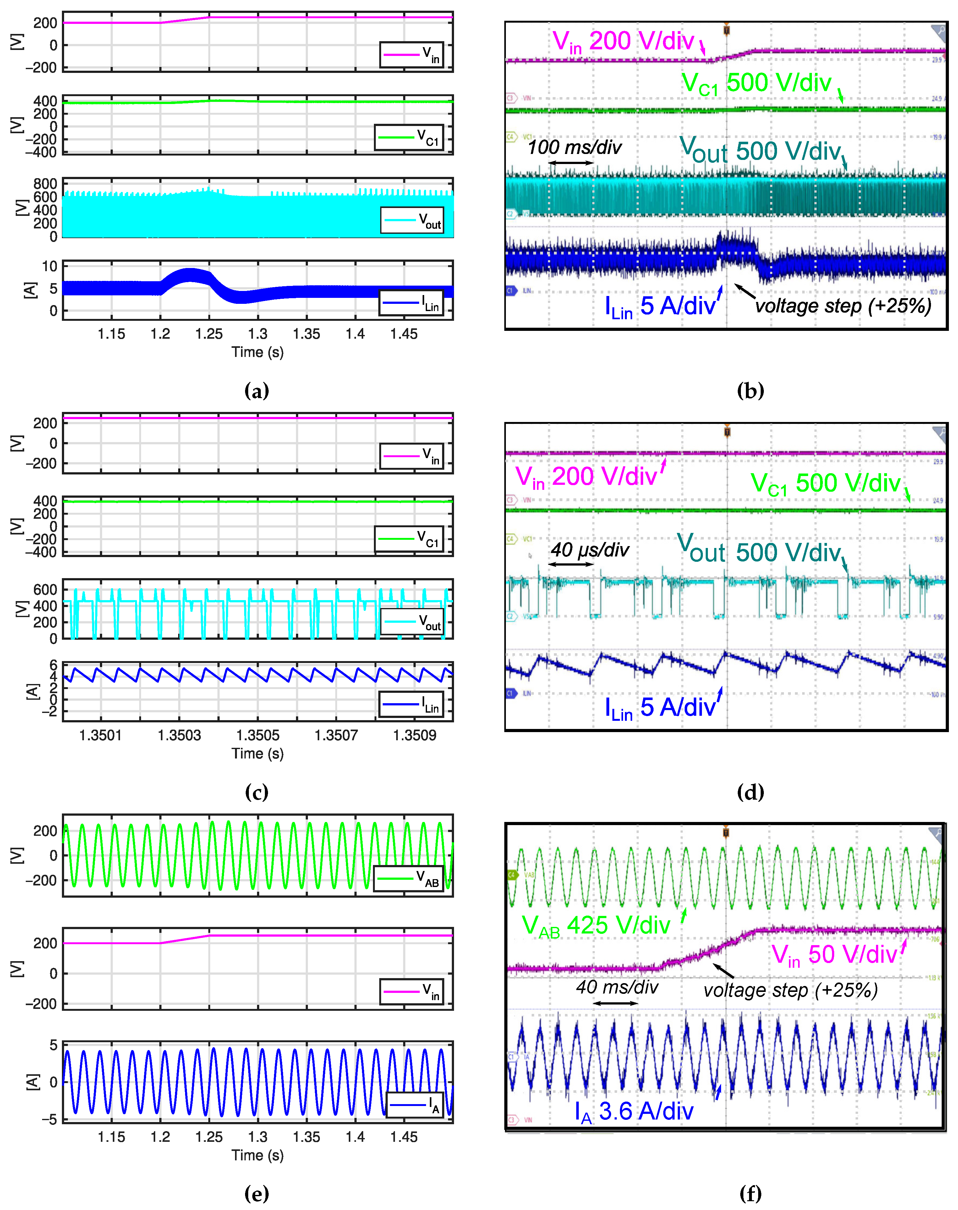
To verify the dynamic performance of the QSY converter and the adherence to the small-signal model, simulation and experimental tests were conducted considering the load transient and input voltage ramp variation. The V o u t voltage reference value was set to be regulated at 470 V, and Figure 11 and Figure 12 show the obtained results for both perturbations.

5.1. Simulation Considerations and Prototype Specifications

The same parameters shown in Table 3 were employed in the computer simulation using PSIM, with F28379D blocks for ADC and PWM peripherals configuration, and the SimCoder package for automatic code generation. The code generator tool from PSIM was used to create the controller C code, whereas Code Composer studio was used to upload the code to DSP F28379D. In the prototype shown in Figure 9, the coupled inductors were built on a toroidal core of sendust ( μ r = 60 H/m) with a winding turns ratio of 37:112:186, and 2x22 AWG and 3x20 AWG Litz wires. The capacitors C 1 and C 2 are implemented with the A511EJ68M450F and the 15 μ F, 500 V film capacitor model C4AQLLU5150A19K. The IRG4PF50WD IGBT and GC2X5MPS12 26 A and 1200 V SiC Schottky diode were used as S 1 6 and D. Furthermore, to relieve voltage spikes at the DC link, the LCD snubber was implemented with L s = 235 μ H, C s = 1.05 μ F, and RHRG30120 diode, based on the work developed in [41]. In the same way, an RC snubber was used in parallel with D with a resistance value of 270 Ω and a capacitance of 4 nF, with a design methodology inspired in [42].

5.2. Experimental and Simulation Results Analysis

In Figure 11b in the experimental test with constant input voltage V i n = 250 V and a load step resistance increase of 50%, it can be observed that before and after the load step, V o u t remains regulated at 470 V, as desired. As can be seen, the transient dynamics are overdamped with a settling time greater than 80 ms. This was expected due to the voltage control loop bandwidth set at 10 Hz and phase margin defined at 70 , which configure a slow dynamic response to the voltage regulation controller. As shown in Figure 11f, as V A B is directly related to V o u t , V A B also remains regulated, before and after the load transient. In Figure 11d, which shows the QSY converter waveforms for steady-state operation, after the load transient, it is verified that V o u t remains at the desired voltage level (470 V) and stable, with minimum steady-state error. Now, considering the input voltage variation, as shown in Figure 12b, the converter load remains constant, and there is an input voltage ramp variation from 200 V to 250 V (25% increase); the V o u t voltage remains regulated at 470 V, with a similar dynamic characteristic present in the input voltage variation test. As depicted in Figure 12f, V A B remains constant before and after the input voltage variation. In Figure 12d, which shows the converter waveforms for steady-state operation after the input voltage variation, it can be observed that V o u t remains regulated at 470 V. In general, both in the cases of load transient or input voltage ramp variation, it can be noticed that the controller action compensates the V o u t disturbances in an adequate manner, maintaining the voltage level at the desired values, which consequently validates the dynamic model used to design the controller. This is also confirmed by comparing the computational simulations, both for the case of load transition (Figure 11a,c,e) or input voltage variation (Figure 12a,c,e), with the experimental results, as the simulation results represent the results observed in the experimental tests very well, particularly for the controller dynamics, which again confirms the validity of the dynamic model developed.

6. Conclusions

In this paper, a comprehensive analysis of the QSY converter was carried out, including a complete steady-state analysis, component-specification equations, small-signal model proposition, and converter components’ parametric variation impact on dynamic behavior and control design. To confirm the validity of the proposed dynamic model, a type-II PI controller was designed, using the transfer functions obtained by the small-signal model, using both computer simulations and experimental tests. The obtained results show that the proposed dynamic model represents the behavior of a real QSY converter with adequate fidelity. Moreover, with the indications given for the converter components design, including expressions for the determination of L i n , L m , C 1 , and C 2 and several converter currents and voltages RMS, peak, and average values, one can obtain a starting point for determining the converter project. Additionally, with the evaluation of each component parametric variation, it is possible to obtain a clear outlook of each converter component selection, aiming at DC-link voltage regulation applications, considering control design aspects and steady-state operation trade-offs for each case. All of these aspects were not treated in detail for any Y-source impedance source network in the current literature and promote the consolidation of the Quasi-Y impedance-source inverter and its application in real renewable energy generation scenarios. Furthermore, the contributions given in this paper can also be used to implement more advanced control techniques with multiple feedback loops and can be extended to analyze other recently proposed Y-source-based impedance-source networks.

Author Contributions

Conceptualization, R.S.; methodology, R.S., F.A.S.G.; software, M.V.M.R.; validation, R.S., L.D.O.A.; formal analysis, R.S., F.A.S.G., L.D.O.A.; resources, F.A.S.G.; writing—R.S., draft preparation, R.S.; writing—review and editing, M.V.M.R., F.A.S.G., L.D.O.A.; supervision, F.A.S.G.; project administration, F.A.S.G.; and funding acquisition, F.A.S.G. All authors have read and agreed to the published version of the manuscript.

Funding

This research was funded by #2016/08645-9 and #2018/24331-0 grants, São Paulo Research Foundation (FAPESP), by #311331/2022-0 grant from the National Council for Scientific and Technological Development (CNPq), and in part by the Coordination for the Improvement of Higher Education Personnel (CAPES) under Finance Code 001.

Data Availability Statement

Not applicable.

Conflicts of Interest

The authors declare no conflict of interest. The funders had no role in the design of the study; in the collection, analyses, or interpretation of data; in the writing of the manuscript; or in the decision to publish the results.

Abbreviations

The following abbreviations are used in this manuscript:
V o u t  Quasi-Y-Source(QSY) peak DC-link voltage
V i n  QSY input voltage
D QSY network diode
r D D equivalent series resistance
L i n  QSY network input inductor
r L i n L i n equivalent series resistance
i L i n  QSY input current
L m  QSY magnetizing inductance
i m  QSY magnetizing current
C 1 , C 2  QSY network capacitors
r C 1 , r C 2 C 1 , C 2 equivalent series resistances
V C 1 , V C 2 C 1 and C 2 voltages
N 1 : N 2 : N 3  Coupled inductor winding turns ratio
δ  QSY network winding factor
δ  Defined as δ = 1 δ
S w  QSY network output power transistor
S 1 6  Three-phase bridge power transistors
r S S w equivalent series resistance
m a , b , c  DC-AC modulation index for phases A,B,C
V A B  DC-AC output line voltage
R o  Output load resistance
L o  Output load inductance
L f  Output inductor of DC-AC passive filter
C f  Output capacitor of DC-AC passive filter
i A , i B , i C  Phase currents of DC-AC converter
P o  Output load power
i o u t  Output load current
D s t  Shoot-through duty-cycle
D s t  Defined as D s t = 1 D s t
f s  Switching frequency
f s t  Shoot-through switching frequency
T s  Switching period
V g  Gate signal for S w
B QSY converter voltage gain
k L i n  Ripple factor for L i n
k C 1 , k C 2  Ripple factor for C 1 , C 2
μ o  Vacuum magnetic permeability
μ r  Relative magnetic permeability
A Coupled inductor core cross-section area
l Coupled inductor mean magnetic length
σ  Auxiliary design factor
η  Converter efficiency
A 1 , B 1 , C 1 , E 1  Shoot-through state matrices
A 2 , B 2 , C 2 , E 2  Active state matrices
λ 1 λ 29  Factors for A 1 and A 2 matrices
A avg E avg  State-space model average matrices
B d , E d  State-space model auxiliary matrices
X  State-space model DC terms matrix
Y  State-space model output DC term
G V C 1 d ( s ) C 1 Voltage to control transfer function
G c v ( s ) , G c v ( z )  Voltage controller transfer functions
T ( s )  Open-loop uncompensated transfer function
T c ( s )  Open-loop compensated transfer function

Appendix A

Appendix A.1. A1 and A2 Matrices λ Factors

λ 1 = r L i n + r N 1 + r C 2 + δ r N 2 + r C 1 + δ δ r N 3 + r S δ r N 2 + r C 1 L i n
λ 2 = N 1 δ r N 2 r C 1 r N 2 + δ r N 3 + δ r S + δ r C 1 L i n N 2 N 3
λ 3 = δ 1 L i n
λ 4 = 1 L i n
λ 5 = N 1 δ r N 3 + r S δ r N 2 + r C 1 L m N 2 N 3
λ 6 = N 1 2 r N 2 + r N 3 + r S + r C 1 L m N 2 N 3 2
λ 7 = N 1 L m N 2 N 3
λ 8 = δ C 1
λ 9 = N 1 C 1 N 2 N 3
λ 10 = 1 C 2
λ 11 = ( r N 1 + r C 2 ) L i n δ 2 r N 2 + r L i n + r C 1 L i n + N 1 + N 2 L i n δ N 1 + N 3 δ ( r D + r N 3 )
λ 12 = r N 1 + r C 2 L i n δ 2 + r N 2 + r C 1 L i n + N 1 + N 2 L i n δ N 1 + N 3 ( r N 3 δ + r D )
λ 13 = N 1 N 1 + N 2 N 1 + N 3 2 N 1 N 1 + N 3 ( r N 1 + r C 2 ) L i n + N 1 N 1 + N 2 N 1 + N 3 2 ( r N 3 + r D ) L i n
λ 14 = 1 L i n
λ 15 = N 2 N 3 L i n N 1 + N 3
λ 16 = ( r D δ + r N 1 + r C 2 ) L o δ 2 + r N 2 L o + N 1 + N 2 L o δ N 1 + N 3 r N 3 δ + r C 1 L o
λ 17 = ( r D + r N 1 + r C 2 ) L o δ 2 ( r N 2 + r C 1 + R o ) L o + N 1 + N 2 L o δ N 1 + N 3 r N 3 δ
λ 18 = N 1 N 1 + N 3 N 1 N 1 + N 2 N 1 + N 3 2 ( r D + r N 1 + r C 2 ) L o N 1 N 1 + N 2 N 1 + N 3 2 r N 3 L o
λ 19 = 1 L o
λ 20 = N 2 N 3 L o N 1 + N 3
λ 21 = N 1 ( δ ( r D + r N 3 ) + r N 1 + r C 2 ) L m δ N 1 + N 3
λ 22 = N 1 ( r D + r N 1 + r N 3 δ + r C 2 ) L m δ N 1 + N 3
λ 23 = N 1 2 ( r D + r N 1 + r N 3 + r C 2 ) L m N 1 + N 3 2
λ 24 = N 1 L m N 1 + N 3
λ 25 = 1 C 1
λ 26 = 1 C 1
λ 27 = 1 C 2 δ
λ 28 = 1 C 2 δ
λ 29 = N 1 C 2 N 1 + N 3

References

  1. Ibrahim, I.A.; Ötvös, T.; Gilmanova, A.; Rocca, E.; Ghanem, C.; Wanat, M. International Energy Agency; Kluwer Law International BV: Alphen aan den Rijn, The Netherlands, 2021. [Google Scholar]
  2. Andersen, G.K.; Klumpner, C.; Kjær, S.B.; Blaabjerg, F. A new power converter for fuel cells with high system efficiency. Int. J. Electron. 2003, 90, 737–750. [Google Scholar] [CrossRef]
  3. Baddipadiga, B.P.; Ferdowsi, M. A high-voltage-gain dc-dc converter based on modified dickson charge pump voltage multiplier. IEEE Trans. Power Electron. 2016, 32, 7707–7715. [Google Scholar] [CrossRef]
  4. Siwakoti, Y.P.; Loh, P.C.; Blaabjerg, F.; Town, G. Y-source impedance network. Trans. Power Electron. 2014, 29, 3250–3254. [Google Scholar] [CrossRef]
  5. Zeng, Z.; Yang, H.; Zhao, R.; Cheng, C. Topologies and control strategies of multi-functional grid-connected inverters for power quality enhancement: A comprehensive review. Renew. Sustain. Energy Rev. 2013, 24, 223–270. [Google Scholar] [CrossRef]
  6. Grgić, I.; Vukadinović, D.; Bašić, M.; Bubalo, M. Photovoltaic System with a Battery-Assisted Quasi-Z-Source Inverter: Improved Control System Design Based on a Novel Small-Signal Model. Energies 2022, 15, 850. [Google Scholar] [CrossRef]
  7. Monjo, L.; Sainz, L.; Mesas, J.J.; Pedra, J. Quasi-Z-source inverter-based photovoltaic power system modeling for grid stability studies. Energies 2021, 14, 508. [Google Scholar] [CrossRef]
  8. Peng, F.Z. Z-source inverter. IEEE Trans. Ind. Appl. 2003, 39, 504–510. [Google Scholar] [CrossRef]
  9. Siwakoti, Y.P.; Peng, F.Z.; Blaabjerg, F.; Loh, P.C.; Town, G.E. Impedance-source networks for electric power conversion part I: A topological review. IEEE Trans. Power Electron. 2014, 30, 699–716. [Google Scholar] [CrossRef]
  10. Zhu, M.; Yu, K.; Luo, F.L. Switched inductor Z-source inverter. IEEE Trans. Power Electron. 2010, 25, 2150–2158. [Google Scholar]
  11. Zhu, M.; Li, D.; Loh, P.C.; Blaabjerg, F. Tapped-inductor Z-source inverters with enhanced voltage boost inversion abilities. In Proceedings of the 2010 IEEE International Conference on Sustainable Energy Technologies (ICSET), Kandy, Sri Lanka, 6–9 December 2010; pp. 1–6. [Google Scholar]
  12. Li, D.; Gao, F.; Loh, P.C.; Zhu, M.; Blaabjerg, F. Hybrid-source impedance networks: Layouts and generalized cascading concepts. IEEE Trans. Power Electron. 2010, 26, 2028–2040. [Google Scholar] [CrossRef]
  13. Loh, P.C.; Blaabjerg, F. Magnetically coupled impedance-source inverters. IEEE Trans. Ind. Appl. 2013, 49, 2177–2187. [Google Scholar] [CrossRef]
  14. Rezazadeh, H.; Monfared, M.; Nikbahar, A.; Sharifi, S. A family of high voltage gain quasi-Δ-source impedance networks. IET Power Electron. 2021, 14, 807–820. [Google Scholar] [CrossRef]
  15. Reddivari, R.; Jena, D.; Gautham, T. Analysis, design, and performance evaluation of differential-mode Y-source converters for voltage spikes mitigation. IEEE Trans. Ind. Appl. 2020, 56, 6701–6710. [Google Scholar] [CrossRef]
  16. Zhou, M.; Liu, C.; Zhang, M.; Mao, X.; Zhang, Y. High Step-up Soft Switching DC-DC Converter Integrated with Y-Source Network. IEEE J. Emerg. Sel. Top. Power Electron. 2023, 11, 3348–3358. [Google Scholar] [CrossRef]
  17. Siwakoti, Y.P.; Loh, P.C.; Blaabjerg, F.; Andreasen, S.J.; Town, G.E. Y-source boost DC/DC converter for distributed generation. IEEE Trans. Ind. Electron. 2014, 62, 1059–1069. [Google Scholar] [CrossRef]
  18. Wang, W.; Wang, Y.; Guan, Y.; Yao, T.; Wang, Y.; Xu, D. A Family of Impedance Source DC-DC Converters With Zero Input Current Ripple. IEEE Trans. Ind. Electron. 2022, 70, 8883–8894. [Google Scholar] [CrossRef]
  19. Guan, Y.; Cheng, Y.; Yao, T.; Wang, Y.; Wang, W.; Xu, D. A High-Performance DC–DC Converter With Soft Switching Characteristic and High Voltage Gain. IEEE Trans. Power Electron. 2022, 37, 12279–12288. [Google Scholar] [CrossRef]
  20. Yao, T.; Guan, Y.; Cheng, Q.; Wang, Y.; Dalla Costa, M.A.; Alonso, M.; Xu, D.; Wang, W. High Performance Y-source Converters Based on Switched Inductor. In Proceedings of the 2022 IEEE Industry Applications Society Annual Meeting (IAS), Detroit, MI, USA, 9–14 October 2022; pp. 1–5. [Google Scholar]
  21. Nikbahar, A.; Monfared, M. Smooth DC-Link Y-source inverters: Suppression of Shoot-through current and avoiding DC magnetism. IEEE Trans. Power Electron. 2022, 37, 12357–12369. [Google Scholar] [CrossRef]
  22. Siwakoti, Y.P.; Loh, P.C.; Blaabjerg, F.; Town, G.E. Effects of leakage inductances on magnetically coupled Y-source network. IEEE Trans. Power Electron. 2014, 29, 5662–5666. [Google Scholar] [CrossRef]
  23. Yadav, A.; Chandra, S.; Bajaj, M.; Sharma, N.K.; Ahmed, E.M.; Kamel, S. A topological advancement review of magnetically coupled impedance source network configurations. Sustainability 2022, 14, 3123. [Google Scholar] [CrossRef]
  24. Reddivari, R.; Jena, D. A correlative investigation of impedance source networks: A comprehensive review. IETE Tech. Rev. 2022, 39, 506–539. [Google Scholar] [CrossRef]
  25. Rajaei, A.; Yazdani, S.; Ebadi, E. PMSG-Based Stand-alone Wind Energy Conversion System Using Quasi Y-Source Inverter and Battery Storage. In Proceedings of the 2022 13th Power Electronics, Drive Systems, and Technologies Conference (PEDSTC), Tehran, Iran, 1–3 February 2022; pp. 81–85. [Google Scholar]
  26. Reddivari, R.; Jena, D. Improved Gamma type Y-source inverter for rooftop PV based VG applications. Int. J. Electr. Power Energy Syst. 2022, 142, 108261. [Google Scholar] [CrossRef]
  27. Ismeil, M.A.; Orabi, M.; Abdelaal, O. High Robust Control Model of High Step Up Three Phase Y Source Inverters based on Model Predictive Control. SVU-Int. J. Eng. Sci. Appl. 2023, 4, 76–83. [Google Scholar] [CrossRef]
  28. Siwakoti, Y.P.; Blaabjerg, F.; Loh, P.C. Quasi-Y-Sourceboost DC–DC converter. IEEE Trans. Power Electron. 2015, 30, 6514–6519. [Google Scholar] [CrossRef]
  29. Siwakoti, Y.P.; Blaabjerg, F.; Loh, P.C. Quasi-Y-Sourceinverter. In Proceedings of the 2015 Australasian Universities Power Engineering Conference (AUPEC), Wollongong, Australia, 27–30 September 2015; pp. 1–5. [Google Scholar]
  30. Shafiei, S.; Mehdizadeh, A.; Khorsandi, A. AC Equivalent Circuit of Quasi Y-Source Converter Using by Averaged-Switch Model. In Proceedings of the 2022 13th Power Electronics, Drive Systems, and Technologies Conference (PEDSTC), Tehran, Iran, 1–3 February 2022; pp. 603–608. [Google Scholar]
  31. Forouzesh, M.; Siwakoti, Y.P.; Blaabjerg, F.; Hasanpour, S. Small-signal modeling and comprehensive analysis of magnetically coupled impedance-source converters. IEEE Trans. Power Electron. 2016, 31, 7621–7641. [Google Scholar] [CrossRef] [Green Version]
  32. Shehata, E.; Thomas, J.; Brisha, A.; Wageh, M. Design and analysis of a quasi y-source impedance network dc-dc converter. In Proceedings of the 2017 Nineteenth International Middle East Power Systems Conference (MEPCON), Cairo, Egypt, 19–21 December 2017; pp. 235–241. [Google Scholar]
  33. Ananth, D.; Chinna, D.S.; Sairam, G.; Naveen, M.; BhaskarRao, A.; Rao, B.J. Design and Analysis of High Gain Quasi Y-Source Impedance Network. Int. J. Sci. Res. Sci. Eng. Technol. 2020, 7, 1–7. [Google Scholar] [CrossRef]
  34. Abdelaal, O.; Ismeil, M.A.; Orabi, M. Model predicitve control of quasi y-source inverter. In Proceedings of the 2019 21st International Middle East Power Systems Conference (MEPCON), Cairo, Egypt, 17–19 December 2019; pp. 478–483. [Google Scholar]
  35. Fathima, K.; Vishnupriya, R.; Pavithra, M.; Devi, V.P. Improved DC bus voltage regulation for a DC distribution system using quasi Y source converter. In Proceedings of the 2017 International Conference on Power and Embedded Drive Control (ICPEDC), Chennai, India, 16–18 March 2017; pp. 446–452. [Google Scholar]
  36. Ding, X.; Qian, Z.; Yang, S.; Cui, B.; Peng, F. A PID control strategy for DC-link boost voltage in Z-source inverter. In Proceedings of the APEC 07-Twenty-Second Annual IEEE Applied Power Electronics Conference and Exposition, Anaheim, CA, USA, 25 February–1 March 2007; pp. 1145–1148. [Google Scholar]
  37. Witulski, A.F. Introduction to modeling of transformers and coupled inductors. IEEE Trans. Power Electron. 1995, 10, 349–357. [Google Scholar] [CrossRef]
  38. Middlebrook, R.D.; Cuk, S. A general unified approach to modelling switching-converter power stages. In Proceedings of the 1976 IEEE Power Electronics Specialists Conference, Cleveland, OH, USA, 8–10 June 1976; pp. 18–34. [Google Scholar]
  39. Siwakoti, Y.P.; Peng, F.Z.; Blaabjerg, F.; Loh, P.C.; Town, G.E.; Yang, S. Impedance-source networks for electric power conversion part II: Review of control and modulation techniques. IEEE Trans. Power Electron. 2014, 30, 1887–1906. [Google Scholar] [CrossRef]
  40. Venable, H.D. The K factor: A new mathematical tool for stability analysis and synthesis. In Proceedings of the Powercon, San Diego, CA, USA, 22–24 March 1983; Volume 10, pp. 1–12. [Google Scholar]
  41. Forouzesh, M.; Abdelhakim, A.; Siwakoti, Y.; Blaabjerg, F. Analysis and design of an energy regenerative snubber for magnetically coupled impedance source converters. In Proceedings of the 2018 IEEE Applied Power Electronics Conference and Exposition (APEC), San Antonio, TX, USA, 4–8 March 2018; pp. 2555–2561. [Google Scholar]
  42. Ridley, R. Flyback converter snubber design. Switch. Power Mag. 2005, 12, 1–7. [Google Scholar]
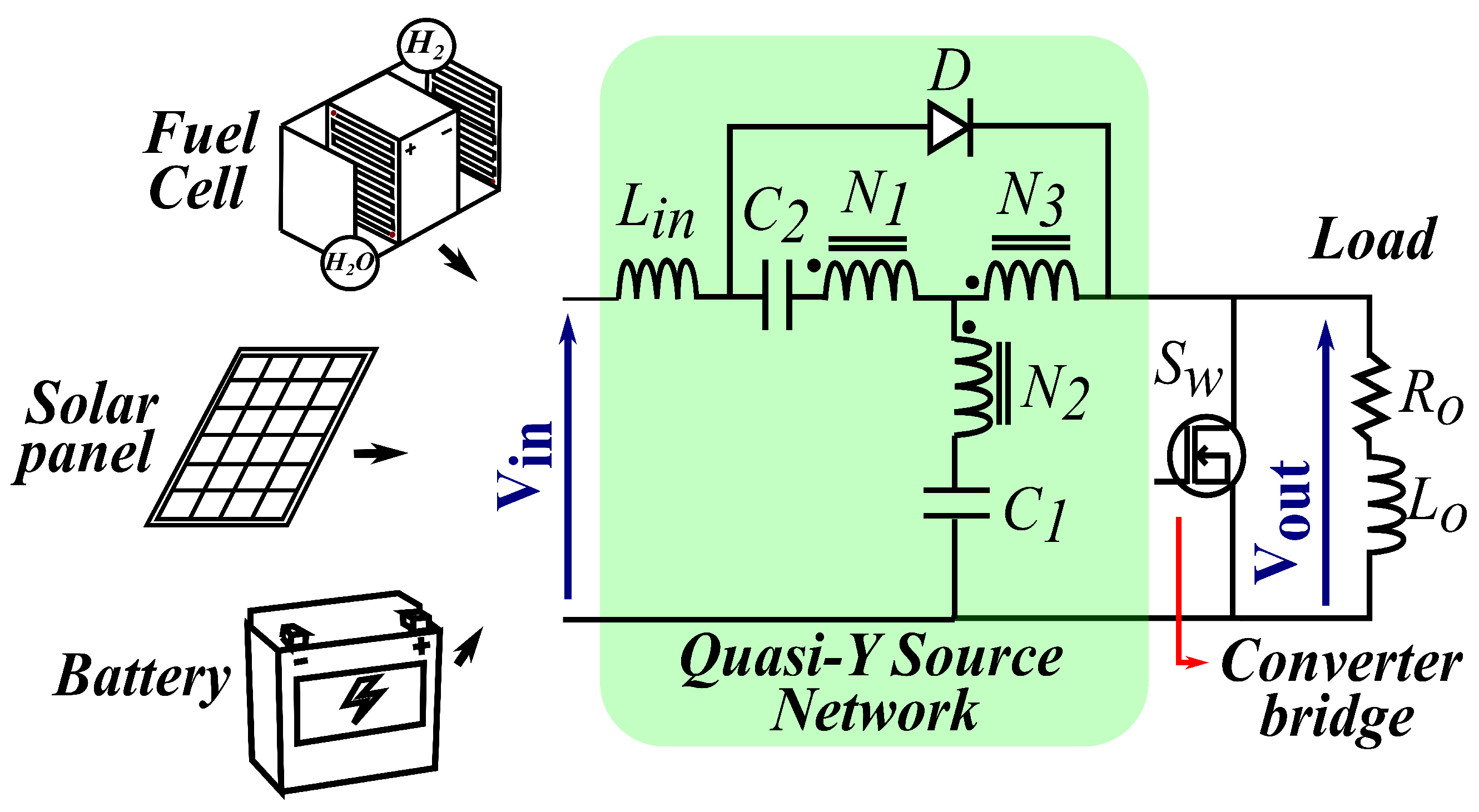
Figure 1. Equivalent circuit for the QSY inverter.
Energies 16 04877 g001
Figure 2. The characteristic voltage and current waveforms of the QSY converter.
Energies 16 04877 g002
Figure 3. Equivalent circuits of the QSY converter: (a) shoot–through state; (b) active state.
Energies 16 04877 g003
Figure 4. Equivalent QSY inverter circuit built on PSIM.
Energies 16 04877 g004
Figure 5. State-space variables for the switched circuit and small-signal transfer functions—waveforms comparison: (a) I L i n ( t ) , (b) I o ( t ) , (c) I m ( t ) , (d) V C 1 ( t ) , and (e) V C 2 ( t ) .
Energies 16 04877 g005
Figure 6. Pole-zero maps considering parametric variations for: (a) B; (b) C 1 ; (c) C 2 ; (d) L i n ; (e) L m ; (f) N 1 : N 2 : N 3 .
Energies 16 04877 g006
Figure 7. Components variation analysis: (a) control bandwidth for different components values; (b) non-ideal B ( δ , D s t ) .
Energies 16 04877 g007
Figure 8. QSY inverter and control structure.
Energies 16 04877 g008
Figure 9. QSY inverter developed prototype.
Energies 16 04877 g009
Figure 10. Bode plots of T ( s ) , T c ( s ) , and G c v ( s ) .
Energies 16 04877 g010
Figure 11. QSY converter waveforms for load transient : (1) Simulation: (a,c,e); (2) Experimental: (b,d,f).
Energies 16 04877 g011
Figure 12. QSY converter waveforms for input voltage ramp variation : (1) Simulation: (a,c,e); (2) Experimental: (b,d,f).
Energies 16 04877 g012
Table 1. Design expressions for the QSY impedance network components.
ComponentExpression
L i n V i n 2 ( 1 B δ ) D s t f s t P o k L i n
L m N 1 2 μ 0 μ r A l
C 1 | δ | D s t P o V o u t D s t f s t k C 1 V i n
C 2 P o V o u t | δ | f s t k C 2 V i n
R o V o u t 2 ( 1 D s t ) P o
Table 2. Set of expressions related to the main electrical quantities in the QSY converter.
VariableExpressionVariableExpression
I ^ L i n , I ^ C 2 I L i n ¯ ( 1 + k L i n 2 ) I N 1 r m s I C 2 r m s
I L i n ¯ P o V i n η V ^ C 1 V C 1 ¯ ( 1 + k C 1 2 )
I L i n r m s I L i n ¯ 1 + k L i n 2 12 V C 1 ¯ , V C 1 r m s V i n B D s t
V ^ L i n V i n ( B 1 ) D s t D s t I C 1 r m s I N 2 r m s
I N 1 , 2 , 3 ¯ 0 I D ^ I L i n ¯ σ 1 + k L i n 2 + 2 D s t D s t
I C 2 r m s I L i n ¯ D s t k L i n 2 D s t + 4 ( D s t + 3 ) 12 D s t D s t I D ¯ I L i n ¯
I ^ N 2 I L i n ^ | δ | σ I D r m s I L i n ¯ 2 3 16 D s t + ( k L i n 2 ) ( k L i n D s t + 2 ( D s t + 1 ) )
I N 2 r m s I C 2 r m s | δ | V D ^ V i n δ D s t δ D s t ( 1 + B ( δ D s t δ ) )
I ^ N 3 I L i n ^ δ σ I S w r m s I L i n ¯ δ k L i n D s t 3 σ 2 σ + 1 4 + σ 2 ( k L i n + 1 ) + σ k L i n + 1 k L i n 2
I N 3 r m s I C 2 r m s δ I S w ^ I ^ N 3
V ^ C 2 V C 2 ¯ ( 1 + k C 2 2 ) I S w ¯ I L i n ¯ D s t δ 4 ( σ ( 2 + k L i n ) + 2 k L i n )
V C 2 ¯ , V C 2 r m s V i n ( B D s t 1 ) V ^ S w V i n B
V ^ N 1 V i n N 1 N 1 + N 2 D s t ( 1 B ) D s t V ^ N 2 , V ^ N 3 N 2 N 1 V ^ N 1 , N 3 N 1 V ^ N 1
Table 3. QSY converter circuit parameters.
ComponentValueComponentValue
L i n 4.24 mH r L i n 0.85 Ω
C 2 15 μ F r C 2 29.33 m Ω
C 1 2040 μ F r C 1 142.68 m Ω
r D 25 m Ω r S 25 m Ω
L m 0.222 mH N 1 : N 2 : N 3 37:186:112
R o 149.27 Ω L o 10 mH
V i n 250 V f s t 18 kHz
δ 3.0135 D s t 155.328689 × 10 3
Table 4. Digital voltage controller coefficients.
CoefficientValueCoefficientValue
a 0 1 b 0 1.03971074368126 × 10 6
a 1 −1.99557051716865 b 1 2.84981554283603 × 10 9
a 2 9.95570517168651 × 10 1 b 2 −1.03686092813842 × 10 6
Disclaimer/Publisher’s Note: The statements, opinions and data contained in all publications are solely those of the individual author(s) and contributor(s) and not of MDPI and/or the editor(s). MDPI and/or the editor(s) disclaim responsibility for any injury to people or property resulting from any ideas, methods, instructions or products referred to in the content.