Article

Modelling of Bidirectional Three-Phase Four-Wire Three-Level NPC MLC under Single-Loop Current Sensorless Control

by
Alexander Suzdalenko
1,2,*,
Vsevolod Burenin
2,
Jaroslavs Zarembo
2 and
Janis Zakis
1,2
1
Institute of Industrial Electronics and Electrical Engineering, Riga Technical University, LV-1048 Riga, Latvia
2
JSC “Riga Electric Machine Building Works”, LV-1005 Riga, Latvia
*
Author to whom correspondence should be addressed.
Energies 2023, 16(12), 4599; https://doi.org/10.3390/en16124599
Submission received: 21 March 2023 / Revised: 4 June 2023 / Accepted: 6 June 2023 / Published: 8 June 2023

Abstract

:
Single-loop current sensorless control allows for abolishing of the instantaneous current measurement in the control system using only a single control loop with voltage feedback to stabilise the DC-bus voltage. This approach eliminates current sensors in the control circuit, benefiting from saving space on the printed circuit board and minimising power dissipation in the current measurement circuitry. This paper focuses on the single-loop current sensorless control applied to bidirectional three-phase four-wire three-level NPC MLC by simulation analysis and demonstrates the performance of the proposed current control algorithm in the rectifier and inverter modes and the step response with power direction change and grid-voltage change. In capacitor voltage balancing, an additional controller is applied, which is capable of compensating for the voltage asymmetry caused by adding a 2.5 kOhm resistor in parallel to one of the DC-bus capacitors. Our results demonstrate good performance of the proposed control method both in the inverter and rectifier modes, showing stable current shape in the low power and full power modes with acceptable harmonics content, meeting the requirements of the IEC 61000-3-2 standard for Class A devices. The analysis showed that the proposed control approach is suitable for industrial application.

1. Introduction

Developments in power electronics follow different directions. Novel ideas in material science provide for switching elements with close to ideal switch parameters. The module-type packaging allows designing of industrial types of converters based on various topologies packed in the module. Among those most frequently used in the industry are half-bridge and full-bridge topologies; however, module-type packaging for T-type, multilevel neutral-point clamped and matrix topologies that have appeared on the market are becoming the industry standard topology. Development of the module packaging allows for the use of most of the benefits of technologies such as SiC [1] and GaN [2] switches, resulting in higher efficiencies and more compact design of the end product.
Researchers are also focusing on new control approaches applied to the mitigating issues of the power electronics converters introduced by new applications of switching converters. The Green Deal or Energy Transition pushes industry to develop power converters with high reliability for such applications as e-mobility, photovoltaics, etc. For this reason, the converters should have redundancy to basic faults [3] or should be equipped with condition monitoring by using dedicated measurement circuitry and/or special data processing techniques to estimate degradation of the main components. The importance of device reliability in PELS converters is well discussed in [4], providing arguments in favour of condition monitoring and a review on corresponding techniques. Condition monitoring of MOSFET and the IGBT module based on a modified PWM strategy and measurement routine capable of detecting bond-wire lift-offs due to increased voltage drops at semiconductor terminals is reported in [5]. Another approach based on short-circuit current monitoring to detect bond-wire problems is described in [6]. End of life estimation of power electronics converters using multiple approaches to obtain confident results has been studied in [7]. Some other researchers explain techniques for online parasitic component estimation, such as equivalent serial resistance of the capacitor [8,9,10], inductor active resistance [10], etc.
Traditionally, a double-loop control method has been used for most of AC/DC converters where the outer (slow) control loop stabilises the DC-bus voltage, and the internal (fast) control loop controls the current sinking or sourcing to the grid [11,12,13]. The PID regulator is used mainly due to its simplicity. This approach, however, does not always cover the requirements for dynamic and steady-state performance; as a result, new control methods, such as model predictive pulse pattern control [14] and deadbeat control [15], are proposed in the literature.
In single-loop control approaches, only a single voltage control loop is used to stabilise the DC-bus voltage. This control method type has been approved in various single-phase power-factor correction topologies: boost-type [16,17,18], full-bridge [19], half-bridge [20], totem-pole [21], bridgeless [22], dual-boost [23], and five-level NPC MLC [24,25]. Recent research papers have described the mentioned control approach applied to three-phase converter topologies, such as the full-bridge three-wire converter [26,27,28,29], full-bridge four-wire converter [30], and four-switch full-bridge three-wire converter [31].
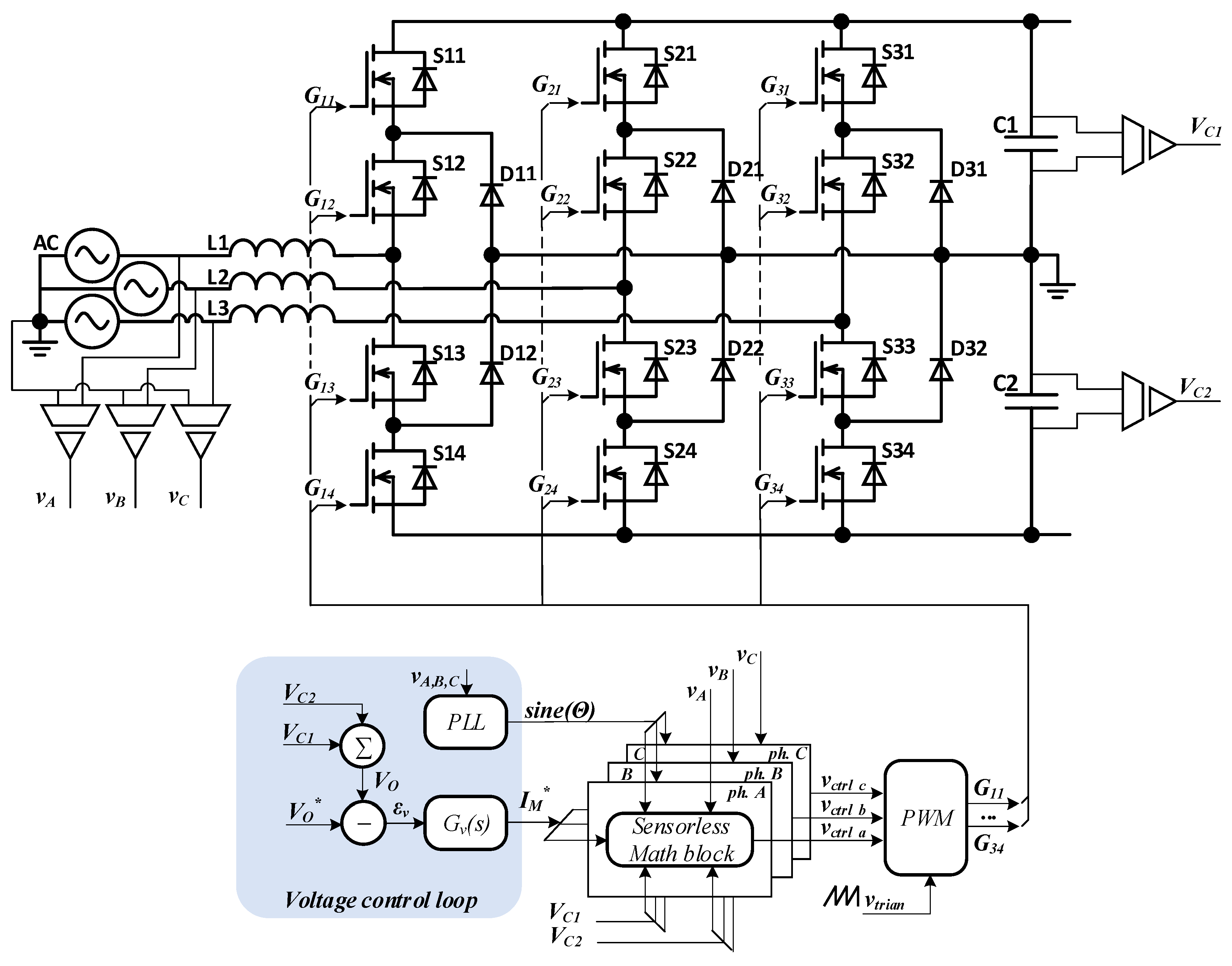
This paper studies the single-loop current sensorless control (SL, CSC, SL-CSC) approach applied to the three-phase four-wire three-level NPC MLC (see Figure 1) that could run without current sensors operating both in the rectifier and inverter modes. The paper is organised as follows: Section 2 describes the methods of the research, mainly focusing on the implementation of the SL CSC; Section 3 presents the results of the simulation analysis of the SC CCSC applied to the three-phase MLC. The conclusions are drawn at the end of the paper.

2. Methods

The single-loop controller uses only a single control loop with voltage feedback to stabilise the DC-bus voltage, while the current controller is replaced with the math block responsible for the duty cycle calculation based on the reference current value and acquired grid and DC-bus voltage values.

2.1. Switching State Table

The selected topology contains three L-type input filters, three legs of 3-level NPC block available in an “off-the-shelf” solution with standard module-type industrial packaging, as well as two DC link capacitors connected in series, while the middle point is connected to the diode’s middle point of all three NPC modules and also to the common neutral potential. Considering that the NPC MLC topology has four-wire connection, the analysis of the three-phase converter could be reduced to three identical and independent single-phase NPC MLCs with the capacitor middle point connected to the neutral wire. The current paths for different switching states are shown in Figure 2.
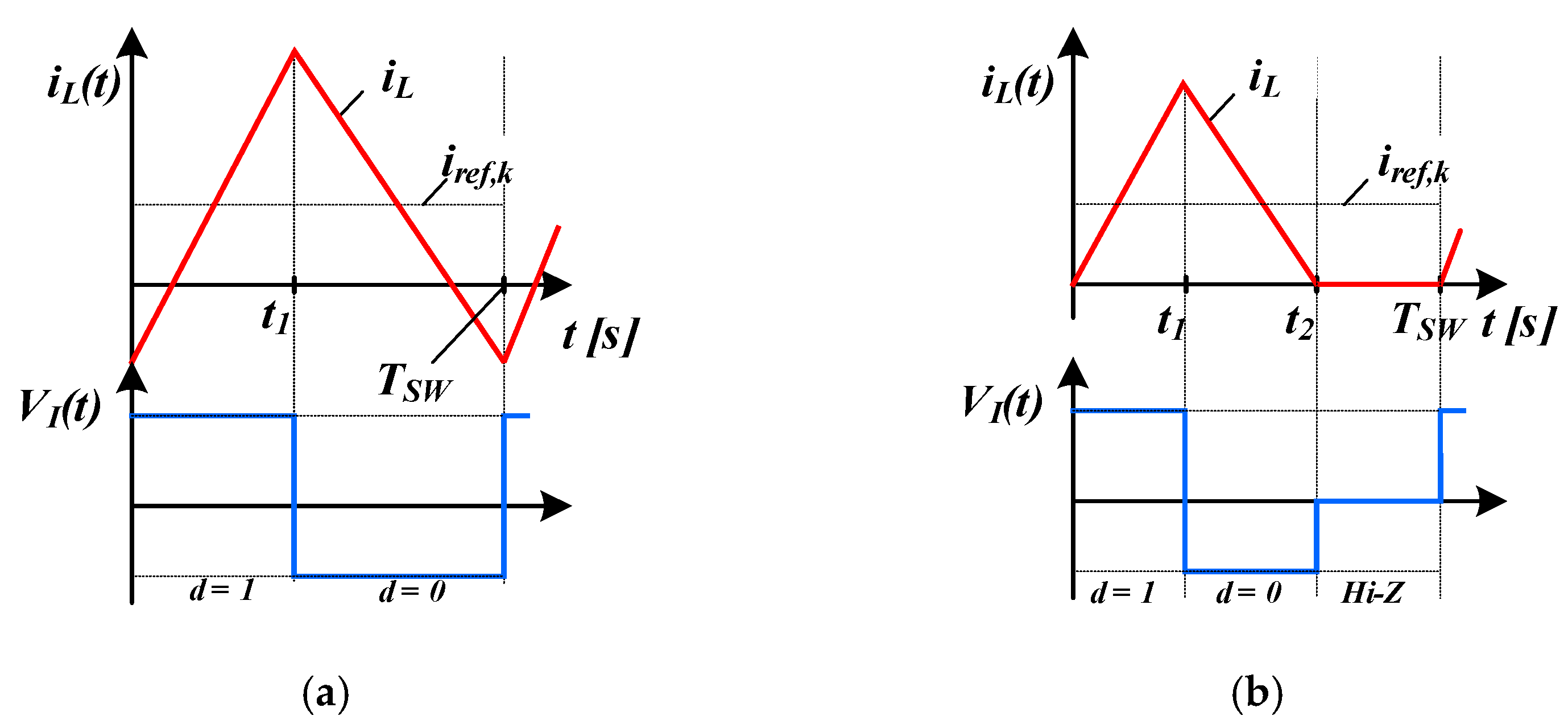
Different operation scenarios are possible during inductor’s current zero crossing: (1) bipolar voltage switching during the whole switching period that allows maintaining of the continuous current mode (CCM) and (2) bipolar voltage switching with a high-Z state period after the current drops to zero value. The latter considers the discontinuous current mode (DCM) in the inductor and thus is preferable. The reason is that the proposed CSC method inherits an accumulated volt-second error effect, resulting in current shape degradation during the CCM period [32]. Instead, the DCM operation allows resetting of the volt-second error during the current zero crossing, ensuring the current starts from the zero point in the following switching cycle, which helps to maintain a sinusoidal shape of the grid current (see Figure 3). It is obvious that the shorter the CCM period, the smaller is the accumulated volt-second error; as a result, the impact on the sinusoidal shape of the inductor’s current is negligible.
In case a converter operates in a wide range of power, including less than 10% of the nominal power, a higher efficiency is expected to be obtained by using DCM during zero crossing. The reason is that, depending on the input inductor size, the DCM period of the grid-side inductor could share a noticeable part of the grid period.
The switching table below (see Table 1) contains the corresponding inductor voltages and their impact on the capacitor voltages, where IM is the amplitude value of the reference current value (IM > 0—rectifier mode, IM < 0—inverter mode), d(t) is the control signal applied to transistors (1—inductor magnetisation state, 0—inductor demagnetisation state).

2.2. Current Sensorless Control

As mentioned previously, the main idea of the current sensorless control is to maintain a proper volt-second balance applied to a grid-side inductor to ensure that the average value of the inductor current can follow the reference value. In other words, the controller modulates the inverter’s output voltage by proper calculation of the magnetisation and demagnetisation periods to ensure the average inductor current follows a sinusoidal shape of the reference signal without the current feedback. For that purpose, the CSC block should be aware of the voltage levels to be applied to the inductor for the upcoming switching period.
In order to minimise the number of inductor voltage equations from Table 1, the single switch model can be applied to each phase of the converter that uses Boolean functions to track the voltage-source component changes in the current path as well as the polarity of the capacitors. In this relation, gtz(x) (greater than zero) is defined as follows:
g t z x = 1 ,   i f   x     0 0 ,   i f   x < 0 ,
This function allows reduction of the number of equations of the converter output voltage down to two for the magnetisation ( V I d = 1 t ) and demagnetisation states ( V I d = 0 t ):
V I d = 1 t = g t z I M · g t z v g t · v C 1 t g t z v g t · v C 2 t ,
V I d = 0 t = g t z I M · g t z v g t · v C 1 t g t z v g t · v C 2 t  
where v g t is the grid voltage, v C 1 t and v C 2 t are DC-bus capacitor voltages.
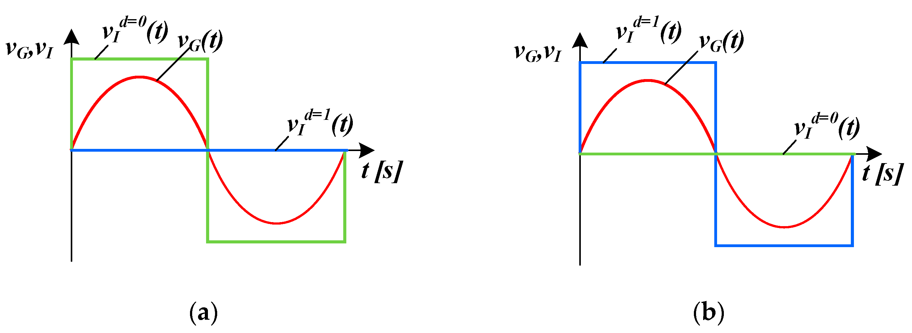
Depending on the grid voltage polarity and the direction of converter power flow (rectifier or inverter), the final values from the above-defined equations are visualised in Figure 4.
It is assumed that grid and capacitor voltages remain constant during a single switching cycle; thus, the inductor’s current rises and falls linearly, as shown in Figure 5.
Moreover, the time-variant inducto current can be transformed to discrete values by mathematical averaging in order to simplify the calculations within a single switching cycle:
I r e f , k = I a v g , k = 1 / T s w   k · T s w k + 1 · T s w I M   ·   sin t d t = 1 / T s w   k · T s w k + 1 · T s w i L t d t
where I r e f , k is the average reference value for the k-th switching period, I a v g , k is the average inductor current for the k-th switching period, T s w is the switching period,   I M is the amplitude of the reference signal.
The same average inductor current can be defined from the basic inductor equation, where the current depends on the applied voltage:
I a v g , k = 1 / T s w   k · T s w k · T s w + t 1 , k v G t v I d = 1 t L d t + k · T s w + t 1 , k k · T s w + t 2 , k v G t v I d = 0 t L d t
where v G t is the grid voltage, v I d = 1 t is the converter’s voltage during the magnetisation period, v I d = 0 t is the converter voltage during the demagnetisation period, L is the inductor’s inductance, the time slot from k · T s w to k · T s w + t 1 , k is the magnetisation period, the time slot from k · T s w + t 1 , k to k · T s w + t 2 , k is the demagnetisation period.
As we assumed previously that the grid voltage and capacitor voltages stay almost constant within a single switching cycle, it is reasonable to replace the time-variant voltage variables with discrete constant values, with the index k representing the number of the switching period.
Thus, Equation (5) can be rewritten as follows:
I a v g , k = 1 / T s w   V G , k V I , k d = 1 L   ·   t 1 , k + V G , k V I , k d = 0 L · t 2 , k t 1 , k .
The following equation defines the maximum inductor current during the magnetisation period:
I L m a x , k d c m = V G , k V I , k d = 1 L   ·   t 1 , k
where i L m a x , k d c m is the inductor’s maximum current during the k-th switching period.
The average current value during DCM can be also defined using the peak current value as follows:
I a v g , k = I L m a x , k d c m   ·   t 2 , k 2   ·   T s w
In addition, it is possible to define the ratio between the total current flowing period (t2) and the magnetisation period (t1):
t 2 , k = 1 V G , k V I , k d = 1 V G , k V I , k d = 0   ·   t 1 , k
Finally, it is possible to define the equation for the inductor’s magnetisation period to get an average current to follow the reference value during DCM by substituting the variable from Equation (8) for definitions from Equations (7) and (9):
D d c m , k = t 1 , k T S W = 2 · I a v g , k · L / T s w V G , k + V I , k d = 0 V G , k V I , k d = 1   ·   V I , k d = 1 V I , k d = 0
The magnetisation period during CCM can be calculated from Equation (6), where t2 is replaced with Tsw. The integration of the inductor’s voltage within a single switching period during CCM allows estimation of the end value of the current with respect to the starting point. Taking into account that the peak-to-peak value of the current remains almost constant between neighbouring switching cycles, the difference between the end value and the starting value is almost equal to the difference in the reference current between the neighbouring switching cycles (∆Iavg,k). Then the transistor’s control signal can be defined as follows:
D c c m , k = t 1 , k T S W = · I a v g , k · L / T s w V G , k + V I , k d t = 0 V I , k d t = 0 V I , k d t = 1
The minimal value of the two control equations should be finally applied to the transistors to implement CSC.

2.3. Controller Design

A PI controller is used to stabilise the DC-bus voltage that has positive and negative output value ranges, where positive values correspond to the rectifier mode, while the negative range activates the inverter mode (see Figure 6).
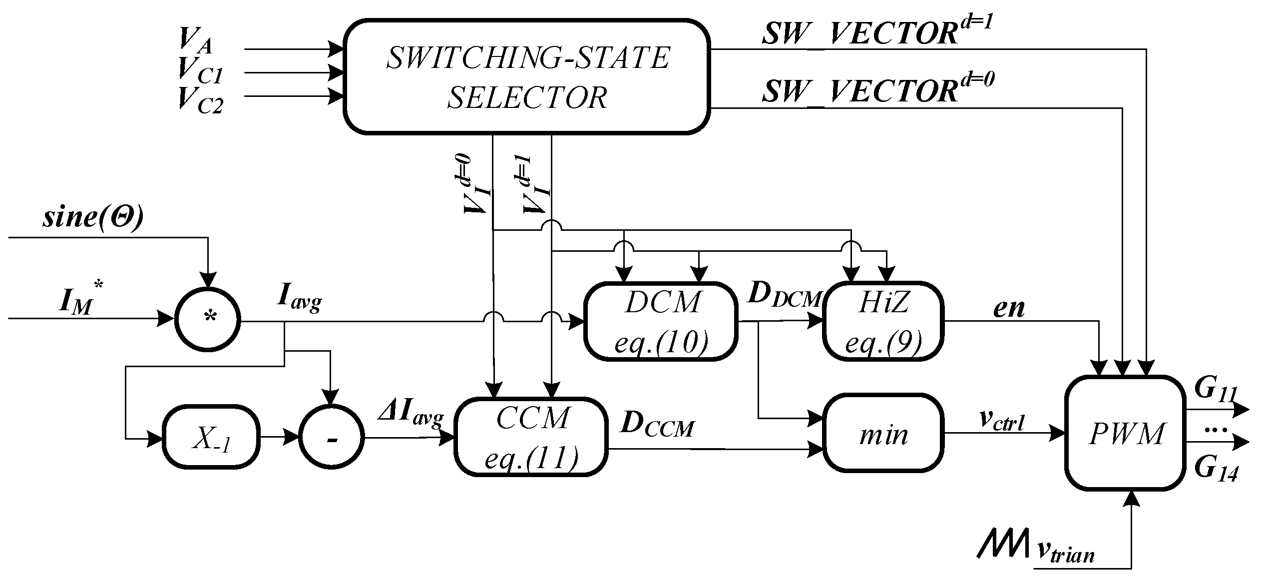
As can be seen from the figure above, each phase is provided with individual current control. Figure 7 shows a detailed block diagram of the sensorless math block.
It is worth mentioning that the table data (in the block diagram above) contain the switching states, and also the corresponding inductor voltage equation (in the form of a mask of used measurements presented in the inductor’s voltage equation), as well as the capacitor voltage differential. The CSC algorithm is not influenced by the table data, which means that by changing only the table data it is possible to apply the proposed algorithm to another multilevel topology. An example is the 9-level ANPC MLC topology [33].

2.4. Capacitor Voltage Balancing

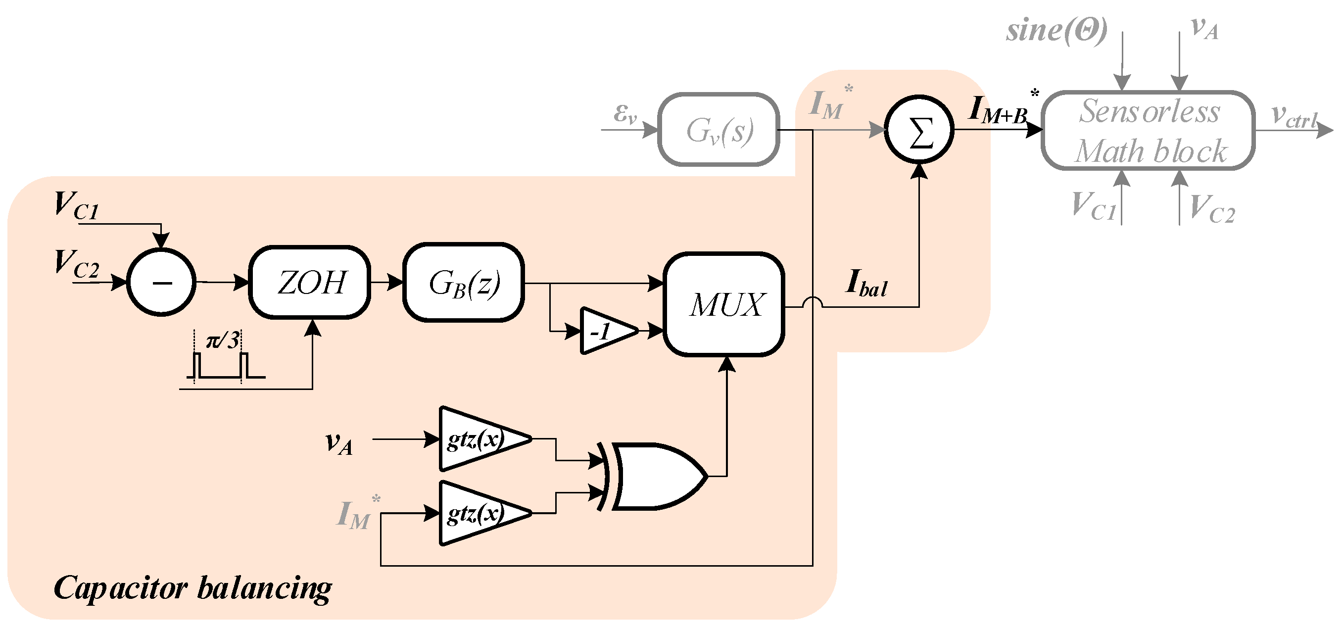
In ideal conditions, capacitor voltages fluctuating with triple grid frequency have voltage level crossing each π/3 angle starting from π/6. Nevertheless, due to the foreseen small imprecisions of CSC and manufacturer tolerances of the DC-link capacitors, capacitor voltage imbalance occurs in real world applications. Thus, an additional P-controller is implemented to adjust the reference current amplitude of phase A (see Figure 8).
The voltage difference of the two capacitors is applied to the PI-controller (kp = 0.1, kI = 0.1), whereas the output value is interpreted as an extra amplitude to the reference current of phase A. Since capacitor charging or discharging depends on the polarity of the input voltage and the power flow direction, an additional multiplexer that selects the sign of the balancing current amplitude is introduced. Finally, the summation of the balancing amplitude and the reference signal takes place and the result is supplied to the CSC math block.

3. Results

The proposed control method was evaluated by simulation analysis using the PSIM software. In the control algorithm, a simplified C-code block available from built-in PSIM control blocks was used.
The simulation parameters are as follows: grid voltage (RMS) VG = 230 V; grid frequency fAC = 50 Hz; capacitor nominal voltages VC1, VC2 = 400 V; inductance La,b,c = 1 mH; capacitance C1, C2 = 4.7 mF; switching frequency fsw = 20 kHz.

3.1. Rectifier Mode

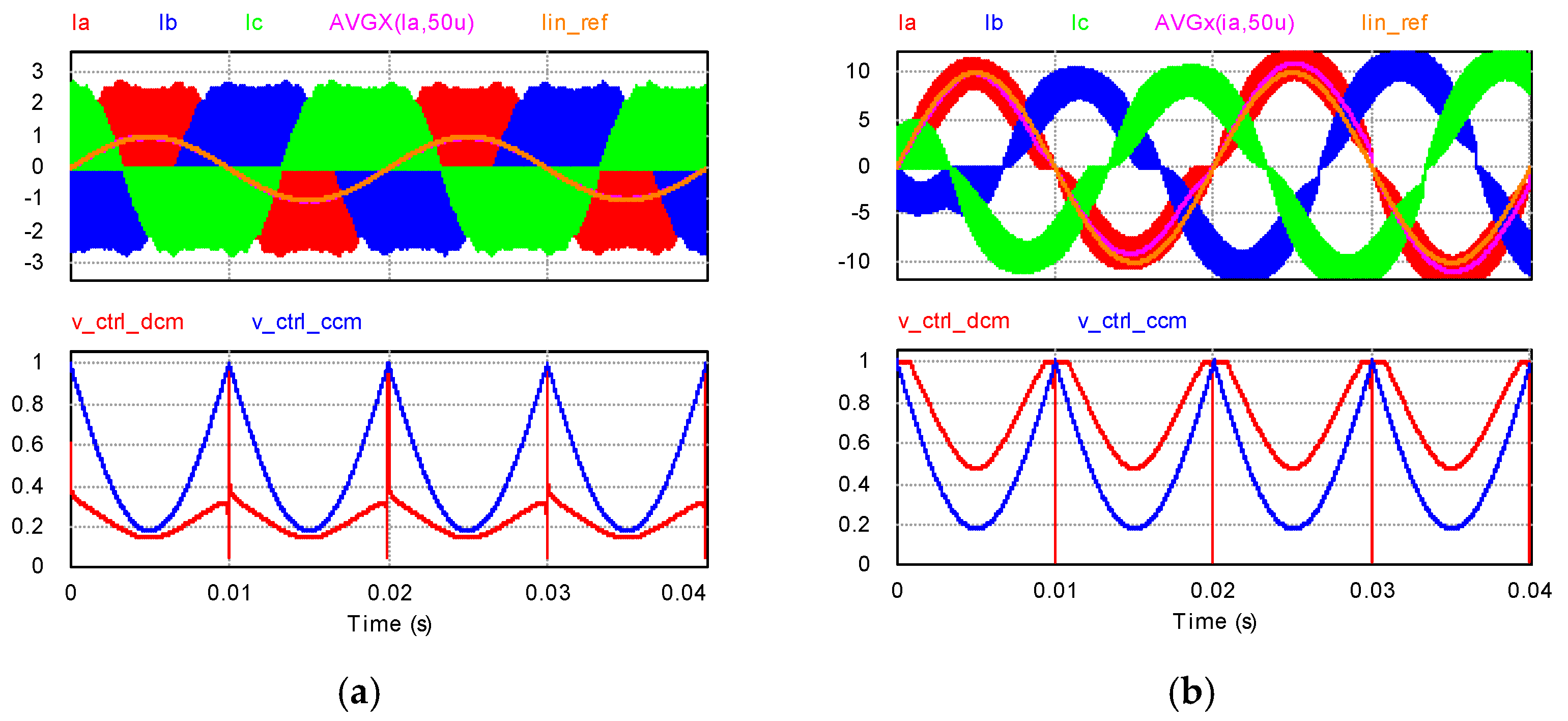
The rectifier mode was evaluated at two reference values: 1 A and 10 A. The first case (see Figure 9a) has DCM during the full input voltage period, shown by the bottom graph, where the DCM control signal has a lower value than the CCM control signal within the full grid period. Nevertheless, the average inductor current seen on the top graph perfectly matches the reference sinusoidal signal.
The second case (see Figure 9b) corresponds to 90% of the nominal power, where DCM takes place for a very short period near the zero crossing of the reference signal. The inductor operates mostly in CCM, which can be noticed by comparing the two control signals in the bottom graph of Figure 9b. An average current value follows the reference signal with minor deviation.

3.2. Inverter Mode

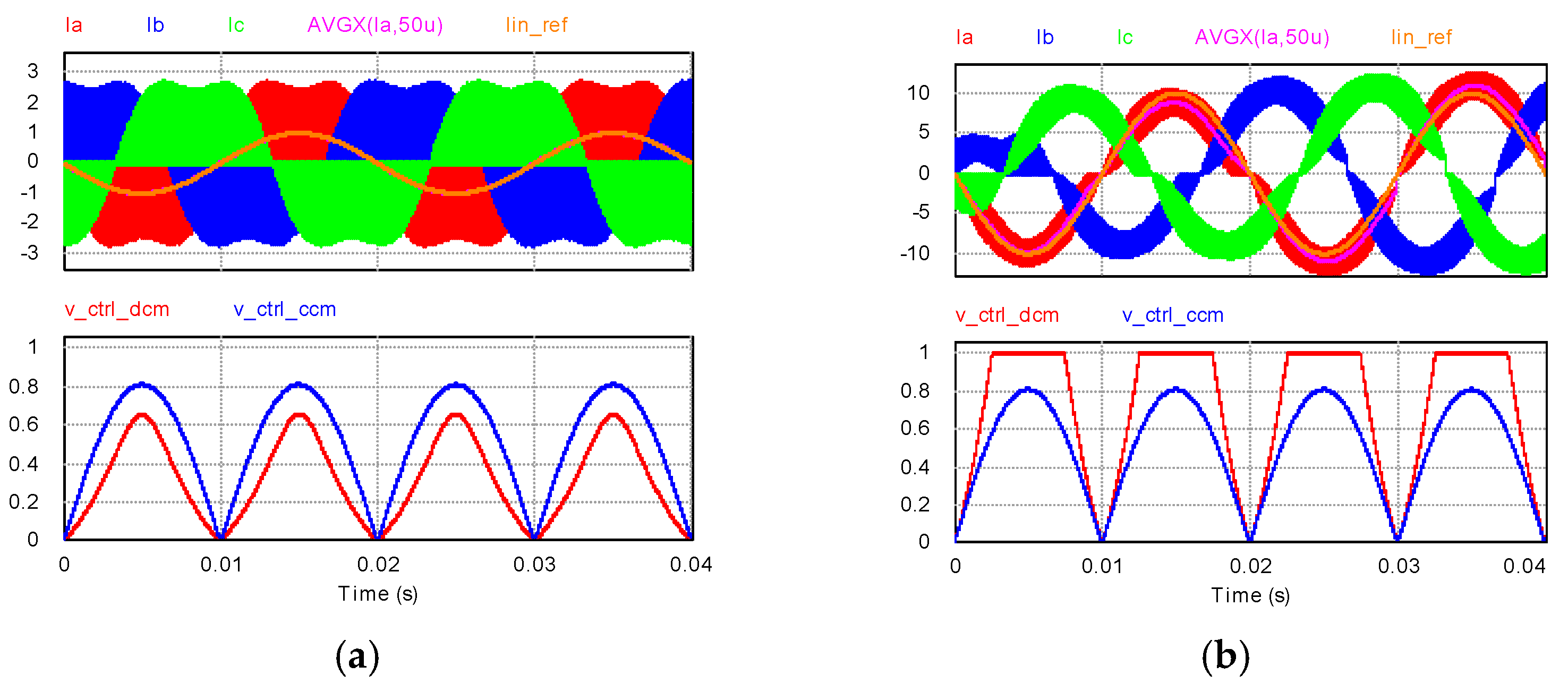
The inverter mode was simulated at two power points: −1 A and −10 A (see Figure 10). In both cases, the average current follows the reference value without any noticeable difference.
The current harmonic analysis is presented in the Table 2 for the inverter and rectifier modes at full power. The simulation results show that the harmonic distortion of the proposed controller meets the requirement of the IEC-61000-3-2 standard for a Class A device.

3.3. Capacitor Balancing

The capacitor balancing controller was tested by adding a 2.5 k resistor in parallel with capacitor C2 at time 0.1 s and activated at time 0.2 s. As can be seen from the figure, the two capacitor voltages are equalised 0.15 s after the balancing controller is activated (see Figure 11).

3.4. Step Response with Conversion Mode Change

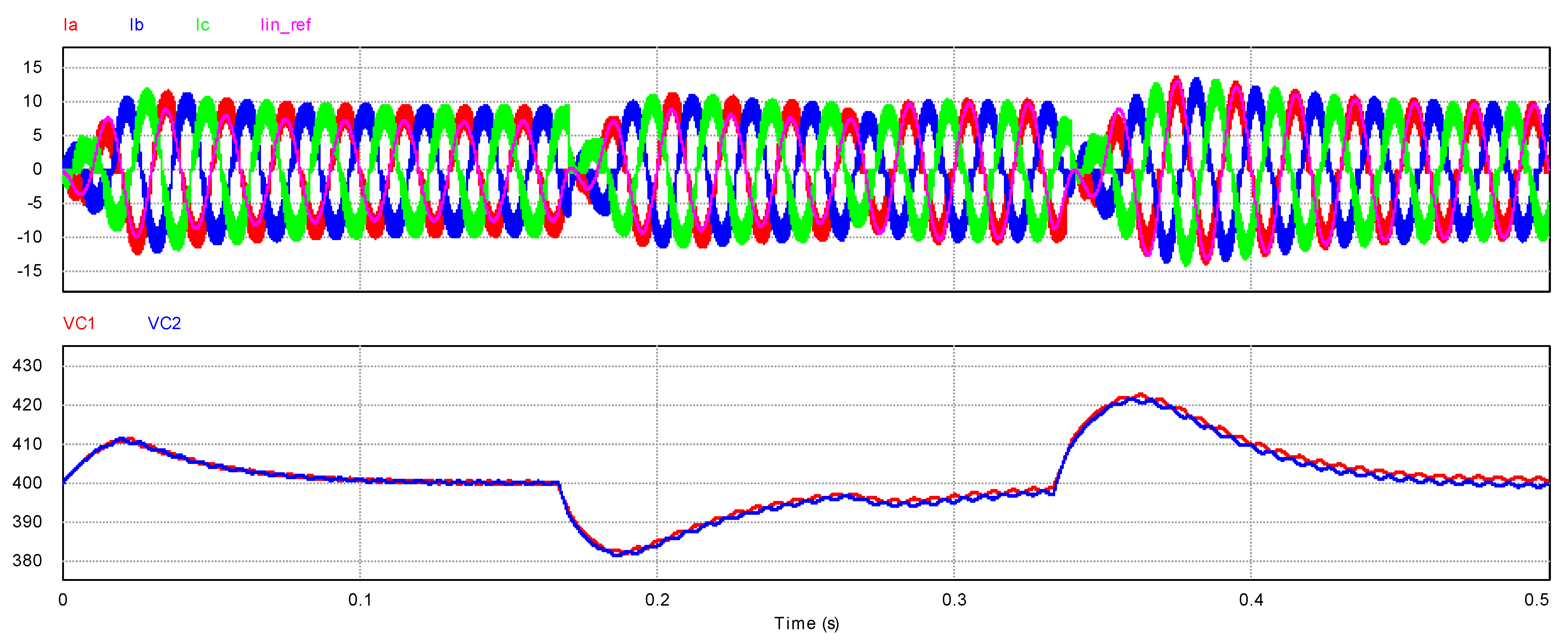
The step response simulation with the power flow direction change was performed by adding a 5 A controlled DC current source to the DC-bus driven by control pulses at 3 Hz, which resulted in 4 kW power sourcing or sinking from the DC-bus. The results of the simulation (see Figure 12) demonstrated good performance of the proposed SL-CSC that can stabilise the DC-bus voltage within 0.1 s. This performance is comparable to similar control system settling times found in the literature. For instance, a 100–150 ms settling time has been demonstrated in [28,31] at a load step change from 50% to 100%.

3.5. Grid Voltage Step Response

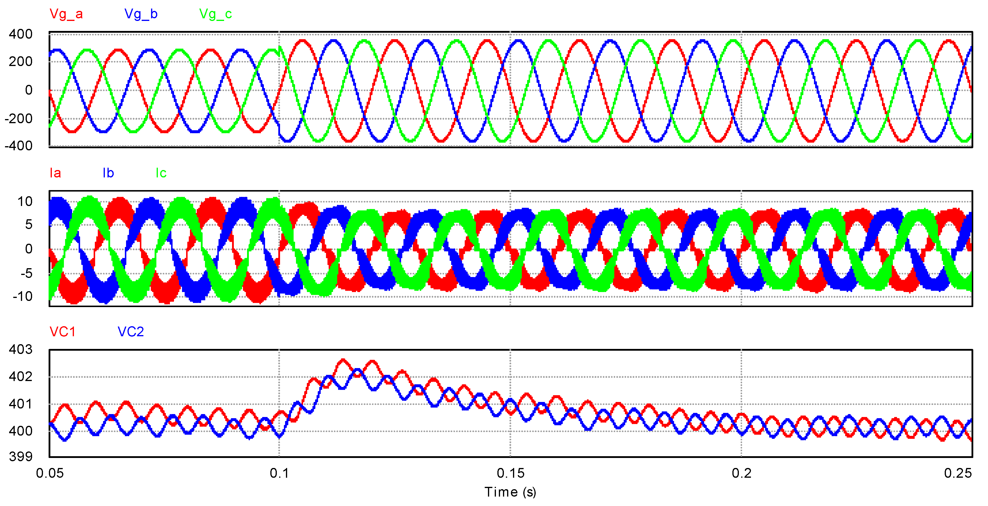
The grid voltage step response was simulated as well (see Figure 13). The proposed converter was operating at nominal power (4 kW) when the input voltage amplitude was changed from 292 to 357 V at time 0.1 s, which corresponds to the voltage step from 90% to 110% of the nominal amplitude (325 V). Some slight increase of the DC-bus voltage could be observed right after the step event. The reaction of the PI regulator resulted in the reduction of the grid current amplitude. The new equilibrium point was reached in 0.1 s after the voltage step event. Meanwhile, the CSC mathematical block reacted at the next switching period by recalculating the duty cycle signal that corresponds to the new grid voltage. Thus, the current shape of the inductor was not influenced.

4. Discussion and Conclusions

The single-loop current sensorless control (SL-CSC) algorithm was applied to a three-phase four-wire three-level neutral-point clamped multilevel converter (NPC MLC). This is the first application of the proposed sensorless approach to the mentioned topology. The paper gives a detailed analytical description of main operation modes with key equations describing the mathematical basis of the proposed control algorithm. It is based on a few simple equations intended for the estimation of the inductor’s voltage during the magnetisation and demagnetisation periods, which are used to calculate the corresponding duty ratio for the transistors. As a result, the average inductor current follows the reference value without the feedback from the current sensor, which allows for abolishing of the instantaneous current measurement in the control system and also the internal current control loop. Thus, only a single control loop with voltage feedback is finally used to stabilise the DC-bus voltage. This approach allows exclusion of the power losses related to shunt-based current sensors and an increase of the power density of the power electronics converter in the case where galvanically isolated current sensors are excluded.
The proposed algorithm suffers from an accumulated error effect during CCM of the inductor, which appears as a slowly increasing deviation from the reference value. This disturbance relates to the simplified mathematical equations used to estimate the inductor’s voltage where the conduction losses caused by parasitic circuit elements are neglected. Consequently, a small volt-second error takes place in each switching period, resulting in an increasing deviation of the inductor’s current from the reference value. Nevertheless, the paper describes the option of how to mitigate the described problem. The authors propose to use bipolar switching with high impedance state near the zero crossing that would ensure the DCM for the inductor. This helps to reset the accumulated error arising from the inductor’s current that starts from zero each new switching period during DCM. However, if the inductor operates in DCM during the whole grid voltage period, there is no noticeable deviation from the reference value.
The capacitor voltage balancing was implemented by means of an additional PI controller. It monitors the voltage difference six times per grid period, when the capacitors’ voltages should have identical values in the balanced condition. In the case of voltage error, it passes through the PI controller and the resulting extra current amplitude is added to the main reference value. The sign of the balancing current amplitude is modified according to the power direction flow and grid voltage polarity. Finally, the simulation analysis, where a 2.5 kOhm resistor was connected in parallel to capacitor C2, demonstrated an ability to compensate for the voltage asymmetry equal to 5 V in 0.15 s.
The simulation analysis demonstrated good performance of the proposed algorithm within a wide power range. The dynamic performance of the SL-CSC showed good results during the step response simulation with power direction change switching between a 4 kW source and 4 kW load connected to the DC-bus. The capacitor voltage overshoot stayed within 5% of the reference value with a settling time of 0.1 s, which is comparable to other similar control approaches mentioned in the literature. Moreover, the harmonic distortion of the proposed controller meets the requirements of the IEC 61000-3-2 standard for Class A devices.
Finally, it should be mentioned that the proposed current control algorithm could be easily modified for application to higher-level NPC MLC or even any other MLC topology. The mathematical block implementing the sensorless current control function is based on an invariant code written in the C programming language, while a specific description of the switching vectors is defined in the header file.
Further research is planned to include the experimental analysis and implementation of a hybrid (sensored and sensorless) control algorithm, demonstrating the benefits from both approaches.

Author Contributions

Conceptualisation, A.S.; methodology, A.S. and V.B.; simulation model, V.B.; formal analysis, J.Z. (Janis Zakis); writing—original draft preparation, A.S.; writing—review and editing, J.Z. (Jaroslavs Zarembo); visualisation, V.B.; supervision, A.S.; project administration, J.Z. (Jaroslavs Zarembo); funding acquisition, J.Z. (Jaroslavs Zarembo). All authors have read and agreed to the published version of the manuscript.

Funding

The paper is based on the research conducted in the framework of project No.1.1.1/20/A/068 funded by the ERDF. And this work has been supported by the European Regional Development Fund within the Activity 1.1.1.2 “Post-doctoral Research Aid” of the Specific Aid Objective 1.1.1 “To increase the research and innovative capacity of scientific institutions of Latvia and the ability to attract external financing, investing in human resources and infrastructure” of the Operational Programme “Growth and Employment” (No.1.1.1.2/VIAA/2/18/328).

Data Availability Statement

Data availability can be provided by contacting with corresponding author.

Conflicts of Interest

The authors declare no conflict of interest.

Abbreviations

ANPCasymmetric neutral point clamped
GaNgallium nitride
Hi-Zhigh ohmic input state
IGBTInsulated Gate Bipolar Transistor
MOSFETmetal oxide semiconductor field effect transistor
MLCmultilevel converter
NPC neutral point clamped
PELSpower electronics
PIDproportional integral regulator
PWMpulse width modulation
SiCsilicon carbide

References

  1. Chen, C. A Review of SiC Power Module Packaging: Layout, Material System and Integration. CPSS Trans. Power Electron. Appl. 2017, 2, 170–186. [Google Scholar] [CrossRef]
  2. Emon, A.I.; Mustafeez-ul-Hassan; Mirza, A.B.; Kaplun, J.; Vala, S.S.; Luo, F. A Review of High Speed GaN Power Modules: State of the Art, Challenges, and Solutions. IEEE J. Emerg. Sel. Top. Power Electron. 2022, 1. [Google Scholar] [CrossRef]
  3. Sidorov, V.; Chub, A.; Vinnikov, D.; Peng, F.Z. Survey of Topology Morphing Control Techniques for Performance Enhancement of Galvanically Isolated DC-DC Converters. IEEE Open J. Ind. Electron. Soc. 2022, 3, 751–777. [Google Scholar] [CrossRef]
  4. Yang, S.; Xiang, D.; Bryant, A.; Mawby, P.; Ran, L.; Tavner, P. Condition Monitoring for Device Reliability in Power Electronic Converters: A Review. IEEE Trans. Power Electron. 2010, 25, 2734–2752. [Google Scholar] [CrossRef]
  5. Gonzalez-Hernando, F.; San-Sebastian, J.; Garcia-Bediaga, A.; Arias, M.; Iannuzzo, F.; Blaabjerg, F. Online Condition Monitoring of Bond Wire Degradation in Inverter Operation. In Proceedings of the 2018 IEEE Energy Conversion Congress and Exposition (ECCE), Portland, OR, USA, 23–27 September 2018; IEEE: Piscataway, NJ, USA, 2018; pp. 4115–4121. [Google Scholar]
  6. Sun, P.; Gong, C.; Du, X.; Peng, Y.; Wang, B.; Zhou, L. Condition Monitoring IGBT Module Bond Wires Fatigue Using Short-Circuit Current Identification. IEEE Trans. Power Electron. 2017, 32, 3777–3786. [Google Scholar] [CrossRef]
  7. Kjaer, M.V.; Wang, H.; Blaabjerg, F. End-of-Life Detection of Power Electronic Converters by Exploiting an Application-Level Health Precursor. IEEE Open J. Power Electron. 2022, 3, 549–559. [Google Scholar] [CrossRef]
  8. Ronanki, D.; Williamson, S.S. Health Monitoring Scheme for Submodule Capacitors in Modular Multilevel Converter Utilizing Capacitor Voltage Fluctuations. In Proceedings of the IECON 2018—44th Annual Conference of the IEEE Industrial Electronics Society, Washington, DC, USA, 21–23 October 2018; IEEE: Piscataway, NJ, USA, 2018; pp. 2068–2073. [Google Scholar]
  9. Xiang, D.; Zheng, Y.; Li, H.; Gu, Y.; Zhao, N.; Zheng, J. Online ESR Monitoring of DC-Link Capacitor in Voltage-Source-Converter Using Damping Characteristic of Switching Ringings. IEEE Trans. Power Electron. 2021, 36, 7429–7441. [Google Scholar] [CrossRef]
  10. Suzdalenko, A.; Sribniya, V.; Zakis, J.; Huynh, K. Continuous Monitoring of Parasitic Elements in Boost Converter Circuit. In Proceedings of the 2021 IEEE 12th Energy Conversion Congress & Exposition—Asia (ECCE-Asia), Singapore, 24–27 May 2021; IEEE: Piscataway, NJ, USA, 2021; pp. 1829–1832. [Google Scholar]
  11. Chen, G.; Cheng, Q.; Wang, H.; Li, M.; Xu, C.; Deng, L. Study on bi-directional energy transfer of EV charging station on micro-grid operation. In Proceedings of the 11th World Congress on Intelligent Control and Automation, Shenyang, China, 29 June 2014–4 July 2014; IEEE: Piscataway, NJ, USA, 2014; Volume 2015, pp. 5517–5522. [Google Scholar]
  12. Guo, W.; Han, X.; Ren, C.; Wang, P. The control method of bidirectional AC/DC converter with unbalanced voltage in hybrid micro-grid. In Proceedings of the 2015 IEEE 10th Conference on Industrial Electronics and Applications (ICIEA), Auckland, New Zealand, 15–17 June 2015; IEEE: Piscataway, NJ, USA, 2015; pp. 381–386. [Google Scholar]
  13. Lv, Y.; Peng, Z.; Wang, Y. Design of A Novel 2.5kW Energy Storage Bidirectional Power Conversion System. In Proceedings of the 2021 IEEE 12th Energy Conversion Congress & Exposition—Asia (ECCE-Asia), Singapore, 24–27 May 2021; IEEE: Piscataway, NJ, USA, 2021; pp. 2022–2027. [Google Scholar]
  14. Vasiladiotis, M.; Christe, A.; Geyer, T. Model Predictive Pulse Pattern Control for Modular Multilevel Converters. IEEE Trans. Ind. Electron. 2019, 66, 2423–2431. [Google Scholar] [CrossRef]
  15. Wang, J.; Huang, J.; Liu, Z.; Liu, X.; Wang, Z. A Deadbeat Model Predictive Current Control Algorithm for Modular Multilevel Converters with Enhanced Steady-State Performance. In Proceedings of the 2021 IEEE International Conference on Predictive Control of Electrical Drives and Power Electronics (PRECEDE), Jinan, China, 20–22 November 2021; IEEE: Piscataway, NJ, USA, 2021; pp. 86–91. [Google Scholar]
  16. Sivakumar, S.; Natarajan, K.; Gudelewicz, R. Control of power factor correcting boost converter without instantaneous measurement of input current. IEEE Trans. Power Electron. 1995, 10, 435–445. [Google Scholar] [CrossRef]
  17. Chen, H.-C. Duty Phase Control for Single-Phase Boost-Type SMR. IEEE Trans. Power Electron. 2008, 23, 1927–1934. [Google Scholar] [CrossRef]
  18. Lopez-Martin, V.M.; Azcondo, F.J.; de Castro, A. Current error compensation for current-sensorless power factor corrector stage in continuous conduction mode. In Proceedings of the 2012 IEEE 13th Workshop on Control and Modeling for Power Electronics (COMPEL), Kyoto, Japan, 10–13 June 2012; IEEE: Piscataway, NJ, USA, 2012; Volume 23612, pp. 1–8. [Google Scholar]
  19. Chen, H.-C.; Liao, J.-Y. Bidirectional Current Sensorless Control for the Full-Bridge AC/DC Converter with Considering Both Inductor Resistance and Conduction Voltages. IEEE Trans. Power Electron. 2014, 29, 2071–2082. [Google Scholar] [CrossRef]
  20. Suzdalenko, A.; Zakis, J. Single-Loop Current Sensorless Control for Half-Bridge Based AC/DC Converter. IETE Tech. Rev. 2016, 33, 662–673. [Google Scholar] [CrossRef]
  21. Lu, C.Y.; Hsu, Y.W.; Chen, H.C. Design of Current Sensorless Control for Totem-Pole Boost PFC Converter. In Proceedings of the 2019 10th International Conference on Power Electronics and ECCE Asia (ICPE 2019—ECCE Asia), Busan, South Korea, 27–30 May 2019; Volume 3, pp. 986–991. [Google Scholar]
  22. Lopez, F.; Azcondo, F.J.; Corradini, L.; Lamo, P.; Pigazo, A. Third harmonic compensation in bridgeless current sensorless PFC. In Proceedings of the 2018 IEEE Applied Power Electronics Conference and Exposition (APEC), San Antonio, TX, USA, 4–8 March 2018; IEEE: Piscataway, NJ, USA, 2018; Volume 2018, pp. 2084–2090. [Google Scholar]
  23. Qi, T.Q.T.; Xing, L.X.L.; Sun, J.S.J. Dual-Boost PFC Converter Control without Input Current Sensing. In Proceedings of the 2009 Twenty-Fourth Annual IEEE Applied Power Electronics Conference and Exposition, Washington, DC, USA, 15–19 February 2009; IEEE: Piscataway, NJ, USA, 2009; pp. 1855–1861. [Google Scholar]
  24. Suzdalenko, A.; Zakis, J.; Steiks, I.; Chaiko, Y. Verification of current sensorless control for single-phase NPC multilevel inverter. In Proceedings of the 2015 9th International Conference on Compatibility and Power Electronics (CPE), Lisbon, Portugal, 24–26 June 2015; IEEE: Piscataway, NJ, USA, 2015; pp. 462–466. [Google Scholar]
  25. Suzdalenko, A.; Zakis, J.; Suskis, P.; Ribickis, L. Bidirectional single-loop current sensorless control applied to NPC multi-level converter considering conduction losses. Int. J. Power Electron. Drive Syst. 2020, 11, 1945–1957. [Google Scholar] [CrossRef]
  26. Pan, C.-T.; Chen, T.-C. Modelling and analysis of a three phase PWM AC—DC convertor without current sensor. IEE Proc. B Electr. Power Appl. 1993, 140, 201. [Google Scholar] [CrossRef]
  27. Roman-Loera, A.; Flores, L.A.; Rizo-Diaz, F.D.J.; Arambula-Miranda, L.E. Current sensorless predictive algorithm control for three-phase power factor correction. In Proceedings of the 2008 34th Annual Conference of IEEE Industrial Electronics, Orlando, FL, USA, 10–13 November 2008; IEEE: Piscataway, NJ, USA, 2008; pp. 653–658. [Google Scholar]
  28. Chen, H.-C.; Lu, C.-Y.; Li, G.-T. Design and Implementation of Three-Phase Current Sensorless Control for PFC Bridge Converter with Considering Voltage Drops of Power Semiconductors. IEEE Trans. Ind. Electron. 2018, 65, 9234–9242. [Google Scholar] [CrossRef]
  29. Santoyo-Anaya, M.A.; Rodriguez-Rodriguez, J.R.; Moreno-Goytia, E.L.; Venegas-Rebollar, V.; Salgado-Herrera, N.M. Current-Sensorless VSC-PFC Rectifier Control with Enhance Response to Dynamic and Sag Conditions Using a Single PI Loop. IEEE Trans. Power Electron. 2018, 33, 6403–6415. [Google Scholar] [CrossRef]
  30. Suzdalenko, A.; Zakis, J.; Husev, O. Development of single-loop current sensorless control for bidirectional three-phase PWM rectifier. In Proceedings of the 2015 56th International Scientific Conference on Power and Electrical Engineering of Riga Technical University (RTUCON), Riga, Latvia, 14 October 2015; IEEE: Piscataway, NJ, USA, 2015; Volume 1, pp. 1–4. [Google Scholar]
  31. Li, C.-Y.; Chao, N.-C.; Chen, H.-C. Design and Implementation of Four-Switch Current Sensorless Control for Three-Phase PFC Converter. IEEE Trans. Ind. Electron. 2020, 67, 3307–3312. [Google Scholar] [CrossRef]
  32. Suzdalenko, A.; Zakis, J. Study of Disturbing Factors in Current Sensorless Control Applied to NPC MLC. In Proceedings of the 2020 IEEE 14th International Conference on Compatibility, Power Electronics and Power Engineering (CPE-POWERENG), Setubal, Portugal, 8–10 July 2020; IEEE: Piscataway, NJ, USA, 2020; pp. 156–160. [Google Scholar]
  33. Suzdalenko, A.; Van Khang, H.; Zakis, J.; Sribniya, V. Nine-Level Active Neutral Point Clamped Converter with Cascading H-bridges Fed by Flying Capacitors. In Proceedings of the ICPES 2021, Shanghai, China, 18–20 December 2021; IEEE: Piscataway, NJ, USA, 2021; pp. 1–5. [Google Scholar]
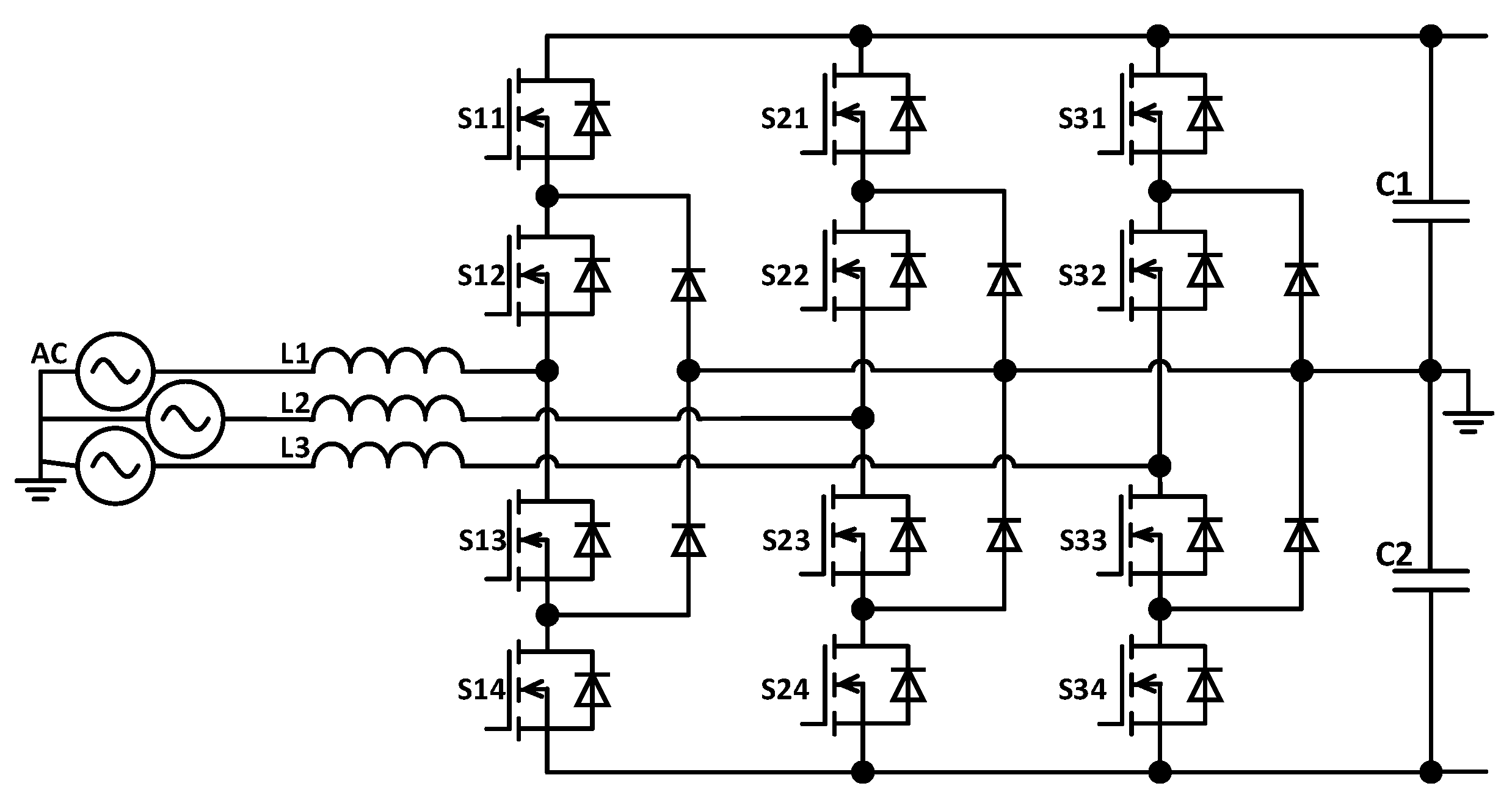
Figure 1. Three-phase four-wire three-level NPC inverter topology.
Energies 16 04599 g001
Figure 2. Commutated current paths according to the selected voltage pole: (a) level 1 (voltage pole +VDC/2), (b) level 0, and (c) level −1 (voltage pole −VDC/2).
Energies 16 04599 g002
Figure 3. Preview of current control approaches during zero crossing: (a) bipolar switching where the inductor current operates in CCM and (b) bipolar switching with Hi-Z state where the inductor current operates in DCM.
Energies 16 04599 g003
Figure 4. Analytical shapes of converter modulated voltages: (a) rectifier mode and (b) inverter mode.
Energies 16 04599 g004
Figure 5. Simplified current shapes and corresponding parameters during (a) DCM and (b) CCM.
Energies 16 04599 g005
Figure 6. Block diagram of the single-loop CSC algorithm.
Energies 16 04599 g006
Figure 7. Block diagram of the “sensorless math-block” for phase A.
Energies 16 04599 g007
Figure 8. Block diagram of the capacitor balancing controller added to phase A CSC.
Energies 16 04599 g008
Figure 9. Simulation results of the rectifier mode: (a) reference value IM = 1 A and (b) reference value IM = 10 A (x-axis is time [s], top graph y-axis is current [A], bottom y-axis is duty ratio [%]).
Energies 16 04599 g009
Figure 10. Simulation results of the inverter mode: (a) reference value IM = −1 A and (b) reference value IM = −10 A (x-axis is time [s], top graph y-axis is 3-phase current, average A-phase current and A-phase reference current [A], bottom y-axis is SL-CSC calculated duty ratio for DCM and CCM [%]).
Energies 16 04599 g010
Figure 11. Simulation result of the capacitor balancing controller (x-axis is time [s], top graph y-axis is phase A current [A], middle y-axis is capacitor voltages [V], bottom y-axis is balancing current [A]).
Energies 16 04599 g011
Figure 12. Simulation results of step response with the bidirectional power flow (x-axis is time [s], top graph y-axis is 3-phase current and A-phase reference current [A], bottom y-axis is capacitor voltages [V]).
Energies 16 04599 g012
Figure 13. Simulation results of grid voltage step response (x-axis is time [s], top graph y-axis phase voltages [V], middle graph y-axis phase voltages [A], bottom graph y-axis capacitor voltages [V]).
Energies 16 04599 g013
Table 1. Switching states of the bidirectional 3-phase 4-wire 3-level NPC MLC for phase A.
Power ModeGrid
Polarity
Voltage LevelVoltage PolePWM
Output
d(t)
Transistor Conduction StateSimplified Inductor VoltagedVc1dVc2
Sx1Sx2Sx3Sx4
Rectifier
(IM > 0)
Positive (Va > 0) 1--1-VL = Va00
00011--VL = VaVC1+∆0
Negative (Va > 0)1+Vdc/21-1--VL = Va00
000--11VL = Va + VC20+∆
High-Z (IM = 0)-−1Vdc/2-----VL = 0--
Inverter
(IM < 0)
Positive (Va > 0)Z-111--VL = VaVC1−∆0
1+Vdc/20-1--VL = Va00
Negative (Va > 0)001--11VL = Va + VC20−∆
−1+Vdc/20--1-VL = Va00
Table 2. Harmonic analysis of input current.
Order of Current HarmonicsClass A LimitPhase A Current
Rectifier (4 kW)Inverter (−4 kW)
Fundamental-10.110.1
Even32.30.110.07
51.140.110.1
70.770.0920.082
90.40.0750.069
110.330.0560.052
130.210.050.046
15 ≤ h ≤ 390.15<0.05<0.04
Odd21.080.1470.131
40.430.0140.02
60.30.0310.033
8 ≤ h ≤ 400.23<0.03<0.02
Disclaimer/Publisher’s Note: The statements, opinions and data contained in all publications are solely those of the individual author(s) and contributor(s) and not of MDPI and/or the editor(s). MDPI and/or the editor(s) disclaim responsibility for any injury to people or property resulting from any ideas, methods, instructions or products referred to in the content.