Article

Performance Assessment of a Grid-Connected Two-Stage Bidirectional Converter for a Combined PV–Battery Energy Storage System †

1
MOBI-EPOWERS Research Group, ETEC Department, Vrije Universiteit Brussel, Pleinlaan 2, 1050 Brussels, Belgium
2
Flanders Make, 3001 Heverlee, Belgium
*
Author to whom correspondence should be addressed.
This paper is an extended version of our papers published in the 2022 Second International Conference on Sustainable Mobility Applications, Renewables and Technology (SMART), 23–25 November 2022.
Energies 2023, 16(11), 4486; https://doi.org/10.3390/en16114486
Submission received: 25 March 2023 / Revised: 26 May 2023 / Accepted: 29 May 2023 / Published: 1 June 2023

Abstract

:
This paper presents a comprehensive performance assessment of a two-stage power electronic (PE) converter for interfacing the grid of a lithium-ion battery energy storage system (Li-BESS) for building-integrated PV (BIPV) applications. A performance assessment of the control system was conducted for the two-stage PE interface with a common DC-link, which consisted of a bi-directional boost converter with a cascaded PI controller and an AC/DC converter with proportional-integral (PI) and proportional-resonant (PR) controllers. The assessment covered loss analysis and useful lifetime estimation for the 10 kW PE interface with a wide-bandgap SiC power MOSFET at different loads for both the charging and discharging modes of a 50 kWh lithium-ion battery system. Additionally, a performance comparison of various switching frequencies was performed. It was observed that the system was stable up to a switching frequency of 30 kHz, and that increasing the switching frequency improved the responsiveness of the converter by decreasing the settling time; however, there were diminishing returns at higher switching frequencies. To obtain a proper balance between responsiveness and lower loss, a switching frequency of 10 kHz was selected.

1. Introduction

Ensuring energy resilience and reaching net zero emissions by 2050 while electricity demands are increasing calls for the faster adoption of renewable sources (e.g., solar PV, wind). The incremental energy demand of the building sector is projected to be 70% by 2050 due to the electrification of heating systems [1]. At the same time, building-integrated PV (BIPV) systems are being increasingly used and interfaced with the grid. The BIPV market has increased substantially, reaching 500 MWp in 2022, and is expected to reach 726 MWp by the end of 2023 [2]. Battery system and PE interfaces are two significant entities to exploit in such combined PV systems. In stationary battery energy storage systems, Li-ion batteries (LIBs) are being increasingly used in comparison with other battery technologies. The relevant studies reveal that 80% of the installed stationary energy storage systems were LIB-based in 2020, and a compound annual growth rate of 17.4% is expected during 2022–2030 [3,4]. This is mainly due to the higher cycle life, lower self-discharge rate, higher charging and discharging efficiencies, and lower cost trending due to the homogeneous nature of LIBs in stationary and electromobility applications resulting in huge market share [5,6].
However, the performance of PE interfaces, such as AC/DC and DC/DC converters, used in the PV combined with battery energy storage system (BESS) plays a vital role in ensuring an optimal conversion from supply to demand. For grid-interfacing AC/DC converters, the injected grid current distortion level is one of the key parameters linked to power quality. In that regard, IEEE Standard 1547-2003 and IEC Standard 61727 have urged ensuring less than 5% of the total harmonic distortion (THD) for the grid current [7,8]. Additionally, the converter for such energy storage systems can suffer from different stability issues due to the shared DC-link voltage and strict power quality requirements. The DC/DC converter is critical to charging and discharging the battery system with improved battery roundtrip energy efficiency and battery lifetime [9]. In addition, passive components and control techniques that are applied in the power converter system can support reaching the standard power delivery for the PV combined with BESS application.
Furthermore, it has been reported that the performance of the PE interface, as determined by the controller, can have a significant impact on the selected components and may result in failure due to the operational stress induced by load requests, applied voltage, current, and generated heat [10]. Consequently, the lifetime of the PE interface may be reduced, thereby necessitating additional maintenance requirements and causing downtime for system servicing.
Several works have been carried out exploring PE interface design and assessment for PV–BESS applications. In [11], the authors designed a grid-interfacing AC/DC converter for a PV–BESS application in which they showed that with the designed passive components and control (current and voltage), it could achieve the highest efficiencies of 95.98% and 95.55% in the charging and discharging modes, respectively, at full-load operation. Moreover, in [12], the authors studied the quality of the feed-in grid current from single-phase inverters by designing a tailor-made current controller composed of a proportional-resonant controller (PR) and an RC controller. The study showed that a THD of 2.28% for the grid current could be achieved. However, other control strategies of the current have been advocated to reduce THD, such as PI, PR, current hysteresis, dead beat, model-predictive, and cascaded harmonic control [13,14]. However, PR is the most popular strategy in terms of implementation because it avoids Park transformations and requires less computational power for current regulation in single-phase PV applications [15,16].
Moreover, in [17], the authors studied the full-bridge bidirectional DC/DC converter for battery charging and discharging, where the maximal efficiency of the DC/DC converter was measured to be 96.0% during battery charging and 96.9% during discharging. In addition, in [18], a robust controller was designed for the DC/DC converter with the isolation structure of a voltage-fed dual active bridge to prevent battery voltage overshoot while achieving an efficiency of 95% for both modes of operation.
The aforementioned references have thoroughly studied the grid and battery side conversions in terms of proposed controllers and passive components with a fixed switching frequency. The system performance under the influence of switching frequency has not been investigated for such an application. Moreover, the reliability has not been considered in the design and assessment of the converters, while it can have a critical impact on the system’s service lifetime [19].
The primary contribution of this research lies in the development of a control system capable of effectively managing partial loading within a stable region. Furthermore, the research focuses on analyzing the electro-thermal performance of the system while varying the switching frequency for the controllers. The investigation of lifetime modeling and the impact of varying the system and control parameters is also a significant aspect of this work. In summary, the novelty of this research centers around an assessment of performance and control parameter variation for a two-stage bidirectional converter under different load transients, while also examining control stability. Additionally, the study estimates the lifetime of the converter by considering various stress factors.
The organization of this paper is as follows: in Section 2, the modeling of the PE interface and battery is discussed. Section 3 covers the corresponding control of the PE interface. In Section 4, the lifetime estimation of the PE converter is detailed. Finally, the results and discussion are presented in the concluding section, which includes the performance of control, electrical parameters, losses, and useful lifetime prediction.

2. Battery Energy Storage System Modeling

The design of the two-stage bidirectional converter for interfacing the grid of a stationary energy storage system is illustrated in Figure 1. The battery pack was charged and discharged from the single-phase AC power grid. Full-bridge AC/DC (230 Vrms to 400 Vdc) and half-bridge DC/DC (400 Vdc–200 Vdc) power stages were used by coupling a common DC-link for bidirectional power flow. The DC-link in the topology of the highlighted section was used to inject the PV power by using a boost DC/DC converter to the DC-link voltage. Please note that, in this paper, positive power flow is defined as the charging state and negative power flow is defined as the discharging state of the battery pack. For grid synchronization, generally a phase locked loop (PLL) is used for grid-interfaced converter. The single-phase PLL can be implemented using the Hilbert transformation. In this work, the single-phase feedforward PLL was implemented. Additionally, as shown in Figure 1, the complementary switching signals for the MOSFET(Q) switches—Q1 and Q2—are denoted by S1 and S2, respectively, in the AC/DC converter. Notably, during charging operation, Q1 and Q4 were turned on, whereas during discharging operation, the Q2 and Q3 switches were turned on. It is important to mention that the switching signals were converted into the dq frame during AC/DC converter modeling. In addition, Q5 was turned on during battery charging, and vice versa during battery discharging. The duty cycle, represented by D, served as the control signal for the DC/DC converter.

2.1. Modeling of AC/DC Converter

The active front-end converter was utilized for grid interfacing with a high-order passive filter (LCL filter), as per the topology utilized. The LCL filter comprises two inductances, Ls and Lc, for the grid and converter sides, respectively, along with the resistances of the series inductance, rs and rc. The filter capacitance is represented by Cf, with damping resistance Rd. Among these parameters, Lc holds the most significance in the voltage source converter [20]. The DC side of the converter is characterized by the DC-side capacitor, Cdc, DC-side voltage, vdc, and DC-link current, idc. The switching operation in the synchronously rotating dq frame is represented by the functions Sd and Sq. The mathematical model of a single-phase voltage-source converter is formulated in the synchronous dq frame using single-phase feedforward modeling, as presented in Equations (1) to (3) [21,22], where v d and v q serve as the dq components of the AC input voltage; i d and i q are the corresponding currents; and ω is the angular frequency.
v d = ( L s + L c ) d i d d t + r s i d ω L s i q + S d v d c
v q = ( L s + L c ) d i q d t + r s i q + ω L s i d + S q v d c
C d c d v d c d t = 3 2 ( i d S d + i q S q ) i d c

2.2. Modeling of DC/DC Converter

A bidirectional DC/DC power converter is required to regulate battery voltage (low side), which changes with state of the charge (SoC) and reaches the DC-link voltage (high side) while transferring power in the charging (buck) and discharging (boost) modes. The power stage dynamics of the DC/DC converter are modeled using Equations (4) and (5), utilizing an inductor and capacitor denoted by L0 and C0, respectively, with damping resistor R0 as a filter while charging the battery. In addition, the duty ratio is denoted by d r , and λ serves as the derived coefficient during discharging mode. When formulating the transfer function (Gid) for the buck and boost modes, the load (battery) is considered with resistance RL. The current through the load and voltage across the load are denoted by iL and vL, respectively. The control transfer functions of the charging and discharging modes for the converter are given below in Equations (6) and (7), where s and Gid are the representations of the Laplace operator and open loop transfer function for both modes, respectively. Further details regarding the modeling of the bidirectional DC/DC converter can be found in references [23,24].
L 0 d i L d t = 2 V d c d r + ( 2 λ 1 )   v L + v d c
C 0 d v L d t = i L v L R L
G i d = i L d r = 2 V d c ( s C 0 + 1 R L ) L 0 C 0 s 2 + L 0 R L s + 1     ( Buck   mode )
G i d = i L d r = V d c ( s C 0 + 2 R L ) L 0 C 0 s 2 + L 1 R L s + 2 λ 2   ( Boost   mode )

2.3. Li-Ion Battery

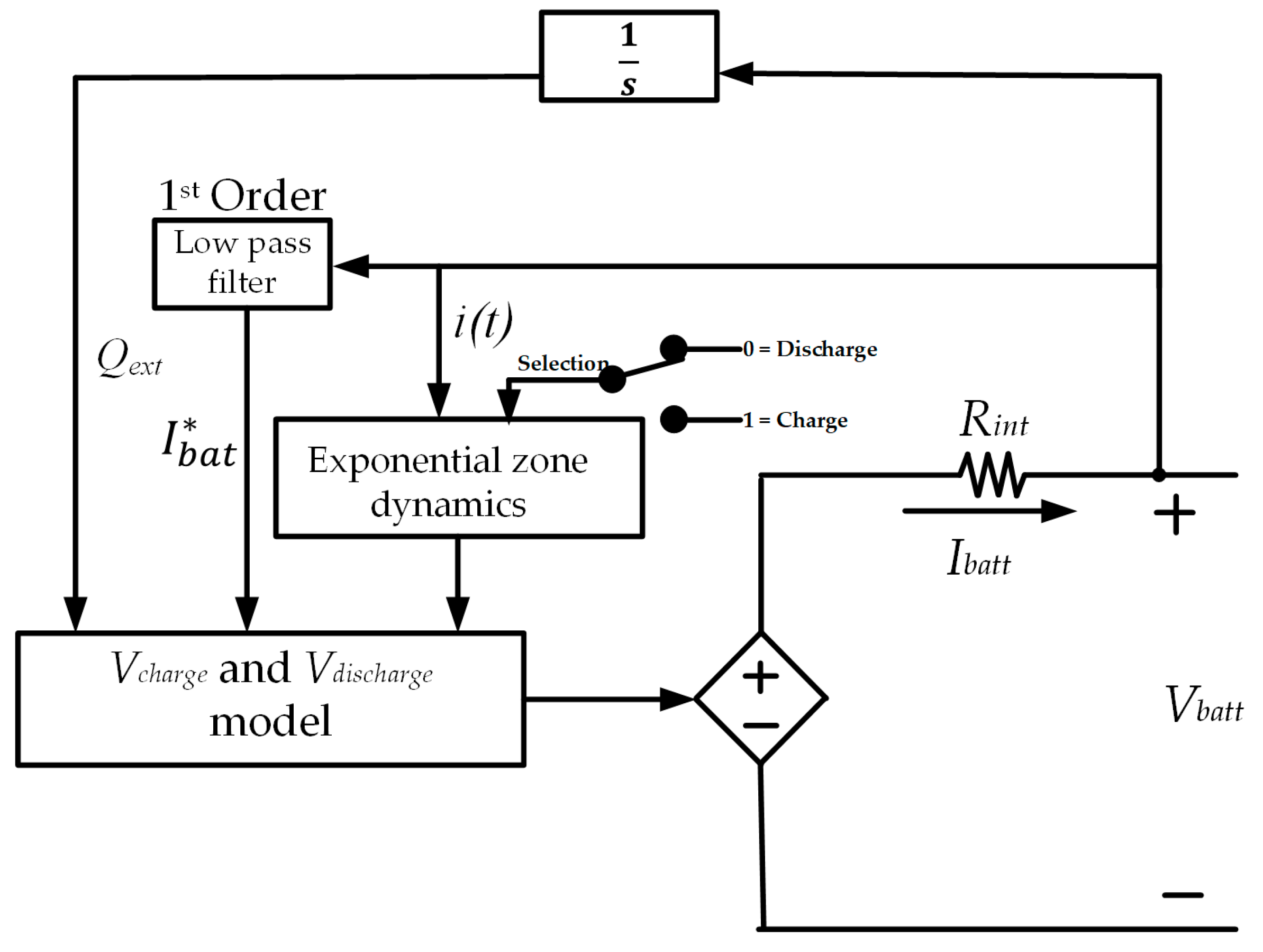
The modeling of a lithium-ion battery involves the use of an electrical equivalent circuit in order to effectively map the various dynamics of this chemistry [25]. A simple internal resistance-based model is widely used for battery voltage, current, and SoC performance [26,27]. The simple lithium-ion/LFP model [28] adopted here is illustrated in Figure 2. In the figure, the Vcharge and Vdischarge states are modeled by Equations (8)–(10):
V c h a r g e = V 0 K · Q m a x Q m a x Q e x t   · I b a t * K · Q m a x Q m a x Q e x t · Q e x t + A · e x p ( B · Q e x t )
V d i s c h a r g e = V 0 K · Q m a x Q e x t + 0.1 · Q m a x · I b a t * K · Q m a x Q m a x Q e x t · Q e x t + A · e x p ( B · Q e x t )
Q e x t = 0 t I b a t d t
where V0 represents the constant voltage (V); K denotes the polarization resistance (Ω); I b a t * denotes the filtered current (A); Q m a x and Q e x t refer to the maximum and extracted capacities (Ah), respectively; A represents the exponential voltage (V); and B represents the exponential capacity (Ah−1).

3. Control Design for the Two-Stage Bidirectional Converter

The stability of a PE converter’s operation is heavily dependent on the effectiveness of its control system. Generally, a two-stage power converter can maintain stability within a specific range of switching frequencies, each of which has a unique cut-off frequency closely related to the PE device’s switching frequency. This switching frequency, which determines the rate at which devices switch on and off to control the power flow, must be sufficiently below the cut-off frequency to avoid system instability and aliasing. Thus, the cut-off frequency is a critical parameter in the design of PE control systems as it affects the stability, response, and bandwidth of the system. Furthermore, variations in switching frequency can impact system efficiency, as electro-thermal performance differs depending on the frequency of operation. Therefore, careful consideration of the cut-off frequency is essential to ensure the system’s performance and reliability.
In line with the two-stage bidirectional converter concept in Section 2, the AC/DC interface used a PI controller for controlling the voltage and a PR controller for controlling the current to improve the system’s stability. For the battery side, a PI control was used to control the battery voltage and current. A brief description of the applied control strategy for the assessment is presented in the subsequent sections.

3.1. Control of AC/DC Converter

In this study, a feedforward control strategy was implemented, which consisted of the voltage controller as the external loop and current controller as the inner loop for the d-axis and q-axis current control [21]. The v d * and v q * references can be determined by following Equations (11) and (12), respectively. Consequently, the injected current can be modeled according to Equations (13) and (14). Finally, vd and vq can be represented as a function of v d * and v q * and i d and i q , as shown in Equations (15) and (16), where Kp and Ki are the gains of the PR controller.
v d * = L s d i d d t + r s i d
v q * = L s d i d d t + r s i d
i d ( s ) = 1 s L s + r s v d * ( s )
i q ( s ) = 1 s L s + r s v q * ( s )
v d = e d + ω L s i q ( K p + 2 K i s s 2 + ω 2 ) (   i d * i d )
v q = e q + ω L s i d ( K p + 2 K i s s 2 + ω 2 ) (   i q * i q )
The voltage and current controllers are designed based on the controller time constants, τv and τi, respectively. The current controller performs four to five times quicker than the voltage controller. However, the PR controller was adopted because of its advantageous resonant term to grid frequency and simplicity for development. For this reason, the PR controller was used in the current controller to improve controller performance. The gains of the PI and PR controllers are determined following Equations (17)–(22):
K p v = c o s θ | G p v ( s ) |
K i v = ω c s i n θ | G p v ( s ) |
θ = 180 φ m + G p v ( s )
K p i = G n ( ω n 2 ω 2 ) ω n
K i i = ω 2 K p i
ω n =   1 L s C d c
where K p v   and K i v represent the PI controller gain for the voltage control loop, while K p i and K i i are the gains for the current control loop. G n , ω n , and ω c respectively symbolize the controller’s proportionality gain, natural oscillation frequency, and cut-off frequency. Gpv(s) refers to the open-loop transfer function, while φm represents the phase margin in degrees, which is obtained from the Bode plot of the open-loop transfer function.

3.2. Control of DC/DC Converter

A cascaded control structure was used for the bidirectional DC/DC converter. The closed-loop current and voltage controller equations are presented in Equations (23) and (27). This also comprises the voltage controller as an outside level and the current controller as an inside level, where the inside level performs tenfold quicker than the outside level. The inside level regulates the average inductor current, iL0, using a PI controller. The continuous duty ratios from the controllers were then sent to the PWM modules to generate the switching signals for the two discrete power MOSFETs. The output voltage was likewise controlled by a PI controller. The basis of the PI controller gains for battery voltage and current control is presented in Equations (24)–(26) and Equations (28)–(30), respectively:
T i ( s ) = G c i ( s ) × G i d ( s )
K p v = c o s θ | G v d ( s ) |
K i v = ω c s i n θ | G v d ( s ) |
θ = 180 φ m + G v d ( s )
T v ( s ) = G c i ( s ) × G c v ( s ) × G v d ( s ) 1 + T i ( s )
K p i = c o s θ | G i d ( s ) |
K i i = ω c s i n θ | G i d ( s ) |
θ = 180 φ m + G i d ( s )
where T i and T v respectively denote the closed-loop transfer functions for the current and voltage control loops. G v d and G i d respectively represent the transfer functions from voltage to duty for the voltage control loop and from current to duty for the current control loop. G c i and G c v refer to the transfer functions of the PI controllers for the current and voltage loops, respectively. The gain and phase margins were utilized to determine the PI gains using the current and voltage plant transfer functions.

4. Power Electronics Interface Degradation

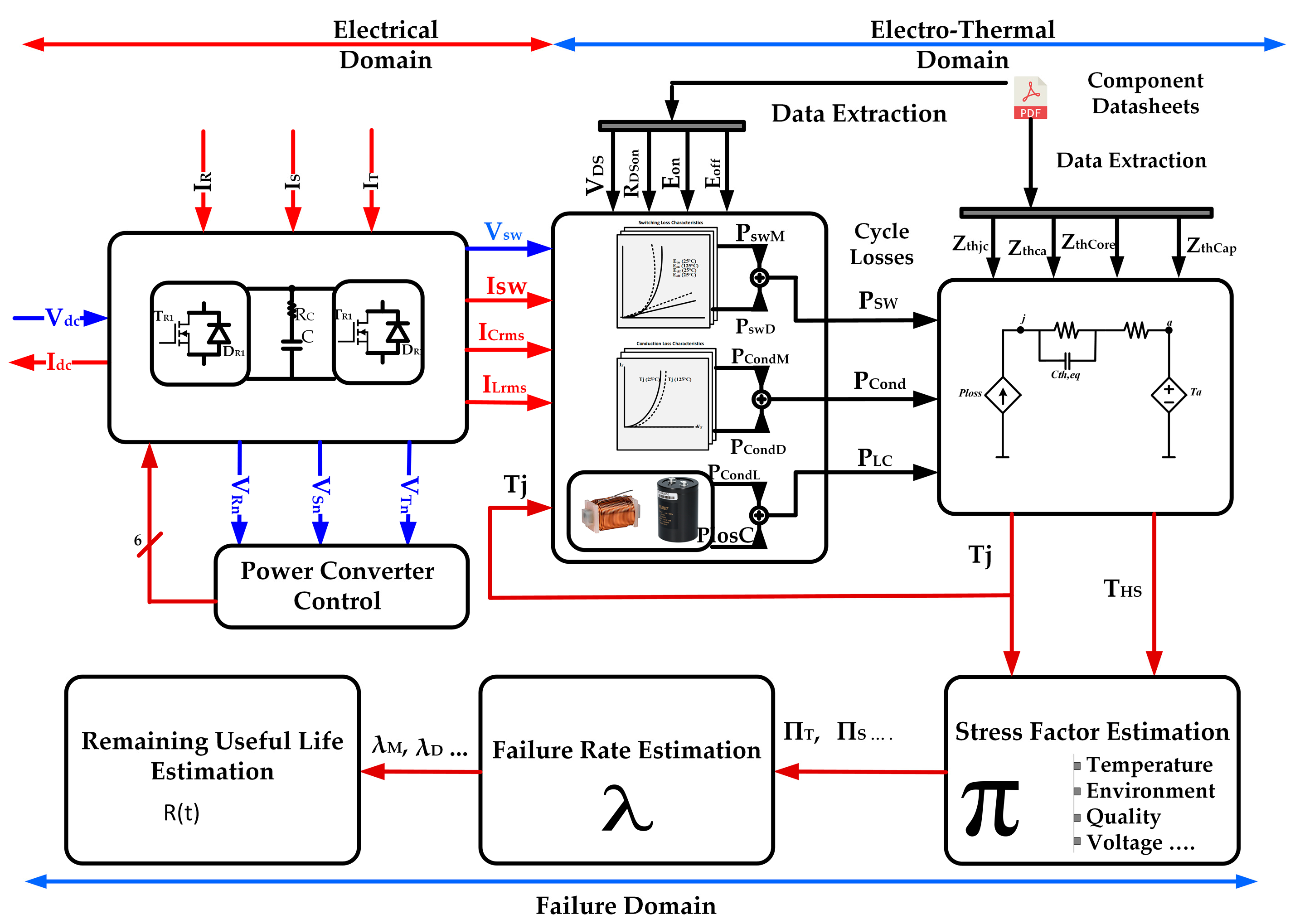
This section describes the PE interface degradation towards mean time to failure caused by stress factors generated in the converters. The PE interface lifetime degradation estimation of the two-stage power converter is illustrated in Figure 3. As seen in Figure 3, the approach is composed of three parts: the electrical domain, which comprises the power stage and control part; the electro-thermal domain, which considers losses and resulting temperatures; and the failure domain, which incorporates possible failure rates and part stress factors to enable the inspection of the useful lifetime of the two-stage PE interface. Of these three domains, the electro-thermal domain is of utmost importance for assessing the degradation of the most failure-prone components in the PE interface, namely switches and capacitors [29]. The previously discussed electrical domain modeling was followed by loss modeling, thermal modeling, and finally, failure modeling in the subsequent sections to evaluate the impact of variations on the system response.

4.1. Loss Modeling

Accurately estimating the loss incurred by the PE interface during operation is complex but important because of its influence on performance and reliability. The semiconductor switching loss behavioral model is adopted to more accurately assess performance [30].
Owing to the fact that driver losses account for a small share of the total power loss, the total loss incurred is modeled with conduction and switching losses. The MOSFET conduction and switching losses are formulated by Equations (31)–(34). Similarly, Equations (35)–(38) are applied for the diode. To capture the behavior within operational variations of voltage, current, on-state resistance, frequency, and junction temperature, the lookup table approach was utilized for the selected SiC MOSFET switch [31,32].
P c o n d   ( M ) =   f ( V d s ( t ) ,   I d s ( t ) )
V d s = f ( I d s ( t ) ,   T j ( t ) )  
P o n & o f f = ( E S w _ o n ( I d s ( k ) ,   T j ( k ) ) + E S w _ o f f ( I d s ( k ) ,   T j ( k ) ) ) f s w
P M   ( T ) = P c o n d   ( M ) + P o n & o f f
where P M   ( T ) represents the total losses of the MOSFET; P c o n d   ( M ) is the conduction losses; P o n & o f f is the sum of turn-on and turn-off losses; Vds is the on-state voltage; Ids is the current drain-source current through the MOSFET; and Tj represents the junction temperature.
P t o t   ( D ) = P c o n d   ( D ) + P r r  
V f = f ( I f ( t ) ,   T j ( t ) )
P c o n d   ( D ) = f ( V f ( t ) ,   I f ( t ) )
P r r = f s w · E r r ( V f , I f , T j )
where Prr represents the turn-off power losses; Vf is the forward voltage drops; If is the forward diode current; and Err is the reverse recovery energy.
Additionally, the inductor and capacitor losses can be formulated by Equations (39) and (40):
P c o n d   ( L )   = I L , r m s 2 R L
P l o s s   C = I C , r m s 2 E S R ( f )
where Irmsy is the average current through the inductor, capacitor; RL is the Litz wire resistance of the inductor; and ESR is the equivalent series resistance of the capacitor.

4.2. Thermal Modeling

To obtain a good estimation of the junction and case temperatures, thermal modeling is considered with three key aspects. Firstly, the device case temperature is a direct result of the total loss generated by the device. Secondly, the temperature of the device is subject to variations arising from losses. Lastly, the influence of changes in the ambient temperature is imperative to consider.
The thermal modeling approach for the PE interface is detailed in [33]. With the former aspects, the switch thermal model is formulated by Equations (41)–(44), the capacitor by Equation (45), and the inductor by Equations (46) and (47):
Z t h j c = R t h 1 τ t h 11 + 1 + R t h 2 τ t h 2 + 1 + + R t h n τ t h n + 1
τ t h = R t h C t h
T C = Δ T C A + T A
T j = Δ T J C + T C
where Z t h j c is the junction to case thermal resistance (°C/W), τ t h is the response time, Δ T C A is the case to ambient temperature change, T C is the case temperature, T j is the junction temperature, and R t h is the thermal resistance.
T H S ( C ) = T A + Δ T ( = P l o s s   R t h   )
T H S ( L ) = T A + 1.1 Δ T
Δ T = 125 P l o s s / A
where T H S ( C ) and T H S ( L ) are the hotspot temperatures of the inductor and capacitor, respectively, and A is the radiating surface area of the inductor.

4.3. Failure Modeling

The possible failure of the PE interface under the conditions of being in good and degraded states can be described with Equation (48), as per the Markov chain model [34]:
d d x [ P G ( t )     P D ( t ) ] = [ P G ( t )     P D ( t ) ] [ λ G D λ G D 0 0 ]
where P G denotes the possibility of normal operation with the components being in good state; P D denotes the possibility of being in a degraded state with a failure of any of the components; and λ G D is the failure rate while transitioning from good to degraded states.
Assuming the initial operating state as good, the operational reliability can be expressed by Equation (49):
R ( t ) = 1 P D ( t ) = P G ( t ) = e λ t
The failure rates of the two-stage converter are calculated using the parts stress method, as formulated by Equation (50) [35]:
λ G D = i = 1 n λ S w i + i = 1 n λ i n d i + i = 0 n λ D i + i = 0 n λ C a p i
where λD, λSw, λCap, λind, and n denote the failure rates of the diode, switch, capacitor, inductor, and the number of these components used, respectively. According to MIL-HDBK-217F [36], the failure rate of a device is affected by the quality of the components, the environment, contact construction, capacitance, and temperature.

5. Results and Discussion

The design of the passive components and the system requirements are presented in [37]. This work extends the design considering the electrical and control performances and regarding lifetime assessment with various switching frequencies for SiC power MOSFETs. The base case system specifications and parameters are shown in Table 1. The discussion of the performance of the various cases is presented in the following subsections.

5.1. Controller Performance

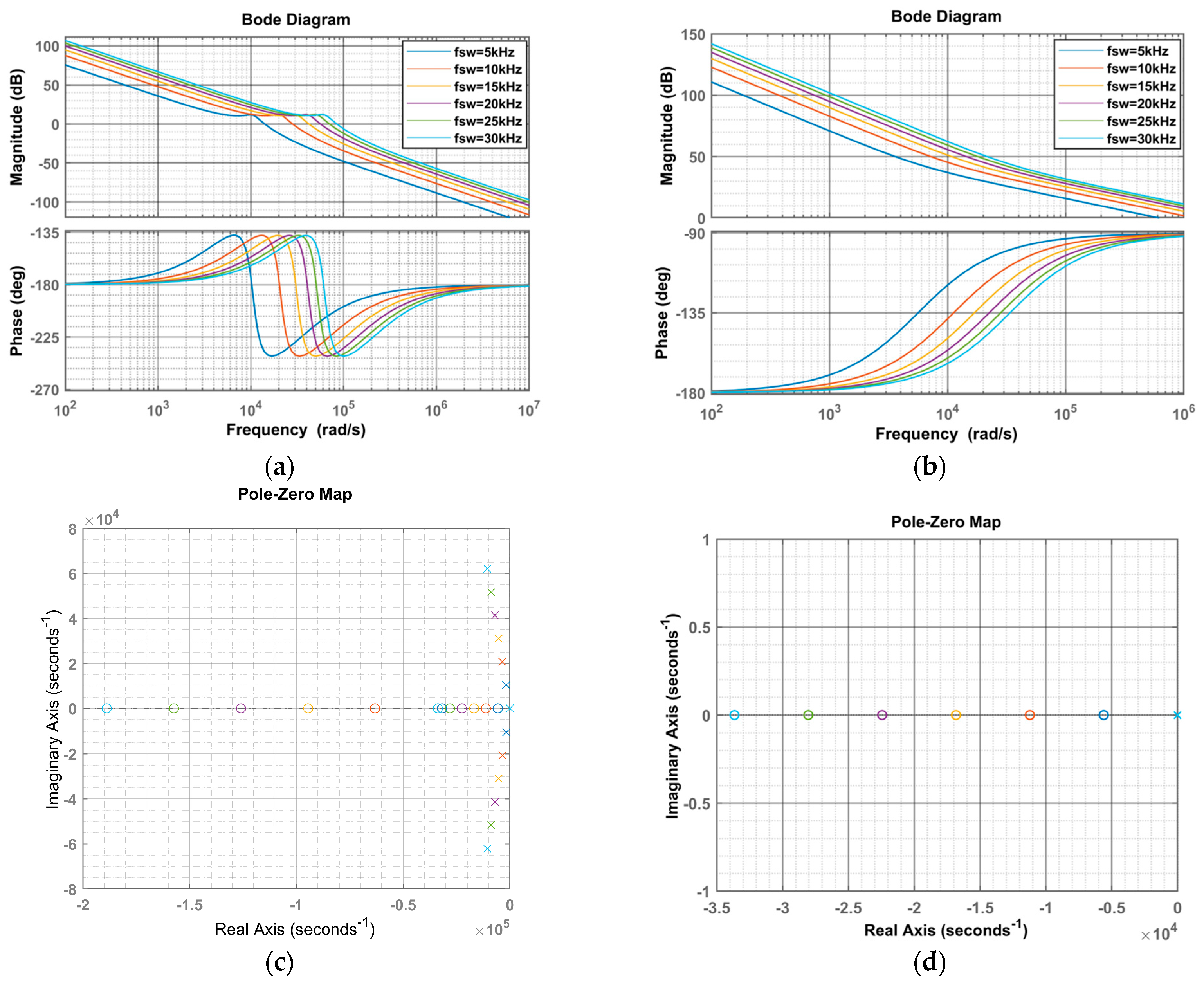
The analysis of the voltage and current loop stability for the AC/DC interface is shown in Figure 4 in a comparative view of varying switching frequency. The plant-transfer function for both loops is a function of induction and capacitance, which is affected by the switching frequency, thus leading to varied closed-loop system responses. The main objective was to improve the load transient response by varying the switching frequency. The load transient response was better at higher switching frequencies because the bandwidth of the controller could be increased.
The Bode plot regarding the current control loop shown in Figure 4a indicated that the resonance frequency shifted from 9 to 90 kHz within the selected switching frequency range of 5–30 kHz. However, the gain and phase margins for the current loop remained greater than 3 dB and 30°, respectively.
Similarly, the response of the voltage control loop shown in Figure 4b depicted a positive shift in gain and phase margins for the switching frequency range. Based on the figures, it could be concluded that both control loops remained in the stable region with the variation in switching frequency.
The stability of both control loops was further confirmed by the pole-zero map, as shown in Figure 4c,d. These figures demonstrated that the poles remained in the left half of the plane, even with the variation in frequency.
The analysis procedure for the DC/DC interface at the battery side was similar to the former and the performance of both control loops is shown in Figure 5a,b. It was noted in these figures that the gain margin varied from 30 to 75 dB for both control loops within the switching frequency range of 5 to 30 kHz. Furthermore, it was observed that the magnitude of the plot maintained a 30 dB per decade characteristic. The phase margin was within the range of 45° to 70° for the given switching frequency range. These corresponding gain and phase margin ranges were utilized to calculate the controller gain for the voltage and current loops of the DC/DC stage for the system response assessment.
Moreover, the pole-zero map for the voltage-current loop of the DC/DC converter is depicted in Figure 5c,d. The placement of the poles in the left half of the plane ensured the stability of the system.
However, in order to examine the system response and settling time for the DC/DC converter current and voltage controllers, as an example, the unit step response of the studied switching frequency was analyzed. Figure 6a,b illustrates the unit step response for the current controller, demonstrating that the settling time decreased proportionally from 2.5 to 0.3 ms for the current control loop and from 7 to 1 µs for the voltage control loop for the 5 to 30 kHz switching frequency variation.

5.2. System Performance

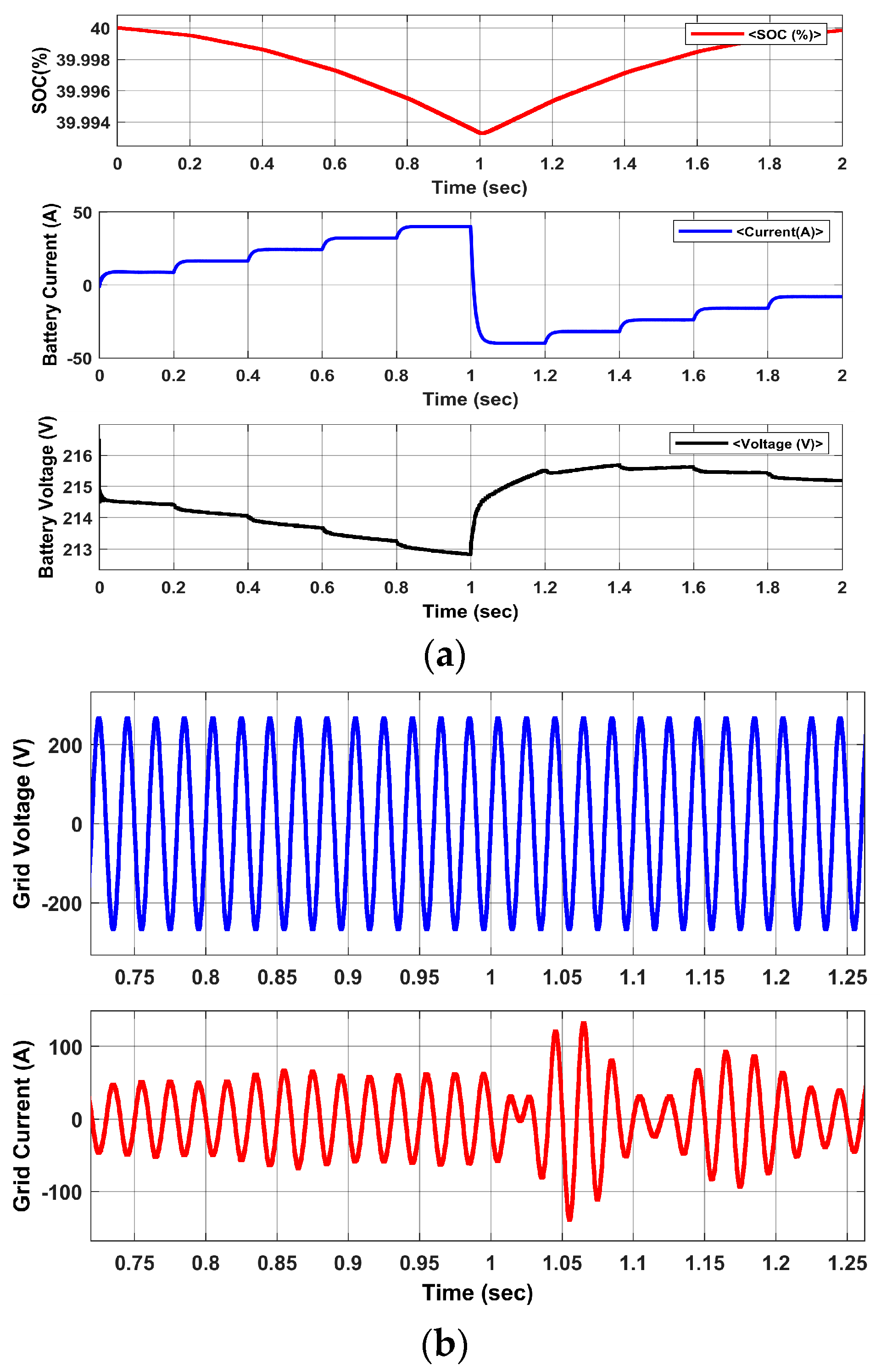
The simulation outcomes of the battery pack-interfaced converter in the charging and discharging modes are depicted in Figure 7a. The converter’s power was negative from time t = 0 s to time t = 1 s, which meant that the battery was discharging based on the requested power with voltage and current, accordingly. The requested power range varied from 2 to 10 kW up to 1 s simulation time. During this time, the SoC decreased at different rates. Moreover, the battery voltage decreased from 214.5 to 213 V. The voltage and current in the AC side are also shown in Figure 7b.
Conversely, between the time periods of t = 1 s and t = 2 s, charging power was requested, indicating that the battery system consumed the DC current and was being charged. It was observed that the battery voltage exhibited a high increment rate at 10 kW of requested power, reaching its maximum voltage during charging at a power consumption of 8 kW at t = 1.4 s. In addition, the amount of grid current was consumed in the range of 45 A–55 A (peak) with a total harmonic distortion (THD) of 1.6%.
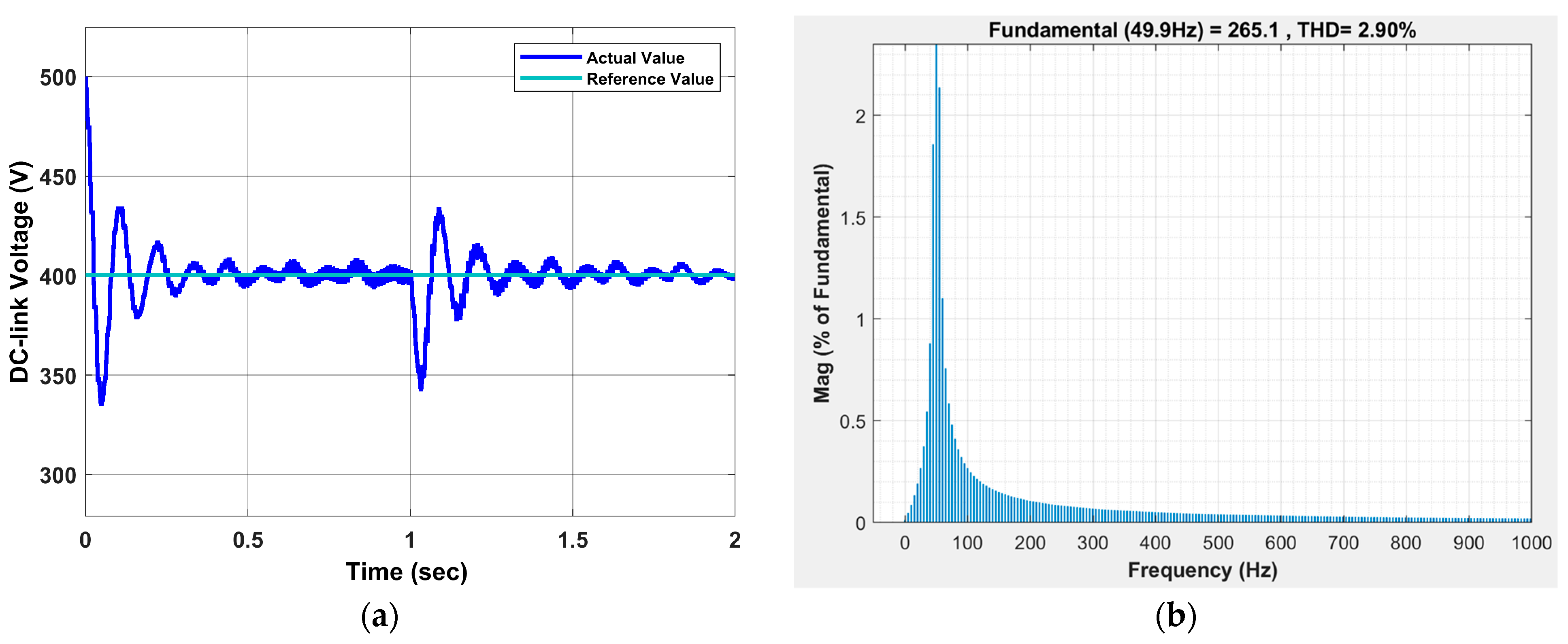
The DC-link voltage profile is depicted in Figure 8a. The DC-link voltage fluctuation was more frequent due to changes in the requested power for both modes of operation. Specifically, the voltage ripple was around 1% (4 V) during the steady state period for each requested power. However, the fluctuation was around 25% (100 V) during the power transferring mode transition. It was clearly observed that the voltage controller maintained the DC-link voltage during charging and discharging with the desired voltage ripple. The amount of grid current in the range of 48–60 A (peak) was injected to the grid with 2.9% THD during the discharging period, as shown in Figure 8b. However, the THD varied up to 4% for the 10 to 30 kHz switching frequency variation.

5.3. Evaluation of Losses

The simulation outcomes of the two-stage converter losses are discussed in this section. The voltage and current stress on the Q1 switch of the first leg was not uniform for the charging and discharging modes. Thus, the switching losses in the same leg were different for the AC/DC and DC/DC power stages for both modes of operation. The switching losses occurred due to the switching current cycle when the device was turned on.
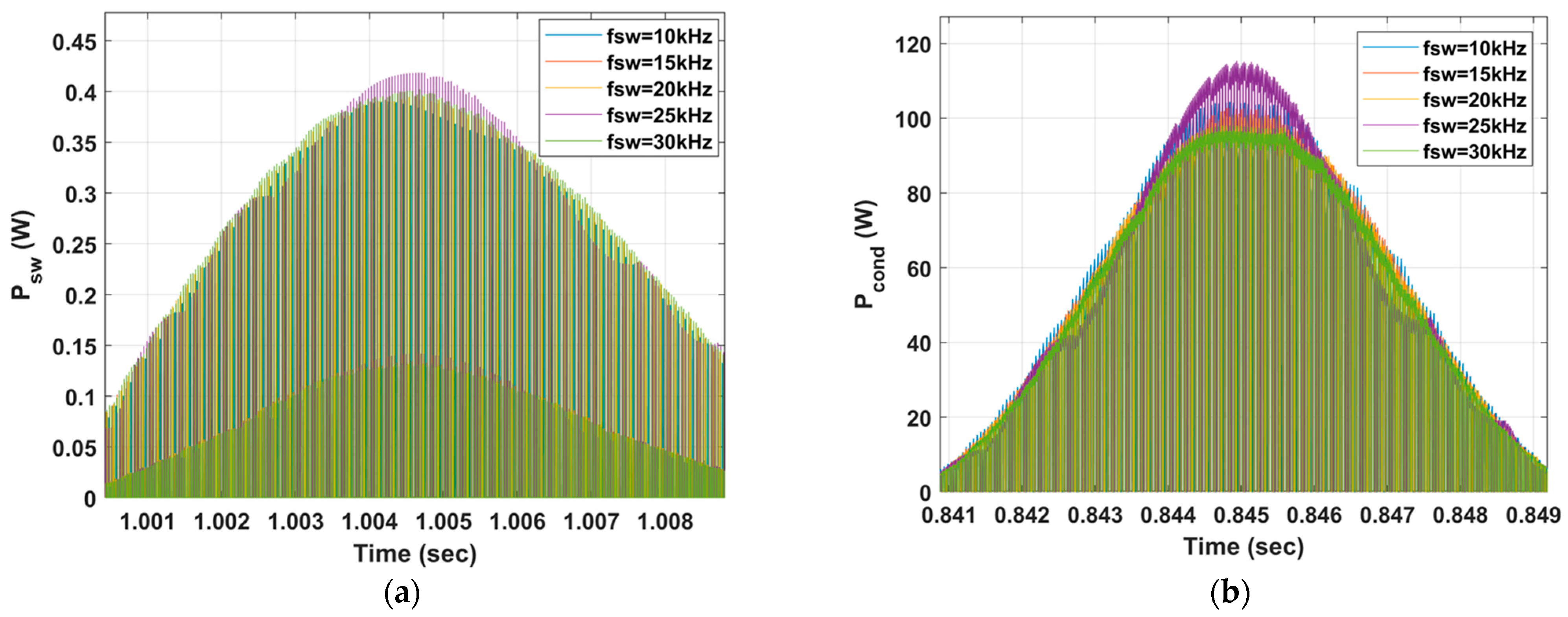
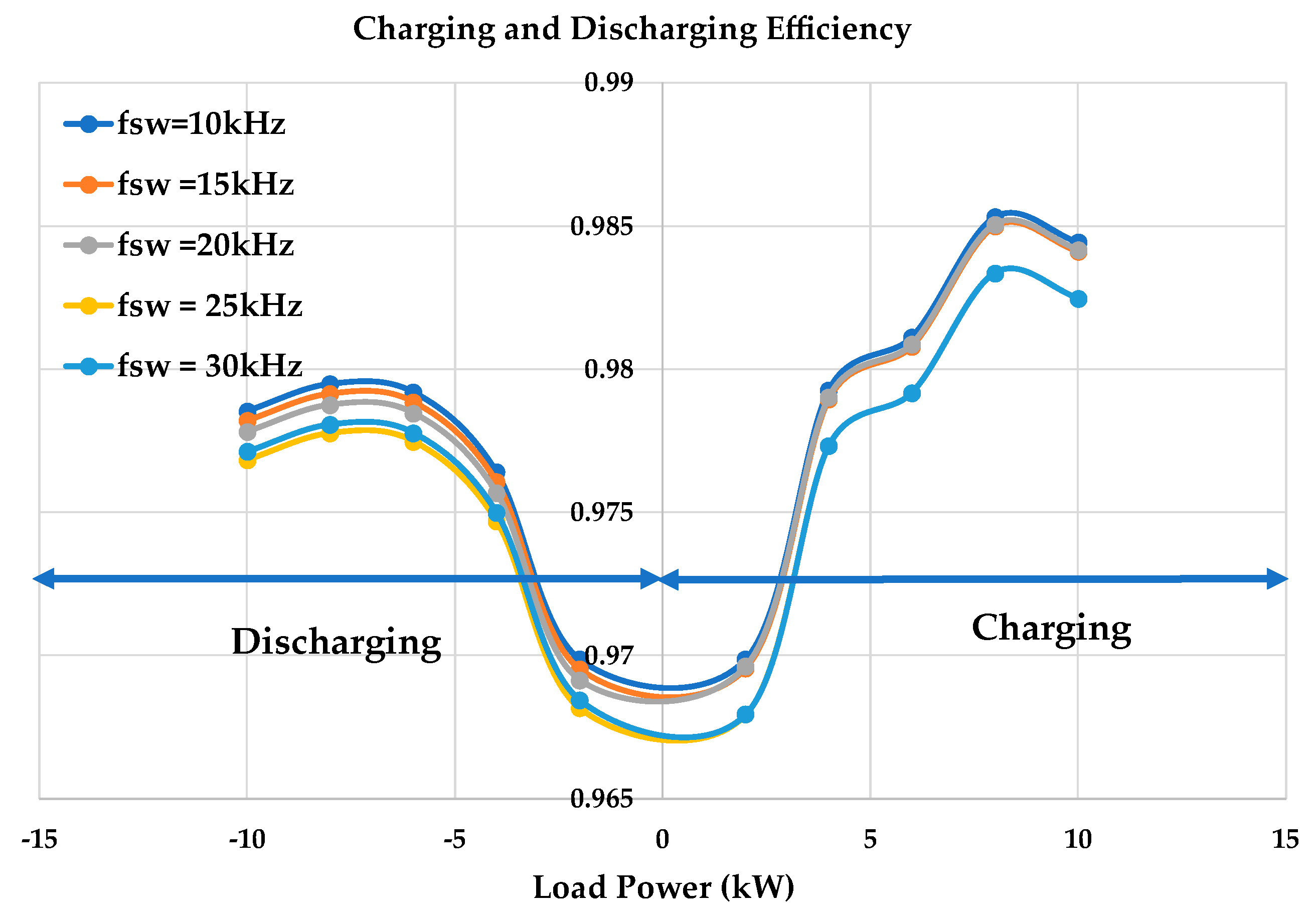
From Figure 9a, it was observed that the switching losses for the Q1 MOSFET varied up to 0.4 W for the given switching frequency range during 10 kW discharging operation for the AC/DC converter. On the other hand, the conduction losses shown in Figure 9b for the MOSFET were around 120 W. In this assessment work, the switching and conduction losses for the SiC MOSFET switch used in the two-stage bidirectional converter were considered. Therefore, the efficiency map was different at different switching frequencies. The efficiency map in different switching frequencies is depicted in Figure 10. The maximum efficiencies were around 97.8% (discharging) and 98.6% (charging) at 8 kW load power.

5.4. Degradation Assessment

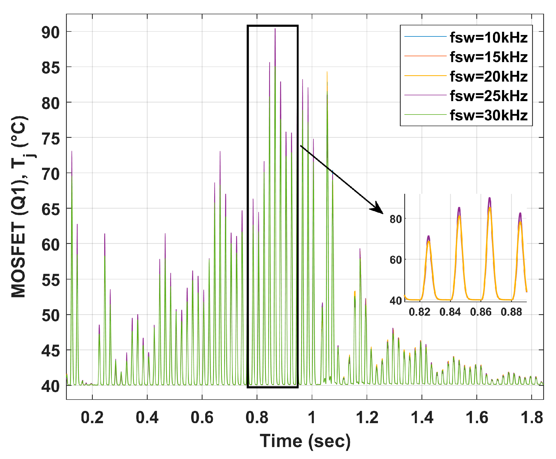
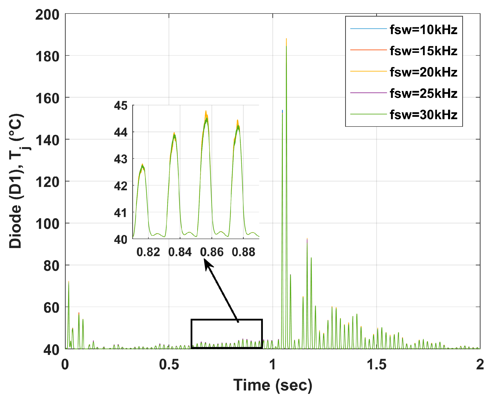
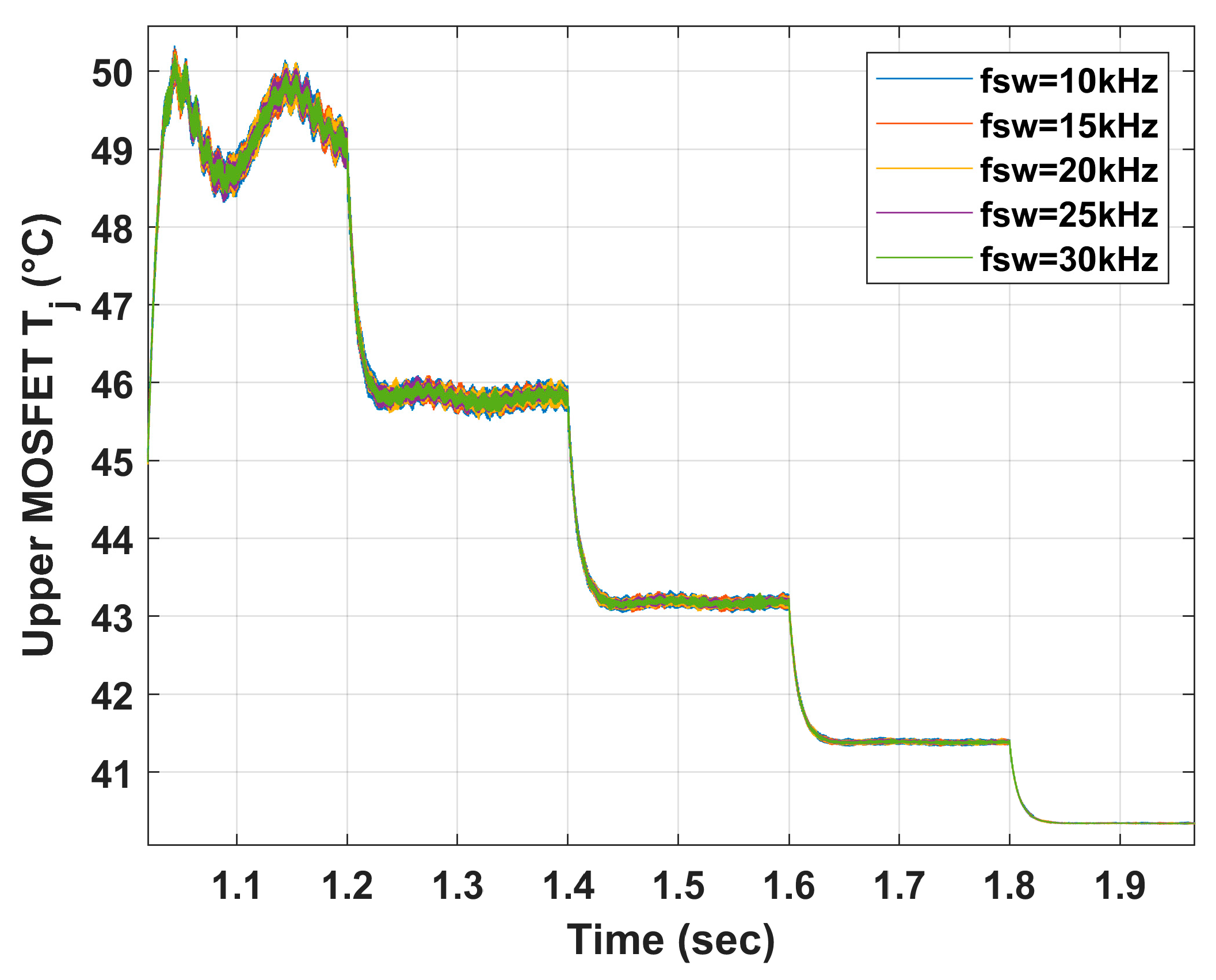
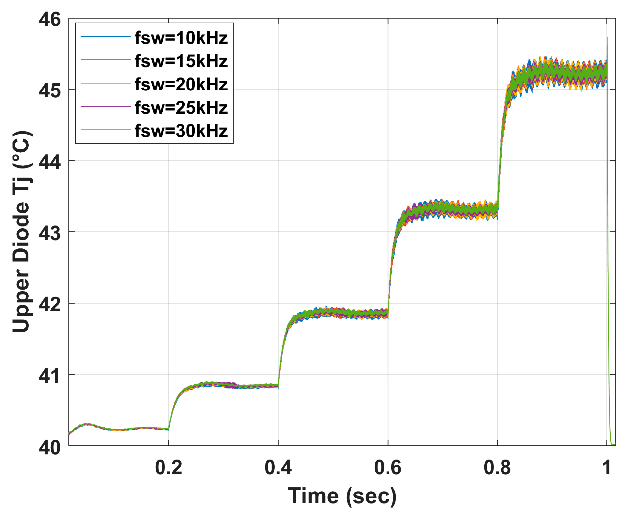
The degradation assessment was initiated with the measurement of different stress estimations. Different stress factors usually affect the power converter. Thermal cycling stress is most significant for assessing the degradation of power semiconductor switches. The junction temperature profiles of the upper MOSFET(Q1) switch and diode are shown in Figure 11 and Figure 12, respectively. These figures showed that the thermal cycling impact was most significant on the MOSFET switch compared to the diode during the discharging operation. Moreover, ∆Tj was approximately 20–50 °C for the MOSFET switch whereas it was below 5 °C for the diode during the discharging operation of the AC/DC converter for the switching frequency variation of 5–30 kHz).
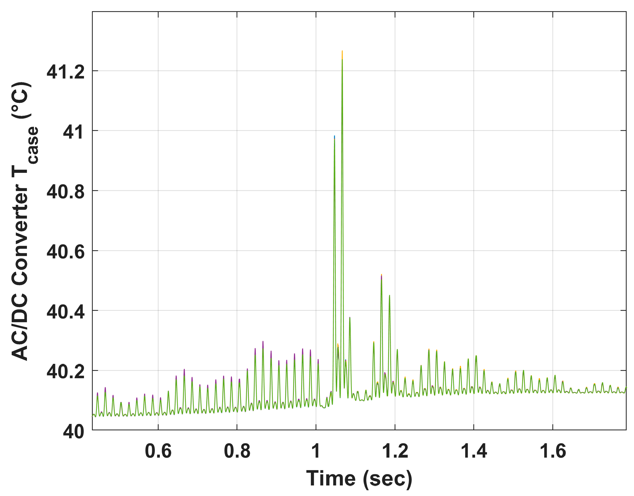
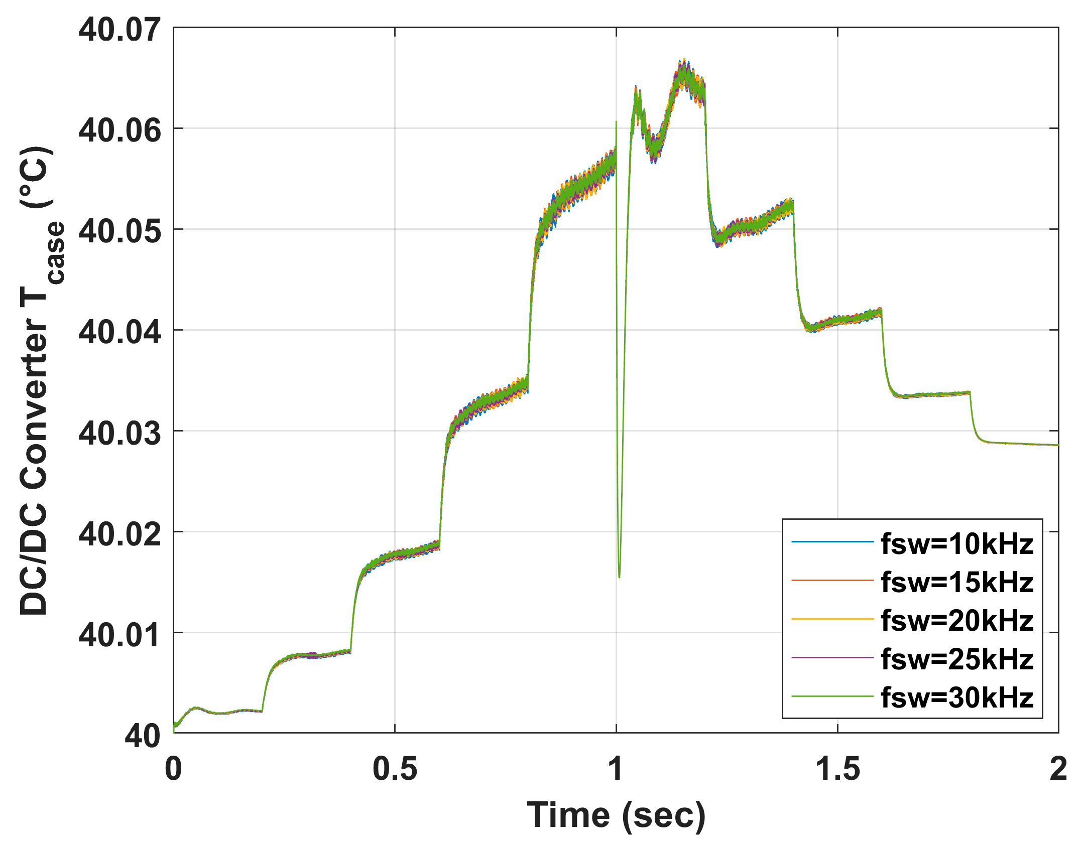
For the DC/DC converter, ∆Tj was very low (<1 °C) due to the unidirectional PWM signal. During the discharge operation, the upper diode temperature was estimated around 45 °C on average with 0.3 °C ∆Tj, whereas the MOSFET achieved a temperature of around 49 °C with 0.5 °C ∆Tj variation, as shown in Figure 13 and Figure 14. During the operations of charging and discharging, the thermal cycling for all semiconductor switches contributed to the case temperature profile. From Figure 15 and Figure 16, it was observed that the average case temperature increased over time. This indicated that the losses occurring over time were adding heat to the power converter case.
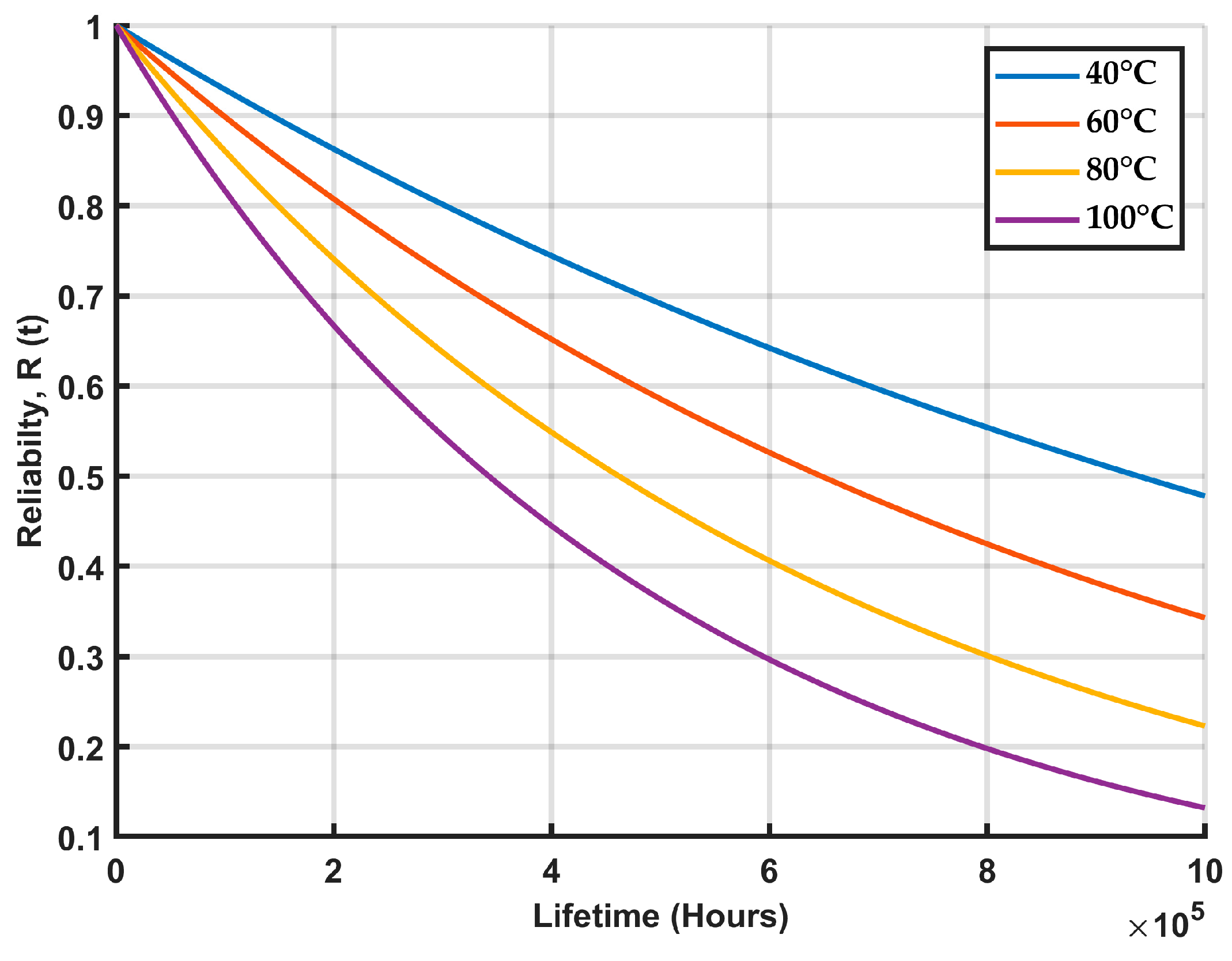
As previously discussed, the operating switching frequency of a semiconductor device can significantly impact the case temperature profile. Higher switching frequencies allow for an increase in the speed at which electrons move through the material, leading to increased heat dissipation and a corresponding rise in temperature. If the temperature rises too high, electronic components may malfunction or fail, posing a significant reliability issue. The degradation of the two-stage converter reliability is demonstrated in Figure 17, which highlights that the PE system was more reliable when operating at lower temperatures. Specifically, if the selected operating switching frequency maintained the PE converter’s operating temperature at around 60 °C, the PE system could operate reliably for 98,900 h (approximately 10 years) with a 90% reliability rate. In contrast, if the operating temperature exceeded 100 °C, the PE system’s lifetime would degrade to five years (49,700 h). Thus, careful consideration of the operating temperature and switching frequency is necessary to optimize the reliability and lifespan of a PE system.

6. Conclusions

In this work, a comprehensive performance assessment of a two-stage power electronic (PE) converter for interfacing the grid of a lithium-ion battery energy storage system in BIPV applications has been presented. The control strategy for the AC/DC and DC/DC converters was assessed for a given 5–30 kHz switching frequency range, and the voltage and current loops’ robustness was analyzed using Bode plots and pole-zero mapping. It was observed that the poles for the voltage and current loops for both converters were in the left half of the plane for the complex domain up to 30 kHz switching frequency.
It was also further observed that increasing the switching frequency by the same amount offered diminishing returns in terms of reduction in settling time. For example, increasing the switching frequency from 10 to 15 kHz reduced the settling time by 34.6%, whereas increasing the switching frequency from 20 to 25 kHz only reduced the settling time by 23.1%. To obtain a balanced trade-off between a responsive PE converter and to reduce loss, a switching frequency of 10 kHz was selected.
The system’s electrical performance was also presented, indicating that the DC-link voltage ripple was lower than 2% in the stable region for the charging and discharging operations within the given switching frequency range. Moreover, the grid current THD was around 2.9% during the discharging operation, indicating that the controller allowed for good-quality power injection by the battery energy storage system through the power converter.
Moreover, the overall electro-thermal performance was summarized by assessing the efficiency map for the charging and discharging operations. It was observed that the discharging efficiency was 0.5% lower than the charging efficiency. This phenomenon showed that the power stage faced significant losses during the discharging operation. Additionally, the lifetime was analyzed by considering the component-level stress factors. The system lifetime was estimated to be 10 years, with a system-level reliability of 90%. The MOSFET lifetime was mostly affected by the diode during the discharging operation.
Finally, this work provides valuable insight into the performance assessment of a two-stage bidirectional PE for PV–BESS system application. However, the study’s innovation lies in its assessment of the impact of regulating different switching frequencies at partial- to full-load operation. The results presented in this study can aid in the design and development of efficient and robust power converters for BIPV applications.

Author Contributions

Methodology, M.M.H., S.J., and T.G.; software, M.M.H. and S.J.; writing—original draft preparation, M.M.H.; writing—review and editing, S.J., T.G., and O.H.; supervision, T.G. and O.H. All authors have read and agreed to the published version of the manuscript.

Funding

This project has received funding from the European Union’s Horizon 2020 research and innovation program under grant agreement No. 963527 (iSTORMY). Energies 16 04486 i001

Data Availability Statement

Not applicable.

Acknowledgments

This project has received funding from the European Union’s Horizon 2020 research and innovation program under grant agreement No. 963527 (iSTORMY). The authors also acknowledge and appreciate the Flanders Make for their support to the MOBI research group.

Conflicts of Interest

The authors declare no conflict of interest.

References

  1. Chalamala, B. Energy Storage and the Electric Grid—Stabilizing the Renewable Energy Dominated Utility Grid Through Storage; No. SAND2020-13574C; Sandia National Lab. (SNL-NM): Albuquerque, NM, USA, 2020. [Google Scholar]
  2. Building Integrated Photovoltaics—BIPV Status Report 2020—News—BIPV Boost. Available online: https://bipvboost.eu/news-and-events/news/building-integrated-photovoltaics-bipv-status-report-2020/ (accessed on 24 January 2023).
  3. International Energy Agency. Innovation in Batteries and Electricity Storage, September 2020. Available online: https://iea.blob.core.windows.net/assets/77b25f20-397e-4c2f-8538-741734f6c5c3/battery_study_en.pdf (accessed on 1 March 2023).
  4. Lithium-Ion Battery Market for Stationary Applications—Global Industry Analysis, Size, Share, Growth, Trends, and Forecast, 2020–2030. Transparency Market Research, May 2021. Available online: https://www.transparencymarketresearch.com/lithium-ion-battery-market-for-stationary-application.html (accessed on 1 March 2023).
  5. Townsend, A.; Gouws, R. A Comparative Review of Lead-Acid, Lithium-Ion and Ultra-Capacitor Technologies and Their Degradation Mechanisms. Energies 2022, 15, 4930. [Google Scholar] [CrossRef]
  6. Yudhistira, R.; Khatiwada, D.; Sanchez, F. A comparative life cycle assessment of lithium-ion and lead-acid batteries for grid energy storage. J. Clean. Prod. 2022, 358, 131999. [Google Scholar] [CrossRef]
  7. Institute of Electrical and Electronics Engineers. IEEE Standard for Interconnecting Distributed Resources with Electric Power Systems; IEEE: Piscataway, NJ, USA, 2003. [Google Scholar]
  8. Hyeon, L.J.; Yoon, Y.H.; Kim, J.M. Analysis of IEC 61727 Photovoltaic (PV) Systems Characteristics of the Utility Interface. Int. J. Internet Broadcast. Commun. 2015, 7, 90–95. [Google Scholar] [CrossRef]
  9. Turksoy, A.; Teke, A.; Alkaya, A. A comprehensive overview of the dc-dc converter-based battery charge balancing methods in electric vehicles. Renew. Sustain. Energy Rev. 2020, 133, 110274. [Google Scholar] [CrossRef]
  10. Blaabjerg, F.; Ma, K.; Zhou, D. Power electronics and reliability in renewable energy systems. In Proceedings of the 2012 IEEE International Symposium on Industrial Electronics, Hangzhou, China, 28–31 May 2012; pp. 19–30. [Google Scholar] [CrossRef] [Green Version]
  11. Nandi, R.; Tripathy, M.; Gupta, C.P. Coordination of BESS and PV system with bidirectional power control strategy in AC microgrid. Sustain. Energy Grids Netw. 2023, 34, 101029. [Google Scholar] [CrossRef]
  12. Yang, Y.; Zhou, K.; Blaabjerg, F. Current Harmonics From Single-Phase Grid-Connected Inverters—Examination and Suppression. IEEE J. Emerg. Sel. Top. Power Electron. 2015, 4, 221–233. [Google Scholar] [CrossRef] [Green Version]
  13. Zakzouk, N.E.; Abdelsalam, A.K.; Helal, A.A.; Williams, B.W. High Performance Single-Phase Single-Stage Grid-Tied PV Current Source Inverter Using Cascaded Harmonic Compensators. Energies 2020, 13, 380. [Google Scholar] [CrossRef] [Green Version]
  14. Chatterjee, A.; Mohanty, K.B. Current control strategies for single phase grid integrated inverters for photovoltaic applications-a review. Renew. Sustain. Energy Rev. 2018, 92, 554–569. [Google Scholar] [CrossRef]
  15. Rocabert, J.; Luna, A.; Blaabjerg, F.; Rodríguez, P. Control of Power Converters in AC Microgrids. IEEE Trans. Power Electron. 2012, 27, 4734–4749. [Google Scholar] [CrossRef]
  16. Chauhan, S.; Singh, B. Control of solar PV-integrated battery energy storage system for rural area application. IET Renew. Power Gener. 2021, 15, 1030–1045. [Google Scholar] [CrossRef]
  17. Erfani, M.J.; Thiringer, T.; Haghbin, S. Performance and losses analysis of charging and discharging mode of a bidirectional DC/DC fullbridge converter using PWM switching pattern. In Proceedings of the 2011 IEEE Vehicle Power and Propulsion Conference, Chicago, IL, USA, 6–9 September 2011; pp. 1–6. [Google Scholar] [CrossRef]
  18. Karanki, S.B.; Xu, D. Voltage droop control of dual active bridge for integrating battery energy storage to utility gird. In Proceedings of the 2014 IEEE Energy Conversion Congress and Exposition (ECCE), Pittsburgh, PA, USA, 15—18 September 2014; pp. 2227–2232. [Google Scholar] [CrossRef]
  19. Bakeer, A.; Chub, A.; Shen, Y.; Sangwongwanich, A. Reliability analysis of battery energy storage system for various stationary applications. J. Energy Storage 2022, 50, 104217. [Google Scholar] [CrossRef]
  20. Radionova, L.; Chernyshev, A. Mathematical Description of AFE Rectifier Closed Loop System. Procedia Eng. 2015, 129, 16–21. [Google Scholar] [CrossRef] [Green Version]
  21. Qian, K.; Gao, G.; Sheng, Z. A Maximum Current Control Method for Three-Phase PWM Rectifier for the ITER In-Vessel Vertical Stability Coil Power Supply. IEEE Trans. Plasma Sci. 2018, 46, 1689–1693. [Google Scholar] [CrossRef]
  22. Li, W.; Ruan, X.; Pan, D.; Wang, X. Full-Feedforward Schemes of Grid Voltages for a Three-Phase LCL-Type Grid-Connected Inverter. IEEE Trans. Ind. Electron. 2013, 60, 2237–2250. [Google Scholar] [CrossRef]
  23. Tao, Z.; Li, L. Control loop design and bidirectional control strategy of a bidirectional DC/DC converter. In Proceedings of the IECON 2017—43rd Annual Conference of the IEEE Industrial Electronics Society, Beijing, China, 29 October–1 November 2017; pp. 5720–5725. [Google Scholar] [CrossRef]
  24. AlZawaideh, A.; Boiko, I. Analysis of a Sliding Mode DC–DC Boost Converter through LPRS of a Nonlinear Plant. IEEE Trans. Power Electron. 2020, 35, 12321–12331. [Google Scholar] [CrossRef]
  25. Saldaña, G.; Martín, J.I.S.; Zamora, I.; Asensio, F.J.; Oñederra, O. Analysis of the Current Electric Battery Models for Electric Vehicle Simulation. Energies 2019, 12, 2750. [Google Scholar] [CrossRef] [Green Version]
  26. Rajanna, B.V.; Kumar, M.K. Chopper-Based Control Circuit for BESS Integration in Solar PV Grids. Energies 2021, 14, 1530. [Google Scholar] [CrossRef]
  27. Bae, J.-Y. Electrical Modeling and Impedance Spectra of Lithium-Ion Batteries and Supercapacitors. Batteries 2023, 9, 160. [Google Scholar] [CrossRef]
  28. MathWorks. Battery (Power System Toolbox); MathWorks: Natick, MA, USA, 2021; Available online: https://www.mathworks.com/help/sps/powersys/ref/battery.html (accessed on 12 March 2023).
  29. GopiReddy, L.R.; Tolbert, L.M.; Ozpineci, B. Power Cycle Testing of Power Switches: A Literature Survey. IEEE Trans. Power Electron. 2014, 30, 2465–2473. [Google Scholar] [CrossRef]
  30. Ivanovic, Z.; Blanusa, B.; Knezic, M. Power loss model for efficiency improvement of boost converter. In Proceedings of the 2011 XXIII International Symposium on Information, Communication and Automation Technologies, Sarajevo, Bosnia and Herzegovina, 27–29 October 2011; pp. 1–6. [Google Scholar] [CrossRef]
  31. Torsaeter, B.N.; Tiwari, S.; Lund, R.; Midtgard, O.-M. Experimental evaluation of switching characteristics, switching losses and snubber design for a full SiC half-bridge power module. In Proceedings of the 2016 IEEE 7th International Symposium on Power Electronics for Distributed Generation Systems (PEDG), Vancouver, BC, Canada, 27–30 June 2016; pp. 1–8. [Google Scholar] [CrossRef]
  32. Cree Inc. C3M0016120D Datasheet. Wolfspeed, December 2020. Available online: https://assets.wolfspeed.com/uploads/2020/12/C3M0016120D.pdf (accessed on 12 March 2023).
  33. Sintamarean, C.; Blaabjerg, F.; Wang, H. A novel electro-thermal model for wide bandgap semiconductor based devices. In Proceedings of the 2013 15th European Conference on Power Electronics and Applications (EPE), Lille, France, 2–6 September 2013; pp. 1–10. [Google Scholar] [CrossRef] [Green Version]
  34. Ye, Y.; Grossmann, I.E.; Pinto, J.M.; Ramaswamy, S. Modeling for reliability optimization of system design and maintenance based on Markov chain theory. Comput. Chem. Eng. 2019, 124, 381–404. [Google Scholar] [CrossRef]
  35. Aghdam, F.H.; Abapour, M. Reliability and Cost Analysis of Multistage Boost Converters Connected to PV Panels. IEEE J. Photovoltaics 2016, 6, 981–989. [Google Scholar] [CrossRef]
  36. USA Department of Defense. Military Handbook MIL HDBK 217F: Reliability Prediction of Electronic Equipment. Washington, USA, December 1991. Available online: http://snebulos.mit.edu/projects/reference/MIL-STD/MIL-HDBK-217F-Notice2.pdf (accessed on 12 March 2023).
  37. Hasan, M.; Jaman, S.; Geury, T.; Hegazy, O. Design and Simulation of a Grid-Connected Two-Stage Bidirectional Converter for a Combined PV-Stationary Energy Storage System. In Proceedings of the 2022 Second International Conference on Sustainable Mobility Applications, Renewables and Technology (SMART), Cassino, Italy, 23–25 November 2022; pp. 1–8. [Google Scholar] [CrossRef]
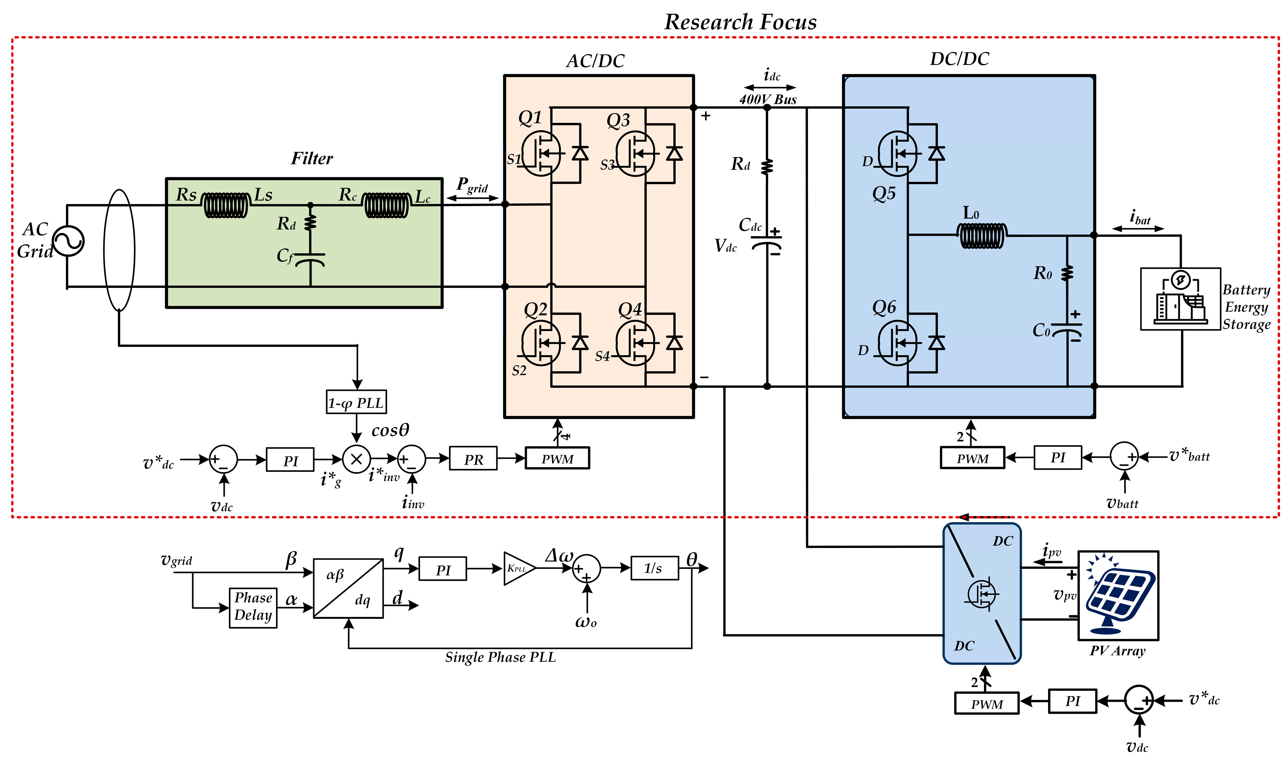
Figure 1. Conceptual system architecture with grid-interfaced battery energy storage system where “*” represents the reference value of the corresponding parameters (battery voltage, vbatt; grid current, ig; inverter current, iinv).
Energies 16 04486 g001
Figure 2. Generic battery model based on dynamic charge and discharge behavior.
Energies 16 04486 g002
Figure 3. Lifetime estimation approach for the PE interface of the PV combined with BESS.
Energies 16 04486 g003
Figure 4. Control performance of AC/DC interface: (a) Bode plot of current controller; (b) Bode plot of voltage controller; (c) Pole-zero map of current control; (d) Pole-zero map of voltage control. Where ”o” and “×” notify the position of the closed-loop zeros and poles, respectively.
Energies 16 04486 g004
Figure 5. Control loop performance of DC/DC converter: (a) Bode diagram of current control; (b) Bode diagram of voltage control; (c) pole-zero map of current control; (d) pole-zero map of voltage control. Where “o” and “×” signify the position of the closed-loop zeros and poles, respectively.
Energies 16 04486 g005
Figure 6. Comparative step response of the converter with different switching frequencies: (a) current control loop for DC/DC; (b) voltage control loop for DC/DC.
Energies 16 04486 g006
Figure 7. Electrical performance during charging and discharging modes: (a) battery side; (b) grid side.
Energies 16 04486 g007
Figure 8. Electrical performance: (a) DC-link voltage profile during bidirectional power flow; (b) THD for discharging mode.
Energies 16 04486 g008
Figure 9. Upper side of SiC power MOSFET loss distribution of AC/DC: (a) switching losses; (b) conduction losses.
Energies 16 04486 g009
Figure 10. Efficiency map of the two-stage power converter during charging and discharging operations from 10 to 30 kHz switching frequency.
Energies 16 04486 g010
Figure 11. Junction temperature for MOSFET switch (upper side) for AC/DC converter.
Energies 16 04486 g011
Figure 12. Junction temperature for diode (upper side) for AC/DC converter.
Energies 16 04486 g012
Figure 13. Junction temperature for MOSFET switch (upper side) for DC/DC converter during charging.
Energies 16 04486 g013
Figure 14. Junction temperature for diode (upper side) for DC/DC converter during discharging.
Energies 16 04486 g014
Figure 15. Case temperature of AC/DC converter.
Energies 16 04486 g015
Figure 16. Case temperature of DC/DC converter.
Energies 16 04486 g016
Figure 17. Failure probability of operating lifetime with different operating temperatures.
Energies 16 04486 g017
Table 1. System specifications with designed passive components.
ParametersValueParametersValue
Energy storage Battery capacity50 kWhFilter Inductance (Grid Side)0.813 mH
Maximum Output Power10 kWFilter Capacitance30 uF
Battery Nominal Voltage200 VFilter Inductance (Converter Side)0.867 mH
Rated Capacity50 AhESR+Damping resistance10 Ω
Charging/Discharging rate2 COutput filter Inductance4.06 mH
Charge/discharge current at 1 C22 AOutput Filter Capacitance500 uF
Rated AC Input Voltage,
frequency
230 V, 50 HzSwitching
Frequency
10 kHz
Disclaimer/Publisher’s Note: The statements, opinions and data contained in all publications are solely those of the individual author(s) and contributor(s) and not of MDPI and/or the editor(s). MDPI and/or the editor(s) disclaim responsibility for any injury to people or property resulting from any ideas, methods, instructions or products referred to in the content.