Article

Power Interference Suppression Method for Measuring Partial Discharges under Pulse Square Voltage Conditions

Key Laboratory of Engineering Dielectrics and Its Application, Ministry of Education, School of Electrical and Electronics Engineering, Harbin University of Science and Technology, Harbin 150080, China
*
Author to whom correspondence should be addressed.
Energies 2022, 15(9), 3437; https://doi.org/10.3390/en15093437
Submission received: 21 March 2022 / Revised: 2 May 2022 / Accepted: 6 May 2022 / Published: 8 May 2022
(This article belongs to the Section F6: High Voltage)

Abstract

:
Partial discharge (PD) is an important metric for the insulation diagnosis of power equipment. However, its detection is affected by the strong electromagnetic interference generated by pulse square voltage. We therefore propose a power interference suppression method for partial discharges under pulse square voltage based on a quadratic measurement method. We conduct analysis of the topology circuit when partial discharge occurs in the insulation test sample and introduce the basic principle of the secondary measurement method according to the superposition principle and the linear relationship between the square voltages at different peak values. We verify the feasibility of this method by simulating a PD signal with power interference. Subsequently, we use the successive interception comparison method to solve the non-correspondence of the two initial measurement points problem and design and manufacture the transformer turn-to-turn oil-paper insulation test sample and experimental tank. By measuring the PD starting voltage of the insulation test sample under the power frequency voltage, we determined the first measurement voltage under the pulse square voltage and obtained the signal x1(t) to subsequently measure the PD signal x2(t). According to the proposed successive interception comparison method, the signal x1(t) is processed, and the secondary measurement method suppresses the power interference of the measured signal x2(t). We demonstrate that the proposed method effectively suppresses the power interference in PD detection under a pulse square voltage.

Graphical Abstract

1. Introduction

Owing to the frequent action of circuit breakers, power electronic devices and other switching equipment, power equipment is affected by high-frequency pulse overvoltage [1,2,3,4]. High-frequency pulse overvoltage is characterised by high frequency, steepness and a short rise time. The pulse square voltage is a typical high-frequency pulse overvoltage [5,6,7]. Partial discharge, which refers to an electrical discharge that does not completely bridge the space between two conducting electrodes, occurs in the insulation of power equipment under a pulse square wave voltage. It is one of the main reasons for insulation damage, and it is also an effective means of evaluating and diagnosing the insulation state of power equipment [8,9,10]. Under the action of the pulse square voltage, the partial discharge signal detection is affected by the strong electromagnetic interference generated by the power supply [11,12,13]. The partial discharge signal is submerged in the power interference signal. Therefore, to accurately evaluate the insulation state of power equipment, it is of great significance to effectively suppress the power interference and extract the partial discharge signal.
Correlation studies were conducted on the technology related to partial discharge measurement under a high-frequency pulse voltage. A dual-mode conical horn antenna was designed. It is used to measure high-frequency partial discharge pulse signals, and a test system of partial discharge under pulse square voltage was designed [14]. A high-frequency current transformer (HFCT) was used to detect partial discharge signals under high-frequency pulse voltage [15]. The dynamic sensor is characterised by a wide working frequency band with the ability to operate in high-frequency environments and have high response sensitivity; however, its ability to suppress power interference is not ideal. A SiC partial discharge test platform under a 10 kV square wave voltage pulse was built [16]. The partial discharge was measured by the antenna, and the power interference was filtered by a high-pass filter. The high-pass filter can better suppress the power interference; however, it is limited by overfiltering and underfiltering. The partial discharge under square voltage in the ultrahigh frequency range was measured in [17,18], and the electromagnetic wave generated by the partial discharge was detected by the antenna; the measurement frequency band of this method is limited. A balance circuit was then proposed [19]; two experimental samples are needed to build the balance circuit and ensure that the partial discharge initial voltages of the two experimental samples are sufficiently different. When there is no partial discharge in the two experimental samples, the bridge equilibrium is adjusted. When the voltage rises, one experimental sample undergoes partial discharge, and the other does not. At this time, the differential amplifier has an output, and the output signal is the partial discharge signal generated in the experimental sample. This method can effectively suppress the interference caused by the power supply. However, it is difficult to adjust the bridge balance; moreover, it is necessary to ensure that the two samples cannot discharge simultaneously.
When the pulse square voltage is applied on the insulation, due to the short rise and fall time of the voltage at the rising edge and the falling edge, the space charge in the defect of the insulation is less than rotation. The direction of the electric field generated by the space charge is the same as the direction of the applied electric field, which enhances the electric field at the insulation defect and makes the defect more prone to partial discharge. When the applied voltage is at the flat top (positive and negative half cycle), the electric field generated by the space charge at the defect is opposite to the external electric field, which weakens the electric field at the insulation defect and inhibits the partial discharge at the flat top. Therefore, under the action of pulse square voltage, partial discharge mainly occurs at the rising edge and falling edge of pulse square voltage. Because the rising edge and falling edge of the pulse square voltage change very fast, reaching tens of nanoseconds, it makes the time domain characteristics of the pulse voltage interference generated by the pulse square voltage source in the rising edge and falling edge very similar to the time domain characteristics of the partial discharge. The two are aliasing. It is difficult to suppress the interference generated by the pulse square voltage source by using the different frequency characteristics of interference signal and partial discharge signal. On the other hand, although the balance circuit method can suppress the interference of pulse square power supply, its shortcomings make it difficult to achieve in reality.
To solve the shortcomings of power interference suppression in the aforementioned partial discharge (PD) detection process, this paper proposes a power interference suppression method for measuring partial discharge under pulse square voltage based on the secondary measurement method. The process of simulating the partial discharge signal is detailed in Section 2; four typical partial discharge simulation signals under different frequencies were simulated using MATLAB software. Section 3 introduces the basic principle of the secondary measurement method through circuit analysis of partial discharge under pulse square voltage and verifies the effectiveness of the secondary measurement method through simulation analysis. In Section 4, the first measurement data are processed by the successive interception comparison method to determine the correspondence point between the first and second measurement data and to solve the problem of time difference between the two measurements data. In Section 5, the experimental scheme is determined; moreover, we discuss the design and manufacture of the oil-paper insulation between the turns of the transformer and the experimental oil tank. Based on the secondary measurement method, power interference suppression of the experimental data was carried out. Finally, our conclusions are summarised in Section 6. Through simulation and measurement, this method can effectively suppress power interference in partial discharge signal detection under a pulse square wave voltage.

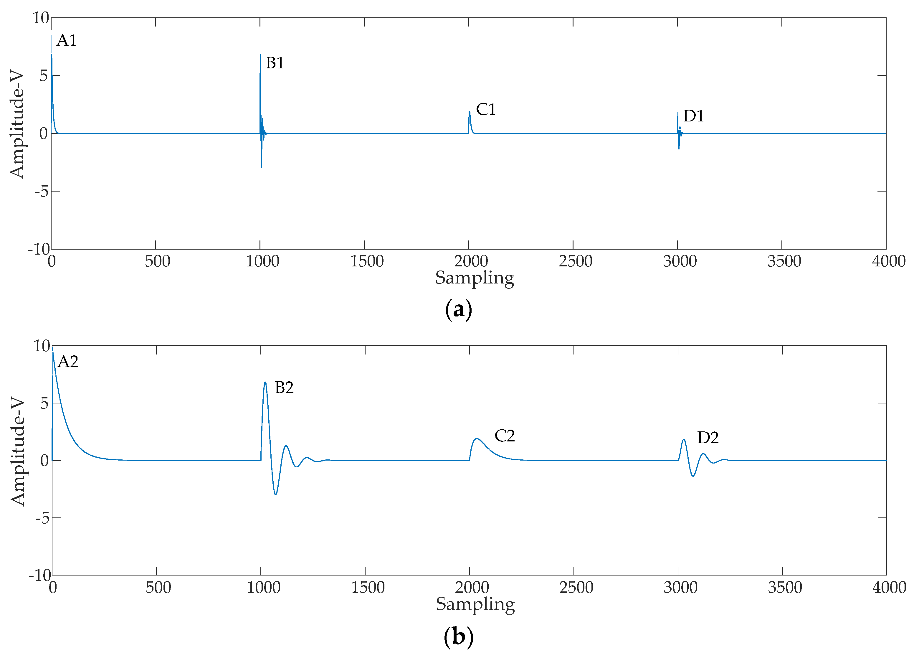
2. PD Signal for Simulation Analysis

The PD signal is a type of pulse signal with a fast-rising edge; it indicates many discharge types and has a short discharge time [20,21,22,23,24]. PD simulation signals can generally be represented by four mathematical models [25,26,27,28,29]: single-exponential decay model D1, single-exponential decay oscillation model D2, double-exponential decay model D3 and double-exponential decay oscillation model D4. The specific expressions are as follows:
D 1 = { A 1 e ( t t 0 ) / τ t t 0 0 t < t 0
D 2 = { A 2 e ( t t 0 ) / τ sin [ 2 π f c ( t t 0 ) ] 0 t t 0 t < t 0
D 3 = { A 3 ( e 1.3 ( t t 0 ) / τ e 2.2 ( t t 0 ) / τ ) 0 t t 0 t < t 0
D 4 = { A 4 [ e 1.3 ( t t 0 ) / τ e 2.2 ( t t 0 ) / τ ] sin [ 2 π f c ( t t 0 ) ] 0 t t 0 t < t 0
In Equations (1)–(4), A1, A2, A3 and A4 are the PD simulation signal amplitudes, τ is the attenuation coefficient, fc is the attenuation oscillation frequency, t is the duration of the PD signal pulse, and t0 is the time of partial discharge [30,31,32].
In this study, MATLAB simulation software (version 2017, MathWorks, Natick, MA, USA) was used to simulate two groups of partial discharge signals with different frequencies, y1(t) and y2(t). The parameters are listed in Table 1. A1 and A2 are single exponential decays, B1 and B2 are single exponential decay oscillations, C1 and C2 are double exponential decays and D1 and D2 are double exponential decay oscillations. The sampling frequency was 20 M samples/s, the sampling time was 200 μs and the number of sampling points was 4000. The PD simulation signal is shown in Figure 1.

3. Analysis of Power Interference Suppression

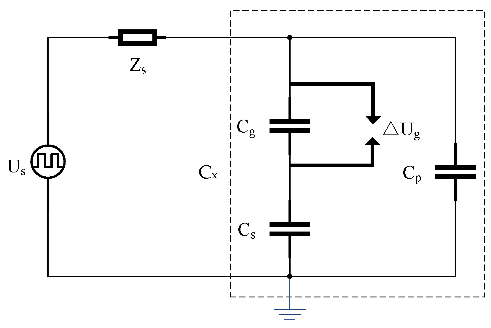
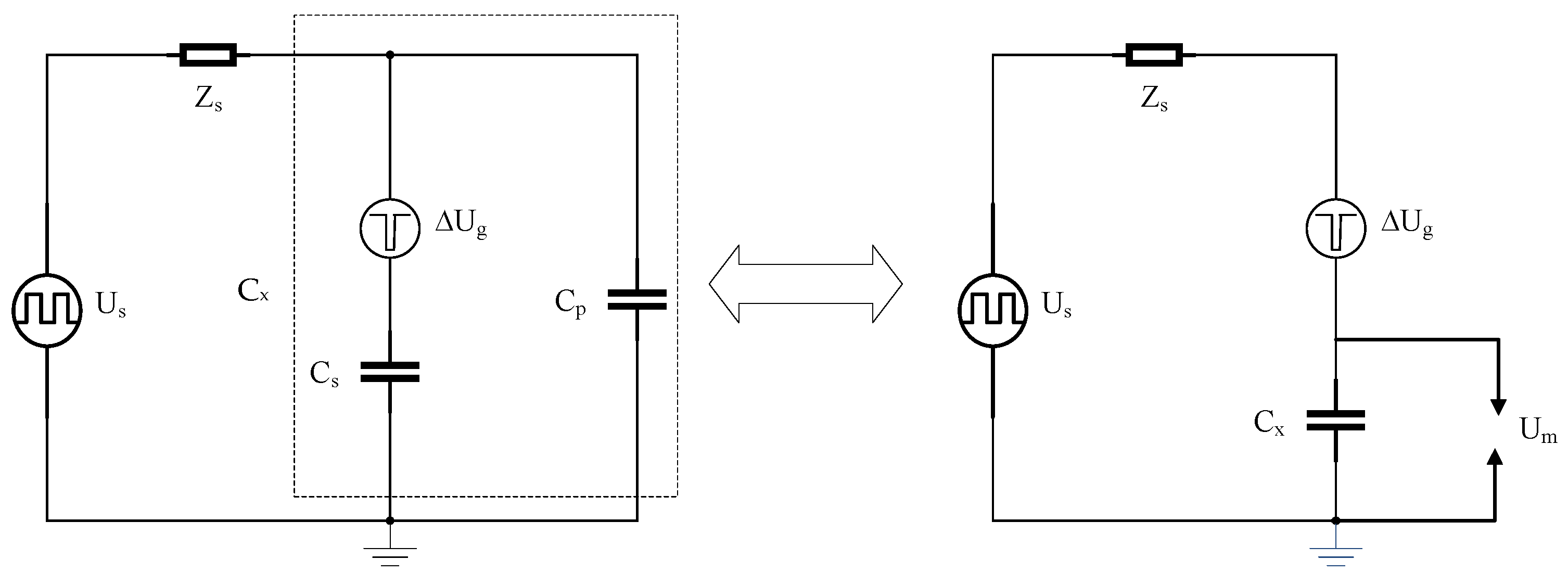
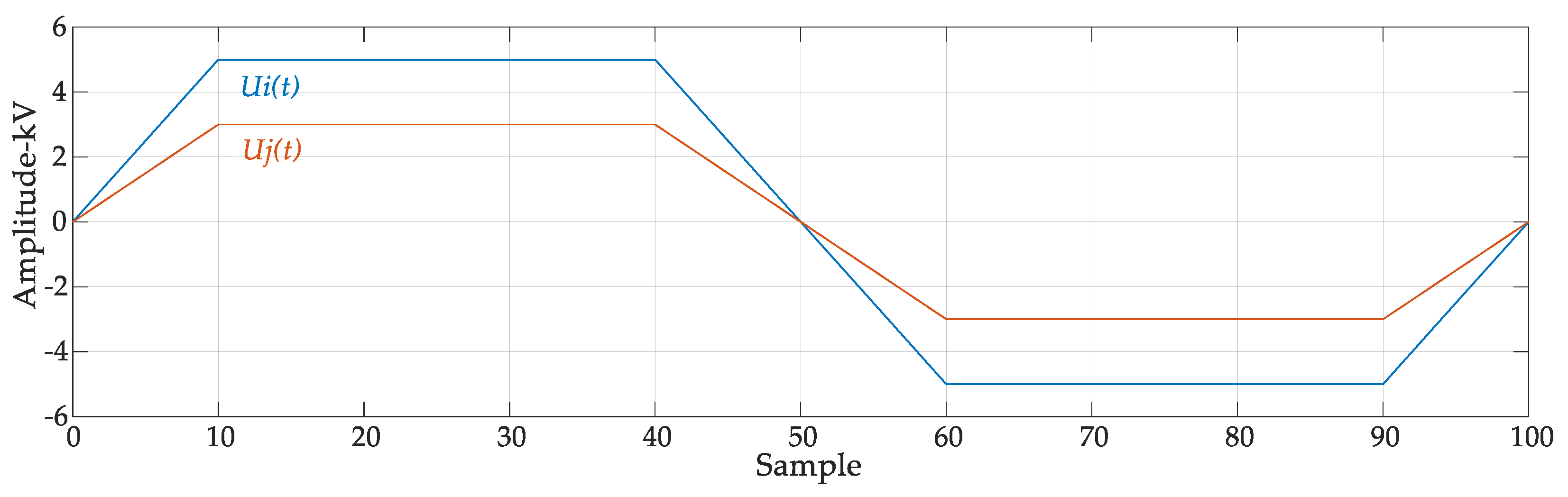
3.1. Circuit Analysis

The circuit diagram when pulse square voltage is applied to the insulation sample is shown in Figure 2. In the figure, Us is the pulse square voltage source, Zs is the protection resistance, Cx is the insulation sample and g is the defect in the insulation sample Cx.
When the pulse square voltage applied to the insulation sample Cx is lower than the partial discharge initial voltage of Cx, the equivalent circuit is shown in Figure 3. In the figure, Cg is the equivalent capacitance at the defect, Cs is the equivalent capacitance of part s and Cp is the equivalent capacitance of part p.
When partial discharge occurs at the defect in Cx a weak pulse voltage ΔUg is generated at the defect, and the equivalent circuit is shown in Figure 4.
According to the superposition principle [33,34], when partial discharge occurs on Cx, the voltage Um at Cx equals the voltage U1 generated at Cx when Us acts alone on Cx, and the voltage U2 generated by the partial discharge pulse voltage ΔUg acts alone on the insulation sample Cx, namely Um = U1 + U2; the equivalent circuit diagram is shown in Figure 5.
In the partial discharge measurement, the actual pulse voltage ΔUg generated by partial discharge cannot be accurately measured; only the voltage U1 generated by the pulse voltage ΔUg acting on the insulation sample Cx can be measured, i.e., the apparent partial discharge voltage. Because the frequency of the pulse square voltage is high and the rise rate is large, the amplitude of voltage U1 generated by the partial discharge is much smaller than that of the pulse square voltage; hence, the power interference U2 has a serious impact on the measurement of the partial discharge. Therefore, it is necessary to suppress the influence of the power interference. The process of removing the interference of the pulse square voltage power supply involves removing U2 from the measured signal Um.

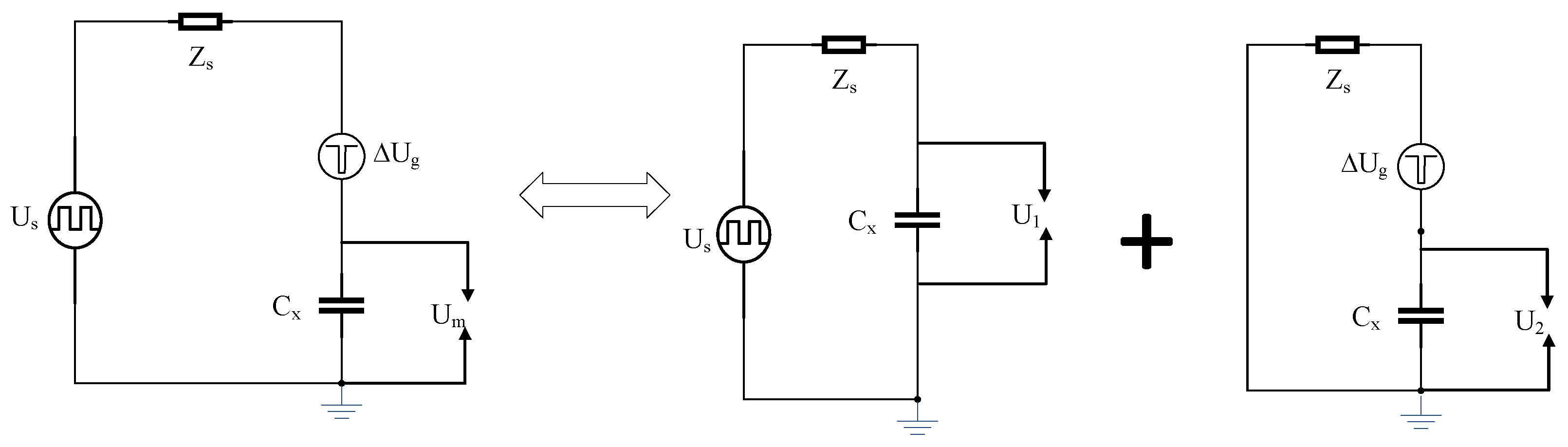
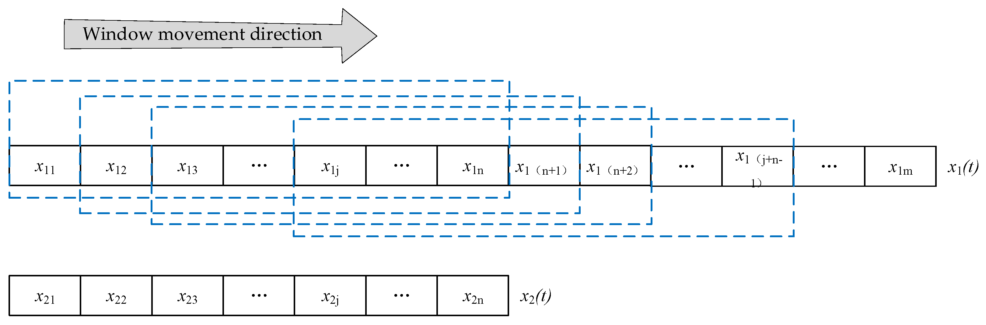
3.2. Basic Principle of Power Interference Suppression

There is a linear relationship among the pulse square voltages with the same parameters (frequency, voltage rise time and duty ratio) but different peak values. If the peak value of the pulse square voltage is Ai = aAj (where a is a constant), then Ui(t) = aUj(t). In Figure 6, the peak values are Ai = 5 kV and Aj = 3 kV, the frequency is fci = fcj = 10 kHz, the voltage rise time is tri = trj = 1 μs and the duty cycle is dri = drj = 50%. To facilitate observation, the sampling rate is 1 M samples/s, the sampling time is 100 μs and the number of sampling points is 100.
When pulse square voltages with the same parameters but different amplitudes act on the insulation sample Cx, the voltage generated on the insulation sample Cx also has a linear relationship. The partial discharge initial voltage of the insulation test sample Cx is Us, and the pulse square voltage on the insulation test Cx is U3. If U3 < Us, the partial discharge does not occur in the insulation test Cx; that is, the measured signal U3(t) does not contain the partial discharge signal. According to the linear relationship between U3(t) and U1(t), U1(t) can be obtained as shown in Equation (5). U1(t) can be calculated by measuring U3(t) to remove the power interference in the process of obtaining the partial discharge measurement under a pulse square voltage. Finally, the power interference in the partial-discharge detection signal is suppressed under the pulse square voltage.
U 1 ( t ) = U 1 U 3 U 3 ( t )
In summary, the partial discharge signal can be obtained through the signals U3(t) and Um(t) obtained by two measurement signals: one with no partial discharge and one with partial discharge. Thus, the power interference in the partial discharge measurement process under a pulse square voltage can be removed. The calculation process is given in Equation (6).
U 2 ( t ) = U m ( t ) U 1 ( t ) = U m ( t ) U 1 U 3 U 3 ( t )

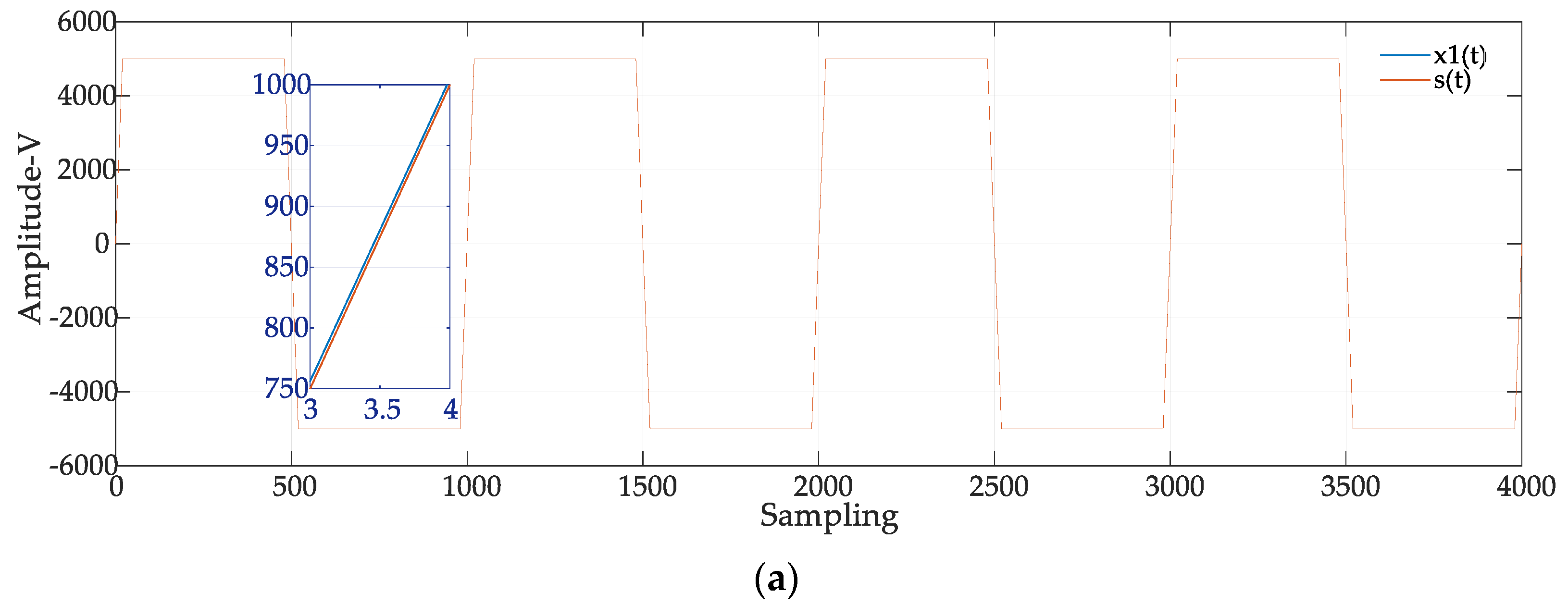
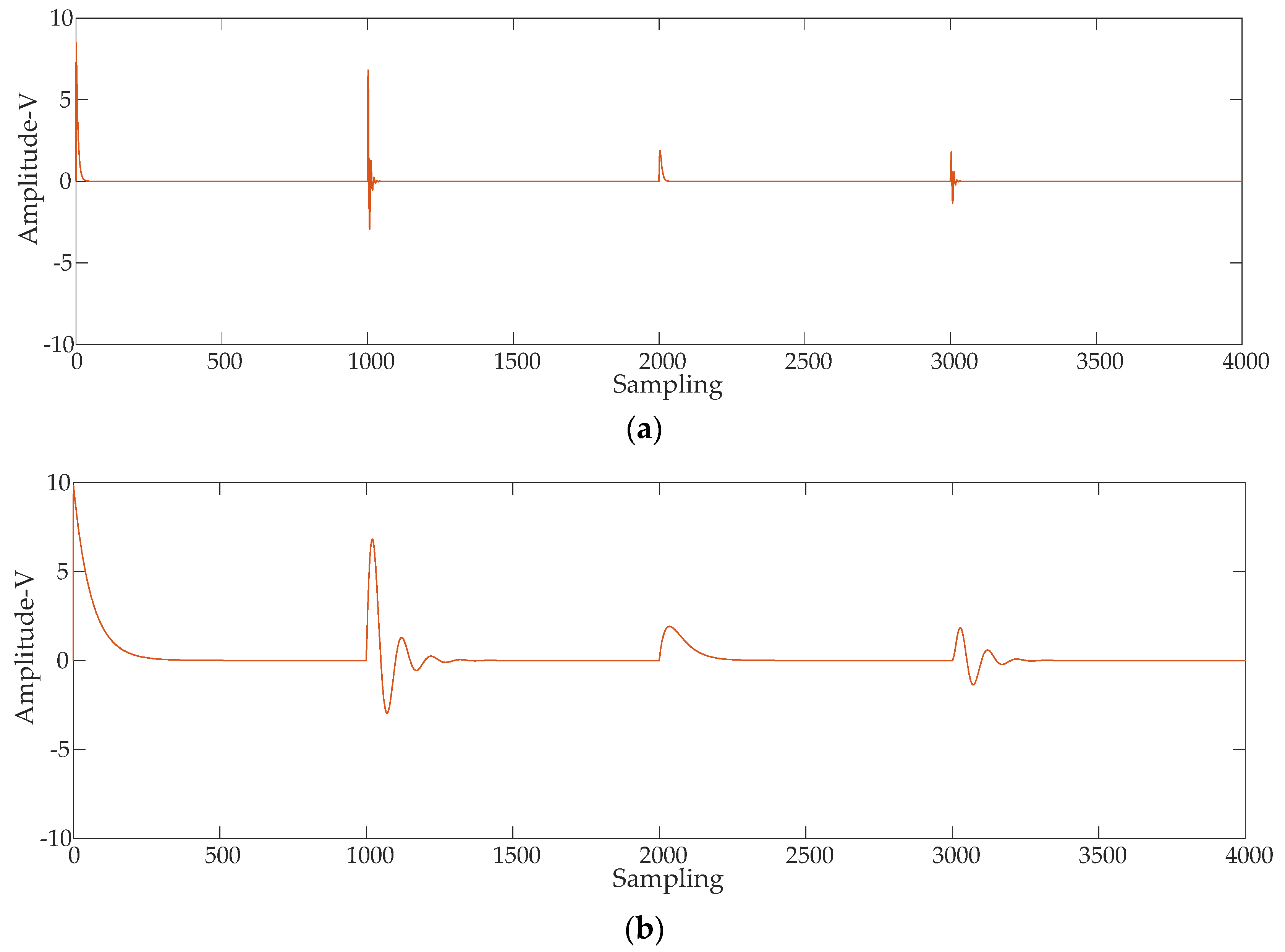
3.3. Simulation Analysis

The pulse square wave voltage is characterised by high frequency, large rise rate (DV/DT) and short rise time [35,36,37]. The pulse square wave voltage waveform simulated using MATLAB is shown in Figure 7. In the figure, the pulse square wave voltage frequency is 20 kHz, the voltage amplitude is 5 kV and the voltage rise time is 1 μs. The duty cycle was 50%, the sampling rate was 20 M samples/s and the sampling time was 200 μs. The number of sampling points was 4000.
When the pulse square voltage is applied to the insulation sample Cx, because the rising/falling time of the voltage at the rising/falling edge is very short, the space charge in the insulation defect has no time to rotate, and the direction of the electric field generated by the space charge is the same as that of the applied electric field. This enhances the electric field at the insulation defect point, making the defect more prone to partial discharge. When the applied voltage is at the flat top (positive and negative half cycle), the electric field generated by the space charge at the defect is opposite to the direction of the external electric field, which weakens the electric field at the insulation defect and inhibits the partial discharge at the flat top. Therefore, under the action of the pulse square voltage, the partial discharge is mainly concentrated at the rising/falling edge. The simulated waveform of the partial discharge signal at the rising edge under the pulse square voltage is shown in Figure 8. In Figure 8a, x1(t) is the pulse square voltage superimposed PD simulation signals when fc = 2 MHz and τ = 0.3 μs, and s(t) is pulse square voltage. In Figure 8b, x2(t) is the pulse square voltage superimposed PD simulation signals when fc = 0.2 MHz and τ = 3 μs, and s(t) is pulse square voltage. It can be seen from Figure 8 that the PD signal is completely submerged in the power interference signal. In order to facilitate observation, the waveform in the figure is locally amplified.
As shown in Figure 8, the partial discharge signal is completely submerged in the power interference signal, and the partial discharge waveform cannot be identified. It is assumed that when the peak value of the pulse square voltage is 2 kV, there is no partial discharge in the insulation sample Cx. According to Equation (6), the data in Figure 8a,b is used to suppress the interference of the partial discharge power supply under the pulse square voltage. The obtained waveform is shown in Figure 9.
It can be seen from Figure 9 that the interference caused by the pulse square power supply can be effectively suppressed. To quantitatively measure the power interference suppression effect, this study introduces the normalised correlation coefficient (NCC) as the evaluation index; the calculation formula is shown in Equation (7), x(i) is the PD signal, and y(i) is the signal after interference suppression. By setting NCC = 1, it can be seen from the calculation results that if there is a good linear relationship among the pulse square voltage signals with different amplitudes, the power interference method proposed in this paper is effective under the pulse square voltage effect.
N C C = i = 1 N x ( i ) y ( i ) ( i = 1 N x 2 ( i ) ) ( i = 1 N y 2 ( i ) )

4. Measurement of Time Difference and Solution

To suppress the power interference while obtaining the partial discharge measurement under a pulse square voltage, it is necessary to complete two measurements successively. When the insulation sample Cx has no partial discharge, the measured signal is x1(t). When the insulation sample Cx has a partial discharge, the measured signal is x2(t), assuming that the pulse square voltage component in signal x2(t) is x3(t), and the partial discharge pulse voltage component is x4(t), x2(t) = x3(t) + x4(t). Because two measurements are performed on the same insulation sample Cx, it is not possible to ensure that the time between the starting point of the signal x1(t) to the next zero crossing of the rising edge and the starting point of the signal x3(t) to the next zero crossing of the rising edge is equal. Therefore, there is a time difference between them, as shown in Figure 10. As a result, the power interference signal x3(t) cannot be directly removed according to Equation (6). The two measured signals need to be processed to ensure that the time between the starting points of the two measured signals to the next zero crossing point of the rising edge are equal.
Overall, the difference between the signal x1(t) and the signal x2(t) after linear transformation is mainly due to the pulse voltage signal x4(t) generated by partial discharge; however, x4(t) is much smaller than x3(t). Therefore, the difference is minimal when the two starting points correspond (the time from the starting point to the next zero crossing of the rising edge is equal). Hence, this can be used as a judgment condition to obtain the position of the corresponding point of the signals x1(t) and x2(t).
In summary, to find the location of the corresponding point, this study proposes a successive interception comparison method. The signal x1(t) is intercepted, ensuring that the sampling time of x1(t) is at least T more than that of x2(t) (where T is the period of x1(t)). The intercept data of x1(t) is shown in Figure 11. The width n of the intercept window is the number of sampling points of signal x2(t), the number of intercepted data sets j is the number of sampling points in a period of time T; the intercepted data are X11(t), X12(t), ... and X1j(t), and the location k of the corresponding point of the intercepted data is obtained using Equation (8), i.e., the data corresponding to x2(t), or the benchmark data, X1k(t).
min k = 1 , 2 , , n i = 1 n ( x 2 ( i ) A X 1 k ( i ) ) 2

5. Suppression of Power Interference in Partial Discharge Measurement in the Laboratory

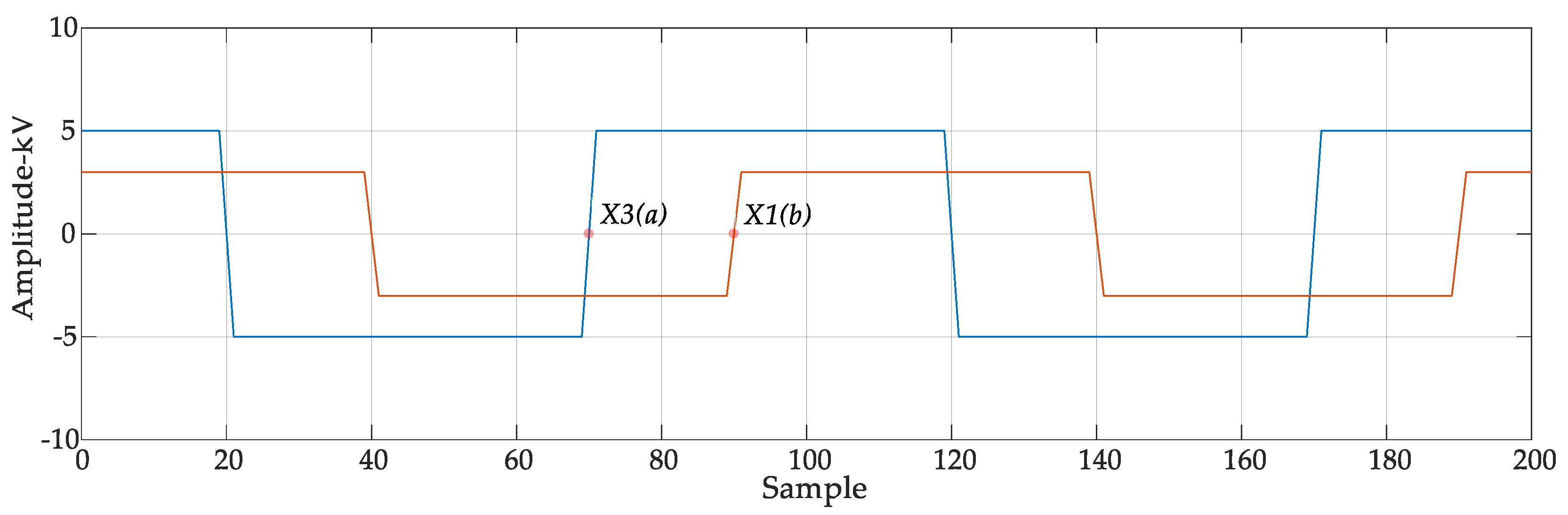
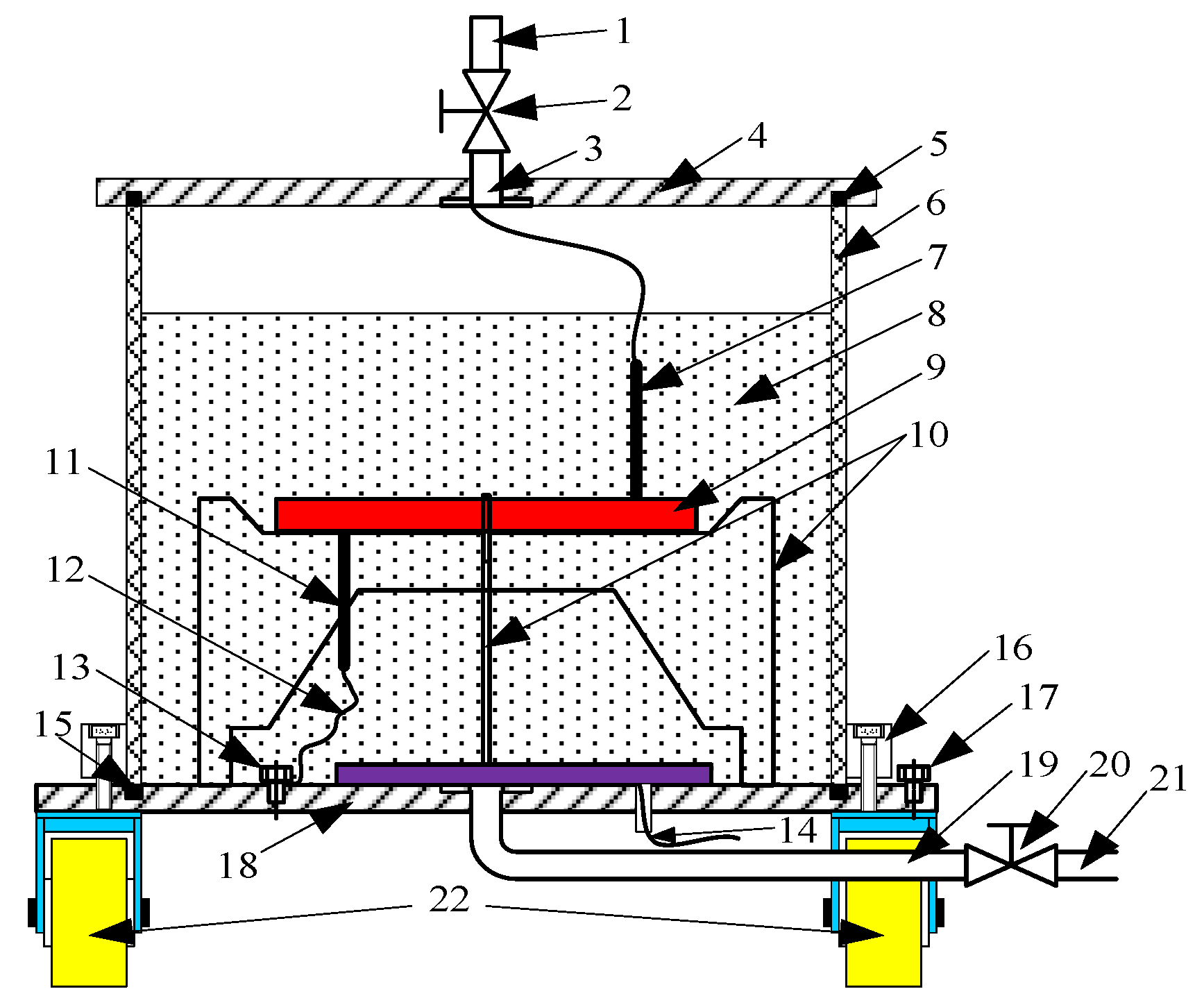
5.1. Experimental Scheme

The frequency of the pulse square voltage is very high; hence, there is little chance of free electrons at the defect in the insulation test sample Cx owing to the short time period. Therefore, the partial discharge initial voltage of the insulation sample under a pulse voltage is higher than that under a power frequency voltage. If the partial discharge initial voltage of the insulation sample is Uc under the power frequency voltage, the partial discharge will not occur under the pulse square voltage when the peak value of the pulse square wave voltage is 0.8 Uc. Therefore, 0.8 Uc can be used as the peak voltage obtained from the first measurement within the secondary measurement method.
In this study, combined with the actual partial discharge measurement, we propose a power interference suppression method of partial discharge under the pulse square voltage based on the secondary measurement. The specific steps are as follows:
(1)
The partial discharge initial voltage Uc of the insulation sample under power frequency voltage was measured.
(2)
The pulse square voltage with a peak value of 0.8 Uc was applied to the insulation sample, where the sampling time was t1 and the measured signal was x1(t).
(3)
The signal x2(t) was measured when there is a partial discharge at the insulation sample. The sampling time was t2 (t1t2 > T, where T is the period of x1(t)).
(4)
The signal x1(t) was processed through the successive interception comparison method, and the corresponding signal X1k(t) was obtained as the benchmark data.
(5)
According to the peak-to-peak ratio of the square voltage of the two measurements, the benchmark signal X1k(t) was transformed linearly and the processed signal and signal x2(t) were then inserted into Equation (6) for power interference suppression.

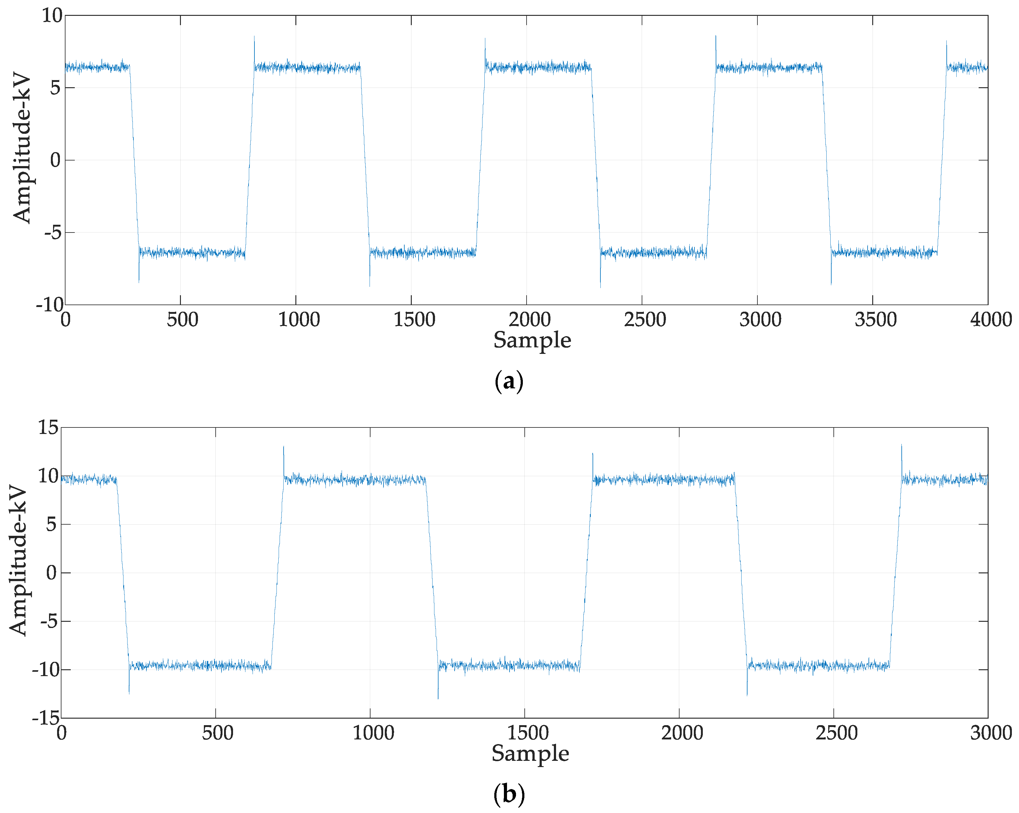
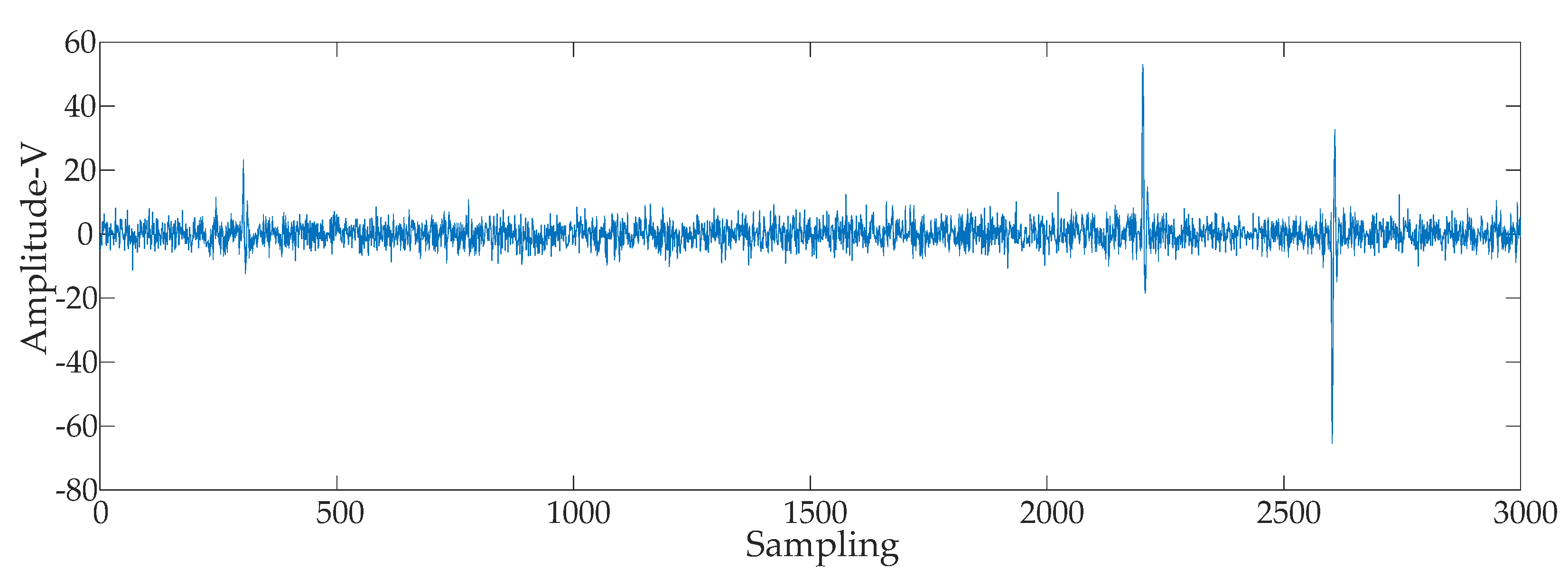
5.2. Experiment and Data Analysis

In this study, a model transformer turn-to-turn oil-paper insulation coil was designed and manufactured as an experimental insulation sample. The model coil adopts a double-cake multiturn ring structure. The specific parameters are as follows: the coil inner diameter was 274 mm; the coil outer diameter was 346 mm; the oil consisted of 2 × 4 = 8 turns; the insulation thickness between turns was 2.45 mm; a flat copper conductor was adopted, with the specification a × b = 2 mm × 10 mm and chamfer radius r = 0.65 mm. The winding method of two strands of paper-wrapped wires was adopted, as shown in Figure 12, in which 1–8 is the same conductor, whereas 1′–8′ is another.
A structural diagram of the model coil is shown in Figure 13, where 1 is the paper-wrapped wire A, 2 is the paper-wrapped wire B, 3 is the white cloth belt, 4 is the cardboard cushion block for support, 5 is the coil outlet end after enhanced insulation, 6 is the terminal of the paper-wrapped wire A and 7 is the terminal of the paper-wrapped wire B. To evenly distribute the electric field, the conductor was connected to the shielding cap and then connected to the circuit.
The oil paper insulation sample must be kept in an oil-immersed state [38,39,40]. The entire test process of a sample needs to be completed in multiple stages, such as placing the sample, vacuuming and pressure aging. The test box must be easy to move, and to eliminate the influence of impurities such as moisture and bubbles to the extent possible, the test chamber must be vacuumed. The designed test oil tank is illustrated in Figure 14. In Figure 14, 1 is the quick connector, 2 is the ball valve, 3 is the stainless steel conduit for air, 4 is the alloy box cover, 5 is the rubber sealing ring, 6 is the epoxy resin pipe, 7 is the high-voltage outlet end of model coil, 8 is the transformer oil, 9 the is model coil, 10 is the insulating support, 11 is the low-voltage outlet end of model coil, 12 is the lead, 13 is the low-voltage lead wiring bolt, 14 is the heating and temperature measuring device and lead, 15 is the rubber sealing ring, 16 is the epoxy resin pipe fixed mounting ring, 17 is the ground wire connecting bolt, 18 is the alloy box bottom, 19 is the stainless steel conduit for transformer oil, 20 is the ball valve, 21 is the quick connector and 22 is the universal casters that can rotate 360 degrees. During the experiment, 1 is connected to the high-voltage terminal and 13 is grounded.
In this study, a partial discharge test platform under high-frequency pulse square voltage was built, and the corresponding test experimental circuit is shown in Figure 15, with a sampling frequency of 20 M samples/s and a sampling time of 200 μs. In Figure 16, the high-frequency pulse square power supply is the PUS-JC-200 high-frequency pulse power supply of Chongqing Pulse Technology, which can output a bipolar high-frequency square pulse voltage signal, with a peak value of 0–40 kV, frequency of 0–20 kHz and voltage rise time of 10 ns–1 μs, with a duty ratio of 50%. R is the protective resistance, CX is the test object, CK is the coupling capacitance and Z is the detection impedance (GSJFY-3000, with a bandwidth of 350 MHz). The data acquisition card is a PicoScope 6000 Series with a bandwidth of 350 MHz, sampling rate up to 5G samples/s, resolution of 1 mV and maximum range of 20 V, the bit resolution is 1:20,000.
According to the method proposed in this study, the power interference in the partial discharge measurement signal is suppressed. The measured signal is shown in Figure 16. The power interference suppression is performed on the data in Figure 16; the waveform after the power interference suppression is shown in Figure 17. It can be seen from Figure 17 that the data contain environmental interference. Using the method proposed in [9], the environmental interference is suppressed, and the waveform is shown in Figure 18. It can be seen that the method proposed in this paper can effectively suppress the power interference under pulsed square wave voltage.
Compared with using the high-pass filter to suppress the power interference, the method proposed in this paper is more economical and does not need to consider the problems of overfiltering and underfiltering. At the same time, the method proposed in this paper avoids the difficulty of adjusting the bridge balance in the balance circuit method. Because it is conducted on two tests on the same sample, it is not necessary to consider that the two samples cannot discharge at the same time. To sum up, the method proposed in this paper has more advantages than the previous methods.

6. Conclusions

In this paper, a power interference suppression method based on quadratic measurement is proposed to suppress the power interference of partial discharge signals under a pulse square voltage. Our research shows that the partial discharge initial voltage under the power frequency voltage is higher than that under the pulse square voltage. According to the partial discharge initial voltage under the power frequency voltage, the peak value of the pulse square voltage during the first measurement within the secondary measurement method can be determined to ensure that no partial discharge occurs in the insulation sample. According to the successive interception comparison method, the first measured data are processed, which can effectively solve the problem that the measurement starting points within the two measurements do not correspond. After the intercepted data are linearly processed, the difference between the second measured data and the intercepted data is calculated to realize the suppression of power interference. The simulation and measured results show that the method proposed in this paper can effectively suppress the power interference in the partial discharge measurement under the pulse square voltage. The proposed method lays the foundation for subsequent studies on the partial discharge characteristics of transformer turn-to-turn oil-paper insulation under pulse square voltage.

Author Contributions

Conceptualization, L.L.; methodology, X.W.; software, L.L.; validation, L.L. and X.W.; formal analysis, L.L. and X.W.; data curation, L.L.; writing—original draft preparation, L.L.; writing—review and editing, L.L.; visualization, L.L.; supervision, X.W.; project administration, X.W. All authors have read and agreed to the published version of the manuscript.

Funding

This research was funded by the National Key Research and Development Program of China, grant number 2017YFB0902705.

Institutional Review Board Statement

Not applicable.

Informed Consent Statement

Not applicable.

Data Availability Statement

Not applicable.

Conflicts of Interest

The authors declare no conflict of interest.

References

  1. Borghei, M.; Ghassemi, M. Partial Discharge Analysis under High-Frequency, Fast-Rise Square Wave Voltages in Silicone Gel: A Modeling Approach. Energies 2019, 12, 4543. [Google Scholar] [CrossRef] [Green Version]
  2. Borghei, M.; Ghassemi, M. A Finite Element Analysis Model for Partial Discharges in Silicone Gel under a High Slew Rate, High-Frequency Square Wave Voltage in Low-Pressure Conditions. Energies 2020, 13, 2152. [Google Scholar] [CrossRef]
  3. Abdelmalik, A.A. Influence of sinusoidal and square voltages on partial discharge inception in geometries with point-like termination. High Volt. 2018, 3, 31–37. [Google Scholar] [CrossRef]
  4. Wang, P.; Yang, N.; Zheng, C.; Li, Y. Effect of repetitive impulsive and square wave voltage frequency on partial discharge features. In Proceedings of the 2018 12th International Conference on the Properties and Applications of Dielectric Materials (ICPADM), Xi’an, China, 20–24 May 2018; pp. 152–155. [Google Scholar] [CrossRef]
  5. Zhao, Y.; Li, Y.; Li, K.; Han, D.; Qiu, Z.; Zhang, G. Emission Spectrum Analysis of Two Typical Partial Discharge Forms under High Frequency Square Wave Voltages. IEEE Access 2020, 8, 219946–219954. [Google Scholar] [CrossRef]
  6. Abdelmalik, A.A.; Nysveen, A.; Lundgaard, L.E. Partial discharges in liquid embedded power electronics: Effects of pressure and liquid nature under negative pulse voltage stress. IEEE Trans. Dielectr. Electr. Insul. 2016, 23, 1119–1125. [Google Scholar] [CrossRef]
  7. You, H.; Wei, Z.; Hu, B.; Zhao, Z.; Na, R.; Wang, J. Partial Discharge Behaviors in Power Modules under Square Pulses with Ultrafast dv/dt. IEEE Trans. Power Electron. 2020, 36, 2611–2620. [Google Scholar] [CrossRef]
  8. Li, L.; Wei, X. Suppression Method of Partial Discharge Interferences Based on Singular Value Decomposition and Improved Empirical Mode Decomposition. Energies 2021, 14, 8579. [Google Scholar] [CrossRef]
  9. Illias, H.A.; Bakar, A.H.A.; Mokhlis, H.; Tunio, M.A.; Chen, G.; Lewin, P.L.; Ariffin, A.M. Simulation of partial discharge within a void under square waveform applied voltage. In Proceedings of the 2012 Annual Report Conference on Electrical Insulation and Dielectric Phenomena, Montreal, QC, Canada, 14–17 October 2012; pp. 76–79. [Google Scholar] [CrossRef] [Green Version]
  10. Qi, W.; Gao, S.; Xia, Y.; Gui, J.; Lin, J.; Huang, J.; Chen, X. Suppression of pulse interference in partial discharge measurement based on phase correlation and waveform characteristics. In Proceedings of the 2014 International Conference on Power System Technology, Chengdu, China, 20–22 October 2014; pp. 1338–1341. [Google Scholar] [CrossRef]
  11. Florkowska, B.; Roehrich, J.; Zydron, P.; Florkowski, M. Measurement and analysis of surface partial discharges at semi-square voltage waveforms. IEEE Trans. Dielectr. Electr. Insul. 2011, 18, 990–996. [Google Scholar] [CrossRef]
  12. Nguyen, H.V.P.; Phung, B.T.; Blackburn, T. Partial discharge behaviors in cavities under square voltage excitation at very low frequency. In Proceedings of the 2016 International Conference on Condition Monitoring and Diagnosis (CMD), Xi’an, China, 20–25 September 2016; pp. 866–869. [Google Scholar] [CrossRef]
  13. Wang, P.; Xu, H.; Wang, J.; Cavallini, A. The influence of repetitive square wave voltage duty cycle on partial discharge statistics and insulation endurance. In Proceedings of the 2016 International Conference on Condition Monitoring and Diagnosis (CMD), Xi’an, China, 20–25 September 2016; pp. 274–277. [Google Scholar] [CrossRef]
  14. Chen, X.; Cao, B.; Wu, G.; Gao, G.; Sun, J.; Gu, Z. Use of UHF method to measure partial discharge signal under square quare-wave pulse. In Proceedings of the 2014 International Symposium on Electrical Insulating Materials, Niigata, Japan, 1–5 June 2014; pp. 188–191. [Google Scholar] [CrossRef]
  15. Jiang, J.; Zhang, B.; Li, Z.; Ranjan, P.; Chen, J.; Zhang, C. Partial Discharge Features for Power Electronic Transformers under High-Frequency Pulse Voltage. IEEE Trans. Plasma Sci. 2021, 49, 845–853. [Google Scholar] [CrossRef]
  16. Hu, B.; Wei, Z.; You, H.; Na, R.; Liu, R.; Xiong, H.; Fu, P.; Zhang, J.G.; Wang, J. A Partial Discharge Study of Medium-Voltage Motor Winding Insulation under Two-Level Voltage Pulses with High Dv/Dt. IEEE Open J. Power Electron. 2021, 2, 225–235. [Google Scholar] [CrossRef]
  17. Wang, P.; Cavallini, A.; Montanari, G.C. Characteristics of PD under square wave voltages and their influence on motor insulation endurance. EEE Trans. Dielectr. Electr. Insul. 2015, 22, 3079–3086. [Google Scholar] [CrossRef]
  18. Wang, P.; Cavallini, A.; Montanari, G.C.; Wu, G. Effect of rise time on PD pulse features under repetitive square wave voltages. IEEE Trans. Dielectr. Electr. Insul. 2013, 20, 245–254. [Google Scholar] [CrossRef]
  19. Wu, K.; Okamoto, T.; Suzuoki, Y. Effects of discharge area and surface conductivity on partial discharge behavior in voids under square voltages. IEEE Trans. Dielectr. Electr. Insul. 2007, 14, 461–470. [Google Scholar] [CrossRef]
  20. Baug, A.; Choudhury, N.R.; Ghosh, R.; Dalai, S.; Chatterjee, B. Identification of single and multiple partial discharge sources by optical method using mathematical morphology aided sparse representation classifier. IEEE Trans. Dielectr. Electr. Insul. 2017, 24, 3703–3712. [Google Scholar] [CrossRef]
  21. Santos, M.G.; Braulio, G.A.; Bernardes, J.V.; De Salles, C.; Milanez, J.R.C.; Bortoni, E.C.; Bastos, G.S. Continuous Partial Discharges Analysis during Automated Thermal Cycle Aging Experiment. IEEE Trans. Energy Convers. 2020, 35, 1989–1992. [Google Scholar] [CrossRef]
  22. Wu, Y.; Wang, G.; Bi, J.; Li, J.; Peng, X.; Liu, T. Interference Rejection of High Voltage Cables Partial Discharge Detection Based on Combination Features Analysis. In Proceedings of the 2019 IEEE PES Asia-Pacific Power and Energy Engineering Conference (APPEEC), Macao, China, 1–4 December 2019; pp. 1–5. [Google Scholar]
  23. Rajendran, A.; Meena, K.P.; Buijupati, N.R. Simulation of partial discharges and implementation of noise elimination techniques. In Proceedings of the 2017 3rd International Conference on Condition Assessment Techniques in Electrical Systems (CATCON), Rupnagar, India, 16–18 November 2017; pp. 412–417. [Google Scholar]
  24. Shams, M.A.; Anis, H.I.; El-Shahat, M. Denoising of Heavily Contaminated Partial Discharge Signals in High-Voltage Cables Using Maximal Overlap Discrete Wavelet Transform. Energies 2021, 14, 6540. [Google Scholar] [CrossRef]
  25. Soltani, A.A.; El-Hag, A. Denoising of Radio Frequency Partial Discharge Signals Using Artificial Neural Network. Energies 2019, 12, 3485. [Google Scholar] [CrossRef] [Green Version]
  26. Zhu, J.; He, B.; Wang, X.; Cui, L.; Li, Y. Extraction of Partial Discharge Signal Feature Based on Dual-tree Complex Wave-let Transform and Singular-value Decomposition. In Proceedings of the 2018 Condition Monitoring and Diagnosis (CMD), Perth, WA, Australia, 23–26 September 2018; pp. 1–5. [Google Scholar]
  27. Ran, H.; Xu, Y.; Jiang, J.; Tang, K.; He, Z.; Zhang, T.; Tang, X. Application of Singular Value Reconstruction in Suppressing Narrowband Interference of Partial Discharge. In Proceedings of the 2019 4th International Conference on Power and Renewable Energy (ICPRE), Chengdu, China, 21–23 September 2019; pp. 239–243. [Google Scholar]
  28. Zhou, K.; Li, M.; Li, Y.; Xie, M.; Huang, Y. An Improved Denoising Method for Partial Discharge Signals Contaminated by White Noise Based on Adaptive Short-Time Singular Value Decomposition. Energies 2019, 12, 3465. [Google Scholar] [CrossRef] [Green Version]
  29. Wei, L.; Liu, Y.; Cheng, D.; Li, P.; Shi, Z.; Huang, N.; Ai, H.; Zhu, T. A Novel Partial Discharge Ultra-High Frequency Signal De-Noising Method Based on a Single-Channel Blind Source Separation Algorithm. Energies 2018, 11, 509. [Google Scholar] [CrossRef] [Green Version]
  30. Zhong, J.; Bi, X.; Shu, Q.; Chen, M.; Zhou, D.; Zhang, D. Partial Discharge Signal Denoising Based on Singular Value Decomposition and Empirical Wavelet Transform. IEEE Trans. Instrum. Meas. 2020, 69, 8866–8873. [Google Scholar] [CrossRef]
  31. Govindarajan, S.; Subbaiah, J.; Cavallini, A.; Krithivasan, K.; Jayakumar, J. Partial Discharge Random Noise Removal Using Hankel Matrix-Based Fast Singular Value Decomposition. IEEE Trans. Instrum. Meas. 2019, 69, 4093–4102. [Google Scholar] [CrossRef]
  32. Yang, X.; Huang, H.; Shu, Q.; Zhang, D.; Chen, B. Partial Discharge Signal Extraction Method Based on EDSSV and Low Rank RBF Neural Network. IEEE Access 2021, 9, 9744–9752. [Google Scholar] [CrossRef]
  33. Barbi, I. A Theorem on Power Superposition in Resistive Networks. IEEE Trans. Circuits Syst. II Express Briefs 2021, 68, 2362–2363. [Google Scholar] [CrossRef]
  34. Leni, P.E.; Fougerolle, Y.D.; Truchetet, F. Kolmogorov Superposition Theorem and Wavelets for image compression. IET Image Process. 2010, 6, 753502. [Google Scholar]
  35. Zhang, Z.; Shen, A.; Li, P.; Luo, X.; Tang, Q. MTPA-based high-frequency square wave voltage signal injection strategy for IPMSM control. J. Power Electron. 2021, 21, 1461–1472. [Google Scholar] [CrossRef]
  36. Karakaya, F.; Gülsuna, Ö.; Keysan, O. Feasibility of Quasi-Square-Wave Zero-Voltage-Switching Bi-Directional DC/DC Converters with GaN HEMTs. Energies 2021, 14, 2867. [Google Scholar] [CrossRef]
  37. Shen, L.; Xie, F.; Xiao, W.; Ji, H.; Zhang, B. Thermal Analyses of Reactor under High-Power and High-Frequency Square Wave Voltage Based on Improved Thermal Network Model. Electronics 2021, 10, 1342. [Google Scholar] [CrossRef]
  38. Zhang, T.; Mandala, A.T.; Zhong, T.; Jiang, S.; Zhang, N. The Dielectric Voltage Response Characteristics of Transformer Oil–Paper Insulation and Its Aging State Assessment. MAPAN 2022. [Google Scholar] [CrossRef]
  39. Luo, B.; Wang, J.; Dai, D.; Jia, L.; Li, L.; Wang, T. Partial Discharge Simulation of Air Gap Defects in Oil-Paper Insulation Paperboard of Converter Transformer under Different Ratios of AC–DC Combined Voltage. Energies 2021, 14, 6995. [Google Scholar] [CrossRef]
  40. Zukowski, P.; Rogalski, P.; Kierczynski, K.; Koltunowicz, T.N. Precise Measurements of the Temperature Influence on the Complex Permittivity of Power Transformers Moistened Paper-Oil Insulation. Energies 2021, 14, 5802. [Google Scholar] [CrossRef]
Figure 1. PD simulation signals. (a) PD simulation signals x1(t) when fc = 2 MHz and τ = 0.3 μs. (b) PD simulation signals x2(t) when fc = 0.2 MHz and τ = 3 μs.
Energies 15 03437 g001
Figure 2. Impulse square voltage applied to the insulation sample.
Energies 15 03437 g002
Figure 3. Equivalent circuit with no partial discharge in Cx.
Energies 15 03437 g003
Figure 4. Equivalent circuit with partial discharge in Cx.
Energies 15 03437 g004
Figure 5. Equivalent circuit using the superposition principle.
Energies 15 03437 g005
Figure 6. Pulse square voltages with the same parameters but different peak values.
Energies 15 03437 g006
Figure 7. Simulation waveform of pulse square voltage.
Energies 15 03437 g007
Figure 8. Simulation waveform of the pulse square voltage superimposed partial discharge signal. (a) Pulse square voltage superimposed partial discharge (PD) simulation signals x1(t) when fc = 2 MHz and τ = 0.3 μs and pulse square voltage s(t). (b) Pulse square voltage superimposed partial discharge (PD) simulation signals x2(t) when fc = 0.2 MHz and τ = 3 μs, and pulse square voltage s(t).
Energies 15 03437 g008aEnergies 15 03437 g008b
Figure 9. Simulation signal after removing power interference. (a) PD simulation signal with fc = 2 MHz and τ = 0.3 μs after removing power interference. (b) PD simulation signal with fc = 0.2 MHz and τ = 3 μs after removing power interference.
Energies 15 03437 g009
Figure 10. Measurement of time difference.
Energies 15 03437 g010
Figure 11. Schematic diagram of intercept data.
Energies 15 03437 g011
Figure 12. Method of coil winding.
Energies 15 03437 g012
Figure 13. Structural diagram of the model coil.
Energies 15 03437 g013
Figure 14. Schematic diagram of the oil tank used for the test.
Energies 15 03437 g014
Figure 15. Experimental circuit diagram.
Energies 15 03437 g015
Figure 16. Data from two experiments. (a) First measured data. (b) Second measured data.
Energies 15 03437 g016
Figure 17. Measurement signals with power interference suppressed.
Energies 15 03437 g017
Figure 18. Measurement signals with environment interference suppressed.
Energies 15 03437 g018
Table 1. PD simulation signal parameters.
Partial Discharge (PD) PulseA1B1C1D1
Signal amplitude (A/V)10101010
Oscillation frequency (fc/MHz)-2-2
Attenuation coefficient (τ/μs)0.30.30.30.3
Time of PD (t0/μs)050100150
Partial Discharge (PD) PulseA2B2C2D2
Signal amplitude (A/V)10102020
Oscillation frequency (fc/MHz)-0.2-0.2
Attenuation coefficient (τ/μs)3333
Time of PD (t0/μs)050100150
Publisher’s Note: MDPI stays neutral with regard to jurisdictional claims in published maps and institutional affiliations.

