Abstract
The main purpose of this study was to develop a photovoltaic module array (PVMA) and an energy storage system (ESS) with charging and discharging control for batteries to apply in grid power supply regulation of high proportions of renewable energy. To control the flow of energy at the DC load and charge/discharge the battery uniformly, this work adapted a bidirectional buck–boost soft-switching converter and the maximum power point tracking (MPPT) technique of the photovoltaic module array. First, a boost converter is used with the perturb and observe (P&O) method, so that the photovoltaic module array can work at the maximum power point (MPP) at any time. When the output power of the photovoltaic module array is greater than the load power, the excess power is used to charge the battery; on the contrary, if the output power of the photovoltaic module array is lower than the load power, the battery discharges for auxiliary power supply. This makes the voltage of the DC link maintain a constant value. The monitoring circuit sends the voltage and current signals to the TMS320F2809 digital signal processor (DSP) produced by Texas Instruments to control the battery charging/discharging voltage and current. The photovoltaic module array works at the MPP to improve the performance of the overall energy storage system. Finally, the actual test result shows that the soft-switching converter used in this work, when compared to the hard-switching converter, can improve efficiency by nearly 4% when the load power is above 125 W. When the photovoltaic power generation system operation is between 150 W and 400 W, the proposed uniform charging and discharging architecture can rapidly reach uniformity.
1. Introduction
A microgrid is a small electrical grid that is developed in combination with renewable energy. Photovoltaic and wind power generation are the most common power supplies for microgrids, which means that these electrical grid systems can be independently operated. However, the power generation quantity of renewable energy generation systems varies according to the weather, which can affect the power generation efficacy [1,2,3]. For example, photovoltaic power generation will change based on sunlight exposure, creating unstable power generation (unstable power supply between the load and the power grid). Thus, a battery energy storage system must be used to conduct power adjustment in photovoltaic power generation. This allows the photovoltaic power generation system to store excess power in the batteries and use the batteries to supply power when the microgrid does not have enough power to supply, allowing the microgrid to achieve maximum benefit.
With the rapid growth in global photovoltaic power generation, there will be a large number of photovoltaic power generation systems (PVPGS) parallel connected to the power grid system. However, when the proportion of renewable energy power generation becomes higher, the voltage and frequency change rate of the power system may be greater, limiting the grid-connected capacity of photovoltaics and also causing the power quality of the regional power grid to decline. As the photovoltaic power generation system reduces its power generation during the nighttime or when the weather is poor, if the power company’s backup capacity is insufficient, it will lead to regional power outages or even complete power outages, gradually creating the problem of connecting photovoltaic and city power grids. Therefore, the development of an energy storage system for photovoltaic power generation systems, which allows photovoltaic power generation systems to adjust the power supply to the load side of the grid through the energy storage of the battery when the power generation is excessive or plummeting, is an urgent research topic.
Generally, when batteries leave the factory, the condition of each battery will be different, such as internal impedance and the self-discharge rate. If different manufacturers produce them, their internal chemical structures and battery-rated voltages will also be different. In addition, if the battery is close to the heat source, the charge and discharge reaction of the battery will be different. Therefore, when batteries are used in serial connection, if there is no protection mechanism, or it does not employ a uniform charge and discharge structure, the battery will be overcharged or over-discharged. Overcharge or over-discharge will accelerate battery aging and cause the battery’s capacity and life span to be reduced, or even worse, the battery will explode. Therefore, when charging and discharging serially connected batteries, a structure of uniform charging and discharging must be added to achieve the effect of protecting the batteries. Currently, common uniform charging and discharging methods are divided into passive and active. The passive is resistive [4,5,6,7], and the active includes capacitive, inductive, and multiple winding transformer types and equal charge bidirectional buck–boost hard-switching converters [8,9,10,11,12,13,14,15,16,17,18,19,20,21], and so on. For fixed-resistor uniform charge and discharge architecture [4,5], each battery is parallel connected with a resistor, which consumes the energy of the highest battery voltage first, until the highest battery voltage value is equal to the lowest battery voltage value. Although this architecture is simple and low-cost, the continuous parallel resistor makes the entire system consume a lot of extra energy. In addition, it generates heat on the resistor, which reduces efficiency. Although the switching-resistor type uniform charge and discharge circuit architecture [6,7] consumes less energy than the fixed type, it requires a higher power consumption resistor and a higher current endurance switch than the active uniform charge and discharge switches, and the power consumption on the resistor is relatively high. The capacitor type uniform charge and discharge architecture [8,9,10,11] is one of the active uniform charge and discharge architectures. It is a structure composed of a serially connected battery through a bidirectional switch and a capacitor. This architecture uses capacitors to store energy. This feature solves the problem of uniform charging and discharging of the battery. The advantage of this architecture is that the loss is low, but when the energy is too much, the problem of having nowhere to go will occur, and the uniform charge and discharge time is also very long. Moreover, if you want to shorten the charge and discharge time, you need to use a larger capacitor to make the overall circuit bulky and increase the cost. Thus, it is not easy to implement in a large-capacity energy storage system. The inductive type uniform charge/discharge architecture can be further divided into forward [12,13] and backward [14,15]. The energy conversion of this type of architecture is limited by the capacity of the inductor. When the inductor with a higher battery voltage is charged, the battery’s power will be reduced. Charging speed causes the problem of an overly long charging time. The multi-winding transformer’s uniform charging and discharging architecture [16,17,18,19] stores energy on the primary side of the transformer first, then transfers the excess energy to the low-voltage battery through the secondary side. Although the balance speed can be greatly shortened, it is relatively derived from the problem of a relatively expensive transformer design cost, and there will be problems of hysteresis loss, mutual inductance, and leakage inductance. Thus, it is difficult to design a circuit for this architecture compared to other circuit architectures. With bidirectional buck–boost hard-switching converter uniform charge/discharge architecture [20,21] operating in boost mode, the battery pack is the input terminal and provides energy to the load at the output terminal. When operating in the buck mode, the voltage of the DC power supply terminal is greater than the voltage of the battery pack, and the battery pack is in the charging state. This architecture is only suitable for a single battery with a larger capacity. If it is used in a battery with a small capacity, it will increase the cost, and the switch in the circuit adopts hard switching, it is easy to cause the power loss of the switch during the switching process. The passive uniform charging and discharging architecture proposed in [4,5,6,7] has the advantage of having a simple circuit and low cost. However, these architectures have low efficiency, and the battery uniform charging and discharging time takes longer than the active uniform charging and discharging architecture. The active uniform charging and discharging architecture proposed in reference [8,9,10,11,12,13,14,15,16,17,18,19,20,21] has a short uniform charging and discharging time, but the architecture and control are complex. The uniform charging and discharging architecture developed for this work has a soft-switching function that can reduce the switching loss caused by the switching of power semiconductors, thereby improving converter efficiency. At the same time, the uniform charging and discharging control strategy proposed for this work can simplify the uniform charging and discharging procedure and shorten the uniform charging and discharging.
In addition, because the photovoltaic module is a non-linear component, the voltage, current, and output power of the photovoltaic module will vary due to factors such as the amount of sunlight and ambient temperature, so its P–V and I–V characteristic curves will also change accordingly. Suppose the load is directly connected to the photovoltaic module array. In this case, the photovoltaic module array will not operate at the maximum power point, resulting in the inability to provide the maximum power to the load. Therefore, in order to maintain the output power of the photovoltaic power generation system at the maximum power point, it must be equipped with a maximum power tracker [22,23].
Based on this, this work proposes the bidirectional buck–boost soft-switching converter, as shown in Figure 1, as the control architecture of the energy storage system [24,25]. The architecture controls the charging and discharging of the battery. Moreover, this bidirectional buck–boost converter architecture replaces the diodes of the boost converter architecture with switching components, making the architecture have buck, boost, and energy bidirectional flow characteristics. In addition, if the low-voltage side is combined with a battery, and the high-voltage side is connected to the photovoltaic power generation system, it has the function of storing excess power and auxiliary power supply. At the same time, it can be used with the most commonly used perturb and observe (P&O) method [22] to track the maximum power of the photovoltaic module array. In the actual test part, the TMS320F2809 digital signal processor [26] is used for switching control to control the charging and discharging of the battery. The performance of the energy storage system developed under loads of 100 W and 300 W was verified.
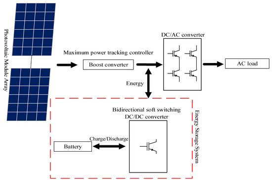
Figure 1.
The system architecture of the photovoltaic module array and uniform charge/discharge control energy storage battery system.
The arrangement of the various section contents is as follows: Section 2 describes the advantage of the P&O method and its tracking process compared to the current traditional maximum power point tracking (MPPT). Section 3 describes the pulse width modulation (PWM) control signal used by the bidirectional buck–boost soft-switching converter’s circuit architecture and various power semiconductor switches. Section 4 describes the architecture and circuit design of the uniform charging and discharging converter and introduces their control rules. Section 5 compares the efficiency test results of the soft-switching mode converter compared to that of the traditional hard-switching mode converters, and uses a uniform charging and discharging response to verify the feasibility of combining the uniform charging and discharging control architecture with photovoltaic power generation systems. Finally, the conclusion of this article describes the results of this work and what limitations may be encountered in the application of this architecture. The conclusion also proposes some recommendations for future research.
2. The Adopted Maximum Power Point Tracking (MPPT) Control Methodology
Due to its simple circuit and fewer parameters, the perturb and observe (P&O) method does not need to measure the parameters of the photovoltaic module array. It is most commonly used in many algorithms. It continuously adds disturbance to the terminal voltage of the photovoltaic module array in a fixed period. If the terminal voltage increases the output power of the photovoltaic module array due to the disturbance, the disturbance in the same direction will be used next time to change the voltage of the photovoltaic module array, continuing to disturb, observe, and compare until it reaches the maximum power point. The process flow of the disturbance is shown in Figure 2 [22,23].
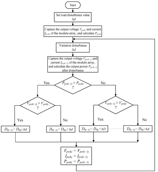
Figure 2.
The flow chart of P&O method.
3. Bidirectional Buck–Boost Soft-Switching Converter
The switching loss caused by the switching of the converter will not only make the switching element heat up but also reduce the efficiency of the converter. In addition, it will cause high dv/dt and di/dt, and even cause serious electromagnetic interference (EMI). Based on this, this study adopted a bidirectional buck–boost soft-switching converter [24,25]. The converter architecture and switching signal output are shown in Figure 3a,b. This converter is based on the existing bidirectional converter hard-switching architecture, supplemented by a set of resonant branches. This resonance branch is composed of a high-voltage side auxiliary switch SHr, low-voltage side auxiliary switch SLr, resonance inductance Lr, and resonant capacitor CLr, which are controlled by the pulse width modulation (PWM) signal to turn on the auxiliary switch. After the resonant branch forms transient resonance, the main switching component is switched so that this converter has zero voltage switching (ZVS) and zero current switching (ZCS) soft-switching characteristics.
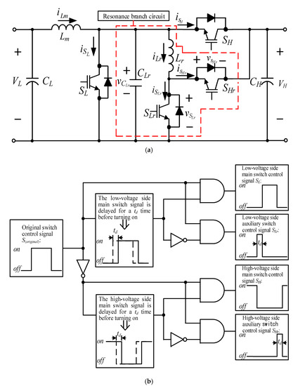
Figure 3.
The bidirectional buck–boost soft-switching converter: (a) circuit architecture; (b) schematic diagram of switch signal output control.
4. An Energy Storage System with Uniform Charge/Discharge Control
The internal resistance and self-discharge rate of each battery cause differences in its health status. Thus, when batteries are parallel connected, and no protective mechanism or uniform charging and discharging architecture is used, battery overcharge or over-discharge can result. This work uses a bidirectional buck–boost soft-switching converter and proposes a new uniform charging and discharging architecture so that battery power can quickly achieve uniformity. This converter has ZVS and ZCS functions, which allow it to effectively improve the efficiency of uniform charging and discharging circuits.
4.1. Battery Energy Storage System Architecture with Uniform Charge and Discharge Control
A retired battery’s capacity is 70~80% of that of a brand new battery, and each battery has a different health status, which will cause uneven charging and discharging of the battery. Using the uniform charging and discharging architectures in the literature [4,5,6,7,8,9,10,11,12,13,14,15,16,17,18,19,20,21], they can prevent the battery from overcharging and over-discharging, and adjust the charging and discharging current for each battery to make the battery charge and discharge uniformly. However, these methods all have problems such as low efficiency, high cost, slow charging speed, and complex circuits. Therefore, this work proposes a bidirectional buck–boost soft-switching converter, as shown in Figure 4, for a single charge/discharge uniform charge and discharge architecture. This architecture contains a sensing circuit, a switching component for the isolated drive circuit, a digital signal processor, and a dual-set serial connected bidirectional buck–boost soft-switching converter. The sensing circuit includes voltage detection and current detection. The switching component for the isolation drive circuit is mainly used to enable the TMS320F2809 digital signal processor [26] to generate a pulse width modulation (PWM) signal to control the on and off of the power switch and achieve the electrical isolation between the control circuit and the power circuit. In addition, the dual-set serial connected bidirectional buck–boost soft-switching converter [24,25] not only has both boost and buck functions but also has the characteristics of soft switching, so it can significantly improve the efficiency of electrical energy conversion. When this architecture is operated in the boost mode, the battery pack is the input end and provides energy to the high-voltage output end. If it is operated in the buck mode, the voltage of the DC power end is greater than the voltage of the battery pack, and the battery pack is in a charging state.
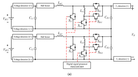
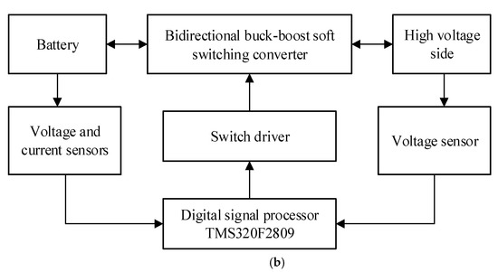
Figure 4.
An energy storage system with uniform charge/discharge control: (a) circuit architecture; (b) block diagram.
This work uses a dual-set serial-connected bidirectional buck–boost soft-switching converter, as shown in Figure 4a, so there are two battery parameters on the battery side. The parameters and electrical specifications are shown in Table 1.

Table 1.
The electricity specification of the bidirectional buck–boost soft-switching converter.
4.1.1. Main Inductance Lm1, Lm2 Design
The converter is designed so that the inductor current is in the discontinuous current mode (DCM) when the load is light. When the load is loaded, the current is operated in the continuous conduction mode (CCM); this design can reduce the switch conduction loss of the load when the load is light. The inductance values of the buck mode and the boost mode can be obtained by Equations (1) and (2), respectively [24,25]. However, in order to ensure that the current can be operated in CCM in both the buck and the boost modes when the boost mode value is selected and the duty cycle D = 0.33, the required inductance value is the largest, the high voltage side voltage is VH = 240 V, and the light load critical power is PH = 150 W. Thus, from Equation (1), we can derive that the required minimum inductance value is 1.14 mH. In addition, in order to ensure that the designed converter can operate in continuous conduction mode, the inductance must be multiplied by 1.25 times, so Lm1 and Lm2 need to use 1.425 mH.
4.1.2. Capacitor CL1, CL2, CH1, CH2 Design
While the switch is turned on and off, it will produce output ripple voltage in order to make the output more stable, so the input and output are connected in parallel with a filter capacitor to filter out ripple voltage. The low voltage end capacities CL1 and CL2 could be derived from Equation (3), CL1 = CL2 = 189 μF [24,25], and the high voltage end capacities CH1 and CH2 could be derived from Equation (4), CH1 = CH2 = 42 μF [24,25]. Therefore, this study adopted a capacity value of CL1 = CL2 = CH1 = CH2 = 270 μF/450 V, which is easier to acquire.
4.1.3. The Design of the Main Power Switch Component and the Auxiliary Power Switch Component
The maximum current routes through the main power switching components SL1, SL2, SH1, and SH2 could be derived from Equation (5) [24,25]. From the Table 1 specifications, we know that the maximum voltage that the main switch components SL1, SL2, SH1, and SH2 should be able to endure is 240 V. In addition, considering the need to compare the circuit efficiency of the hard-switching and soft-switching architectures in the actual test, in order to avoid the surge voltage and surge current caused by the hard-switching architecture at the switching moment, which might cause the switching components to burn out, IGBT -IXGH40N120C3D1 (40 A/1200 V) is used as the main switching component. In addition, the maximum voltage on the auxiliary switches SLr1, SLr2, SHr1, and SHr2 is the same as the maximum voltage on the main switch component, and the current flowing through the auxiliary switch is close to the main switch current, so the auxiliary switch selected was the same as the main switch component.
4.1.4. Resonant Component Design
Based on the circuit analysis, resonance inductance Lr1, Lr2 and resonance capacitor Cr1, Cr2 could be determined by Equation (6) [24,25]. In order to ensure that Equation (6) met the requirements regardless of a light or heavy load, the maximum value of the inductor current ILm, that is, the peak value of iLm at full load , was used to determine the on-time tD of the auxiliary switch, and tD is usually 5~10% of the switching period T. A margin time is required to obtain a reliable tD, so here, we set = 0.1 T = 4 μs, and = 0.01 T = 0.4 μs, and then used Equation (6) to derive the maximum resonance inductance value Lr1 = Lr2 = 38 μH so that we could select a resonance inductance value smaller than 38 μH that would work. In addition, the selected switching component IGBT-IXGH40N120C3D1 has a stray capacitance of 202 pF, so the resonance capacitors Cr1 and Cr2 can be replaced by stray capacitors.
4.2. The Control Mode of Uniform Charging/Discharging
Because each battery has a different SOC, when batteries are parallel connected for charging and discharging, a power imbalance problem can result. Consequently, batteries can overcharge and over-discharge. References [27,28,29,30] show that if batteries are improperly charged and discharged, this can prematurely age or damage the batteries. However, the uniform charging and discharging architecture proposed in this work independently charges and discharges each battery so that they can rapidly achieve uniform charging and discharging. This architecture also effectively limits the charging and discharging current to reduce battery aging problems. Because this work used KUNG LONG WP12-12 12 V/12 Ah lead-acid batteries, the upper limit for the charging and discharging current command was set at a 0.3 C rate to extend the battery life, which resulted in a longer battery charging time. If this is changed to lithium-ion batteries, then the charging and discharging current upper limit must be changed. Figure 5 is a control block diagram for uniform charge and discharge. First, the voltage of the battery pack must be sent back from the voltage sensor to the digital signal processor (DSP). Then the average voltage of the battery pack Vavg is calculated by Equation (7), and the voltage of the Nth battery pack VBTN is compared with the average voltage Vavg. The error of the subtraction from the average voltage is evN. If evN is a positive value, this means that the battery can continue to discharge; on the contrary, if it is a negative value, this means that the battery should be charged. The error value evN goes through a proportional integral (PI) controller, and the battery charge and discharge current command can be obtained; the calculation is shown in Equation (8). When the evN difference is greater, the charge and discharge current command value is greater; on the contrary, if the evN difference is smaller, the charge and discharge current command value is smaller. During the charging and discharging of the battery, the maximum charge current and discharge current limit must be set. If the limit is exceeded, the battery is easily damaged. Therefore must be controlled within the maximum charge and discharge current by the DSP. Then, by comparing the current error generated by the PI controller, the control signal Icontrol is obtained, and the control signal Icontrol is then compared with the triangle wave to obtain the PWM signal. If Icontrol is larger, the on time of switch SLN is longer, that is, the duty cycle is larger; on the contrary, if Icontrol is smaller, the on time of SLN is shorter, that is, the duty cycle is shorter, so that the charge and discharge current of each battery pack can be adjusted to achieve the goal of uniform charge and discharge of the battery pack. The comparison of the relationship between and evN is shown in Table 2, and Table 3 shows the comparison between Icontrol and the on/off time of the uniform charge/discharge control.
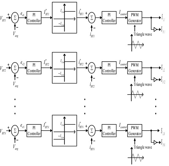
Figure 5.
The control block diagram of the uniform battery pack charging/discharging.
Table 2.
The mapping table of uniform charging.
Table 3.
Uniform charge and discharge control switch on time comparison table (N ≥ 1).
5. Test Results
This work used a Kernel PVS01202 photovoltaic power simulator as the photovoltaic power array output. The batteries used were KUNG LONG WP12-12 12 V/12 Ah lead-acid batteries. The TMS320F2809 digital signal processor [26] was used as the control core of the architecture in Figure 4. TMS320F2809 is a fast and powerful digital signal microprocessor with low power consumption. It has a RAM of 36 KB and a Flash memory of 128 KB, and its working clock pulse can reach a maximum of 100 MHz. The uniform charging and discharging circuit architecture proposed for this work was composed of multiple bidirectional buck–boost soft-switching converters. Thus, more PWM control modules and analog–digital converter (ADC) channels were required. The TMS320F2809 has 12 PWM control modules and 16 sets of 12 bit ADC channels. Therefore, this work employed this digital signal processor to control the batteries’ uniform charging and discharging. Voltage and current sensor signals were transmitted to the DSP for calculation. The proposed uniform charging and discharging control program was developed using C language and TI Code Composer Studio (CCS) development environment. Converter switch waveforms and a uniform charging and discharging response diagram from this section’s actual test were used to verify the performance of the energy storage system composed of the proposed photovoltaic power generation system and the uniform charging and discharging batteries.
5.1. The Actual Test for the Bidirectional Buck–Boost Soft-Switching Converter
The physical circuit of the proposed architecture is shown in Figure 6. Figure 7 and Figure 8 show the actual test waveform of each switch component for the bidirectional buck–boost soft-switching converter operating in buck mode and boost mode at a load of 300 W, respectively.
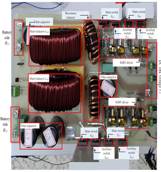
Figure 6.
Dual sets serial connected bidirectional buck–boost soft-switching converter physical circuit diagram.
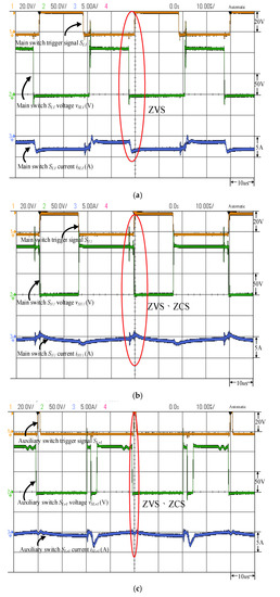
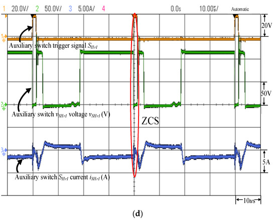
Figure 7.
The actual test waveform for buck mode; the load is 300 W for each switch component: (a) main switch SL1; (b) main switch SH1; (c) auxiliary switch SLr1; (d) auxiliary switch SHr1.
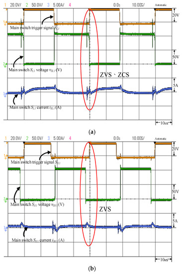
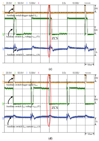
Figure 8.
The actual test waveform for boost mode; the load is 300 W for each switch component: (a) main switch SL1; (b) main switch SH1; (c) auxiliary switch SLr1; (d) auxiliary switch SHr1.
The actual test results of the load from 50 W to 300 W prove that the adopted converter can achieve the purpose of soft switching the main switch under various loads, regardless of whether it is operated in the buck mode or the boost mode. Therefore, the switching loss generated at the moment of the main switch switching can be reduced, and the conversion efficiency of the converter can be improved. Figure 9a,b is the actual efficiency comparisons of the adopted soft-switching converter and the traditional hard-switching converter when operating in the buck and boost modes. The figure shows that the efficiency of the soft-switching converter used in the buck mode or boost mode is nearly 4% higher than that of the hard-switching converter when the load power is more than 125 W.
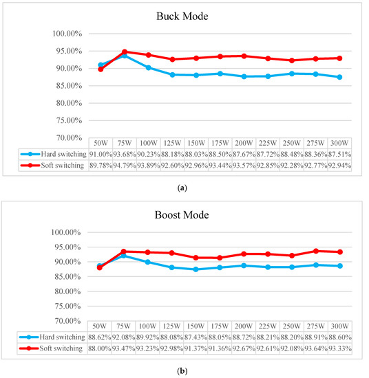
Figure 9.
The actual test efficiency comparison between traditional hard-switching and proposed soft-switching converter: (a) buck mode; (b) boost mode.
The existing automatic uniform charging and discharging circuit architecture mostly utilizes a hard-switching mode converter, leading to high switching loss and poor overall system efficiency. To improve this problem, this work proposes a type of soft-switching-mode uniform charging and discharging circuit architecture to lower switching loss and improve battery charging and discharging efficiency. Furthermore, this work also proposes a simple uniform charging and discharging control strategy to independently control the charging and discharging of each battery. This allows each battery to rapidly achieve uniform charging and discharging. The test results in Figure 9 prove that compared to traditional uniform charging and discharging circuit architecture, the proposed architecture can effectively improve charging and discharging efficiency by over 4%. Therefore, the uniform charging and discharging circuit architecture proposed in this work is innovative.
5.2. The Actual Test on Associating Uniform Charging/Discharging Battery with Photovoltaic Power Generation System
Figure 10 shows the hardware circuit architecture of the developed battery energy storage system with uniform charge and discharge. The actual test of battery uniform charge and discharge control used two sets of different battery voltages combined with photovoltaic modules and maximum power tracking technology to conduct a uniform charge and discharge control experiment. Table 4 shows the initial voltage of each set of batteries and the final voltage after uniform charging and discharging under different photovoltaic module output powers.
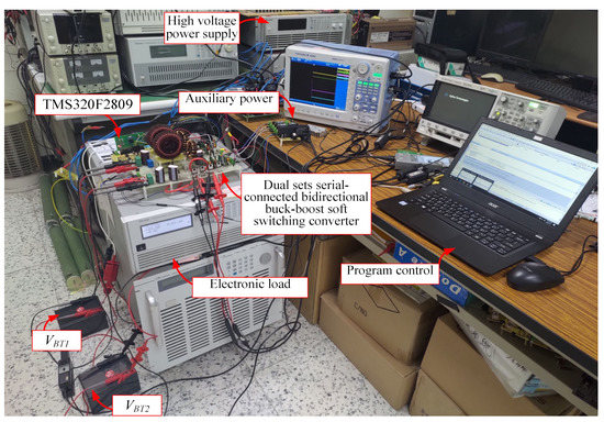
Figure 10.
Hardware circuit architecture of battery energy storage system with uniform charge and discharge.
Table 4.
The different output power rates of the photovoltaic module, the initial voltage of each set of batteries, and the final voltage after reaching uniform charging and discharging state.
Figure 11, Figure 12, Figure 13 and Figure 14 show the actual tested waveforms when the output power rates of the photovoltaic module were 150 W and 200 W, and the battery discharges the load end uniformly. Figure 15, Figure 16, Figure 17 and Figure 18 show the output power of the photovoltaic module when the output power rates were 300 W and 400 W, respectively, and actual tested waveform under the uniform charging control of the photovoltaic module on the battery end. It can be observed from Figure 11, Figure 12, Figure 13 and Figure 14 that when the photovoltaic module output power (Ppv) was greater than the load power, the battery was charged; on the contrary, it can be observed from Figure 15, Figure 16, Figure 17 and Figure 18 that if the photovoltaic module output power (Ppv) was lower than the load power, the battery discharged to keep the DC link voltage (VH) constant. If the voltage difference between the two batteries was greater, the required uniform charge and discharge time were relatively longer, and the higher voltage battery had a larger discharge current in the initial stage of discharge; on the contrary, in the initial stage of charging, the higher the voltage, then the relatively lower the charging current of the battery. It can be observed from Figure 12, Figure 14, Figure 16 and Figure 18 that when the uniform charge and discharge control were completed, the voltages of the two batteries were the same, and the charge and discharge currents were also the same, so the goal of uniform charge and discharge was achieved.
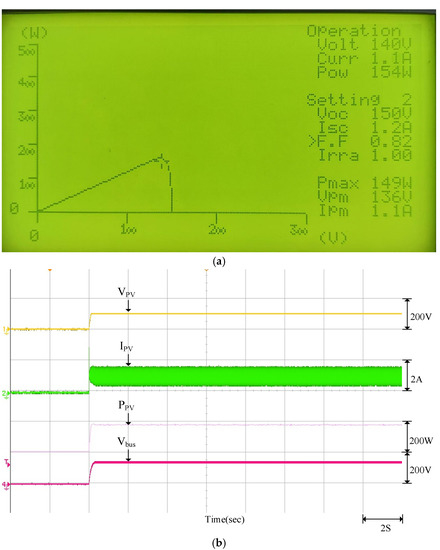
Figure 11.
Under the maximum power tracking when the photovoltaic module outputs 150 W: (a) P–V characteristic curve diagram; (b) actual tested waveform.
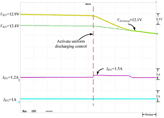
Figure 12.
When VBT1 = 12.9 V, VBT2 = 12.4 V, uniform discharge control response.
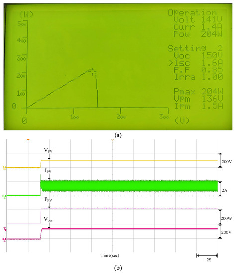
Figure 13.
Under maximum power tracking when the photovoltaic module outputs 200 W: (a) P–V characteristic curve diagram; (b) actual tested waveform.
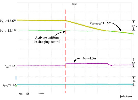
Figure 14.
When VBT1 = 12.6 V, VBT2 = 12.1 V, the uniform discharge control response.
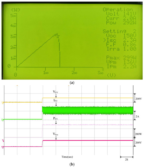
Figure 15.
Under the maximum power tracking when the photovoltaic module outputs 300 W: (a) P–V characteristic curve diagram; (b) actual tested waveform.
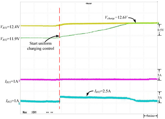
Figure 16.
When VBT1 = 12.4 V, VBT2 = 11.9 V, uniform charge control response.
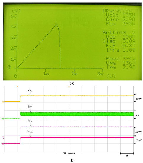
Figure 17.
Under the maximum power tracking when the photovoltaic module outputs 400 W: (a) P–V characteristic curve diagram; (b) actual tested waveform.
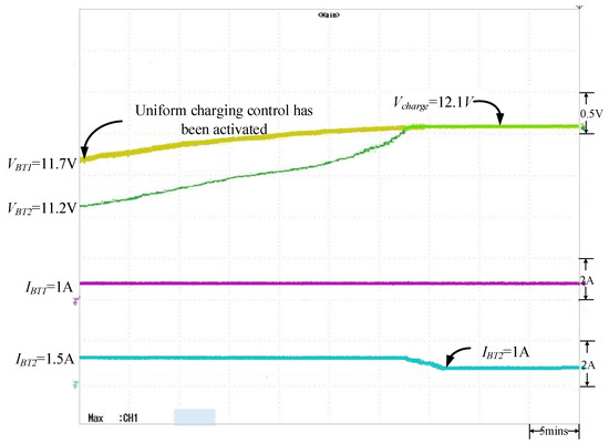
Figure 18.
The uniform charge control response when VBT1 = 11.7 V and VBT2 = 11.2 V.
The experiment results show that the conventional proportional integral (PI) controller parameters of the battery’s charging and discharging voltage and current will affect the battery’s uniform charging and discharging speed. Thus, to achieve the expected charging and discharging response, a quantitative design will be implemented for the controller in the next stage. In addition, because the battery’s charging and discharging rates affect the battery’s uniform charging and discharging time, if the maximum charging and discharging current in the original setting is not changed and a larger capacity battery is used, the uniform charging and discharging times will become longer.
6. Conclusions
This work takes the energy storage system architecture of a battery with uniform charge and discharge control combined with a photovoltaic module array as the research topic. Firstly, we developed the bidirectional buck–boost converter used and performed the performance measurement of the converter under loads of 50 W to 300 W. Then, the two sets of converters were serial-connected to construct an architecture with uniform charging and discharging. The TMS320F2809 digital signal processor was used as the control core, with the photovoltaic module and its maximum power tracking technology. The battery charging and discharging control was planned according to the strategic plan that the battery can achieve uniform charge and discharge. Two sets of batteries with different voltages were used for uniform charge and discharge control during the actual test. The actual test results verify that the adopted uniform charge and discharge control strategy can indeed achieve the uniform charge and discharge control effect of the battery. To improve the power imbalance problem during the battery charging and discharging process, and to prevent overcharge and over-discharge, the charging and discharging circuit used in this work has a soft-switching function. Compared to a traditional hard-switching circuit, this has a lower switching loss. This increases the efficiency by nearly 4% when the charging and discharging circuit load power is above 125 W. However, the energy storage equipment used in this work were lead-acid batteries, which cost less but create higher environmental pollution. Thus, future studies can use lithium batteries or lithium-ion batteries instead of lead-acid batteries. Alternatively, retired electric car batteries can be used to lower the cost of the energy storage system so that the energy storage system can be more flexible. Furthermore, the uniform charging and discharging architecture proposed for this work only detects the battery’s voltage and current and can only determine whether the battery’s charging and discharging electrical power is uniform. This work did not include state of charge (SOC) and state of health (SOH) testing, and cannot monitor battery power quantity and health. Thus, a battery management system (BMS) can be added in the future to improve battery use efficiency and extend battery life.
Author Contributions
K.-H.C. planned the project and carried out the writing, editing, and review. He also performed the analysis and optimized the charge/discharge control algorithm. B.-Z.H. and J.-J.J. were responsible for the data curation, software, and experimental corroboration for the maximum power point tracker and bidirectional buck–boost soft-switching converters. K.-H.C. administered the project. All authors have read and agreed to the published version of the manuscript.
Funding
The authors gratefully acknowledge the support and funding of this project by the Ministry of Science and Technology, Taiwan, under Grant Number MOST 108-2622-E-167-018–CC3.
Institutional Review Board Statement
Not applicable.
Informed Consent Statement
Not applicable.
Data Availability Statement
This study did not report any data.
Conflicts of Interest
The authors declare no conflict of interest.
References
- Georgious, R.; Refaat, R.; Garcia, J.; Daoud, A.A. Review on Energy Storage Systems in Microgrids. Electronics 2021, 10, 2134. [Google Scholar] [CrossRef]
- Portalo, J.M.; González, I.; Calderón, A.J. Monitoring System for Tracking a PV Generator in an Experimental Smart Microgrid: An Open-Source Solution. Sustainability 2021, 13, 8182. [Google Scholar] [CrossRef]
- Zhang, N.; Yang, N.C.; Liu, J.H. Optimal Sizing of PV/Wind/Battery Hybrid Microgrids Considering Lifetime of Battery Banks. Energies 2021, 14, 6655. [Google Scholar] [CrossRef]
- Koseoglou, M.; Tsioumas, E.; Jabbour, N.; Mademlis, C. Highly effective cell equalization in a lithium-ion battery management system. IEEE Trans. Power Electron. 2020, 35, 2088–2099. [Google Scholar] [CrossRef]
- Lozano, J.G.; Cadaval, E.R.; Montero, M.I.M.; Martinez, M.A.G. Battery equalization active methods. J. Power Sources 2014, 246, 934–949. [Google Scholar] [CrossRef]
- Kelkar, A.; Dasari, Y.; Williamson, S.S. A comprehensive review of power electronics enabled active battery cell balancing for smart energy management. In Proceedings of the 2020 IEEE International Conference on Power Electronics, Smart Grid and Renewable Energy (PESGRE2020), Cochin, India, 2–4 January 2020; pp. 1–6. [Google Scholar]
- Hoque, M.M.; Hannan, M.A.; Mohamed, A.; Ayob, A. Battery charge equalization controller in electric vehicle applications: A review. Renew. Sust. Energ. Rev. 2017, 75, 1363–1385. [Google Scholar] [CrossRef]
- Ye, Y.; Cheng, K.W.E.; Fong, Y.C.; Xue, X.; Lin, J. Topology, modeling, and design of switched-capacitor-based cell balancing systems and their balancing exploration. IEEE Trans. Power Electron. 2017, 32, 4444–4454. [Google Scholar] [CrossRef]
- Ye, Y.; Cheng, K.W.E. Analysis and design of zero-current switching switched-capacitor cell balancing circuit for series-connected battery/supercapacitor. IEEE Trans. Veh. Technol. 2018, 67, 948–955. [Google Scholar] [CrossRef]
- Caspar, M.; Eiler, T.; Hohmann, S. Systematic comparison of active balancing: A model-based quantitative analysis. IEEE Trans. Veh. Technol. 2018, 67, 920–934. [Google Scholar] [CrossRef]
- Shang, Y.; Lu, F.; Xia, B.; Zhang, C.; Cui, N.; Mi, C. A switched-coupling-capacitor equalizer for series-connected battery strings. In Proceedings of the 2017 IEEE Applied Power Electronics Conference and Exposition (APEC), Tampa, FL, USA, 26–30 March 2017; pp. 1425–1429. [Google Scholar]
- Zhou, Z.; Shang, Y.; Duan, B.; Zhang, C. An any-cell(s)-to-any-cell(s) equalizer based on bidirectional inductor converters for series connected battery string. In Proceedings of the 2016 IEEE 11th Conference on Industrial Electronics and Applications (ICIEA), Hefei, China, 5–7 June 2016; pp. 2511–2515. [Google Scholar]
- Dong, Y.; Li, F.; Li, W.; Wei, H. Voltage equalization optimization strategy for storage battery of power grid. In Proceedings of the 2021 IEEE 5th Information Technology, Networking, Electronic and Automation Control Conference (ITNEC), Xi’an, China, 15–17 October 2021; pp. 26–32. [Google Scholar]
- Lu, C.; Kang, L.; Wang, S. A novel symmetrical extensible battery balancing circuit based on inductor. In Proceedings of the 2018 21st International Conference on Electrical Machines and Systems (ICEMS), Jeju, Korea, 7–10 October 2018; pp. 2133–2136. [Google Scholar]
- Daowd, M.; Omar, N.; Bossche, P.V.D.; Mierlo, J.V. Passive and active battery balancing comparison based on MATLAB simulation. In Proceedings of the 2011 IEEE Vehicle Power and Propulsion Conference, Chicago, IL, USA, 6–9 September 2011; pp. 1–7. [Google Scholar]
- Li, Y.; Xu, J.; Mei, X.; Wang, J. A unitized multiwinding transformer-based equalization method for series-connected battery strings. IEEE Trans. Power Electron. 2019, 34, 11981–11989. [Google Scholar] [CrossRef]
- Shang, Y.; Cui, N.; Zhang, C. An optimized any-cell-to-any-cell equalizer based on coupled half-bridge converters for series-connected battery strings. IEEE Trans. Power Electron. 2019, 34, 8831–8841. [Google Scholar] [CrossRef]
- Zheng, L.; Zhu, J.; Wang, G.; Lu, D.D.C.; McLean, P.; He, T. Model predictive control based balancing strategy for series-connected lithium-ion battery packs. In Proceedings of the 2017 19th European Conference on Power Electronics and Applications (EPE’17 ECCE Europe), Warsaw, Poland, 11–14 September 2017; pp. 1–8. [Google Scholar]
- Shin, J.W.; Seo, G.S.; Chun, C.Y.; Cho, B.H. Selective flyback balancing circuit with improved balancing speed for series connected lithium-ion batteries. In Proceedings of the 2010 International Power Electronics Conference–ECCE ASIA, Sapporo, Japan, 21–24 June 2010; pp. 1180–1184. [Google Scholar]
- Li, S.; He, J.; Guo, Z. A novel lithium-ion battery active equalization structure and its control strategy based on buck converter unit. In Proceedings of the 2018 IEEE International Power Electronics and Application Conference and Exposition (PEAC), Shenzhen, China, 4–7 November 2018; pp. 1–5. [Google Scholar]
- Jangir, P.; Sangwan, V.; Kumar, R.; Rathore, A.K. Optimal power management of multiple battery units by power converter system in electric vehicle. In Proceedings of the 2018 IEEE International Conference on Power Electronics, Drives and Energy Systems (PEDES), Chennai, India, 18–21 December 2018; pp. 1–6. [Google Scholar]
- Femia, N.; Granozio, D.; Petrone, G.; Spagnuolo, G.; Vitelli, M. Predictive and adaptive MPPT perturb and observe method. IEEE Trans. Aerosp. Electron. Syst. 2007, 43, 934–950. [Google Scholar] [CrossRef]
- Femia, N.; Lisi, G.; Petrone, G.; Spagnuolo, G.; Vitelli, M. Distributed maximum power point tracking of photovoltaic arrays: Novel approach and system analysis. IEEE Trans. Ind. Electron. 2008, 55, 2610–2621. [Google Scholar] [CrossRef] [Green Version]
- Chao, K.H.; Huang, C.H. Bidirectional DC–DC soft-switching converter for stand-alone photovoltaic power generation systems. IET Power Electron. 2014, 7, 1557–1565. [Google Scholar] [CrossRef]
- Jian, J.J. Energy Storage System with Uniform Battery Charging and Discharging Control. Master Thesis, National Chin-Yi University of Technology, Taichung City, Taiwan, 23 July 2020. [Google Scholar]
- Texas Instruments TMS320F2809 Datasheet. Available online: https://www.ti.com/lit/ds/symlink/tms320f2809.pdf?ts=1594465026502&ref_url=https%253A%252F%252Fwww.ti.com%252Fproduct%252FTMS320F2809.pdf (accessed on 12 November 2021).
- Scarabaggio, P.; Carli, R.; Cavone, G.; Dotoli, M. Smart Control Strategies for Primary Frequency Regulation through Electric Vehicles: A Battery Degradation Perspective. Energies 2020, 13, 4586. [Google Scholar] [CrossRef]
- Yan, G.; Liu, D.; Li, J.; Mu, G. A cost accounting method of the Li-ion battery energy storage system for frequency regulation considering the effect of life degradation. Prot. Control Mod. Power Syst. 2018, 3, 4. [Google Scholar] [CrossRef]
- Carli, R.; Dotoli, M. A Distributed Control Algorithm for Optimal Charging of Electric Vehicle Fleets with Congestion Management. IFAC-PapersOnLine 2018, 51, 373–378. [Google Scholar] [CrossRef]
- Hoke, A.; Brissette, A.; Smith, K.; Pratt, A.; Maksimovic, D. Accounting for Lithium-Ion Battery Degradation in Electric Vehicle Charging Optimization. IEEE J. Emerg. Sel. Top. Power Electron. 2014, 2, 691–700. [Google Scholar] [CrossRef]
Publisher’s Note: MDPI stays neutral with regard to jurisdictional claims in published maps and institutional affiliations. |
© 2022 by the authors. Licensee MDPI, Basel, Switzerland. This article is an open access article distributed under the terms and conditions of the Creative Commons Attribution (CC BY) license (https://creativecommons.org/licenses/by/4.0/).