Article

Impedance Modeling and Stability Analysis of Three-Phase Four-Wire Inverter with Grid-Connected Operation

College of Electrical Engineering, Navel University of Engineering, JieFang Road 717, Wuhan 430000, China
*
Author to whom correspondence should be addressed.
Energies 2022, 15(8), 2754; https://doi.org/10.3390/en15082754
Submission received: 11 February 2022 / Revised: 26 March 2022 / Accepted: 2 April 2022 / Published: 8 April 2022
(This article belongs to the Section F: Electrical Engineering)

Abstract

:
With the continuous penetration and development of renewable energy power generation, distributed grids and microgrids are becoming increasingly important in power systems. In the distribution networks and microgrids, the grid impedance is comparatively large and cannot be ignored. Usually, the parallel compensation is used to improve the grid quality. In these three-phase four-wire power systems, analyzing the impedance characteristics of the grid-connected inverter is vital to carry out the small-signal stability analysis. Thus, it is vital to consider the influence of the zero-sequence component in addition to the positive-sequence component and the negative-sequence component when it comes to analyzing system stability. In this paper, the impedances of three-phase four-wire split capacitor inverter and three-phase four-leg inverter are established. Based on the achieved impedance, the similarities and differences between the impedances of three-phase four-wire split capacitor inverter and impedance of three-phase four-leg inverter are studied. The main difference is reflected in zero-sequence impedance. Additionally, the zero-sequence impedance characteristics and the dominating factors deciding the zero-sequence impedance are analyzed. Then, the stability of the system considering the grid impedance and impedance of three-phase four-wire inverter is investigated by separately considering the stability of the positive–negative-sequence component and the stability of the zero-sequence component. Several cases of small-signal instability caused by the positive–negative-sequence component or zero-sequence component are revealed. The experimental results validate the theoretical analysis.

1. Introduction

With the continuous penetration and development of renewable energy power generation, distribution networks and microgrids account for an increasing proportion of contemporary power grids [1,2,3]. In distribution networks and microgrids, the three-phase four-wire system has been widely promoted and applied [4,5,6,7,8,9], because it can provide a zero-sequence current path and is suitable for both symmetrical and asymmetrical conditions. In the three-phase four-wire system, the three-phase four-wire inverter has important functions such as power transmission and power quality improvement devices. The three-phase four-wire split capacitor inverter (TFSCI) and three-phase four-leg inverter (TFGI) have been widely used due to their low cost, simple control, and small size. Their application scenarios include islanded microgrid [4], active filter [5], power redistribution device [6], renewable energy power generation system [7], uninterruptible power supply [8], and power distribution system [9].
Because the distribution network and microgrid are usually weak grids with large impedance, parallel compensation capacitors are typically equipped to perform reactive power compensation and harmonic filtering to improve voltage quality and enlarge power transmission capacity [10,11,12]. Therefore, it is a very common scenario in a three-phase four-wire system that the three-phase four-wire inverter connects to a weak grid with parallel compensation capacitors.
When the three-phase four-wire inverter connects to the grid whose impedance cannot be neglected, the interactions between the inverter systems and weak grid may cause stability issues. Many methods can be used to analyze the characteristics of system stability. These methods include the loop-gain method [13,14,15], eigenvalues analysis based on system state-space method [16], the passivity method [17,18], and the impedance-based method [19,20,21,22,23,24,25].
Among these analytical methods, the impedance-based analysis method is proved as an effective way to study and resolve the small-signal instability problems caused by the interaction between the converter and the grid [21,22,23,24,25]. A stability criterion for grid-connected inverters based on Gershgorin’s theorem and impedance model is proposed in [21]. Reference [22] establishes the entire impedance of RSC and VSC considering coupling factors to analyze the system stability. In [23], a single-in-single-out impedance model of grid-connected inverters with a virtual synchronous generator using a cascaded inner control loop is established to analyze the system stability under different kinds of weak grids.
The small-signal instability problems of the three-phase three-wire grid-connected inverter system have received wide attention and research, and numerous meaningful conclusions have been achieved. However, these conclusions cannot accurately reflect the stability of three-phase four-wire grid-connected inverter system because the zero-sequence component is not considered. The zero-sequence component is also a factor that will cause the small-signal instability of the system except the negative-sequence and the positive-sequence components.
To analyze the small-signal stability of the three-phase four-wire system including zero-sequence stability by the analysis method based on impedance, the impedance of the three-phase four-wire inverter should be achieved firstly. By analyzing the transmission path of the zero-sequence, positive-sequence, and negative-sequence small-signals perturbation in each sequence loop considering all the control blocks, the relationship between the small signal perturbation and the corresponding response in the frequency domain will be achieved as an impedance model of the inverter.
The derivation process of the impedance model including the zero-sequence impedance, positive-sequence impedance, and negative-sequence impedance is much more complex than that of the three-phase three-wire inverter impedance model. The matrix dimension increases from two-dimensional to three-dimensional, and the effect of the zero-sequence component on the disturbance loop should be considered. Then, the small-signal instability issue can be studied on the basis of the obtained impedance model. When performing stability analysis, it is not only necessary to consider the stability of the positive and negative sequences, but also to consider whether the zero-sequence impedance will bring stability problems, which increases the complexity of the analysis process.
Additionally, based on the obtained impedance model, the impedance characteristics of TFSCI and TFGI are analyzed in this paper. The small-signal stability of TFSCI and TFGI are analyzed, and the instability cases are given in the weak grid and weak grid with parallel compensation.
The structure of the paper is organized as follows. Section 2 gives the system description and impedance models of TFSCI and TFGI. Then, the comparison of impedance characteristics between TFSCI and TFGI is presented in Section 3. The stability analyses of TFSCI and TFGI are studied in Section 4. The validity of the established impedance and stability analysis method are verified by experiments in Section 5. Section 6 concludes this paper.

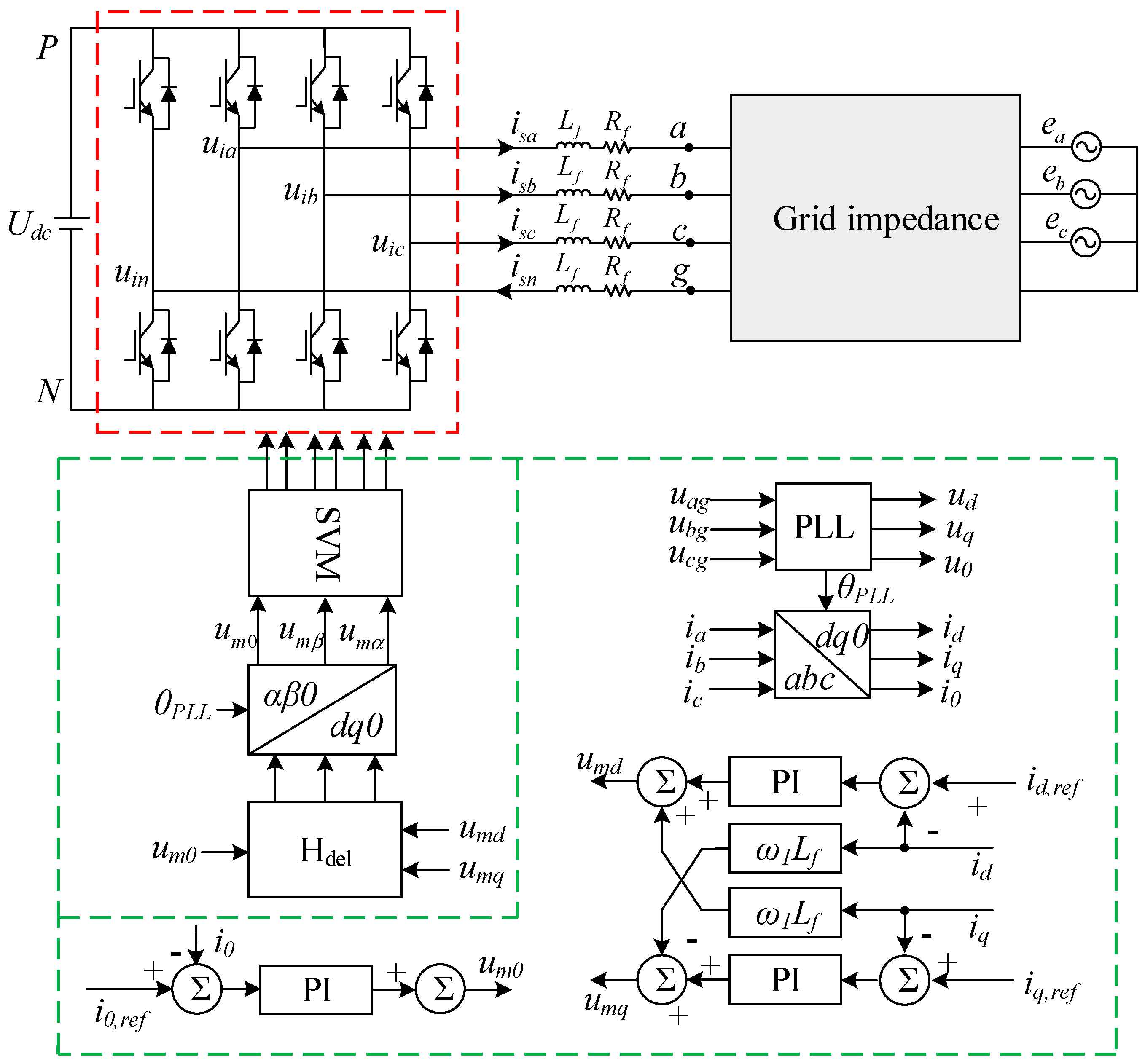
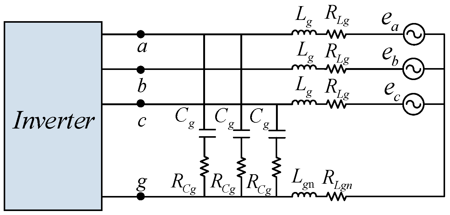
2. System Description and Impedance Modeling of TFSCI and TFGI

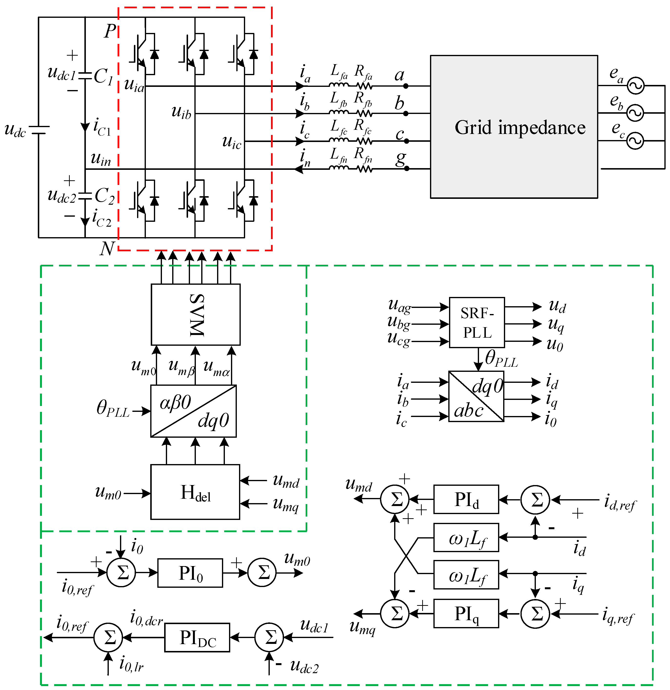
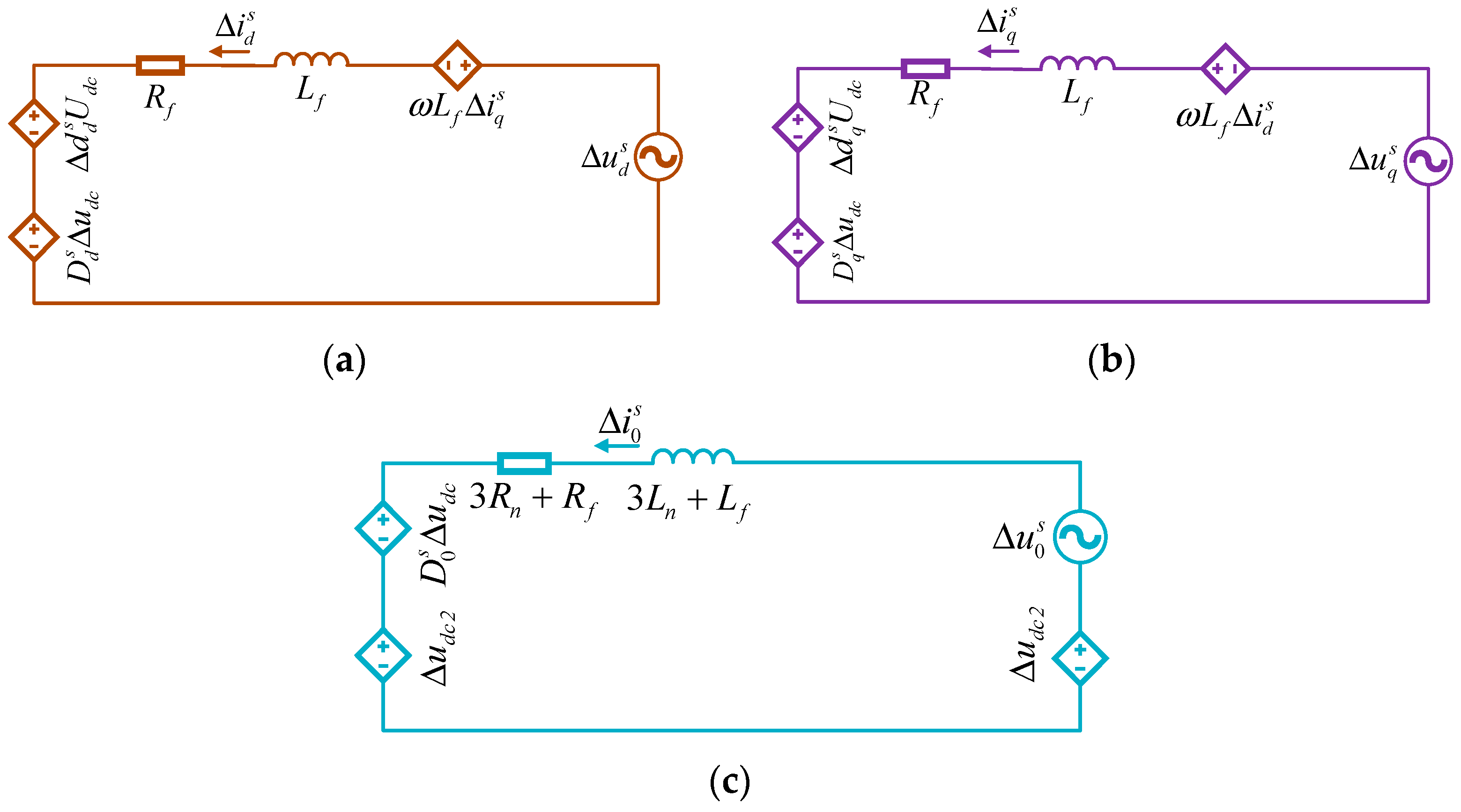
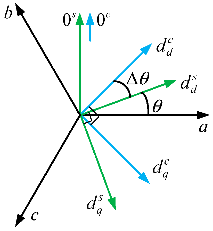
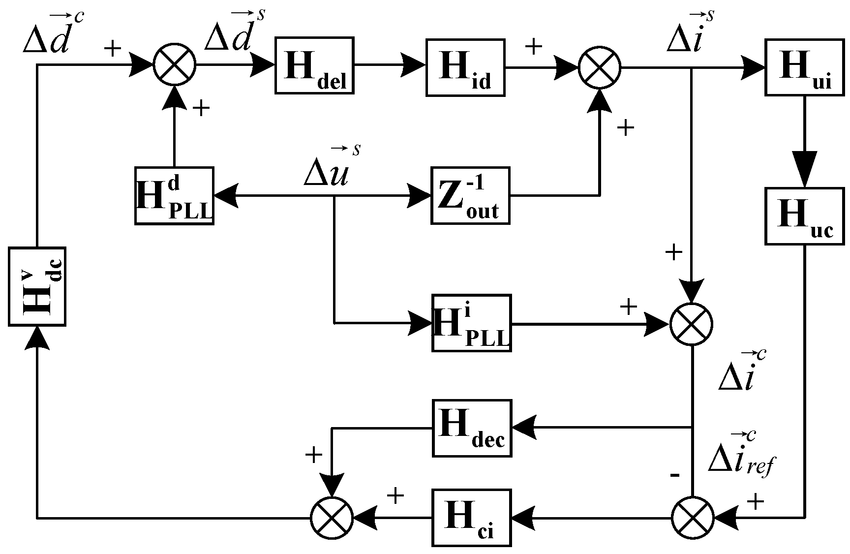
2.1. Impedance Modeling of TFSCI

The block diagram of TFSCI connected to the parallel compensation grid is shown in Figure 1. In Figure 1, Lfa, Lfb, Lfc, and Lfn represent the filter inductors; Rfa, Rfb, Rfc, and Rfn represent corresponding parasitic resistances. C1 and C2 are the DC-side capacitors, where C1 = C2 = Cdc. In Figure 1, the SRF-PLL is the synchronous reference frame phase-locked loop to achieve the synchronous angle of the grid. Based on the achieved angle, the currents and voltage in the dq0-domain can be obtained by the Park transformation. The PI controllers PId, PIq, and PI0 are used to control the d-axis, q-axis, and 0-axis currents, respectively. The PI controller PIDC is used to balance the DC voltage of C1 and C2.
The voltages in each leg of the TFSCI, measured from the negative point of the DC-link N, can be obtained as,
[ u a N u b N u c N ] = [ S a S b S c ] u d c
where Sa, Sb, and Sc are the signals used to control the switching states.
According to (1), the phase voltage can be expressed as,
[ u a n u b n u c n ] = [ u a N u n N u b N u n N u c N u n N ] [ u d c 2 u d c 2 u d c 2 ] = [ d a d b d c ] u d c [ u d c 2 u d c 2 u d c 2 ]
where d a ,   d b ,   d c are the duty ratios of phase a, phase b, and phase c, respectively.
From Figure 1, under the assumption that L f a = L f b = L f c = L f , R f a = R f b = R f c = R f , L f n = L n , R f n = R n , through Kirchhoff’s voltage law, the voltages in the three-phase domain can be written as,
[ u a n u b n u c n ] = [ L f a 0 0 0 L f b 0 0 0 L f c ] [ p i a p i b p i c ] + [ R f a 0 0 0 R f b 0 0 0 R f c ] [ i a i b i c ] + L f n [ p i n p i n p i n ] + R f n [ i n i n i n ] + [ u a g u b g u c g ]
where p represents the differential operator d/dt.
Through Kirchhoff’s current law, the zero-sequence current can be written as,
i 0 = C f 3 d ( u c 2 u c 1 ) d t
Practically, the circuit model is usually converted to the dq0 coordinate system to achieve decoupling control of active and reactive currents. The synchronous reference frame phase-locked loop (SRF-PLL) is extensively used to obtain the coordinate transformation angle θ between the three-phase frames and the dq0 frames. The block diagram of SRF-PLL is shown in Figure 2.
Then, with joints (2) and (3), through the Park transformation, the mathematical model in the system dq0 frame can be obtained as,
[ d d d q d 0 ] u d c = [ L f 0 0 0 L f 0 0 0 3 L n + L f ] [ p i d p i q p i 0 ] + [ R f 0 0 0 R f 0 0 0 3 R n + R f ] [ i d i q i 0 ] + [ 0 ω L f 0 ω L f 0 0 0 0 0 ] [ i d i q i 0 ] + [ u d u q u 0 ] [ 0 0 u d c 2 ]
In Equation (5), p is the differential operator d/dt.
From Figure 3, assuming Δ d d s = Δ d q s = Δ d 0 s , the transfer function matrix from perturbation voltage to current response in the system frame can be expressed as,
Z S C o u t = [ s L f + R f ω L f 0 ω L f s L f + R f 0 0 0 s ( L f + 3 L n ) + R f + 3 R n 3 2 s C ]
The ‘s’ represents the Laplace operator in Equation (6). The detailed derivation process can be seen in Appendix A.
The small-signal model from (5) can be derived. Figure 4 shows its equivalent circuit in which X is the steady-state value of X, and Δx represents the small-signal perturbation. Note that the small-signal model is established on the quiescent operation point.
Similarly, in Figure 3, assuming Δ u d s = Δ u q s = Δ u q s = 0 , the transfer function matrix from duty ratio perturbance to the corresponding current response can be expressed as,
H S C i d = [ ( s L f + R f ) U d c ( s L f + R f ) 2 + ( ω L f ) 2 ω L f U d c ( s L f + R f ) 2 + ( ω L f ) 2 0 ω L f U d c ( s L f + R f ) 2 + ( ω L f ) 2 ( s L f + R f ) U d c ( s L f + R f ) 2 + ( ω L f ) 2 0 0 0 U d c s ( 3 L n + L f ) + 3 R n + R f 3 2 s C ]
Because of the dynamic performance of SRF-PLL, harmonic voltages will bring about corresponding phase perturbation, leading to an angular difference Δθ between the controller dq0dq0 frame and system dq0dq0 frame in the d-axis and q-axis except 0-axis. In this paper, the variable in the controller dq0dq0 frame is defined as Xc with superscript c while Xs with superscript s is in the system dq0 frame. The relationship between the controller and system dq0 frames can be seen in Figure 4.
From Figure 2, Δθ can be obtained as,
Δ θ = Δ u q c ( k p p + k i p s ) 1 s
The conversion of the variables in the system dq0-domain to the controller dq0-domain can be obtained as,
X c = [ cos ( Δ θ ) sin ( Δ θ ) 0 sin ( Δ θ ) cos ( Δ θ ) 0 0 0 1 ] X s
Introducing the perturbation, the relationships between U c and U s , and I c and I s in the small-signal model can be expressed as:
[ U d c + Δ u d c U q c + Δ u q c U 0 c + Δ u 0 c ] = [ cos ( Δ θ ) sin ( Δ θ ) 0 sin ( Δ θ ) cos ( Δ θ ) 0 0 0 1 ] [ U d s + Δ u d s U q s + Δ u q s U 0 s + Δ u 0 s ]
[ I d c + Δ i d c I q c + Δ i q c I 0 c + Δ i 0 c ] = [ cos ( Δ θ ) sin ( Δ θ ) 0 sin ( Δ θ ) cos ( Δ θ ) 0 0 0 1 ] [ I d s + Δ i d s I q s + Δ i q s I 0 s + Δ i 0 s ]
The Δθ is ignorable; then, (10) and (11) can be simplified as,
[ Δ u d c Δ u q c Δ u 0 c ] [ Δ u d s + U q s Δ θ Δ u q s U d s Δ θ Δ u 0 s ]
[ Δ i d c Δ i q c Δ i 0 c ] [ Δ i d s + I q s Δ θ Δ u q s I d s Δ θ Δ i 0 s ]
Combining (8) and (10), the relationship between Δθ and Δuqs can be expressed as,
Δ θ = k p p + k p i / s s + U d s ( k p p + k p i / s ) Δ u q s
Defining
H P L L = k p p + k i p / s s + U d s ( k p p + k i p / s )
Joining (12) to (11), the relationship between Δ u s can Δ i c be obtained as,
[ Δ i d c Δ i q c Δ i 0 c ] = [ 0 I q s H P L L 0 0 I d s H P L L 0 0 0 0 ] [ Δ u d s Δ u q s Δ u 0 s ]
Defining H P L L i as the matrix of Δ u s to Δ i c ,
H P L L i = [ 0 H P L L I q s 0 0 H P L L I d s 0 0 0 0 ]
Similarly, the matrix H P L L d of Δ u s to duty ratio perturbation can be obtained as,
H P L L d = [ 0 D q s H P L L 0 0 D q s H P L L 0 0 0 0 ]
The control block diagram, mainly including the DC voltage balance PI controller, the PLL, and the current PI controller, makes a great contribution to the performance of the system, which is necessary to be considered in the modeling process.
The block diagram of the impedance model of TFSCI can be seen in Figure 5. Matrix Hdel represents the control delay element, matrix Hdec represents the d-q decoupling term in the current controller, and matrix Hci represents the PI regulator in the current controller.
H d e c = [ 0 ω L f 0 ω L f 0 0 0 0 0 ]
H d c = [ 1 / U d c 0 0 0 1 / U d c 0 0 0 1 / U d c ]
H d e l = [ e T d e l s 0 0 0 e T d e l s 0 0 0 e T d e l s ]
H c i = [ k d i p + k d i i s 0 0 0 k q i p + k q i i s 0 0 0 k 0 i p + k 0 i i s ]
From (4), matrix Hui of the perturbation of current in the system dq0 frame to the perturbation of DC voltage can be expressed as,
H u i = [ 0 0 0 0 0 0 0 0 3 / 2 S C f ]
From Figure 1, in the DC voltage balance PI controller, the expression Gcu from the perturbation of DC voltage to the perturbation current reference can be obtained as,
G cu = [ 0 0 0 0 0 0 0 0 k d c p + k d c i / s ]
According to Figure 5, the admittance from Δ i s to Δ u s , or the admittance of TFSCI in the dq0-domian, can be obtained as,
Y S C d q 0 = H S C i d H d e l H d c ( H P L L i ( H d e c H c i ) ) + H S C i d H d e l ( H P L L d + ( H S C i d H d e l ) 1 Z o u t 1 ) I H S C i d H d e l H d c ( H d e c H c i ) G c u H c i H d c H u i H S C i d H d e l
In the actual system, the components in the pn0-domain are easier to measure than the components in the dq0-domian. Therefore, it is necessary to transform the impedances in the dq0-domain to the impedances in the pn0-domain. In the case of three-phase symmetrical conditions, reference [26] indicates that the admittance in the dq0-domain can be equivalently transformed into the sequence domain as,
Y SCpn 0 = T Z Y d q 0 T Z 1 = [ Y i p n 0 0 Y i 0 ] = [ Y 11 Y 12 0 Y 21 Y 22 0 0 0 Y 33 ]
T Z = 1 2 [ 1 j 0 1 j 0 0 0 2 ]

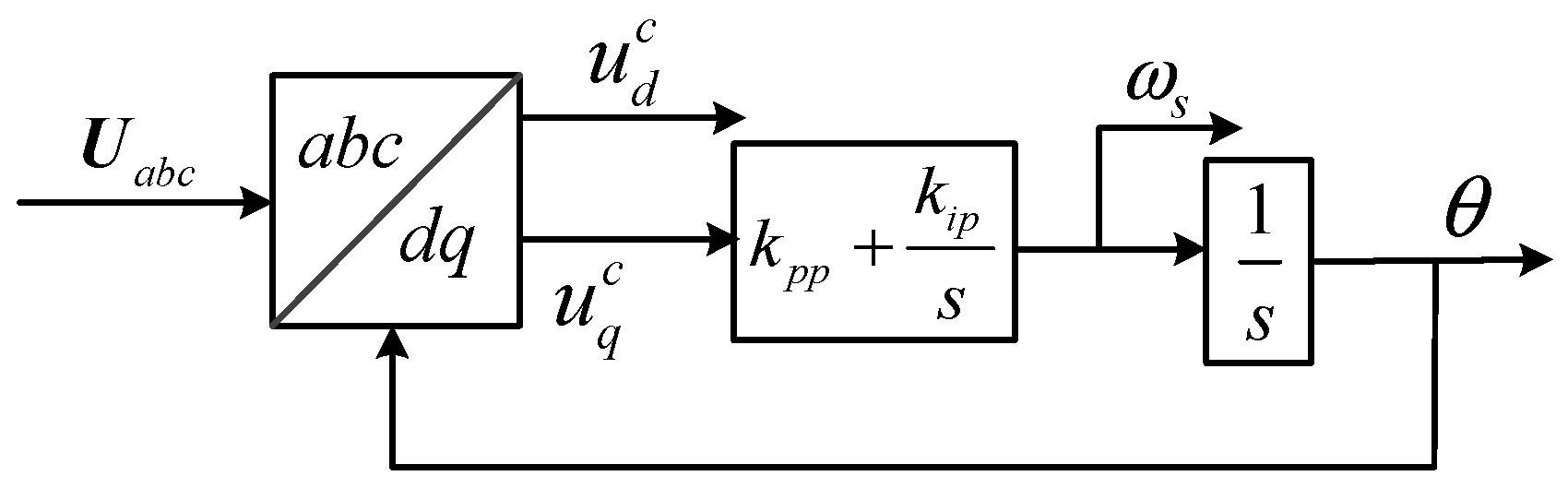
2.2. Impedance Modeling of the TFGI

The block diagram of the TFGI connected to the parallel compensation grid is shown in Figure 6. In Figure 1, Lf and Ln represent the filter inductor, and Rf and Rfn represent the corresponding parasitic resistance. Referring to the derivation process in Section 2.1, the admittance of TFGI in the dq0-domian can be expressed as [27],
Y FLpn 0 = T Z Y d q 0 T Z 1 = [ Y i p n 0 0 Y i 0 ] = [ Y 11 Y 12 0 Y 21 Y 22 0 0 0 Y 33 ]
T Z = 1 2 [ 1 j 0 1 j 0 0 0 2 ]
Y F L d q 0 = H i d H d e l H d c ( H P L L i ( H d e c H c i ) ) I H F L i d H d e l H d c ( H d e c H c i ) + H F L i d H d e l ( H P L L d + ( H F L i d H d e l ) 1 Z F L o u t 1 ) I H F L i d H d e l H d c ( H d e c H c i )
where
Z F L o u t = [ s L f + R f ω L f 0 ω L f s L f + R f 0 0 0 s ( L f + 3 L n ) + R f + 3 R n ]
H F L i d = [ ( s L f + R f ) U d c ( s L f + R f ) 2 + ( ω L f ) 2 ω L f U d c ( s L f + R f ) 2 + ( ω L f ) 2 0 ω L f U d c ( s L f + R f ) 2 + ( ω L f ) 2 ( s L f + R f ) U d c ( s L f + R f ) 2 + ( ω L f ) 2 0 0 0 U d c s ( 3 L n + L f ) + 3 R n + R f ]
It should be noted that the main contribution of paper [27] is to establish the impedance model of the three-phase four-leg inverter and verify the decoupling relationships between the zero-sequence component and the positive-sequence component as well as the negative-sequence component. Compared to paper [27], although the derivation process in this paper for positive-sequence impedance and negative-sequence impedance is similar, the derivation process for zero-sequence impedance is completely different due to the different zero-sequence path and zero-sequence current control strategy.
The MATLAB/Simulink simulation is implemented for the purpose of verifying the correctness of the established impedance model. The frequency scanning result and the established impedance model of TFSCI and TFGI are presented in Figure A1 in Appendix B. In Figure A1, Yij denotes the ith element in the jth column in the admittance matrix of TFSCI Y SCpn 0 and the admittance matrix of TFGI Y FLpn 0 . From Figure A1, the established impedance model matches the measurement result well, which indicates that the established impedance model is accurate.

3. Comparison of Impedance Characteristics between TFSCI and TFGI

According to Equations (26) and (28), the negative-sequence impedance and positive-sequence impedance of TFGI and TFSCI are the same, and are also similar to those of the three-phase three-wire inverter [21,22,23,24,25]. To avoid a repetitive discussion of similar content, a detailed analysis of the negative-sequence impedance and the positive-sequence impedance will not be presented in this article. In the three-phase four-wire inverter, the zero-sequence impedance is special compared to the three-phase three-wire inverter. Hence, the zero-sequence impedance characteristics of TFSCI and TFGI will be analyzed in this section.

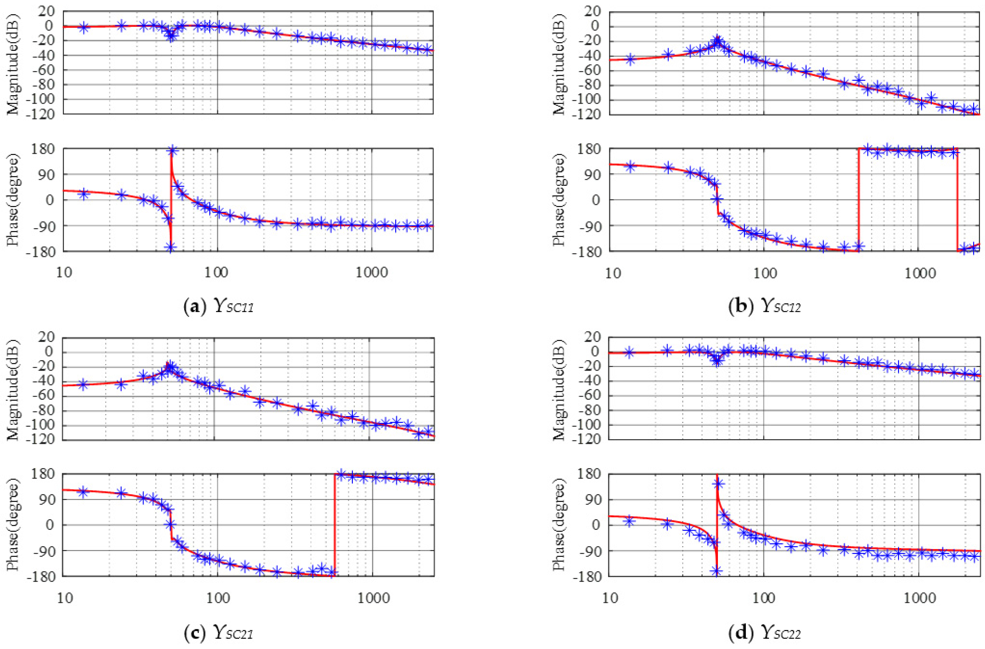
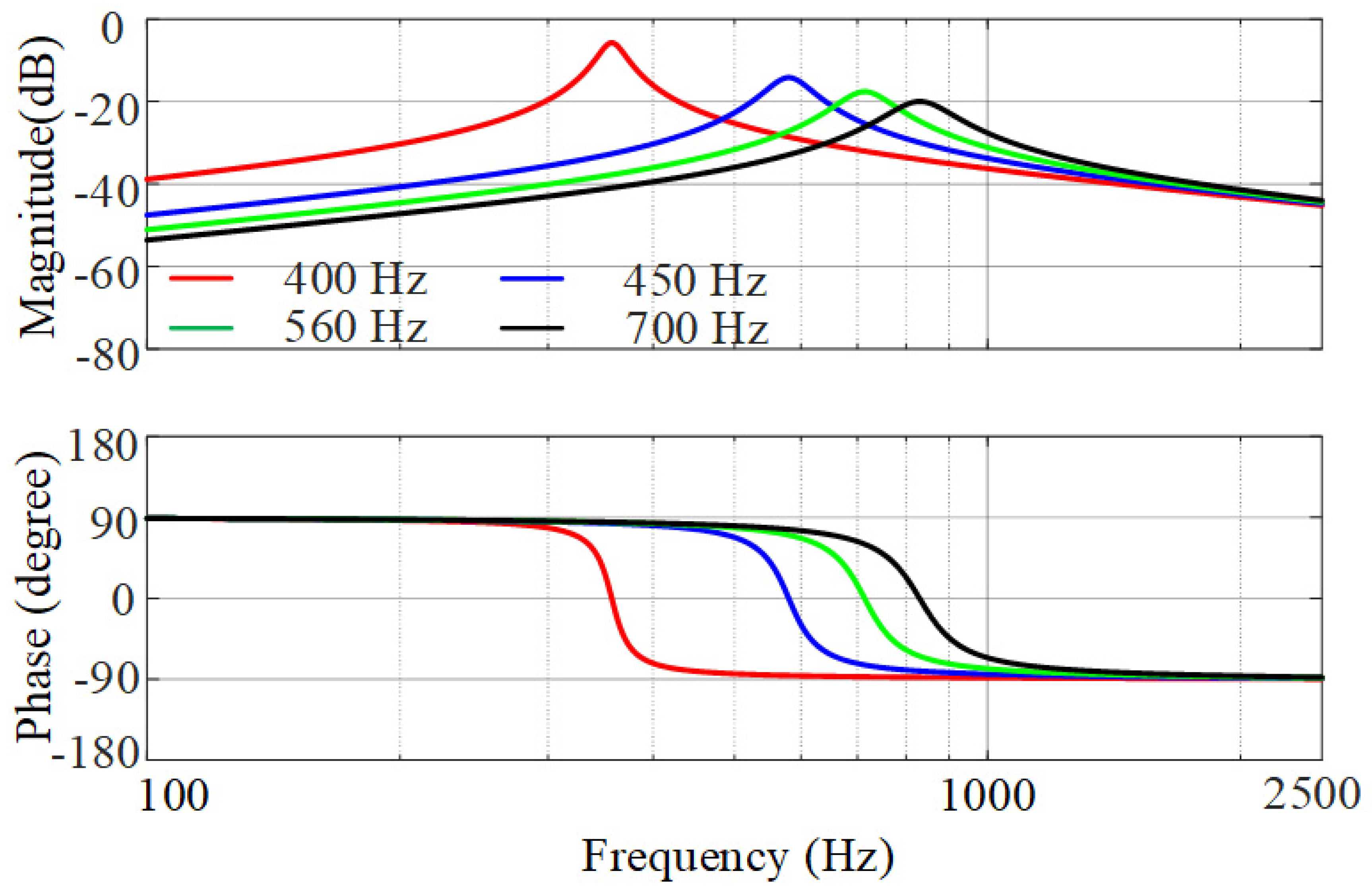
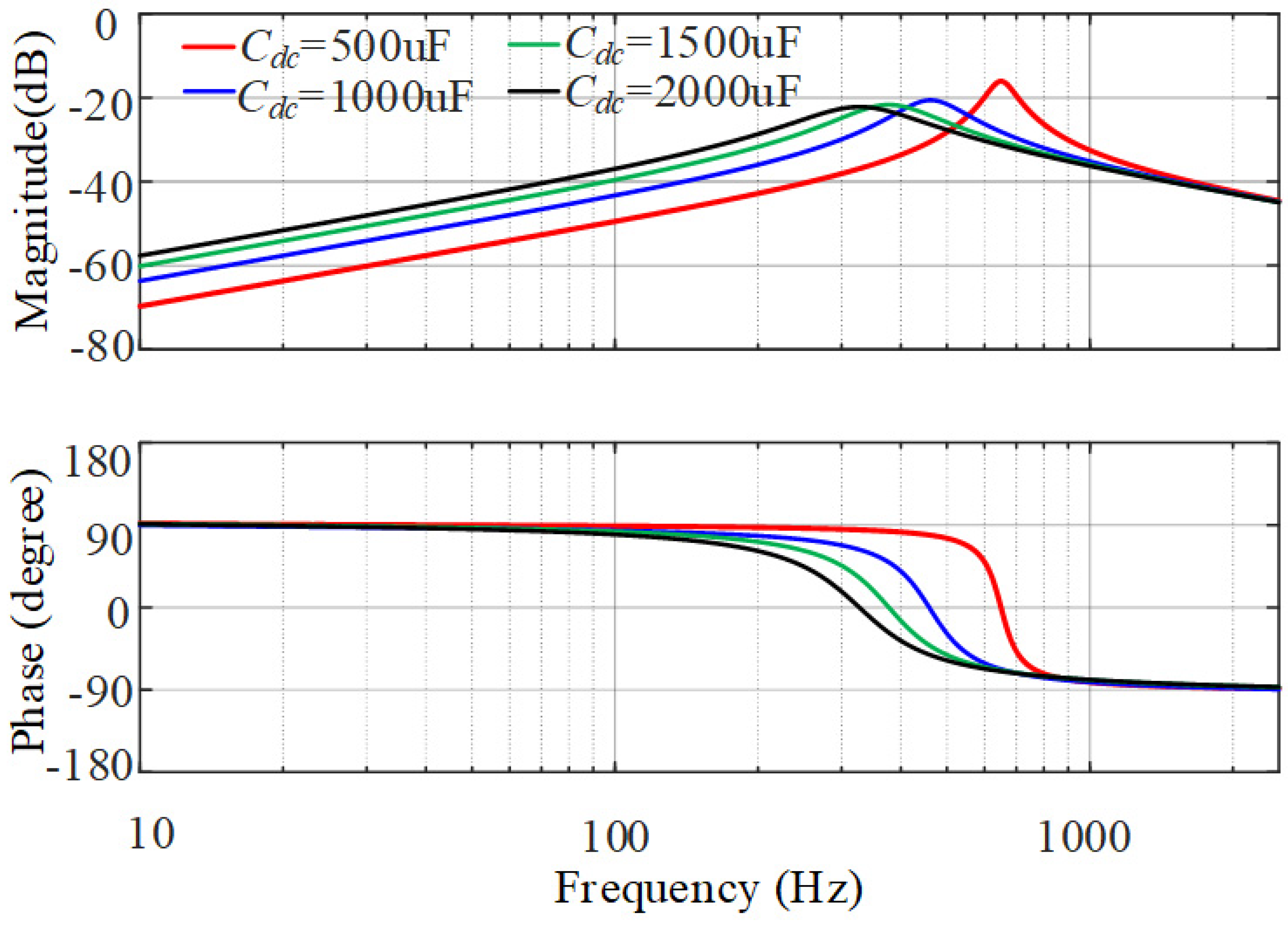
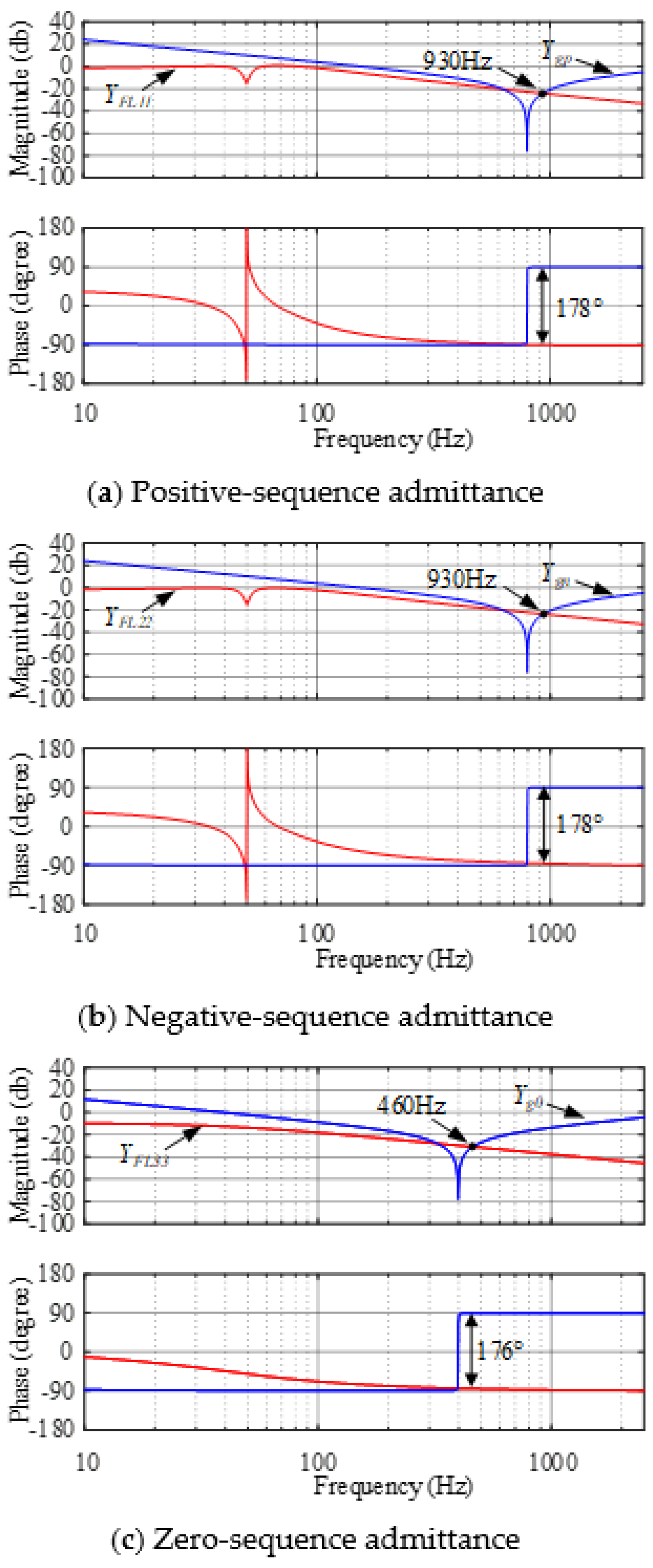
3.1. Zero-Sequence Impedance Characteristics of TFSCI

From (24), the zero-sequence admittance can be obtained as,
Y z _ T F S C I = 1 K m ( k 0 i p + k 0 i i / s + 3 2 s C d c ( k 0 v p + k 0 v i / s ) ) + s ( 3 L n + L f ) + 3 R n + R f
By organizing the above equation, the following equation can be obtained,
Y z _ T F S C I = 1 K m ( R z _ T F S C I + s L z _ T F S C I + 1 s ( C z _ T F S C I ) )
where
R z _ T F S C I = k 0 i p + 3 k 0 v i 2 C d c s 2 + 3 R n + R f L z _ T F S C I = 3 L n + L f C z _ T F S C I = 2 C d c 3 k 0 v p + 2 C d c k 0 i i
From (32), it shows that the zero-sequence admittance of TFSCI is relevant not only to the filter parameters and zero-sequence current controller parameters, but the DC voltage balance PI controller parameters and the DC-side capacitor as well. According to Equation (32), zero-sequence admittance will reach an amplitude peak when |sLz_TFSCI| = 1/|sCz_TFSCI|, and the value of the amplitude peak is decided by Rz_TFSCI according to Equation (32). An evident fact can be achieved that a larger Rz_TFSCI will bring a lower amplitude peak.
Figure 7 shows bode diagrams of TFSCI when different filter parameters are applied. As the filter inductance Lf and Ln increase, the amplitude peaks occur at lower frequencies. Under the same filter inductance, the zero-sequence admittance gradually transitions from inductive characteristics to capacitive characteristics as the frequency increases.
Figure 8 shows the zero-sequence admittance bode diagrams of TFSCI under different control bandwidths of the zero-sequence current controller. Under the same control bandwidth, the zero-sequence admittance gradually transitions from inductive characteristics to capacitive characteristics as the frequency increases. As the control bandwidth increases, the amplitude peak occurs at higher frequencies with lower amplitude due to a larger Rz_TFSCI and smaller Cz_TFSCI.
Figure 9 shows bode diagrams of the zero-sequence admittance of TFSCI when different DC-side capacitor Cdc values are applied. As the capacitor increases, the amplitude peak occurs at a lower frequency with lower amplitude. The reason is that the Cz_TFSCI and Rz_TFSCI will increase as Cdc increases. The larger Cz_TFSCI will lead the amplitude peak to occur at a lower frequency, and the larger Rz_TFSCI brings a lower amplitude peak and a wider transition zone from inductive characteristics to capacitive characteristics.
Figure 10 shows bode diagrams of the zero-sequence admittance of TFSCI under different voltage loop bandwidth used in the zero-axis DC voltage loop. It can be seen that the zero-sequence admittance gradually transitions from inductive characteristics to capacitive characteristics as the frequency increases. As the capacitor increases, the amplitude peak occurs at higher frequencies with higher amplitude. This is because the Cz_TFSCI and Rz_TFSCI will decrease as the control bandwidth increases. The smaller Cz_TFSCI will lead the amplitude peak to occur at a higher frequency and the smaller Rz_TFSCI brings a higher amplitude peak and a narrower transition zone from inductive characteristics to capacitive characteristics.

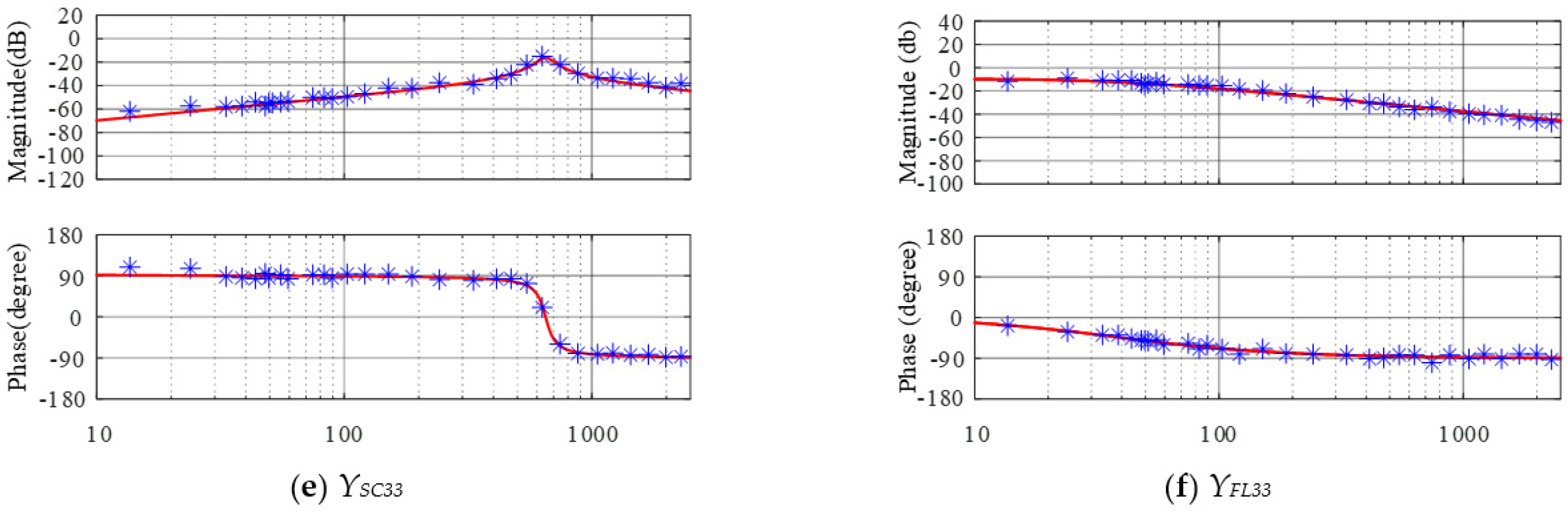
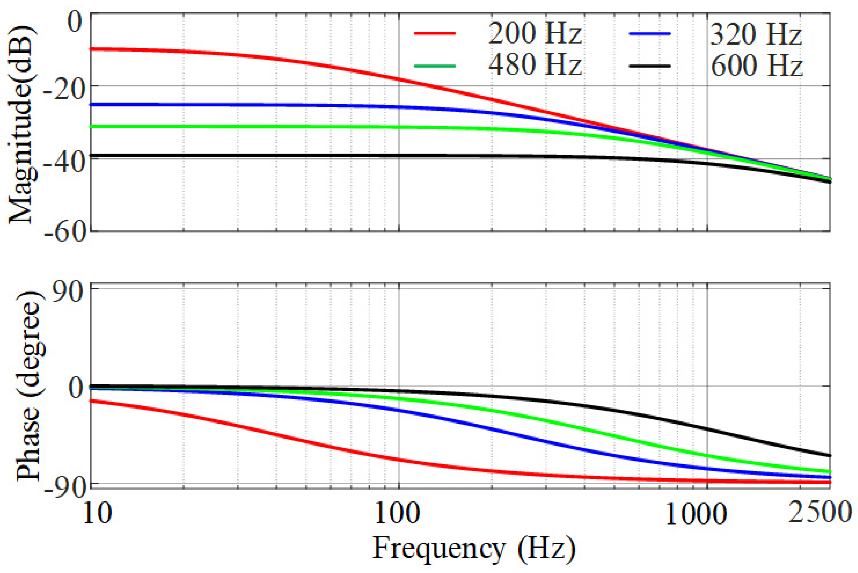
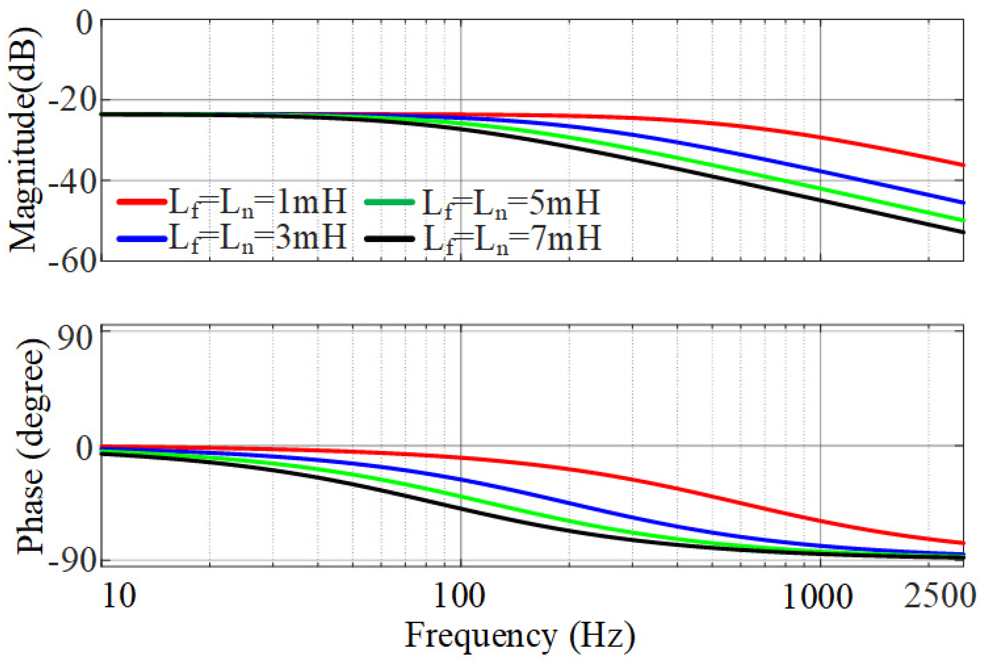
3.2. Zero-Sequence Impedance Characteristics of TFGI

From Equation (26), the zero-sequence admittance of TFGI can be expressed as,
Y z _ T F G I = 1 / ( s ( 3 L n + L f ) + 3 R n + R f + ( k 0 i p + k 0 i i s ) )
Figure 11 shows zero-sequence admittance bode diagrams of TFGI under different control bandwidths of the zero-axis current controller. Figure 11 shows that as the control bandwidth increases, the region with resistive characteristics gradually expands, and the admittance magnitude becomes smaller. Under the same bandwidth parameters, the zero-sequence admittance gradually changes from resistive characteristics to capacitive characteristics with the frequency increasing.
Figure 12 shows the zero-sequence admittance bode diagrams of TFGI when different filter parameters are applied. From Figure 12, the amplitude of the zero-sequence admittance of TFGI decreases and the region with resistive characteristic shrinks as the AC-side filter increases. Additionally, the zero-sequence admittance gradually transitions from resistive characteristics to capacitive characteristics as the frequency increases.

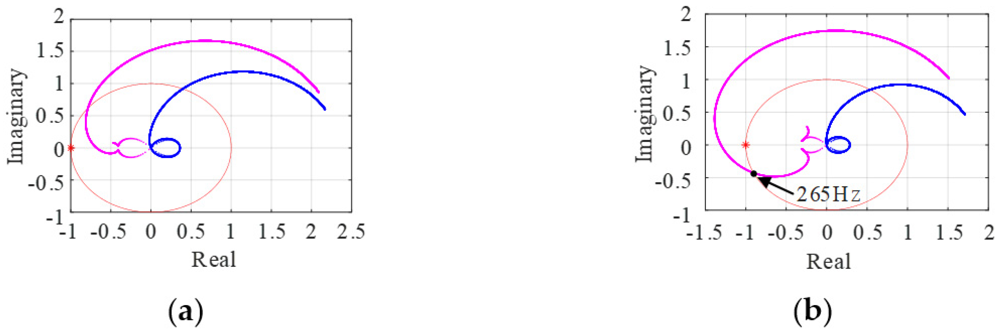
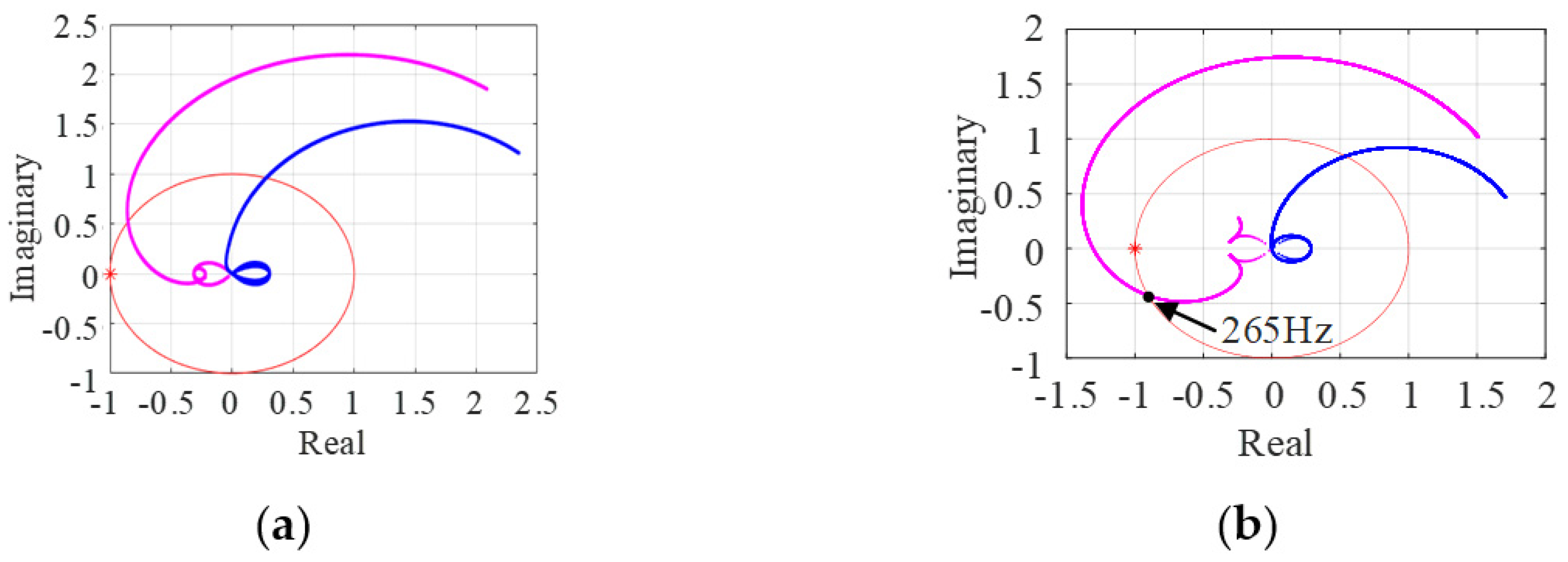
4. Stability Analysis

Based on the impedance stability theory [25], the small-signal stability of the three-phase four-wire grid-connected inverter system will be analyzed in this section. In order to investigate different impedance conditions of the distribution network and microgrid, the grid-side impedance can be intuitively equivalent to the circuit in Figure 13. In Figure 13, the capacitor Cg represents the parallel compensation degree, and the inductor Lg represents the strength of the grid. RCg and RLg present the parasitic resistance [10,11,12]. Hence, the grid impedance matrix can be expressed as,
Z g = [ Z g p 0 0 0 Z g n 0 0 0 Z g 0 ] = [ Z g p n 0 0 Z g 0 ]
where
Z g p = Z g n = ( s L g + R L g ) ( s C g R C g + 1 ) R C g ( s L g + R L g ) + s C g R C g + 1
Z g 0 = ( 1 + s C g R C g ) ( s ( L g + 3 L g n ) + R L g + 3 R L g n ) s C g ( s ( L a + 3 L g n ) + R L g + 3 R L g n ) + 1 + s C g R C g
To analyze the system stability, the generalized Nyquist criterion is applied to the Nyquist plot of the eigenvalues of Yipn0∗Zg, where the impedance ratio matrix can be written as,
L = Y i p n 0 Z g = [ Y i p n Z g p n 0 0 Y i 0 Z g 0 ]
From Equation (37), since the relationship between zero-sequence impedance and negative-sequence impedance as well as positive impedance is decoupled, the premise for the system to remain stable is that the positive and negative subsystems and the zero-sequence subsystem can remain stable at the same time. In other words, the system instability may be caused by positive- and negative-sequence components or may be brought about by the zero-sequence component.
Based on the above stability analysis theory, the adaptability and instability risk of TFSCI and TFGI in two typical grids, weak grids with and without parallel compensation, are studied in this section.

4.1. Weak Grid without Parallel Compensation

When the power grid is a weak grid without parallel compensation, the impedance of the grid can be expressed as shown in Equation (38). According to reference [26,27], the three-phase three-wire grid-connected inverter system has the instability risk caused by the SRF-PLL in the weak grid. Since the SRF-PLL also exists in the TFGI and TFSCI, along with the decoupled relationship between zero-sequence impedance and positive-sequence impedance as well as negative-sequence impedance, the three-phase four-wire inverter also has the instability risk caused by SRF-PLL. To avoid a repetitive discussion of similar content, a detailed analysis is not given in this paper. The figure below shows the root locus of Y i p n Z g p n when the proportional gain of SRF-PLL changes from 0.58 to 2.85. According to Figure 14, there is a risk of instability at 265 Hz.
Z g = [ Z g p 0 0 0 Z g n 0 0 0 Z g 0 ] = [ Z g p n 0 0 Z g 0 ]
where
Z g p n = [ s L g + R L g 0 0 s L g + R L g ]
Z g 0 = s ( L g + 3 L g n ) + R L g + 3 R L g n
Figure 15 shows the root locus of the inverter current when the phase currents ia, ib, and ic change from 0.5 p.u. to 1 p.u. According to Figure 14a, there is no risk of instability when ia = ib = ic = 0.5 p.u. According to Figure 14b, it also can be seen that there is a risk of instability at 265 Hz when ia = ib = ic =1 p.u.
In addition, the TFSCI also has the instability risk brought by the zero-sequence subsystem because, according to the bode diagram of the TFSCI shown in Figure 7, the impedance characteristics of the TFSCI undergo a gradual transition from capacitive characteristics to inductive characteristics. According to stability theory of impedance proposed in reference [25], in the frequency region where the zero-sequence impedance shows capacitive characteristics, if the phase angle difference of impedance between TFSCI and the weak grid at the impedance amplitude intersection is close to 180°, it will cause system small-signal instability. Figure 16 shows the zero-sequence admittance bode diagrams of TFSCI and grid when the risk of small-signal instability is caused by the zero-sequence component. In Figure 15, YSC33 is the zero-sequence admittance of the TFSCI and Yg0 is the zero-sequence admittances of grid.
According to the above analyses, the difference in zero-sequence impedance will lead to poor adaptability and a higher risk of instability of TFSCI compared with TFGI in the weak grid.

4.2. Weak Grid with Parallel Compensation

Under the weak grid with parallel compensation, the grid impedance can be expressed as Equation (34).
Combined with the bode diagram of the split capacitor inverter impedance, we know that there is a risk of high-frequency resonance in the system under the parallel compensation grid. The bode diagram of the capacitor split inverter impedance and grid impedance are shown in Figure 17. It can be seen from Figure 17 that the positive-sequence and negative-sequence impedances of the inverter are inductive at high frequency and the phase difference between the impedance of the TFSCI system and the impedance of the grid is 178°, close to 180°, at the amplitude intersection point 930 Hz. The zero-sequence impedance characteristics of the inverter gradually transition from capacitive to inductive and the phase difference between the impedance of TFSCI system and the impedance of the grid is 176°, close to 180°, at the amplitude intersection point 356 Hz. Figure 16 reveals that the system has a risk of resonance at 356 Hz and 930 Hz.
Similarly, combined with the bode diagram of the TFGI impedance, there is a risk of high-frequency resonance in the system. The bode diagram of the TFGI admittance and grid admittance are shown in Figure 18. According to Figure 18, the zero-sequence impedance, negative-sequence impedance, and positive-sequence impedance of TFGI are inductive at high frequency, and the phase difference between the impedance of TFSCI system and the impedance of grid is close to 180° at the amplitude intersection points 930 Hz and 460 Hz. Figure 18 reveals that the system has a risk of resonance at 930 Hz and 460 Hz.

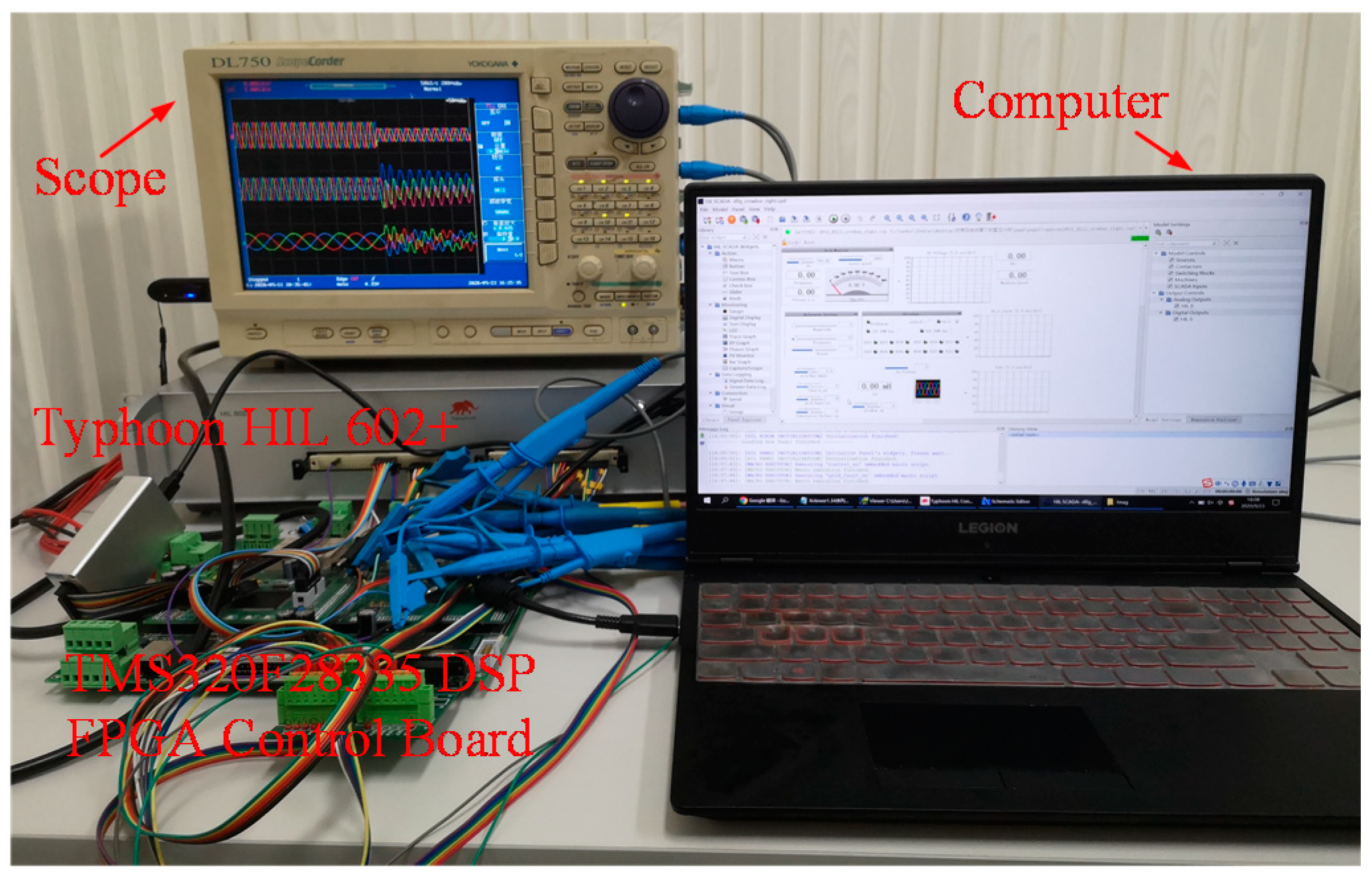
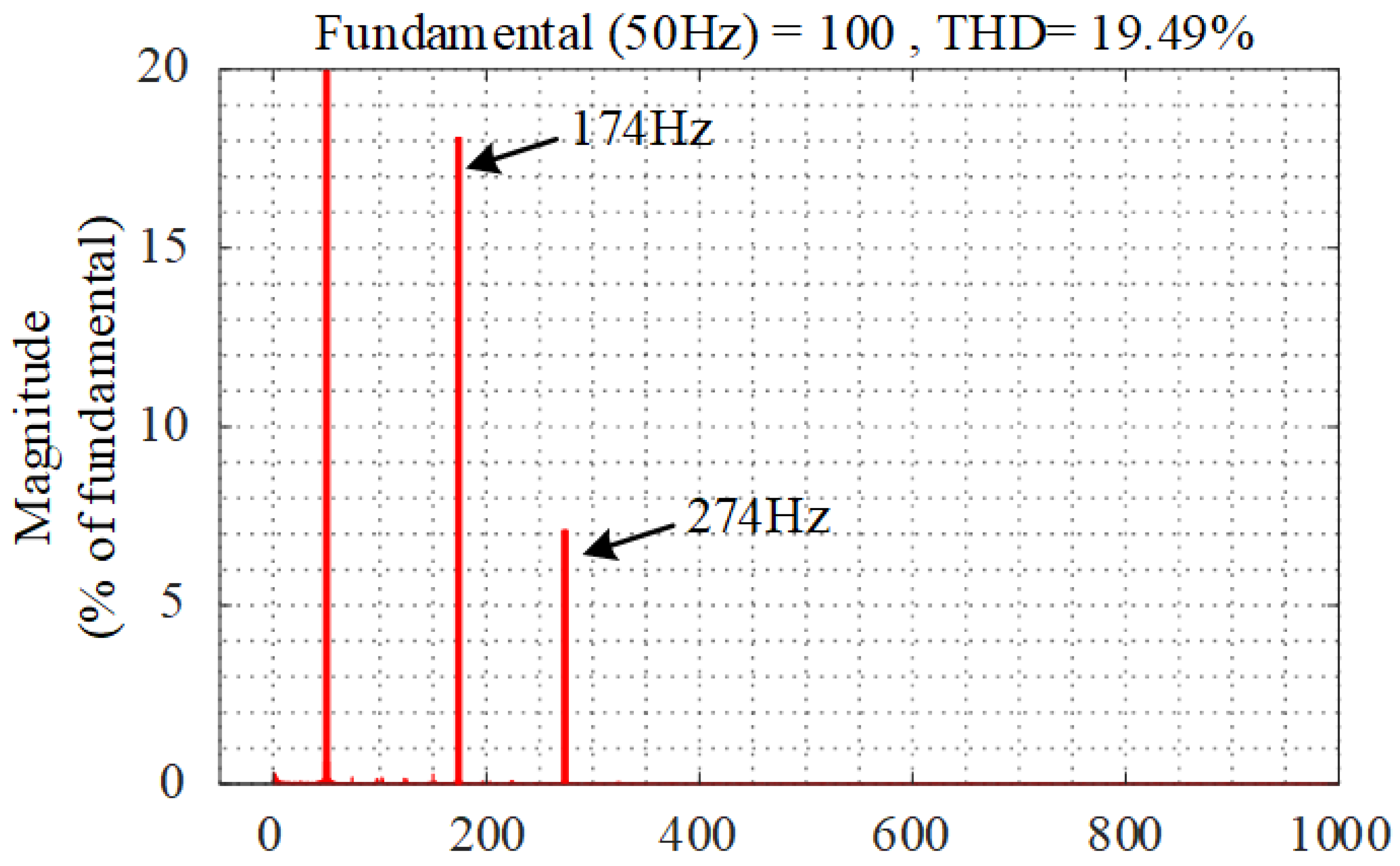
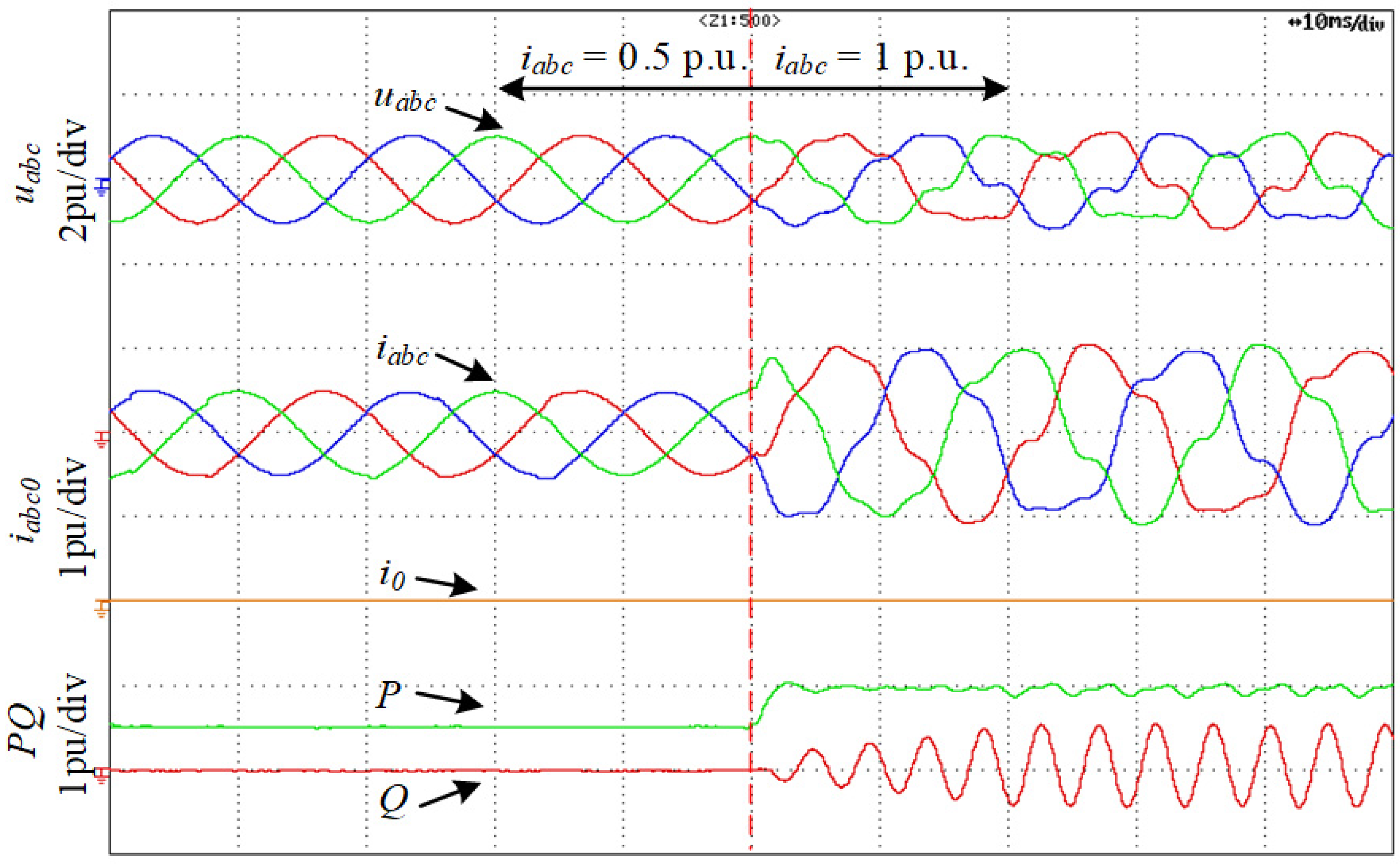
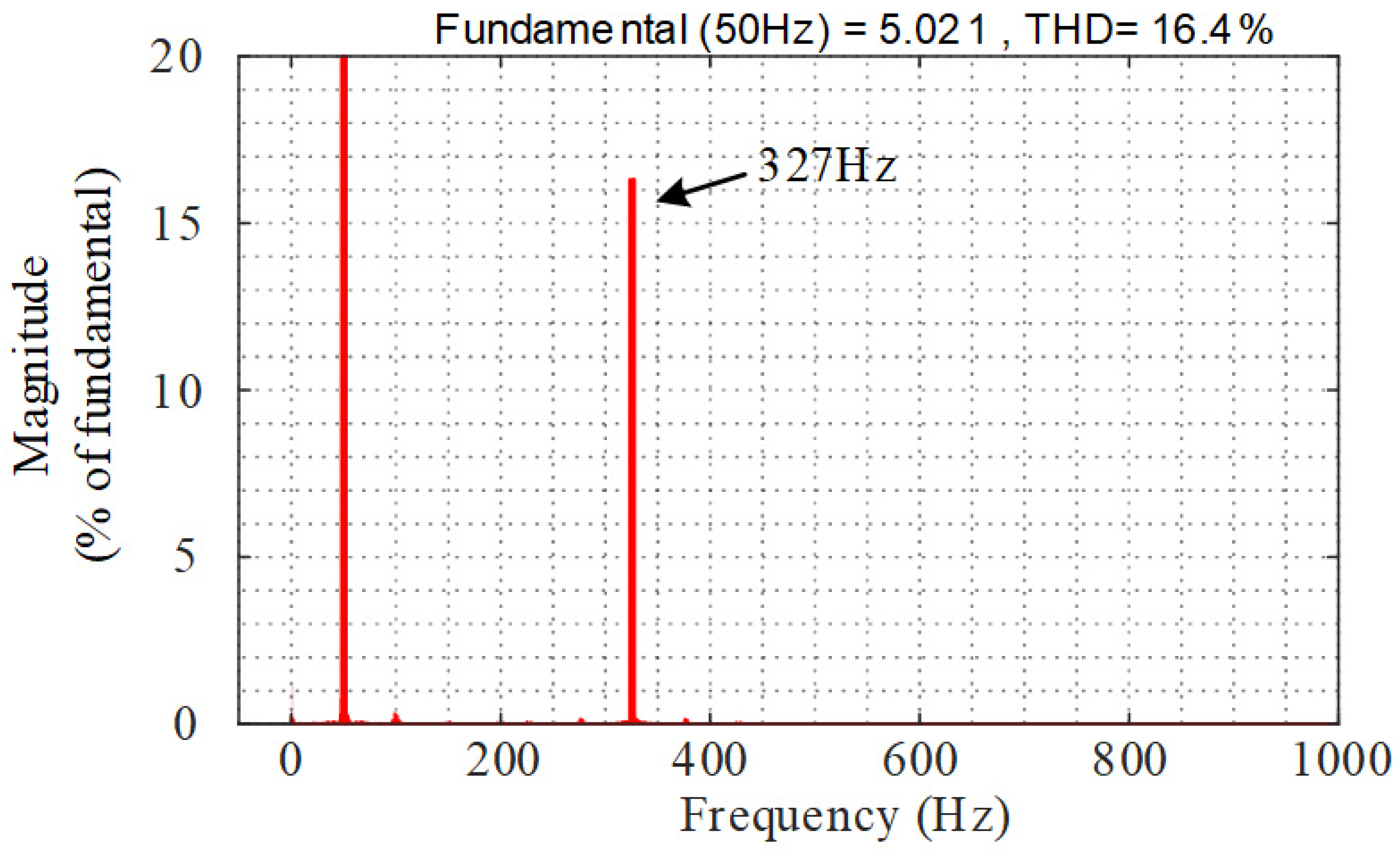
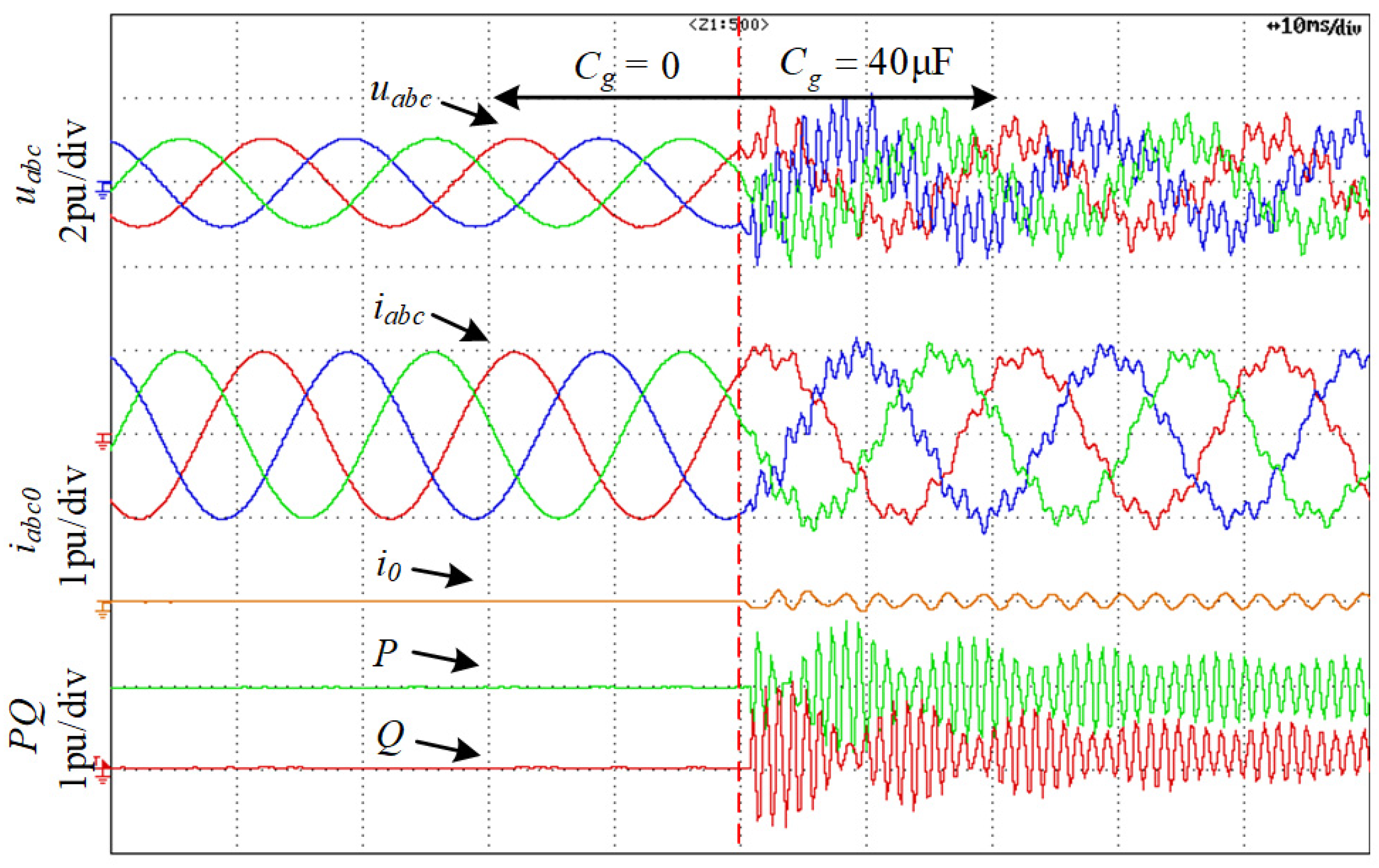
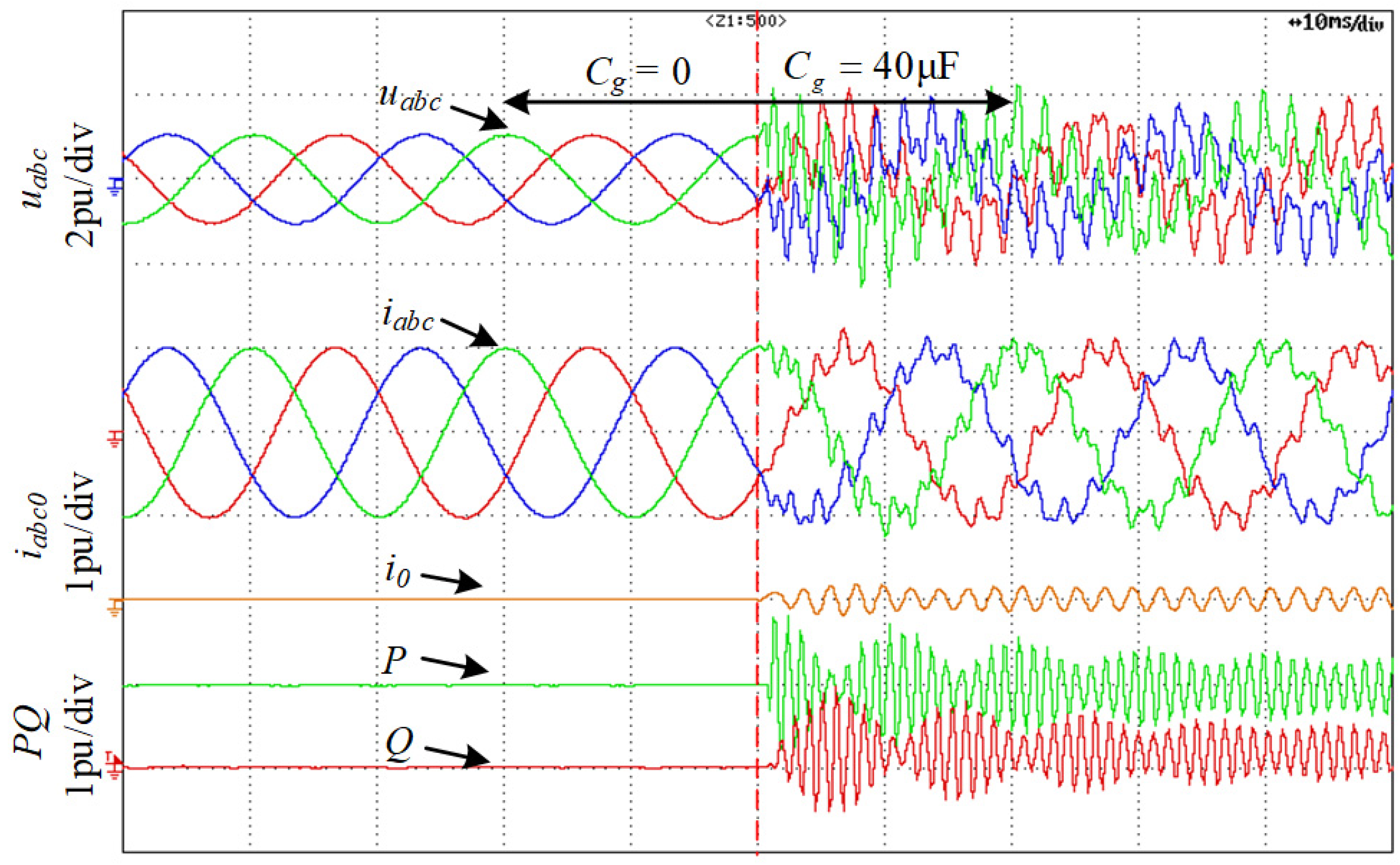
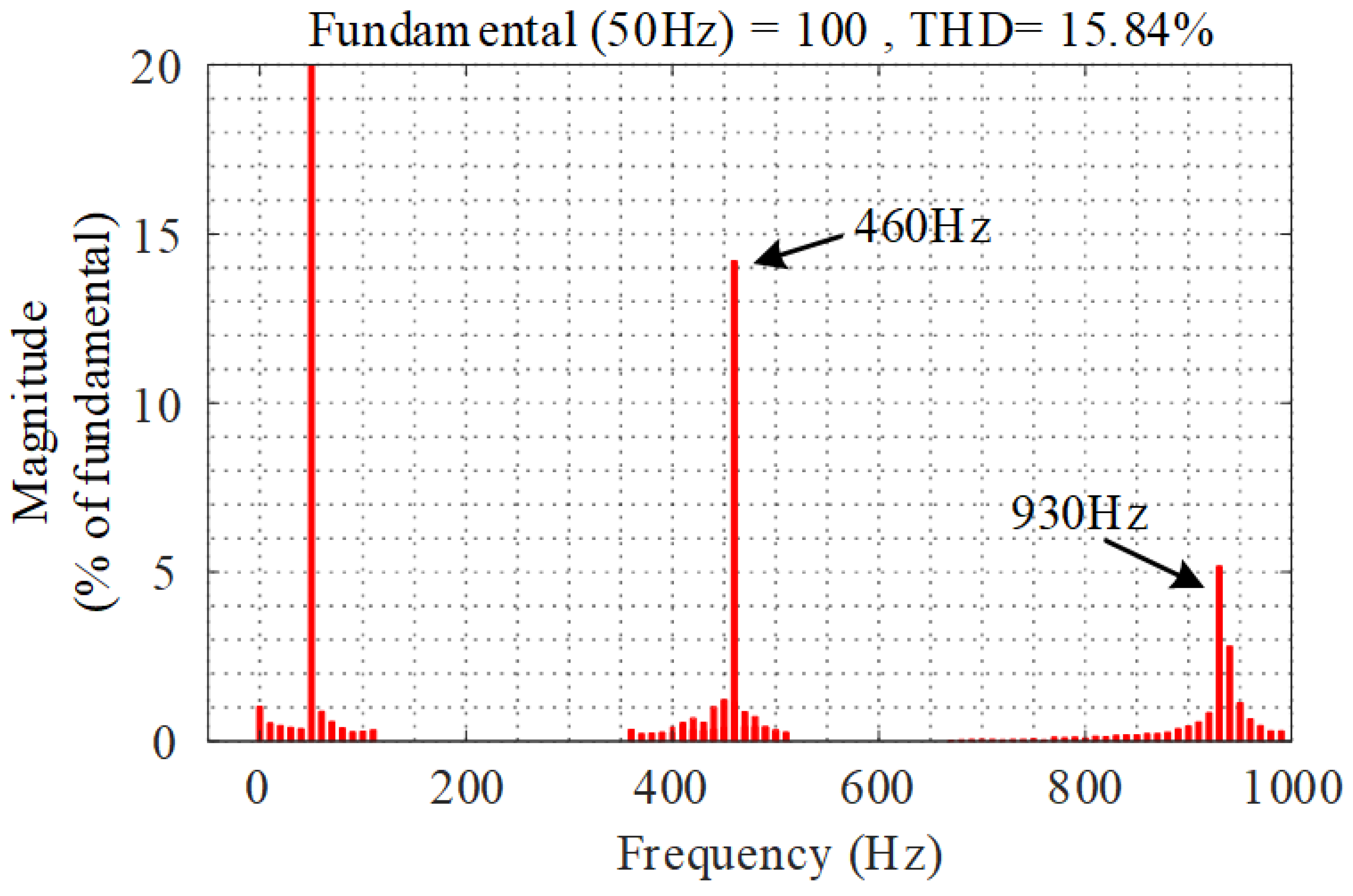
5. Experimental Verification

To better verify the achieved conclusions, the hardware platform based on control-hardware-in-loop (CHIL) is established, which can be seen in Figure 19. The models of the three-phase four-wire split capacitor grid-connected inverter system and the three-phase four-leg grid-connected inverter system are established in Typhoon 602 +. The controllers of TFSCI and TFGI are carried out on a TMS320F28335/Spartan6 XC6SLX16 DSP + FPGA control board. The CHIL was used to analyze and verify the conclusion presented in [28,29]. The corresponding parameters of the system are listed in Table A1 and Table A2 in Appendix C.
Figure 20 shows the voltages, currents, active power, and reactive power of the TFSCI when the SRF-PLL proportional gain (kpp) changes from 0.58 to 2.85. Figure 21 shows the FFT analysis of phase-a current (ia) when kpp = 2.85. It can be seen from Figure 20 and Figure 21 that there are considerable harmonic components at 174 Hz and 274 Hz in the system. From Figure 21, it also can be found that instability of the positive–negative-sequence sub-system occurs due to there being no zero-sequence harmonics in the system. The instability characteristics coincide with Figure 14.
Figure 22 shows the voltages, currents, active power, and reactive power of the TFSCI when the SRF-PLL proportional gain kpp = 2.85 and phase currents ia, ib, and ic change from 0.5 p.u. to 1 p.u. Figure 23 shows the FFT analysis of phase-a current (ia) when ia = ib = ic = 1 p.u. It can be seen from Figure 22 and Figure 23 that there are considerable harmonic components at 174 Hz and 274 Hz in the system. From Figure 22, it can also be found that instability of the positive- and negative-sequence sub-system occurs due to there being no zero-sequence harmonics in the system. The instability characteristics coincide with Figure 15.
Figure 24 shows the voltages, currents, active power, and reactive power of the TFSCI when the proportional gain of current PI controller (k0ip) changes from 3 to 10. Figure 25 shows the FFT analysis of phase-a current (ia) when k0ip = 10. It can be seen from Figure 24 and Figure 25 that there is a considerable harmonic component at 327 Hz in the system. From Figure 24, it also can be seen that instability of zero-sequence sub-system occurs. The instability characteristics coincide with Figure 16.
Figure 26 shows the voltages, currents, active power, and reactive power of the TFSCI connected to the parallel compensation grid when capacitor Cg changes from 0 to 40 μF. Figure 27 shows the FFT analysis of ia when Cg = 40 μF. It can be seen from Figure 26 and Figure 27 that there are considerable harmonic components at 365 Hz and 930 Hz in the system. From Figure 26, it also can be found that the resonance at 431 Hz is caused by the zero-sequence components and the resonance at 930 Hz is caused by the negative-sequence component and the positive-sequence component. The instability characteristics coincide with Figure 17.
Figure 28 shows the voltages, currents, active power, and reactive power of the TFGI connected to parallel compensation grid when capacitor Cg changes from 0 to 40 μF. Figure 29 shows the FFT analysis of phase-a current (ia) when Cg = 40 μF. It can be seen from Figure 28 and Figure 29 that there are considerable harmonic components at 460 Hz and 930 Hz in the system. From Figure 28, it also can be seen that the resonance at 431 Hz is generated by the zero-sequence component and the resonance at 930 Hz is brought about by the positive-sequence and negative-sequence components. The instability characteristics coincide with Figure 18.

6. Conclusions

The impedances of TFSCI and TFGI with consideration of the zero-sequence component were studied in this paper. The specific conclusions achieved here are as follows.
(1)
The impedance models of TFSCI and TFGI, commonly used in three-phase four-wire systems, including positive-sequence impedance, negative-sequence impedance, and zero-sequence impedance were established.
(2)
The similarity and difference of TFSCI impedance and TFGI impedance were revealed. The similarity lies in the similarity of the positive-sequence impedance and negative-sequence impedance. The difference is that the zero-sequence impedances are different, and these differences are mainly caused by the different zero-sequence current paths. The zero-sequence impedance of TFSCI has both capacitive and inductive characteristics, while the zero-sequence impedance of TFGI is mainly resistive and inductive.
(3)
The stability analysis was carried out through the impedance model, and the instability risk of the power grid under the weak grid and the parallel compensation grid were revealed. The difference in zero-sequence impedance leads to poor adaptability and higher instability risk of TFSCI compared with TFGI in the weak grid.
In addition, based on the established impedance of TFSCI and TFGI, the instability risk of the system can be analyzed through the impedance stability theory, and the phase margin can be improved when designing the system parameters to avoid system instability. When a small signal instability occurs in the system, the inverter impedance can be reshaped by changing the system parameters or the control strategy to restore the stability of the system.

Author Contributions

Conceptualization, Z.Y.; Investigation, Z.W.; Project administration, Y.X.; Validation, L.H.; Writing—original draft, G.F. All authors have read and agreed to the published version of the manuscript.

Funding

This research was funded by [the Naitional Natural Science Fundamentation of China] grant number [51507183, 51877212, 51807197].

Informed Consent Statement

This research article describing a study doesn’t involving humans.

Conflicts of Interest

The authors declare no conflict of interest.

Appendix A

According to Figure 3, the equation of the small-signal circuit model of TFSCI can be achieved as follows:
[ Δ u d s Δ u q s Δ u 0 s ] = [ L f 0 0 0 L f 0 0 0 L f + 3 L n ] [ p Δ i d s p Δ i q s p Δ i 0 s ] + [ R f 0 0 0 R f 0 0 0 R f + 3 R n ] [ Δ i d s Δ i q s Δ i 0 s ] + [ Δ d d s U d c Δ d q s U d c Δ u d c 2 U d c ] + [ D d s Δ u d c Δ D q s Δ u d c Δ D 0 s Δ u d c ]
In this paper, the DC voltage of the inverter is assumed to be constant to simplify the modeling process. Δ u d c = 0 .
Then,
[ Δ u d s Δ u q s Δ u 0 s ] = [ L f 0 0 0 L f 0 0 0 L f + 3 L n ] [ p Δ i d s p Δ i q s p Δ i 0 s ] + [ R f 0 0 0 R f 0 0 0 R f + 3 R n ] [ Δ i d s Δ i q s Δ i 0 s ] + [ Δ d d s U d c Δ d q s U d c Δ u d c 2 + Δ d 0 s U d c ]
According to the Laplace transformation, the following equation can be achieved:
[ Δ u d s Δ u q s Δ u 0 s ] = [ s L f + R f ω L f 0 ω L f s L f + R f 0 0 0 s ( L f + 3 L n ) + R f + 3 R n ] [ Δ i d s Δ i q s Δ i 0 s ] + [ Δ d d s U d c Δ d q s U d c Δ u d c 2 + Δ d 0 s U d c ]
Assuming Δ d d s = Δ d q s = Δ d 0 s , the relationship between the small-signal perturbation voltage and the corresponding current in the system frame can be expressed as:
[ Δ u d s Δ u q s Δ u 0 s ] = [ s L f + R f ω L f 0 ω L f s L f + R f 0 0 0 s ( L f + 3 L n ) + R f + 3 R n ] [ Δ i d s Δ i q s Δ i 0 s ] + [ 0 0 Δ u d c 2 ]
Combining Equation (4), the transfer function matrix from perturbation voltage to current response in the system frame can be expressed as follows.
Z S C o u t = [ s L f + R f ω L f 0 ω L f s L f + R f 0 0 0 s ( L f + 3 L n ) + R f + 3 R n 3 2 s C ]

Appendix B

Figure A1 shows the bode diagrams of the analytical admittance and frequency scanning admittance of the TFSCI and TFGI, in which Yij denotes the ith element in the jth column in the admittance matrix of TFSCI Y SCpn 0 and the admittance matrix of TFGI Y FLpn 0 .
Figure A1. Bode diagram comparation of the output admittance of the inverter (red curve denotes the established model result and blue asterisk denotes the frequency scanning measurement result).
Energies 15 02754 g0a1aEnergies 15 02754 g0a1b

Appendix C

Table A1. Three-phase four-wire split capacitor inverter parameters.
SymbolParameterValue
UsRated voltage380 V
PnRated power 30 kW
f1Fundamental frequency50 Hz
fsSwitching frequency5 kHz
LfFilter inductance3 mH
RLfParasitic resistance of filter inductance0.02 Ω
kppSRF-PLL proportional gain 0.58
kpiSRF-PLL integral gain0.25
kdipd-axis current controller proportional gain1
kdiid-axis current controller integral gain18
kqipq-axis current controller proportional gain1
kqiiq-axis current controller integral gain18
k0ip0-axis current controller proportional gain3
k0ii0-axis current controller integral gain54
kdcpProportional parameter of DC voltage balance PI controller2.1
kdciIntegral parameter of DC voltage balance PI controller4.2
Table A2. Three-phase four-leg inverter parameters.
SymbolParameterValue
UsRated voltage380 V
PnRated power 30 kW
f1Fundamental frequency50 Hz
fsSwitching frequency5 kHz
LfFilter inductance3 mH
RLfParasitic resistance of filter inductance0.02 Ω
kppSRF-PLL proportional gain0.58
kpiSRF-PLL integral gain0.25
kdipd-axis current controller proportional gain1
kdiid-axis current controller integral gain18
kqipq-axis current controller proportional gain1
kqiiq-axis current controller integral gain 18
k0ip0-axis current controller proportional gain3
k0ii0-axis current controller integral gain 54
Table A3. List of some special symbols.
SymbolParameter
pDifferential operator
sLaplace operator
XcVariable in the controller dq0 frame
XsVariable in the system dq0 frame
dDuty ratio

References

  1. Primadianto, A.; Lu, C.-N. A Review on Distribution System State Estimation. IEEE Trans. Power Syst. 2017, 32, 3875–3883. [Google Scholar] [CrossRef]
  2. Ahmad, F.; Rasool, A.; Ozsoy, E.; Sekar, R.; Sabanovic, A.; Elitaş, M. Distribution system state estimation—A step towards smart grid. Renew. Sustain. Energy Rev. 2018, 81, 2659–2671. [Google Scholar] [CrossRef] [Green Version]
  3. Cavraro, G.; Arghandeh, R. Power distribution network topology detection with time-series signature verification method. IEEE Trans. Power Syst. 2018, 33, 3500–3509. [Google Scholar] [CrossRef]
  4. Zhou, X.; Tang, F.; Loh, P.C.; Jin, X.; Cao, W. Four-Leg Converters with Improved Common Current Sharing and Selective Voltage-Quality Enhancement for Islanded Microgrids. IEEE Trans. Power Deliv. 2016, 31, 522–531. [Google Scholar] [CrossRef] [Green Version]
  5. Hirve, S.; Chatterjee, K.; Fernandes, B.G.; Imayavaramban, M.; Dwari, S. PLL-Less Active Power Filter Based on One-Cycle Control for Compensating Unbalanced Loads in Three-Phase Four-Wire System. IEEE Trans. Power Deliv. 2007, 22, 2457–2465. [Google Scholar] [CrossRef] [Green Version]
  6. Morais, A.; Tofoli, F.L.; Barbi, I. Modeling, Digital Control, and Implementation of a Three-Phase Four-Wire Power Converter Used as A Power Redistribution Device. IEEE Trans. Ind. Inf. 2016, 12, 1035–1042. [Google Scholar] [CrossRef]
  7. Kerekes, T.; Teodorescu, R.; Liserre, M.; Klumpner, C.; Sumner, M. Evaluation of Three-Phase Transformerless Photovoltaic Inverter Topologies. IEEE Trans. Power Electron. 2009, 24, 2202–2211. [Google Scholar] [CrossRef]
  8. Pichan, M.; Rastegar, H. Sliding-Mode Control of Four-Leg Inverter with Fixed Switching Frequency for Uninterruptible Power Supply Applications. IEEE Trans. Ind. Electron. 2018, 64, 6805–6814. [Google Scholar] [CrossRef]
  9. Carlos, G.; Jacobina, C.B.; Santos, E. Investigation on Dynamic Voltage Restorers with Two DC Links and Series Converters for Three-Phase Four-Wire Systems. IEEE Trans. Ind. Appl. 2016, 52, 1608–1620. [Google Scholar] [CrossRef]
  10. Shukla, A.; Ghosh, A.; Joshi, A. Hysteresis current control operation of flying capacitor multilevel inverter and its application in shunt compensation of distribution systems. IEEE Trans. Power Deliv 2007, 22, 396–405. [Google Scholar] [CrossRef] [Green Version]
  11. Ramos-Carranza, H.A.; Medina, A.; Chang, G.W. Real-Time Shunt Active Power Filter Compensation. IEEE Trans. Power Deliv. 2008, 23, 2623–2625. [Google Scholar] [CrossRef]
  12. Wandhare, R.G.; Agarwal, V. Reactive power capacity enhancement of a PV-grid system to increase PV penetration level in smart grid scenario. IEEE Trans. Smart Grid. 2014, 5, 1845–1854. [Google Scholar] [CrossRef]
  13. Middlebrook, R.D. Measurement of loop gain in feedback systems. Int. J. Electron. 1975, 38, 485–512. [Google Scholar] [CrossRef]
  14. Panov, Y.; Jovanovic, M.M. Stability and dynamic performance of current-sharing control for paralleled voltage regulator modules. IEEE Trans. Power Electron. 2002, 17, 172–179. [Google Scholar] [CrossRef] [Green Version]
  15. Morroni, J.; Zane, R.; Maksimovic, D. An Online Stability Margin Monitor for Digitally Controlled Switched-Mode Power Supplies. IEEE Trans. Power Electron. 2009, 24, 2639–2648. [Google Scholar] [CrossRef] [Green Version]
  16. Bottrell, N.; Prodanovic, M.; Green, T.C. Dynamic Stability of a Microgrid with an Active Load. IEEE Trans. Power Electron. 2013, 28, 5107–5119. [Google Scholar] [CrossRef] [Green Version]
  17. Zeng, J.; Zhe, Z.; Qiao, W. An interconnection and damping assignment passivity-based controller for a DC–DC boost converter with a constant power load. IEEE Trans. Ind. Appl. 2014, 50, 2314–2322. [Google Scholar] [CrossRef]
  18. Gu, Y.; Li, W.; He, X. Passivity-Based Control of DC Microgrid for Self-Disciplined Stabilization. IEEE Trans. Power Syst. 2015, 30, 2623–2632. [Google Scholar] [CrossRef]
  19. Middlebrook, R.D. Input filter considerations in design and application of switching regulators. In Proceedings of the IEEE Industry Applications Society Annual Meeting, Chicago, IL, USA, 11–14 October 1976; pp. 94–107. [Google Scholar]
  20. Sun, J. Small-signal methods for ac distributed power systems-A review. IEEE Trans. Power Electron. 2009, 24, 2545–2554. [Google Scholar]
  21. Ren, Y.; Wang, X.; Chen, L.; Min, Y.; Li, G.; Wang, L.; Zhang, Y. A Strictly Sufficient Stability Criterion for Grid-Connected Converters Based on Impedance Models and Gershgorin’s Theorem. IEEE Trans. Power Deliv. 2020, 35, 1606–1609. [Google Scholar] [CrossRef]
  22. Song, S.; Guan, P.; Liu, B.; Lu, Y.; Goh, H. Impedance Modeling and Stability Analysis of DFIG-Based Wind Energy Conversion System Considering Frequency Coupling. Energies 2021, 14, 3243. [Google Scholar] [CrossRef]
  23. Xu, Y.; Nian, H.; Wang, Y.; Sun, D. Impedance Modeling and Stability Analysis of VSG Controlled Grid-Connected Converters with Cascaded Inner Control Loop. Energies 2020, 13, 5114. [Google Scholar] [CrossRef]
  24. Cespedes, M.; Sun, J. Impedance Modeling and Analysis of Grid-Connected Voltage-Source Converters. IEEE Trans. Power Electron. 2014, 29, 1254–1261. [Google Scholar] [CrossRef]
  25. Sun, J. Impedance-Based Stability Criterion for Grid-Connected Inverters. IEEE Trans. Power Electron. 2011, 26, 3075–3078. [Google Scholar] [CrossRef]
  26. Rygg, A.; Molinas, M.; Zhang, C.; Cai, X. A Modified Sequence-Domain Impedance Definition and Its Equivalence to the dq-Domain Impedance Definition for the Stability Analysis of AC Power Electronic Systems. IEEE J. Emerg. Sel. Top. Power Electron. 2016, 4, 1383–1396. [Google Scholar] [CrossRef] [Green Version]
  27. Nian, H.; Liao, Y.; Li, M.; Sun, D.; Xu, Y.; Hu, B. Impedance Modeling and Stability Analysis of Three-Phase Four-Leg Grid-Connected Inverter Considering Zero-Sequence. IEEE Access 2021, 9, 83676–83687. [Google Scholar] [CrossRef]
  28. Hu, B.; Nian, H.; Yang, J.; Li, M.; Xu, Y. High-Frequency Resonance Analysis and Reshaping Control Strategy of DFIG System Based on DPC. IEEE Trans. Power Electron. 2021, 36, 7810–7819. [Google Scholar] [CrossRef]
  29. Nian, H.; Yang, J.; Hu, B.; Jiao, Y.; Xu, Y.; Li, M. Stability Analysis and Impedance Reshaping Method for DC Resonance in VSCs-based Power System. IEEE Trans. Energy Convers. 2021, 36, 3344–3354. [Google Scholar] [CrossRef]
Figure 1. Block diagram of TFSCI.
Energies 15 02754 g001
Figure 2. Block diagram of PLL.
Energies 15 02754 g002
Figure 3. Small-signal circuit model of TFSCI. (a) Small-signal circuit in d-axis; (b) small-signal circuit in q-axis; (c) small-signal circuit in 0-axis.
Energies 15 02754 g003
Figure 4. Relationship between controller frame and system frame.
Energies 15 02754 g004
Figure 5. The impedance model block diagram of TFSCI.
Energies 15 02754 g005
Figure 6. Block diagram of TFGI.
Energies 15 02754 g006
Figure 7. The zero_sequence admittance bode diagrams of TFSCI under different filter parameters.
Energies 15 02754 g007
Figure 8. The zero_sequence admittance bode diagrams of TFSCI under different control bandwidths of zero-axis current controller.
Energies 15 02754 g008
Figure 9. The zero_sequence admittance bode diagrams of TFSCI under different DC_side capacitors Cdc.
Energies 15 02754 g009
Figure 10. The zero_sequence admittance bode diagrams of TFSCI under different bandwidths of DC_voltage balance PI controller.
Energies 15 02754 g010
Figure 11. The zero_sequence admittance bode diagrams of TFSCI under different control bandwidths of zero_axis current controller.
Energies 15 02754 g011
Figure 12. The zero_sequence admittance bode diagrams of TFGI under different filter parameters.
Energies 15 02754 g012
Figure 13. The equivalent circuit of the grid impedance.
Energies 15 02754 g013
Figure 14. Characteristic root locus of Yipn·Zgpn. (a) Proportional gain of SRF-PLL kpp = 0.58. (b) Proportional gain of SRF_PLL kpp = 2.85.
Energies 15 02754 g014
Figure 15. Characteristic root locus of Yipn·Zgpn. (a) Proportional gain of SRF_PLL kpp = 2.85 and phase current ia = ib = ic = 0.5 p.u. (b) Proportional gain of SRF_PLL kpp = 2.85 and phase currents ia = ib = ic = 1 p.u.
Energies 15 02754 g015
Figure 16. The zero_sequence admittance bode diagrams of TFSCI and grid when the small_signal instability is caused by the zero_sequence component.
Energies 15 02754 g016
Figure 17. Admittance model of TFSCI and the grid, when the small_signal instability is caused by zero-sequence component, positive_sequence component, and negative-sequence components.
Energies 15 02754 g017
Figure 18. Admittance model of TFGI and the grid, when the small-_signal instability is caused by zero_sequence, positive-sequence, and negative_sequence components.
Energies 15 02754 g018
Figure 19. Hardware platform of CHIL experiment.
Energies 15 02754 g019
Figure 20. Experiment results of the instability of positive–negative-sequence sub-system when kpp changes from 0.58 to 2.85.
Energies 15 02754 g020
Figure 21. FFT analysis of ia when kpp = 2.85.
Energies 15 02754 g021
Figure 22. Experiment results of the instability of positive–negative-sequence sub-system when kpp changes from 0.58 to 2.85.
Energies 15 02754 g022
Figure 23. FFT analysis of ia when ia = ib = ic = 1 p.u.
Energies 15 02754 g023
Figure 24. Experiment results of the instability of zero-sequence sub-system when k0ip changes from 3 to 10.
Energies 15 02754 g024
Figure 25. FFT analysis of ia when k0ip = 10.
Energies 15 02754 g025
Figure 26. Experiment results of the instability of TFSCI when Cg changes from 0 to 40 μF.
Energies 15 02754 g026
Figure 27. FFT analysis of ia of TFSCI when Cg = 40 μF.
Energies 15 02754 g027
Figure 28. Experiment result of the instability of TFGI when Cg changes from 0 to 40 μF.
Energies 15 02754 g028
Figure 29. FFT analysis of ia f of TFGI when Cg = 40 μF.
Energies 15 02754 g029
Publisher’s Note: MDPI stays neutral with regard to jurisdictional claims in published maps and institutional affiliations.

