Article

Design and Real-Time Implementation of a Control System for SiC Off-Board Chargers of Battery Electric Buses

1
MOBI-EPOWERS Research Group, ETEC Department, Vrije Universiteit Brussel (VUB), Pleinlaan 2, 1050 Brussel, Belgium
2
Flanders Make, Gaston Geenslaan 8, 3001 Heverlee, Belgium
*
Author to whom correspondence should be addressed.
Energies 2022, 15(4), 1434; https://doi.org/10.3390/en15041434
Submission received: 26 December 2021 / Revised: 11 February 2022 / Accepted: 13 February 2022 / Published: 16 February 2022
(This article belongs to the Special Issue The Future Development of Automobile Energy)

Abstract

:
Emerging wide bandgap (WBG) semiconductors, such as silicon carbide (SiC), will enable chargers to operate at higher switching frequencies, which grants the ability to deliver high power and enhances efficiency. This paper addresses the modeling of a double-sided cooling (DSC) SiC technology-based off-board charger for battery electric buses (BEBs) and the design of its control and real-time (RT) implementation. A three-phase active front-end (AFE) rectifier topology is considered in the modeling and control system design for the active part of the DC off-board charger. The control system consists of a dual-loop voltage–current controller and is used to ensure AC to DC power conversion for charging and to achieve the targeted grid current total harmonic distortion (THD) and unity power factor (PF). Linear and nonlinear simulation models are developed in MATLAB/Simulink for optimum control design and to validate the voltage and current control performances. Four types of controllers (i.e., proportional–integral (PI), lead–lag, proportional–resonant (PR), and modified proportional–resonant (MPR)) are designed as current controllers, and a comparative analysis is conducted on the simulation model. In addition, the final design of the dual-loop controller is implemented on the RT–FPGA platform of dSpace MicroLabBox. It is then tested with the charger to validate the control performance with experimental data. The simulation and experimental results demonstrate the correct operation of the converter control performance by tracking the reference commands.

Graphical Abstract

1. Introduction

The share of battery electric buses (BEBs) used in public transportation is steadily increasing every year, as BEBs are beneficial in our battle against global warming, considering the electric energy comes from a clean energy mix. However, an appropriate off-board charging infrastructure is required to charge BEBs in an efficient way. Such chargers are intended to have high power ratings and fast charging speeds, and are less limited by size or weight [1]. They consist of power electronic converters (PECs), which transform three-phase incoming AC grid power into a variable DC output power to charge the battery of the BEB. PECs are designed to protect the power quality of the grid through the consumption of a sinusoidal current, which reduces the THD of the line current with PF control in order to comply with international standards, such as IEC-1000-3-2 and IEEE-519 [2]. They are also designed to charge batteries with variable voltages and current levels while keeping the batteries safe [3].
Recently, advanced WBG materials (SiC and GaN) have been introduced into the switching technology of PECs [4,5]. Semiconductor materials based on WBG technology offer interesting features over traditional Si materials, as shown in Figure 1. These include high voltage operation and a low leakage current, high-frequency operation, high thermal conductivity, high electron saturation speed, and high electron mobility. Traditional Si semiconductor-based PECs are commercially available. Studies show that WBG-based semiconductor technology has advantages over standard Si devices. SiC reduces power losses by 25% and volume by 50% by operating at a high frequency [6,7]. Accordingly, SiC-based semiconductors are very suited for BEBs’ DC charger applications due to their high switching frequency, high voltage, high power, and high-temperature operation. However, state-of-the-art research is needed to integrate WBG-based devices into existing and new applications. Indeed, there is a lack of accurate models of such systems and new controllers to cope with the devices’ high switching frequencies and fast dynamics. Moreover, the commercially available off-board chargers for BEBs mostly have an efficiency >95% [8]. This research aims to design a charger for the specification of BEBs to enhance efficiency >97% and reduce size and weight through the integration of WBG semiconductors.
Numerous control techniques have been discussed in the literature to prevent high energy transfer damage at high power [9]. Most control procedures were established for grid-side AFE converter applications. They are based on direct active and reactive power control [10]. The conventional technique of battery chargers is known as constant current–constant voltage (CC–CV). The basic premise of this technique is that the battery is charged to a certain voltage with a maximum constant current according to cell capacity and then charged at a constant voltage until the drawn current decreases to C/10 or less, where C states the charge or discharge rate of the battery over one hour. The CC–CV control helps to speed up the battery charging time. Thus, a standard dual-loop control strategy is proposed for the application of high power and high voltage DC off-board chargers of BEBs. The controller controls the DC battery voltage and current through active–reactive power control. The new vision of this study is to integrate the WBG SiC semiconductor and appropriate control approach for the emerging application of BEBs off-board chargers. Another study is needed to determine which controller, such as PI, Lead-League, PR, or MPRC, is relevant for the high-frequency dynamics of SiC devices and the high-power DC chargers of BEBs. The outer loop controls the battery parameters, and the inner loop controls the grid powers and quality [10]. The inner loop control bandwidth is chosen based on the operating frequency of the switching device to achieve the desired response [11,12].
Research shows that the control design and implementation of accurate real-time controllers is another challenge for PECs. Conventionally, digital embedded controllers such as microprocessors, microcontrollers, and digital signal processors (DSPs) have been used to implement pulse-width modulation (PWM) algorithms for PECs. However, techniques based on these controllers have the disadvantages of limited functionality and low computational speed for complex PWM circuits [13]. Xilinx has developed a programmable logic tool called Field-Programmable Gate Array (FPGA) [14]. It can be applied to real-time hardware-in-the-loop (HIL) implementation due to its performance, computing capacity, and ability to perform parallel data processing [14]. An FPGA consists of thousands of logic gates grouped together as configurable logic blocks to facilitate high-level circuit design [15]. They are preferred for prototyping application-specific integrated circuits (ASICs) because of their configuration and program capabilities [13].
FPGAs provide significant opportunities for power electronic applications and real-time hardware emulation. Currently, FPGAs appear as an alternative to the digital control of high-frequency PWM converters over DSPs and DSCs. Rapid control prototyping (RCP) platforms based on FPGAs, such as dSPACE and Opal-RT, are new technologies for designing and validating controllers in model-in-the-loop (MIL) simulations without actually implementing them in hardware systems [16]. Such platforms can be used for reconfigurability, co-simulation, HIL, automated Verilog hardware description language (VHDL) code generation, and system scalability, and enable embedded design engineers to quickly build state-of-the-art digital control algorithms while reducing design and testing time [17,18,19]. Therefore, RCP–FPGA is probably the most suitable tool for implementing all the digital functions of WBG-based power converters. It highlights the potential of such devices as it demonstrates the need for high-frequency control and modulation [20,21].
This research is also dedicated to implementing real-time controls in the FPGA platform so that WBG devices can be integrated into state-of-the-art applications to operate at higher frequencies beyond the limits of the conventional DSP.
The DSC SiC MOSFET based on advanced technology is used for charger development. A new double-sided liquid cooling concept has been applied to cool the charger’s DSC modules at a high power. The control strategy is designed for the SiC off-board charger to charge the batteries in different operational modes with voltage and current control. The controller is designed using the analytical model according to the passive filters of the converter, then tested in simulation at rated power. Disturbance rejection analyses are performed in simulations before implementing real time (RT) to determine which controller is suitable for this application. Four types of controllers, namely the PI, lead–lag, PR, and MPR controllers, are analyzed in simulation. The discrete FPGA-based controller is implemented on RT dSpace microlabbox using Xilinx Vivado. Finally, a test is performed on an experimental setup based on DSC SiC modules at 40 kHz. It demonstrates the behaviour of an off-board charger with compact DSC SiC switches to contribute to all studies dedicated to WBG semiconductors in Electrical Vehicle (EV) applications. The results can be used to develop compact and highly efficient EV converters. The FPGA-based implemented controller can also generate PWM signals at higher switching frequencies such as 100 kHz and 200 kHz.
This paper is arranged into different sections. Section 2 of this paper describes the system architecture. Section 3 clearly illustrates the linear modeling and control design optimization. In Section 4, the results of the dynamic simulation model are explained. Section 5 is dedicated to the real-time implementation of the controller in FPGA/Xilinx of dSpace MicrolabBox, whereas Section 6 describes the experimental setup and experimental results. Finally, the conclusions are provided in Section 7.

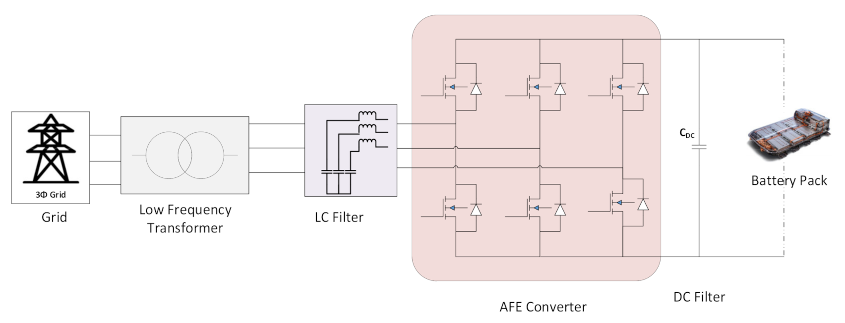
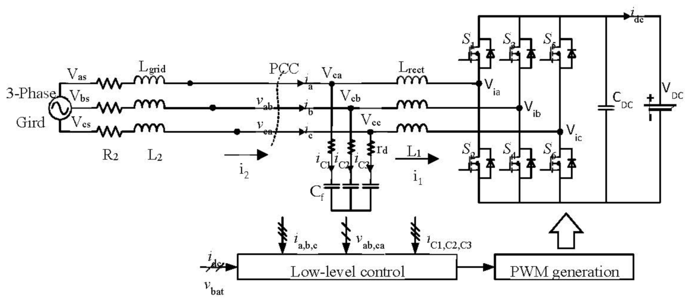
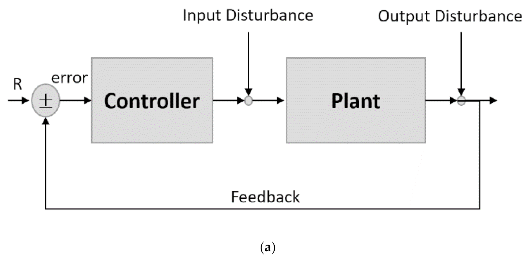
2. System Architecture

The three-phase AFE converter was selected in this study, since it is often employed in high-power applications. As shown in Figure 2, the architecture comprises of a low frequency (LF) isolation transformer, an inductor–capacitor (LC) filter, and a SiC-based AC/DC converter operating at a 40 kHz switching frequency [14], which converts three-phase incoming AC power into a variable DC output power. For the controller design and to get the best potential outcomes in terms of performance, efficiency, and power losses, accurate modelling of this AFE converter is essential [5,22].

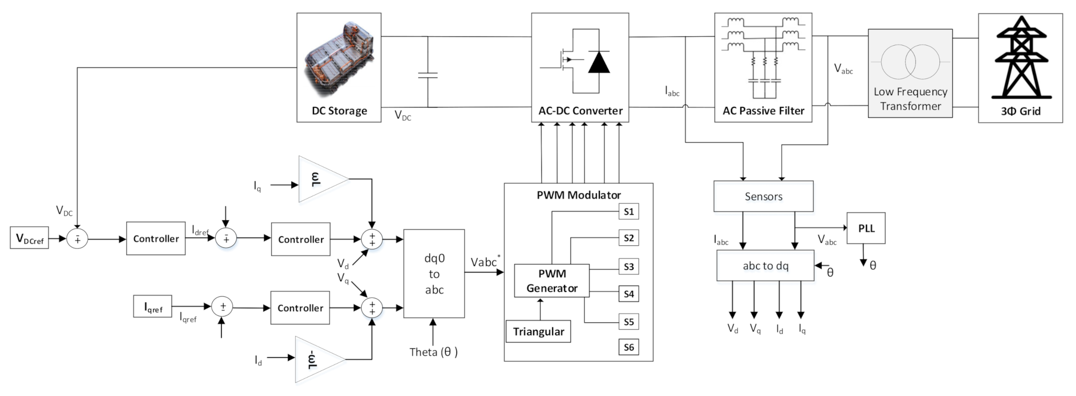
3. System Modeling and Control Design

3.1. Linear Modeling

Deriving the mathematical or linear model of a system is a long process. Models are necessary for understanding the system’s dynamics and for verifying compliance with the system’s requirements. In the form of state space, a linear model was built based on the generalized system model. This linear model was used for offline control design and stability and controllability analysis. In dq0 frames of reference, the linear model of the AFE converter (as depicted in Figure 3) was generated [7,22].
The high rated power of the AC–DC converter needed to guarantee a high PF on the AC grid and an appropriate total harmonic distortion (THD) for the grid line currents.
The off-board charger’s specifications and AC and DC passive filters are illustrated in Table 1.
An analytical-based model was created for the off-board charger of the AC–DC converter. Equations (1)–(7) were derived in a dq0- frame of reference for the AFE three-phase converter, also based on Figure 3 [22]. The differential first-order equations with LCL filter and DC filter were used to create the state space linear model [11,12].
V ds = R l 2 i 2 ds + R d i 2 ds + L 2 di 2 ds dt ω L 2 i 2 qs + V cd R d i 1 ds
V qs = R l 2 i 2 qs + R d i 2 qs + L 2 di 2 qs dt + ω L 2 i 2 ds + V cq R d i 1 qs
0 = i 2 ds + C f dV cd dt ω C f V cq + i 1 ds
0 = i 2 qs + C f dV cd dt + ω C f V cd + i 1 qs
V ids = R l 1 i 1 ds + R d i 2 ds + L 1 di 1 ds dt ω L 1 i 1 qs V cd R d i 2 ds
V iqs = R l 1 i 1 qs + R d i 1 qs + L 1 di 1 qs dt + ω L 1 i 1 ds + V cq R d i 2 qs
C DC dV dc dt = 3 2 M d i 1 ds + 3 2 M q i 1 qs V dc R
where V ds ,   V qs ,   V 0 s [V] are the grid AC voltages; i 2 ds ,   i 2 qs , i 1 ds ,   i 1 qs [A] are the AC currents of the grid and inductor side, respectively, in the dq0 frame; V DC [V] is DC voltage, V id ,   V iq [V] are converter voltages; [V] are voltages across the AC capacitor; and M d ,   M q are modulation indices in the dq reference frame. [µH] is the grid inductance and L 1 [µH] is the converter side inductance. The line voltages angular frequency ω [rad/s] is represented by ω = 2 π f A C .
The generalized state-space model of the AC–DC converter was obtained in A, B, C, and D matrices for the dq0 reference frame, as mentioned in Equations (9) and (10).
dx dt = Ax + Bu
y = Cx + Du
A generalized state-space model of A, B, C, and D matrices was derived after solving the first-order differential equations of the LCL filter and DC filter for the three-phase AC/DC converter in the dq axis. For optimum control design and disturbance rejection analysis, this state-space model was used. x = i 2 d   i 2 q   V cd   V cq   i 1 d   i 1 q   V dc T , u = V id   V iq   V ds   V qs   T
A = R l + R d L 2 ω 1 L 2 0 R d L 2 0 0 ω R l + R d L 2 0 1 L 2 0 R d L 2 0 1 C f 0 0 ω 1 C f 0 0 0 1 C f ω 0 0 1 C f 0 R d L 1 0 1 L 1 0 R l + R d L 1 ω 0 0 R d L 1 0 1 L 1 ω R l + R d L 2 0 0 0 0 0 3 d d 2 C DC 3 d q 2 C DC 1 RC DC ,   B = 0 0 1 L 2 0 0 0 0 1 L 2 0 0 0 0 0 0 0 0 1 L 1 0 0 0 0 1 L 1 0 0 0 0 0 0 ,   C = 1 7 × 7 ,   D = 0 7 × 4

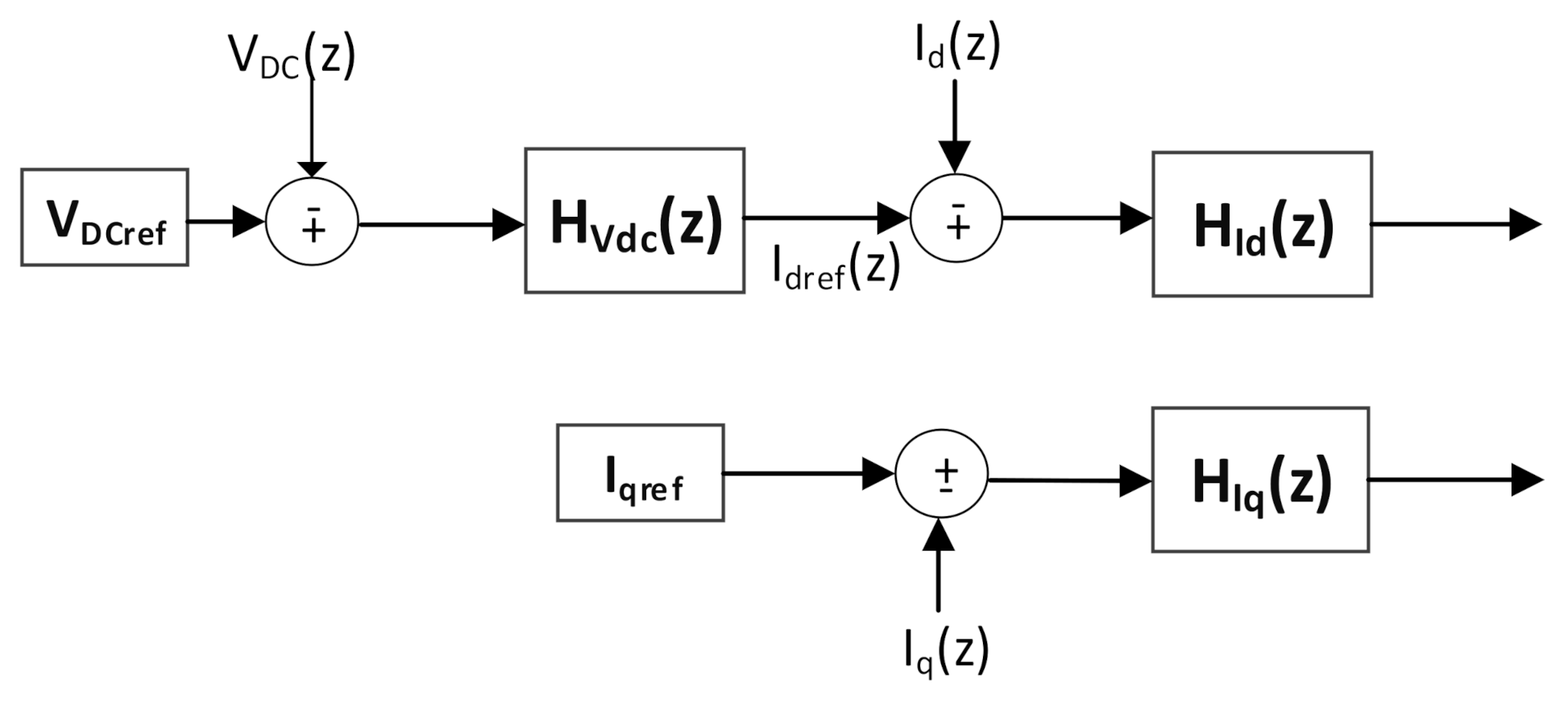
3.2. Control Design and Optimization

The control system of the charger delivered DC voltage regulation. The approach adjusted the required voltage according to charging demand and checked the amount of line current passing through the converter and its ripple. The PWM signals for the six switches of the three-phase AC–DC converter inside the off-board charger were generated by the control system. As shown in Figure 4, the control consisted of an outer DC bus voltage control loop and an inner dq-current control loop. In control design optimization, control performance was optimized by tuning control gains to achieve appropriate overshoot, undershoot, rise time, and settling time. In addition, different types of controllers were designed and implemented in simulation to find a suitable controller for this application, namely PI, Lead-League, PR, and MPR controllers.
Three controllers were used in the classic control of DC voltage and current for three-phase AC–DC converters. One outer-loop voltage controller tracked Vdc [V], and the other two inner-loop current controllers were for Id and Iq [A]. One of the transformation methods, such as the zero-order hold (ZOH), Tustin’s, and modal methods, was used to discretize the continuous-time multi-input multi-output (MIMO) model. Two methods of transformation were utilized here such as Tustin’s and modal methods. The digital z-domain controller was designed by means of methods such as the continuous-time frequency response. Figure 4 provides the complete dual outer and inner loop, comprising the voltage and current controller. A controller was constructed by means of a linear model with the inclusion of sensor delays and computational delays [23].
The overshoot, rise time, settling time, integral absolute error (IAE), and integral time absolute error (ITAE) could all be reduced by tuning the controller using an optimization algorithm [24].
The state-space linear model of the AFE converter was used to design PI controllers in this study. The first-order differential equation was used to derive the AFE converter’s state-space model in the reference dq frame [22]. The closed-loop control design included the sensors and PWM delays, i.e., 10 µs for voltage sensor (LEM DVC 1000-P) delay, 3 µs for current sensor (ISB-425-A-802), and 0.5 µs for PWM. After a close-loop analysis, the PI controller was tuned according to margins and frequencies. The inner loop current PI controllers were designed at <1/10 of the switching frequency, and the outer closed-loop voltage control was designed at 50 Hz line frequency. The gain margin (gM) at the gain crossover frequency (ωcg) and phase margin (PM) at the phase crossover frequency (ωcp) of the voltage control were 22.3   dB   at ( 2.11 × 10 3   rad / s ) and 58° at ( 346   rad / s ), and of the current control were 33.9   dB   at ( 3.17 × 10 5   rad / s ) and 51° at ( 1.73 × 10 3   rad / s ).
Then, in an offline (closed-loop linear model) and online (closed-loop simulation model) setup, their results were compared. At a minimum value of the objective function, i.e., ITAE and IAE of the voltage error, the controller’s robustness could be achieved. The PI, lead–lag, PR, and MPR control of current controllers were designed at the same margins and frequencies, as shown in the Bode plot in Figure 5. Then, their performances were compared in an offline (with closed-loop linear model) and online (closed-loop simulation model) setup. The robustness of the controller could be observed at a minimum value of the objective function, i.e., ITAE and IAE of the voltage error. The transfer functions of the PI, lead–lag, PR, and MPR controls [2,24,25,26,27] are shown in Table 2. This analysis of ITAE and IAE of the voltage error was carried out in a non-linear simulation of the charger and is shown in Table 3. The transfer functions of controllers, gM, PM, ωcp, and ωcg, are also tabulated in Table 3.
For the PR control, the proportional gain K p related the system’s dynamic response, the resonant gain K r regulated the phase shift of reference and output, and resonant frequency ω 0 was set to 50 Hz (314.16 rad/s). In the procedure of design of MPR control, four parameters were considered: proportional gain K p , resonant gain K r , ω c , and ω 0 . The resonant frequency ω 0 can be considered as 50 Hz (314.16 rad/s). All control transfer functions are elaborated on in Table 2 [18,19,20,21]. The control design parameters of all controllers are illustrated in Table 3.
In addition, a closed-loop linear model was used to perform a disturbance rejection analysis. In the presence of input and output disturbances, it provided information about the designed controller. When a disturbance entered a system, the disturbance rejection plot could reveal information about the controller’s effectiveness. The system responded quickly to controller disturbances in order to return to a stable state. Figure 6a shows a block diagram of input/output disturbance rejection and a comparison of the PI, lead–lag, PR, and MPR controls in a closed-loop input/output disturbance rejection.
In the closed-loop Bode response comparison of all current controllers, displayed in Figure 5, the magnitude and frequency responses of the PI, lead–lag, PR, and MPR controllers were identical because all controllers were designed at the same gM, PM, ωcp, and ωcg. However, the disturbance rejection response of the outer loop voltage controller with the PI and lead–lag was different from the PR and MPR controls, as shown in Figure 6b. From all the above results, it was determined that the PI and lead–lag behaved equally. The PRC and MRPC responses, on the other hand, were slow, with a lot of overshoot and settling time. They were then implemented in a non-linear simulation after discretization of the sample time, as shown in the next section of simulation results. To gain more justification, a thorough comparison analysis of the PI, lead–lag, PR, and MPR controls was carried out.

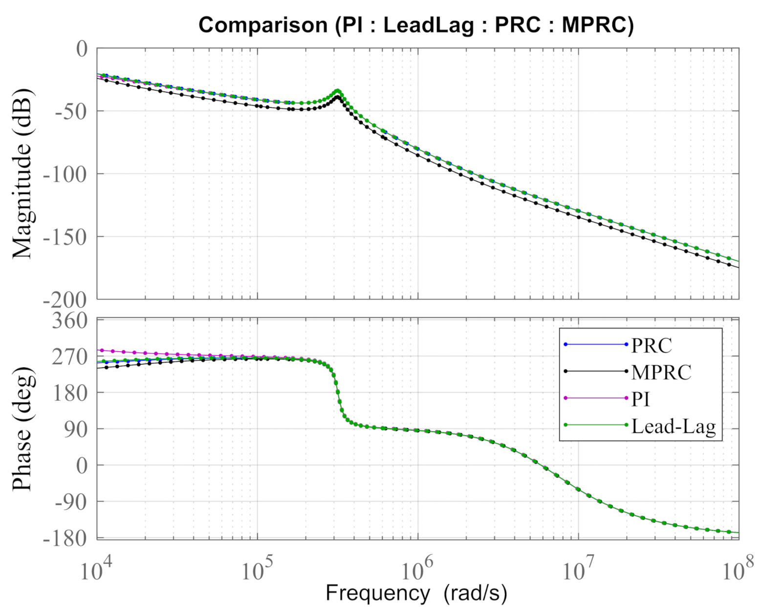
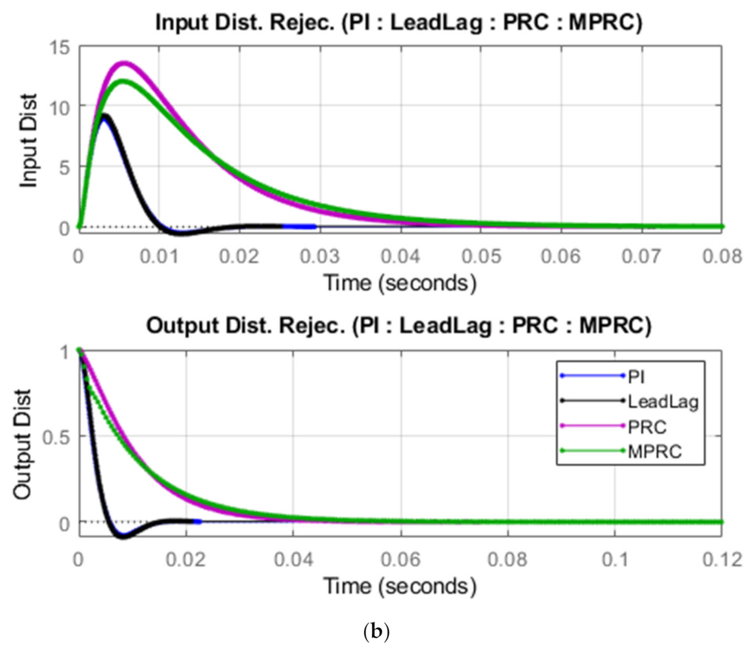
4. Simulation Results

A simulation model for the off-board charger was developed to check the dynamic performances of the controller. Two major analyses were conducted in the simulation model: reference tracking and a disturbance rejection analysis. All simulation results were generated according to the parameters as shown in Table 3.
Different AC faults were injected into the simulation in the dynamic disturbance analysis to check the controller’s behavior during and after a fault. For analysis and validation of controller performance, single-phase-to-line faults (1-line–ground), two-phase-to-line faults (2-line–ground), three-phase-to-line faults (3-line–ground), and line-to-line faults (line–line) were considered. Grid AC voltage and AC current during faults are shown in Figure 7.
The simulation results of the designed controllers are depicted in Figure 8. In this plot, red is the reference command, blue is the PI, black is lead–lag, magenta is PR, and green is MPR-based control. Initially, the DC reference was set to 650 V with no load. From 0 to 3.3 s, the converter related to the DC link capacitor pre-charge circuit, and after 3.3 s, the DC link capacitor was directly connected to the converter. At 3.5 s, a DC resistive load was connected to the converter. During this interval, PWM controller signals were not enabled and the system operated as a diode rectifier. At 3.8 s the controller was enabled, and it tracked the reference DC voltage of 650 V. Then, the DC reference changed from 650 V to 750 V at 4 s. In the results, all controllers follow the reference voltage command, but every controller has its own profile, as shown in Figure 8. Furthermore, step-by-step AC faults were inserted into the system to check the capability of the controllers. Faults of 1 line–ground, 2 line–ground, 3 line–ground and line–line were injected at different times: 4.2, 4.45, 4.7, and 4.95 s, respectively. The controllers performed well in all cases but had nonidentical overshoot, rise time, settling time, ITAE, and IAE.
Table 3 and Figure 8 summarize the simulation results, which show that the PI and lead–lag behaved similarly and had less overshoot, rise time, settling time, ITAE, and IAE. PRC and MRPC responses, on the other hand, were unsatisfactory due to higher overshoot, ITAE, and IAE. As a result, both PI and lead–lag could be used to implement RT. In comparison to lead–lag, PI control on RT–FPGA is relatively simple to implement. As a result, for RT implementation, the PI controller was chosen.
The THD of the line current with the PI control was also estimated and observed at less than 5% at full load and at 20% of full load; the THD analysis is shown in Figure 9. The THD of the line current was calculated using the MATLAB Powergui tool of FFT analysis. The general mathematical representation of THD is as follows in Equation (10), the ratio between the root mean square (RMS) of harmonic magnitude and RMS magnitude of the fundamental frequency of 50 Hz.
THD = Total   RMS   current   of   harmonics RMS   current   of   fundamental =   n = 2 5 I n 2 I 1 × 100   %  

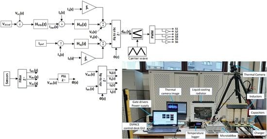
5. Real-Time Control Implementation

This paper now introduces the practical RT implementation of the controller correlated with the XSG program. The controller of the off-board charger was designed in the z-domain, as depicted in Figure 8. An experimental setup was developed and employed in the laboratory to validate the controller’s robustness. A dSPACE MicroLabBox with an embedded hardware board of Xilinx Kintex-7 XC7K325T FPGA was utilized to implement the control strategy [17]. The discrete control is shown in in Figure 10.

5.1. Controller Sampling Time

The period clock of the FPGA of dSpace MicroLabBox was 10 ns. Therefore, the output digital PWM signals were generated at a sampling time of 10 ns. The controllers, analog sensing measurements, sensor filters, PLL, carrier wave, and all calculations (i.e., abc-dq0, dq0-abc, and trigonometric calculation) were performed at a sampling time of 10µsec. The FPGA block was designed in MATLAB/Simulink for the sampling time of the controller, as shown in Figure 11.

5.2. Sensors Calibration

5.2.1. Voltage Sensors

The analog voltage sense transducer (DVC 1000-P) was used for three-phase AC and DC voltage measurements. This voltage transducer gave output voltage in the range of 0 to 5 V maximum. The scaling factor of the sensors was calculated for the implementation of the RT controller (MicroLabBox). The 16-bit data came from the analog port of dSpace MicroLabBox of maximum (±10 V or ± 2 16 2 ). The voltage transducer’s output was connected to the analog input port of MicrolabBox. The analog input of the voltage sensor was multiplied with a factor 10 32 , 676 to convert it into the sensor output voltage [V] for the measurement of maximum ± 1888 V. The scaling factor for the accurate voltage measurement is further elaborated on in Equation (11). Moreover, a 10th order moving average filter was integrated to wash out the noise of voltage sensors.
Actual   Voltage   V   =   Sensor   Voltage out 2.498   ×   754.6

5.2.2. Current Sensors

The analog current sense transducer (ISB-425-A-YZZ) was used for three-phase AC and DC current measurements. This current sensor gave an output voltage in the range of 0 to maximum 5 V according to the factor of 4.706 mV/A. The scaling factor of the current sensors was calculated for the implementation of the RT controller (MicroLabBox). Similar to the voltage sensor, the 16-bit data came from the analog port of dSpace MicroLabBox of maximum (±10 V or ± 2 16 2 ). The current transducer output was connected to the analog input port of MicrolabBox. The analog input of the current sensor was multiplied with a factor 10 32 , 676 to convert it into a sensor output voltage [V] for the measurement of maximum ±528 A. The scaling factor for the accurate current measurement is illustrated in Equation (12). Moreover, a 10th order moving average filter was integrated at the output of this block to wash out the noise of current sensors.
Actual   Current   A   =   Sensor   Voltage out 2.4825   ×   212.5

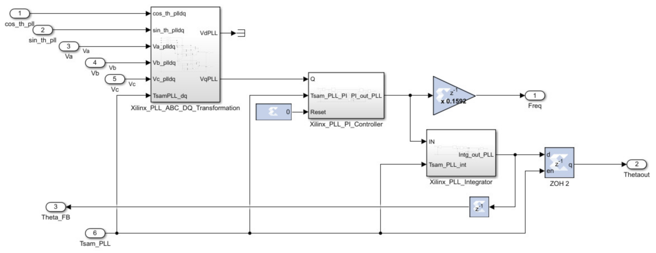
5.3. Phase Lock Loop (PLL)

A PLL was used to calculate the phase angle and fundamental frequency based on the zero voltage crossing for the synchronization of converters to the AC grid. Furthermore, the PLL was also utilized for grid synchronization, and for controlling and estimating state variables. PLL-based synchronization techniques are the most conventional and widely accepted [28,29]. Hence, RT–PLL was implemented on an FPGA to estimate the grid frequency and angle of three-phase grid voltages. The phase angle of the PLL was further used for Clarke (abc to dq0) and Park (dq0 to abc) transformations. The FPGA-based PLL implementation block is shown in Figure 12.

5.4. PI Controller

Discrete PI controllers were implemented in RT–FPGA for dual-loop control, i.e., DC voltage (HVdc(z)), Id (HId(z)), and Iq (HIq(z)) controls as shown in Figure 13. The outer voltage loop in the dual-loop control structure generated the reference current for the inner control loop of the current. Using methods similar to continuous-time frequency response methods, the digital PI controller was designed directly in the z-domain [23]. The transfer function of the digital z-domain PI controller is represented in Equation (13); T s is the sampling time of the controller.
H z   = K p + K i T s z z 1

5.5. Clarke/Park Transformation
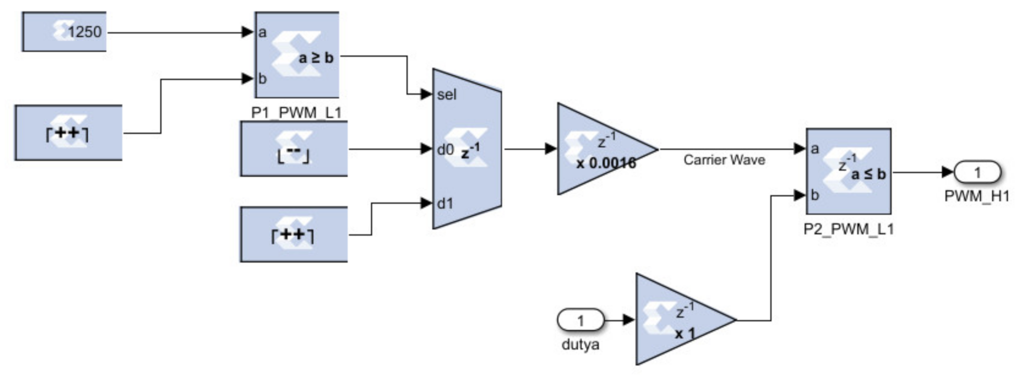
The transformation blocks (i.e., abc to dq0 and dq0 to abc) were designed and implemented in RT–FPGA for voltage and current measurements. The following equations were implemented for dual loop voltage and current control design: Equations (14) and (15) for abc-to-dq transformation, and Equations (16)–(18) for dq-to-abc transformation.
V d = 2 3 Sin θ   V a + 1 2 ( Sin θ     3   Cos θ ) V b + 1 2 ( Sin θ   +   3   Cos θ ) V c  
V q = 2 3 Cos θ   V a + 1 2 ( Cos θ   +   3   Sin θ ) V b + 1 2 ( Cos θ     3   Sin θ ) V c  
V a = Cos θ   V q + Sin θ   V d
V b = 1 2 ( Sin θ     3   Cos θ ) V d + 1 2 ( Cos θ   +   3   Sin θ ) V q
V c = V a V b

5.6. PWM Signals

The controller was designed at a switching frequency of 40 kHz. Therefore, a triangular wave was generated in RT–FPGA at 40 kHz. The amplitude of the triangular wave was 2 (by multiplying with 0.0016). In addition, this triangular wave was used to generate 40 kHz PWM signals by comparing it with the controller’s duty cycle (magnitude between 0 and 2), as shown in Figure 14.

6. Experimental Setup and Results

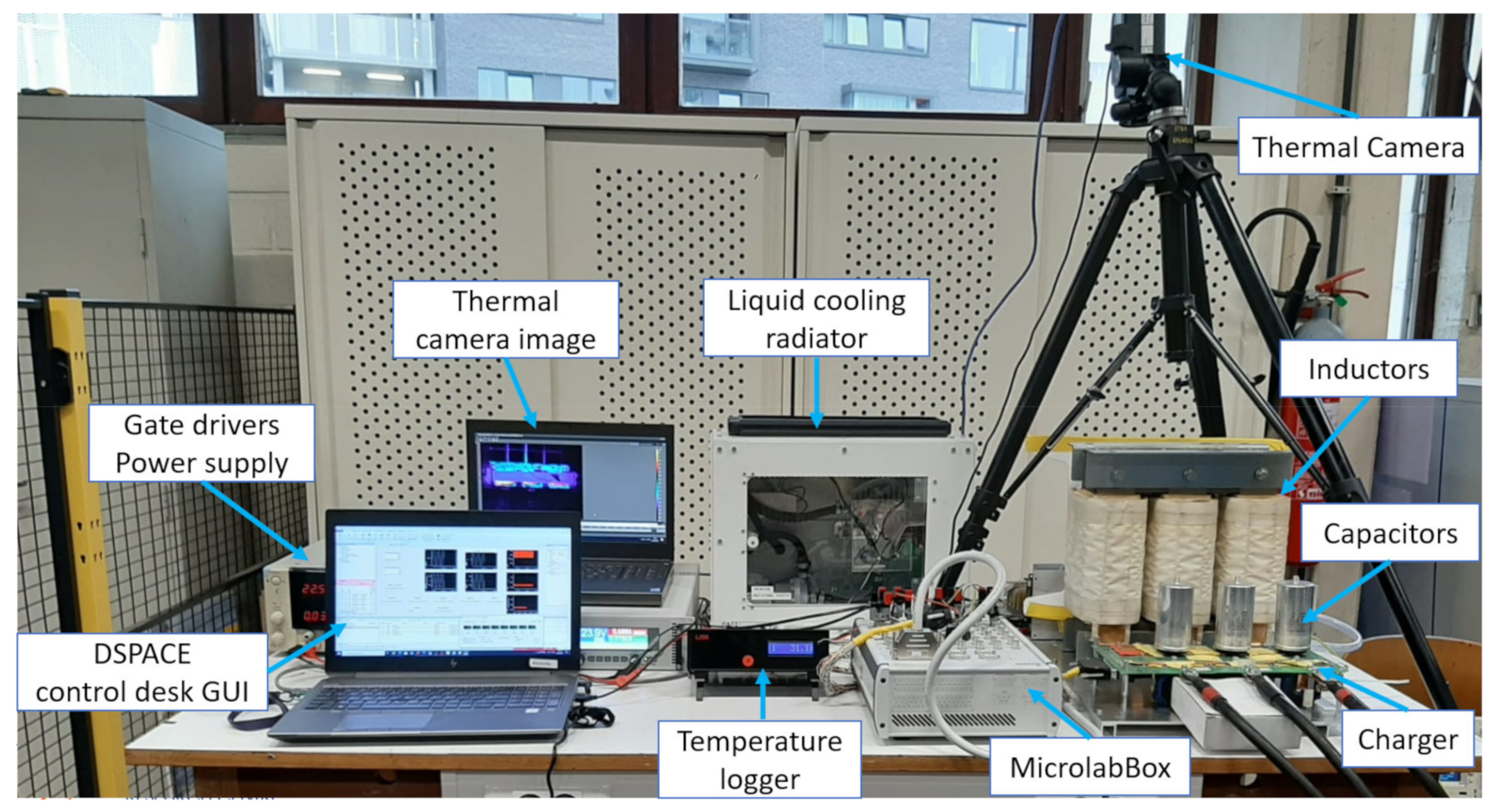
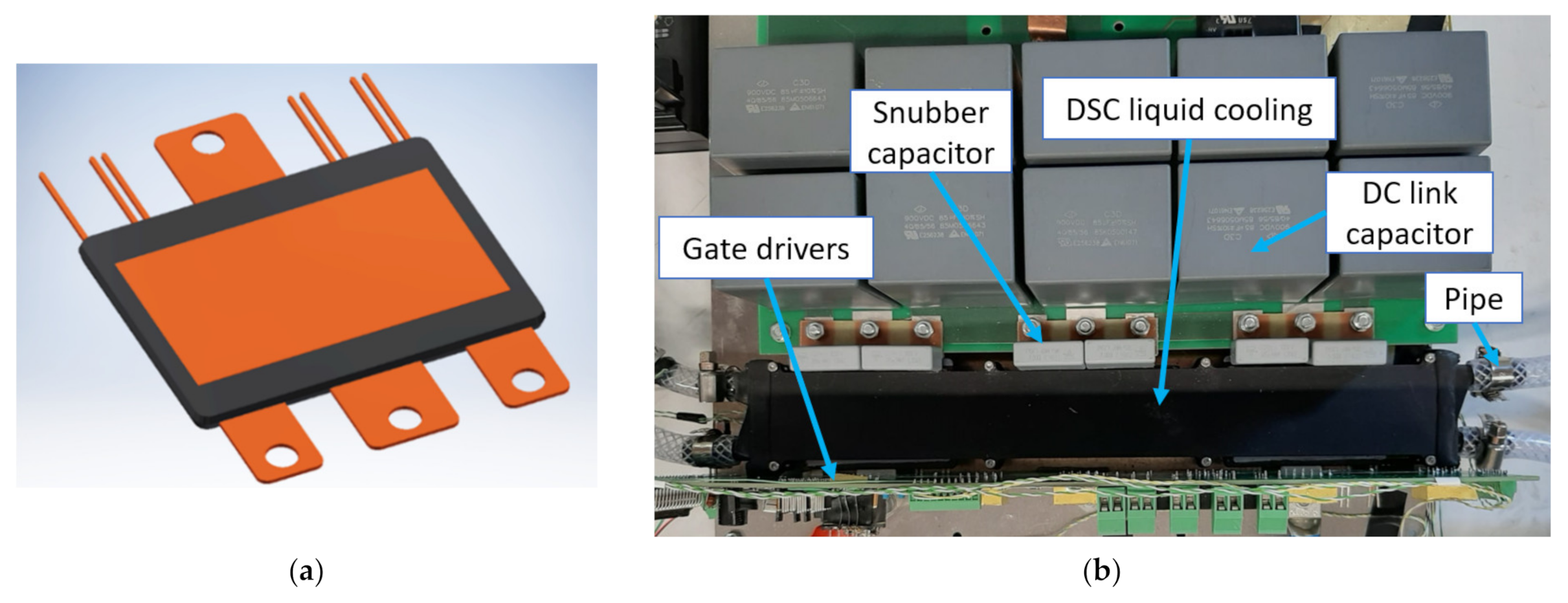
6.1. Experimental Setup

A three-phase AC grid and a DC resistive load were connected to create the test setup. The off-board charger was powered by a three-phase grid. The three LC filters of 100 uH–10 uF were connected on the grid side of the converter, as depicted in Figure 15. Ten DC link capacitors of 85 uF were connected on the DC side of the converter as shown in Figure 16b. Two snubber capacitors of 220 uF were connected at the drain–source of each half-bridge module. Four analog voltage transducers (DVC 1000-P) and four current transducers were used to measure current and voltage on both the DC and AC sides of the charger (ISB-425-A-YZZ). For testing, the lab resistor bank was used as a DC load. A double-sided liquid cooling system was connected to the radiator as shown in Figure 15 and Figure 16b, and all temperature data were logged on a computer drive by temperature sensors and an infrared thermal camera. The SiC technology-based Infineon double-sided half-bridge power electronics (PE) modules and the dual-sided liquid cooling system, explicitly developed for the HiPerform EU project, are shown in Figure 16a,b. For the generation of 40 kHz PWM square wave signals, the real-time controller was implemented on the dSpace MicroLabBox. The dSpace GUI was designed to provide reference commands, monitoring, and measurements, such as DC voltage, DC current, and three-phase AC voltage and current. All experimental data was logged in the computer database. The testing setup of the charger is shown in Figure 15.

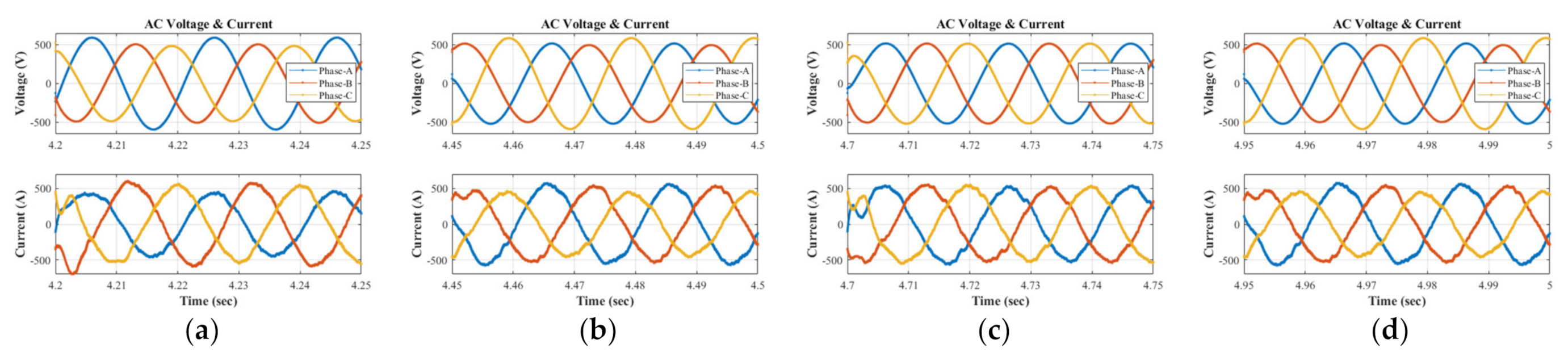
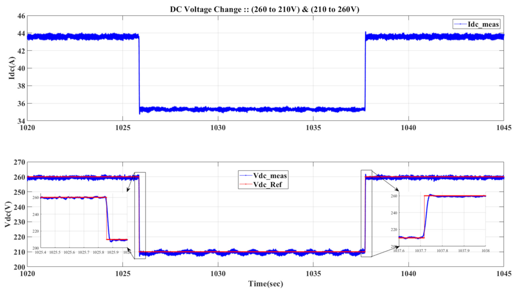
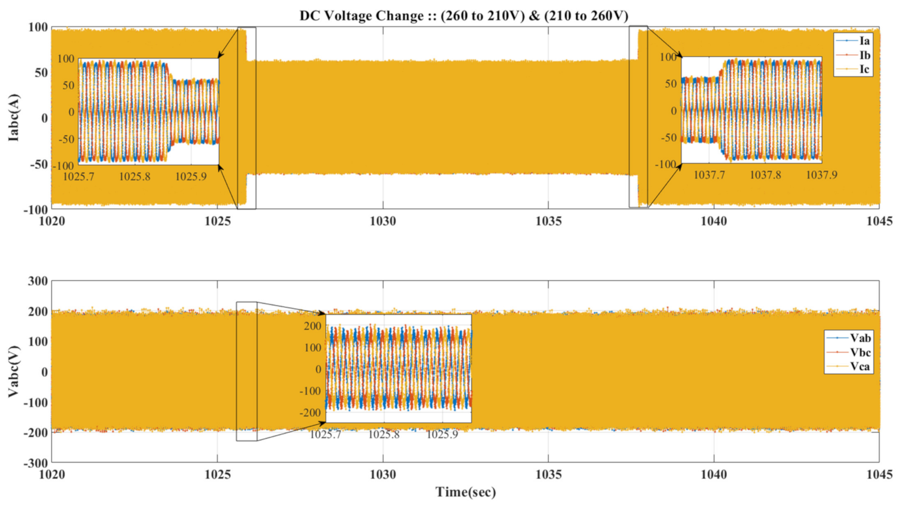
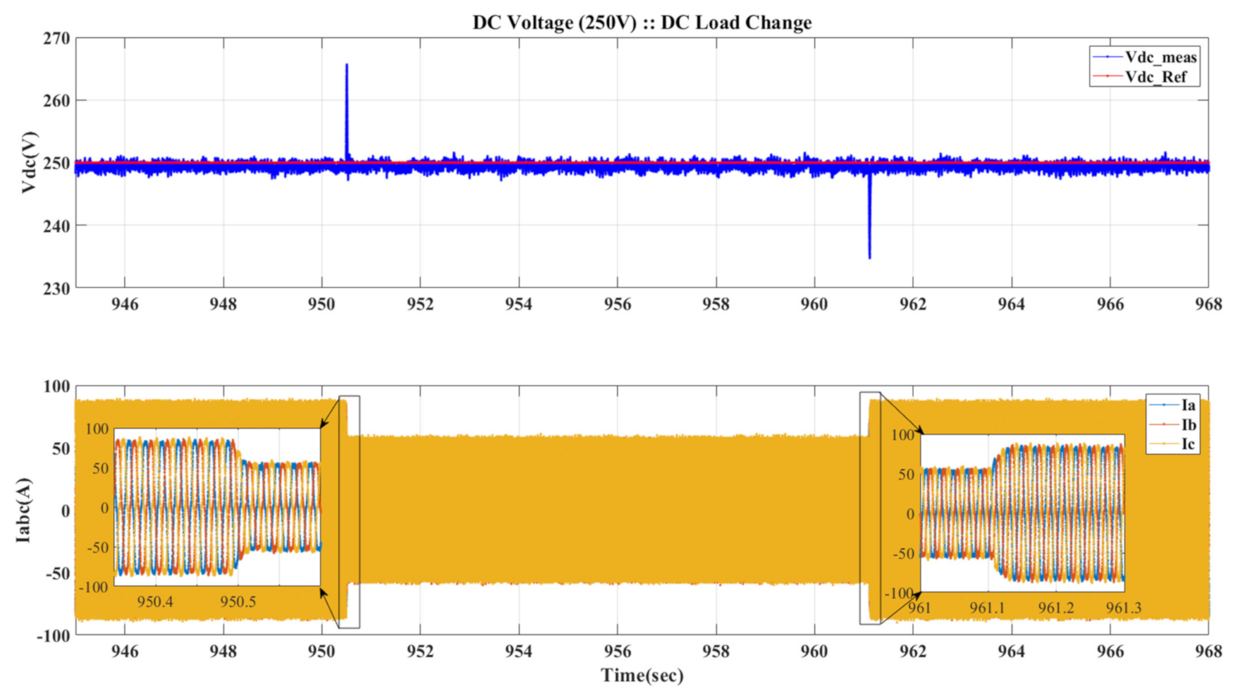
6.2. Experimental Results

The real-time off-board charger voltage–current controller was implemented on the FPGA of dSpace MicroLabBox at 40 kHz switching frequency. The data acquisition was made with MicroLabBox. The charger’s voltages, currents, and enable flags data were logged at a sampling frequency of 0.1 kHz. The logged parameters included line-to-line voltages vab, vbc, vca [V], three-phase currents ia, ib, ic [A], and DC input current idc [A] and voltage Vdc [V].
The goal of the test was to ensure that the controller worked properly in the experimental setup. As a result, this test was carried out at one third of the 400 V phase voltage. The controller’s performance was put to the test in two ways. By changing the reference command to 50 V in test 1, DC voltage reference tracking was tested. Figure 17 and Figure 18 show the DC and AC current and voltage responses, respectively. In test 2, a variation of the DC load was tested at a fixed voltage reference. DC voltage and three-phase AC current responses are depicted in Figure 19. The controller was practically observed to track the reference signal in both tests successfully. Two spikes of 15 V in measured DC voltage in Figure 19 occurred because of the sudden change of load. The resistive load increased at 950 s and then reduced to the initial state at 961 s. The resistive load increased at 950 s and then reduced to the initial state at 961 s. The THD of the line current from experimental data was 4.97%, as depicted in Figure 20, and efficiency was 97% at 12 kW power.

7. Conclusions

In this paper, the modeling, design control, and implementation of a next-generation SiC-based off-board charger for BEBs are described. Such charging infrastructure will be required in the near future to deal with the growing number of BEBs in cities and their heavy load on the electricity grid. SiC switches operate at a high switching frequency and allow for high energy savings and better power quality compared to Si-technology. Nonetheless, dealing with their fast dynamics necessitates accurate modeling and control design. Therefore, a linear and non-linear MATLAB simulation model of the off-board charger were developed. System performance was verified in simulation through the evaluation of reference tracking, system ripples, and THD of the line current. Four types of controllers, i.e., PI, lead–lag, PR, and MPR, were designed with a linear model and validated in a non-linear simulation model. In terms of performance and RT implementation, it is concluded that the PI controller is a better choice than other controllers. The designed controller had a gain margin of 22.3, a phase margin of 58°, and achieved a minimum ITAE of 19.70 and IAE of 85.95. The line current THD was below 5% and the PF above 99%. A dual-loop voltage and current control were successfully implemented and tested on the FPGA of a dSpace MicroLabBox at 40 kHz switching frequency. The provided experimental results of the control system demonstrated the correct operation of the real-time implementation of the controller by tracking the reference command, thus enabling the off-board charger for BEBs used in public transport.
As the infrastructure of charging plays a key role in the deployment of BEBs, robust control design is essential to achieve a highly efficient and reliable fast-charging system. Nevertheless, proper control architecture design still needs to be developed for a bidirectional operation, i.e., the V2G and G2V of the chargers and the correction of unbalanced voltage in the grid, with the implementation of controls for WBG devices operating at high switching frequencies. This will need to be tackled in future research.

Author Contributions

Conceptualization, H.R.; formal analysis, H.R.; investigation, H.R., B.V., S.J, E.A., T.G., M.E.B. and O.H.; writing—original draft preparation, H.R., B.V., S.J. and E.A.; writing—review and editing, T.G., M.E.B. and O.H.; visualization, H.R.; supervision, O.H. All authors have read and agreed to the published version of the manuscript.

Funding

This work was supported by project HiEFFICIENCT. This project has received funding from the ESCEL joint undertaking (JU) under Grant Agreement no. 101007281. The ESCEL JU receives support from the European Union’s horizon 2020 research and innovation programme and Austria, Germany, Slovenia, Netherlands, Belgium, Slovakia, France, Italy, and Turkey.

Acknowledgments

Authors also acknowledge Flanders Make for the support to our research group.

Conflicts of Interest

The authors declare no conflict of interest.

References

  1. Yilmaz, M.; Krein, P.T. Review of integrated charging methods for plug-in electric and hybrid vehicles. In Proceedings of the 2012 IEEE International Conference on Vehicular Electronics and Safety (ICVES 2012), Istanbul, Turkey, 24–27 July 2012; pp. 346–351. [Google Scholar]
  2. Hegazy, O.; Van Mierlo, J.; Lataire, P. Design and control of bidirectional DC/AC and DC/DC converters for plug-in hybrid electric vehicles. In Proceedings of the 2011 International Conference on Power Engineering, Energy and Electrical Drives, Malaga, Spain, 11–13 May 2011; pp. 1–7. [Google Scholar]
  3. Monteiro, V.; Pinto, J.G.; Exposto, B.; Gonçalves, H.; Ferreira, J.C.; Couto, C.; Afonso, J.L. Assessment of a battery charger for electric vehicles with reactive power control. In Proceedings of the IECON 2012—38th Annual Conference on IEEE Industrial Electronics Society, Montreal, QC, Canada, 25–28 October 2012; pp. 5142–5147. [Google Scholar]
  4. Microsemi, P.P.G. Gallium Nitride (GaN) Versus Silicon Carbide (SiC) in the High Frequency (RF) and Power Switching Applications. Digi-Key. 2014. Available online: https://www.google.com.hk/url?sa=t&rct=j&q=&esrc=s&source=web&cd=&ved=2ahUKEwj9pMrCsoP2AhVWAd4KHei6Ca4QFnoECAQQAQ&url=https%3A%2F%2Fwww.richardsonrfpd.com%2Fdocs%2Frfpd%2FMicrosemi-A-Comparison-of-Gallium-Nitride-Versus-Silicon-Carbide.pdf&usg=AOvVaw04OQ1N7lQjVwJm-D6NBe2e (accessed on 10 February 2022).
  5. Rasool, H.; El Baghdadi, M.; Rauf, A.M.; Zhaksylyk, A.; Hegazy, O. A Rapid Non-Linear Computation Model of Power Loss and Electro Thermal Behaviour of Three-Phase Inverters in EV Drivetrains. In Proceedings of the 2020 International Symposium on Power Electronics, Electrical Drives, Automation and Motion (SPEEDAM), Sorrento, Italy, 24–26 June 2020; pp. 317–323. [Google Scholar]
  6. Chakraborty, S.; Vu, H.-N.; Hasan, M.M.; Tran, D.-D.; El Baghdadi, M.; Hegazy, O. DC-DC converter topologies for electric vehicles, plug-in hybrid electric vehicles and fast charging stations: State of the art and future trends. Energies 2019, 12, 1569. [Google Scholar] [CrossRef] [Green Version]
  7. Rasool, H.; Verbrugge, B.; Zhaksylyk, A.; Tran, T.M.; El Baghdadi, M.; Geury, T.; Hegazy, O. Design Optimization and Electro-thermal Modelling of an Off-Board Charging System for Electric Bus Applications. IEEE Access 2021, 9, 84501–84519. [Google Scholar] [CrossRef]
  8. Verbrugge, B.; Hasan, M.M.; Rasool, H.; Geury, T.; El Baghdadi, M.; Hegazy, O. Smart Integration of Electric Buses in Cities: A Technological Review. Sustainability 2021, 13, 12189. [Google Scholar] [CrossRef]
  9. Rasool, A.; Yan, X.; Rasool, U.; Abbas, F.; Numan, M.; Rasool, H.; Jamil, M. Enhanced control strategies of VSG for EV charging station under a low inertia microgrid. IET Power Electron. 2020, 13, 2895–2904. [Google Scholar] [CrossRef]
  10. Seth, A.K.; Singh, M. Modified repetitive control design for two stage off board Electric Vehicle charger. ISA Trans. 2021. [Google Scholar] [CrossRef] [PubMed]
  11. Verbrugge, B.; Rasool, H.; El Baghdadi, M.; Geury, T.; Hegazy, O. Modelling and bi-level control design of a SiC off-board charging system for battery electric buses with V2G capability. In Proceedings of the 2021 23rd European Conference on Power Electronics and Applications (EPE’21 ECCE Europe), Ghent, Belgium, 6–10 September 2021; pp. 1–10. [Google Scholar]
  12. Chakraborty, S.; Rasool, H.; Tran, D.-D.; Geury, T.; El Baghdadi, M.; Hegazy, O. Design and Implementation of a Multifunctional 6-phase Interleaved Bidirectional DC/DC Converter for Battery Electric Vehicle Applications. In Proceedings of the 2021 23rd European Conference on Power Electronics and Applications (EPE’21 ECCE Europe), Ghent, Belgium, 6–10 September 2021; pp. 1–10. [Google Scholar]
  13. Selvamuthukumaran, R.; Gupta, R. Rapid prototyping of power electronics converters for photovoltaic system application using Xilinx System Generator. IET Power Electron. 2014, 7, 2269–2278. [Google Scholar] [CrossRef]
  14. Cherragui, H.; Hilairet, M.; Giurgea, S. Hardware-in-the-loop simulation of a boost converter with the Xilinx System Generator from Matlab/Simulink. In Proceedings of the IECON 2015—41st Annual Conference of the IEEE Industrial Electronics Society, Yokohama, Japan, 9–12 November 2015; pp. 1837–1842. [Google Scholar]
  15. Kumari, B.; Rana, R.S.; Patil, C.Y. FPGA and dspace based sliding mode control of boost converter for pem fuel cell application. Int. J. Comput. Appl. 2012, 51, 4–10. [Google Scholar] [CrossRef]
  16. Thangavelu, A.; Varghese, M.V.; Vaidyan, M.V. Novel FPGA based controller design platform for DC-DC buck converter using HDL Co-simulator and Xilinx System Generator. In Proceedings of the 2012 IEEE Symposium on Industrial Electronics and Applications, Bandung, Indonesia, 23–26 September 2012; pp. 270–274. [Google Scholar]
  17. Tran, D.-D.; Geury, T.; El Baghdadi, M.; Van Mierlo, J.; Hegazy, O. Design and Implementation of FPGA-based Digital Controllers for SiC Multiport Converter in Electric Vehicle Drivetrains. In Proceedings of the 2019 21st European Conference on Power Electronics and Applications (EPE’19 ECCE Europe), Genova, Italy, 3–5 September 2019. [Google Scholar]
  18. Battiston, A.; Miliani, E.-H.; Pierfederici, S.; Meibody-Tabar, F. Efficiency improvement of a quasi-Z-source inverter-fed permanent-magnet synchronous machine-based electric vehicle. IEEE Trans. Transp. Electrif. 2016, 2, 14–23. [Google Scholar] [CrossRef]
  19. Chakraborty, S.; Tran, D.-D.; Van Mierlo, J.; Hegazy, O. Generalized Small-Signal Averaged Switch Model Analysis of a WBG-based Interleaved DC/DC Buck Converter for Electric Vehicle Drivetrains. In Proceedings of the 2020 22nd European Conference on Power Electronics and Applications (EPE’20 ECCE Europe), Lyon, France, 7–11 September 2020. [Google Scholar]
  20. Jappe, T.K.; Polla, R.R.; Fuerback, A.L.; Heldwein, M.L.; Soeiro, T.B.; Andrich, R. An FPGA-based single-phase interleaved boost-type PFC rectifier employing GAN HEMT devices. Rev. Eletrônica Potência 2014, 19, 414–422. [Google Scholar] [CrossRef]
  21. Abbas, G.; Gu, J.; Farooq, U.; Abid, M.I.; Raza, A.; Asad, M.U.; Balas, V.E.; Balas, M.E. Optimized Digital Controllers for Switching-Mode DC-DC Step-Down Converter. Electronics 2018, 7, 412. [Google Scholar] [CrossRef] [Green Version]
  22. Rasool, H.; Zhaksylyk, A.; Chakraborty, S.; El Baghdadi, M.; Hegazy, O. Optimal Design Strategy and Electro-Thermal Modelling of a High-Power Off-Board Charger for Electric Vehicle Applications. In Proceedings of the 2020 Fifteenth International Conference on Ecological Vehicles and Renewable Energies (EVER), Monte-Carlo, Monaco, 10–12 September 2020; pp. 1–8. [Google Scholar]
  23. Hegazy, O.; Van Mierlo, J.; Lataire, P. Analysis, Modeling, and Implementation of a Multidevice Interleaved DC/DC Converter for Fuel Cell Hybrid Electric Vehicles. IEEE Trans. Power Electron. 2012, 27, 4445–4458. [Google Scholar] [CrossRef]
  24. Rasool, H.; Rasool, A.; Ikram, A.A.; Rasool, U.; Jamil, M.; Rasool, H. Compatibility of objective functions with simplex algorithm for controller tuning of HVDC system. Ing. Investig. 2019, 39, 34–43. [Google Scholar] [CrossRef] [Green Version]
  25. Jamil, M.; Waris, A.; Gilani, S.O.; Khawaja, B.A.; Khan, M.N.; Raza, A. Design of robust higher-order repetitive controller using phase lead compensator. IEEE Access 2020, 8, 30603–30614. [Google Scholar] [CrossRef]
  26. Kumar, N.; Saha, T.K.; Dey, J. Control, implementation, and analysis of a dual two-level photovoltaic inverter based on modified proportional–resonant controller. IET Renew. Power Gener. 2018, 12, 598–604. [Google Scholar] [CrossRef]
  27. Garcés Quílez, M.; Abdel-Monem, M.; El Baghdadi, M.; Yang, Y.; Van Mierlo, J.; Hegazy, O. Modelling, analysis and performance evaluation of power conversion unit in g2v/v2g application—A review. Energies 2018, 11, 1082. [Google Scholar] [CrossRef] [Green Version]
  28. Giri, A.K.; Arya, S.R.; Maurya, R.; Babu, B.C. VCO-less PLL control-based voltage-source converter for power quality improvement in distributed generation system. IET Electr. Power Appl. 2019, 13, 1114–1124. [Google Scholar] [CrossRef]
  29. Rasool, A.; Yan, X.; Rasool, H.; Guo, H.; Asif, M. VSG stability and coordination enhancement under emergency condition. Electronics 2018, 7, 202. [Google Scholar] [CrossRef] [Green Version]
Figure 1. Characteristics of Si, SiC, and GaN.
Energies 15 01434 g001
Figure 2. Off-board charger topology.
Energies 15 01434 g002
Figure 3. Circuit and control diagram of the SiC off-board charger.
Energies 15 01434 g003
Figure 4. Classical dual-loop control of charger.
Energies 15 01434 g004
Figure 5. Bode plot comparison of PI, lead–lag, PRC, and MPRC.
Energies 15 01434 g005
Figure 6. Disturbance rejection; (a) block diagram, (b) comparison of PI, lead–lag, PRC, and MPRC.
Energies 15 01434 g006aEnergies 15 01434 g006b
Figure 7. 3–phase AC faults; (a) 1 line–ground, (b) 2 line–ground, (c) 3 line–ground and (d) line–line.
Energies 15 01434 g007
Figure 8. DC voltage and current comparison of PI, lead–lag, PRC, and MPRC controllers at 175 kW.
Energies 15 01434 g008
Figure 9. THD of line current; (a) full load, (b) 20% load following the standards < 5%.
Energies 15 01434 g009
Figure 10. Digital control FPGA implementation.
Energies 15 01434 g010
Figure 11. Block for sampling time (10 µs).
Energies 15 01434 g011
Figure 12. Phase lock loop (PLL).
Energies 15 01434 g012
Figure 13. PI controller for voltage and current.
Energies 15 01434 g013
Figure 14. PWM generation.
Energies 15 01434 g014
Figure 15. Off–board charger test setup.
Energies 15 01434 g015
Figure 16. AFE with liquid cooling; (a) half–bridge DSC module, (b) DSC modules with plates.
Energies 15 01434 g016
Figure 17. Test 1: DC voltage reference tracking.
Energies 15 01434 g017
Figure 18. Test 1: Three–phase AC voltages and currents.
Energies 15 01434 g018
Figure 19. Test 2: DC voltage and three–phase AC currents.
Energies 15 01434 g019
Figure 20. Experimental THD of line current.
Energies 15 01434 g020
Table 1. Charger specifications.
ParametersValue
Power (P, kW)175
Line frequency (fAC, Hz)50
Switching frequency (fsw, kHz)40
AC voltage (VAC, V)400
DC Voltage (Vdc, V)600–800
Rectifier inductor (Lrect, uH)100
Grid inductor (Lgrid, uH)1
Capacitor (Cf, uF)10
Damping resistance (rd, Ohm)0.04
DC capacitor (Cdc, mF)0.85
Table 2. Generalized controllers.
ControllerGeneralized Transfer Function
PI K p + K i s
Lead–Lag α s + ω 0 α s + ω 0 α
180 ° < θ < 180 ° ,
α = 1 + sin θ 1 Sin   θ
Proportional Resonance K p + 2 K r s s 2 + ω 0 2
ω 0 = 2 π f   rad / s ,
Modified Proportional Resonance K p + 2 K r ω c s s 2 + 2 ω c s + ω 0 2
ω 0 = 2 π f   rad / s ,
ω c = π ± 10 % f rad / s  
Table 3. Controller design parameters.
ControllerControl ParametersTransfer FunctionGM
(dB)
PM
(deg)
Wcp
(rad/s)
Wcg
(rad/s)
ITAEIAE
Id/Iq
Current Control
Kp = 0.08, Ki = 520 0.08 s + 6500 s 33.9511.73 × 1033.17 × 10585.9519.70
PRC 0.08 s 2 + 25 s + 3.029 × 10 6 s 2 + 3.029 × 10 6 33.9511.74 × 1033.17 × 105126.9428.39
MPRC 0.08 s + 5463 s + 449.2 s 2 + 319.6 s + 2.454 × 10 6 33.9412.2 × 1033.17 × 105127.7828.66
Lead–Lag 0.04476 s + 9721 s + 19.48 39571.61 × 1033.17 × 10587.2319.95
Vdc
Voltage control
Kp = 0.13, Ki = 92 0.13 s + 707.7 s 22.3583462.11 × 10385.9519.70
Publisher’s Note: MDPI stays neutral with regard to jurisdictional claims in published maps and institutional affiliations.

