Article

Oxidized Nickel to Prepare an Inorganic Hole Transport Layer for High-Efficiency and Stability of CH3NH3PbI3 Perovskite Solar Cells

1
Department of Engineering and System Science, National Tsing Hua University, Hsinchu 30013, Taiwan
2
Material and Chemical Research Laboratories, Industrial Technology Research Institute, Hsinchu 31040, Taiwan
3
Department of Chemical and Materials Engineering, Chang Gung University, Taoyuan 33302, Taiwan
4
Department of Pediatrics, Division of Neonatology, Chang Gung Memorial Hospital, Linkou, Taoyuan 33305, Taiwan
5
Green Technology Research Center, Chang Gung University, Taoyuan 33302, Taiwan
6
Department of Chemical and Materials Engineering, National Central University, Jhong-Li, Taoyuan 32001, Taiwan
7
Department of Materials Science and Engineering, City University of Hong Kong, Hong Kong
*
Authors to whom correspondence should be addressed.
These authors contributed equally to this work.
Energies 2022, 15(3), 919; https://doi.org/10.3390/en15030919
Submission received: 7 December 2021 / Revised: 8 January 2022 / Accepted: 17 January 2022 / Published: 27 January 2022
(This article belongs to the Special Issue Advances in Photovoltaic Technologies)

Abstract

:
In this study, we report a perovskite solar cell (PSC) can be benefited from the high quality of inorganic nickel oxide (NiOx) as a hole transport layer (HTL) film fabricated from the physical vapor deposition (PVD) process. The power conversion efficiency (PCE) of PSC is found to depend on the thickness of NiOx HTL. The NiOx thickness is optimized via quantitative investigation of the structure, optical and electrical properties. With an active area of 11.25 cm2, a PSC module (25 cm2) with a PCE of 15.1% is demonstrated, while statistically averaged PCE = 18.30% with an open voltage (Voc) 1.05 V, short-circuit current density (Jsc) 23.89 mA/cm2, and fill factor (FF) 72.87% can be achieved from 36 devices with smaller active areas of 0.16 cm2. After the stability test at 40% relative humidity (RH) and 25 °C for 1200 h, the highest performance NiOx-based PSC is shown to be about 1.2–1.8 times superior to PEDOT:PSS organic HTL based PSC at the same environment.

1. Introduction

Organic–inorganic hybrid perovskite is a very potential material in many application fields, such as organic light-emitting diodes (OLED) [1,2], thin-film transistors (TFT) [3], photodetector [2,3,4], and photovoltaic solar cells [5]. The PCE of organic–inorganic hybrid photovoltaic perovskite solar cell devices has been improved from 3.8% to over 25.5% within recent years [1,2,3,4,5,6]. The photoactive layer CH3NH3PbI3 has a direct bandgap of around 1.5 eV (300–800 nm) with a long carrier diffusion length (>1 μm) [7]. However, the light absorption of a hybrid perovskite can cover visible regime (400–800 nm) with a high extinction coefficient (~104 cm−1 at 550 nm) [8]. The perovskites materials have a crystal structure similar to ABX3. [2,3,4,5,6]. The symbol A is monovalent cation: Methylammonium (MA+), Formamidinium (FA+), and Cesium (Cs+); B is divalent metal cation: Tin (Sn2+) and Lead (Pb2+) and X is halide anion: Iodine (I) or Bromine (Br), respectively [2,3,4,5,6,7,8]. One of the most attractive points for scientists is that these perovskite materials can be synthesized in a low-temperature process with low manufacturing cost that makes the future application more affordable. Usually, a hybrid perovskite solar cell has an inverted (p-i-n structure) configuration given as followed: hole transport layer (HTL)/CH3NH3PbI3/electron transport layer (ETL). In this configuration, the perovskite absorber layer connects to both the HTL and ETL. In an inverted (p-i-n structure) photovoltaic solar cell device, the ETL material must be prepared at the low-temperature process that prevents damaging the perovskite layer. Usually, the solution process 6,6-phenyl C61-butyric acid methyl ester (PCBM) (refs) and evaporated C60 are the most widely used to ETL. However, the disadvantages to PCBM were current leakage, lower electron mobility, and charge recombination with perovskite at the interface [4]. As compared to PCBM, the C60 can be more uniformly cover onto perovskite, which increased electron transport. The performance for inverted (p-i-n structure) PSC with C60 is better than PCBM based for photovoltaic devices. Moreover, the C60 material can be fabricated in either solution process or vacuum thermal evaporation. The vacuum thermal evaporation is applicable for large area fabrication for the ETL layer. In this aspect, the evaporate C60 material is the most widely used to ETL [5,9].
While for HTL, the poly (3,4-ethylene dioxythiophene) poly (styrene-sulfonate) (PEDOT:PSS) is usually used [10,11] as the key materials. The PEDOT:PSS has good conductivity (450 S/cm) and optical transmittance in the visible wavelength range (400–800 nm) [3,10,11,12]. However, the PEDOT:PSS solution is usually acidic. The PEDOT:PSS can cause indium (In) migration into the PEDOT:PSS layer and therefore damage the indium tin oxide (ITO) electrode. In addition, perovskite material basically contains methylamine that can actively react with acid PEDOT:PSS [4,9,10,11,12]. Besides, the PEDOT:PSS material was hygroscopic that damages the interface, and causes a mismatch in work function. Therefore as a role of HTL, the poor stability, high process cost, acidity, and hygroscopicity limit the practical application of PEDOT:PSS on large scale solar devices. In addition, matching the work function of traditional PEDOT:PSS and that of lead iodide-based perovskite greatly set a constraint to the electrical properties of hybrid perovskite solar cells, especially the open-circuit voltage (VOC), which is usually lower than 1.0 V [12].
Compared with HTL made of organic materials, inorganic p-type semiconductors can provide inherently higher stability. As a role of HTL, p-type inorganic (NiOx) has been extensively studied [11,12,13] due to it has wide bandgap (Eg > 3.5 eV) [14,15,16,17], high optical transmittance [18,19,20,21,22], good chemical stability, and an appropriate valence band [23,24,25] better matching with that of CH3NH3PbI3 as compared with (PEDOT:PSS) [26,27,28]. Besides, NiOx has better hole mobility of 2.8 cm2/Vs [29], as compared with NiOx, the PEDOT:PSS is about 1.5 cm2/Vs [30]. NiOx has a highly stable crystal structure that can be prepared by various methods, such as sol-gel [18], electrodeposition [19], spray pyrolysis [30], spin coating [13,24], pulsed laser deposition [31]. The advantages of the sputtering process, are high deposition rate, films uniformity, large area, and reproducibility as compared to the solution process. Therefore, NiOx can be a very potential application for perovskite solar cells as an HTL [21,23,32]. Furthermore, due to the fact that C60 possesses much higher electron mobility (1.6 cm2/Vs) and conductivity (2.3 × 10⁻³ S/cm) than those spin coated PCBM (6.1 × 10⁻² cm2/Vs and 3.2 × 10⁻⁴ S/cm), respectively [33], recently C60 and BCP deposited by vacuum thermal evaporation are more frequently accepted as a preferable ETL [10].
To improve the sustainability and the performance of perovskite solar cells, the organic ETL PCBM, and HTL PEDOT:PSS in an inverted configuration (pin, HTL/ CH3NH3PbI3/ETL) of hybrid perovskite cell, are replaced with the inorganic C60 and NiOx, respectively. In this study, we have fabricated highly efficient inverted (p-i-n structure) perovskite solar cell devices with inorganic HTL and ETL with stackings: FTO/NiOx/CH3NH3PbI3/C60/Bathocuproine (BCP)/Ag. It was reported that the PCEs of perovskite cells composed of solution-coated HTL NiOx on ITO had been demonstrated to be as high as 5.7% and 15% [11,13]. In this study, we have optimized NiOx thickness by quantitatively analyzing its structure, optical and electrical properties. We fabricated 36 devices of perovskite solar cells for reproducibility tests under AM 1.5G illumination. It was demonstrated that the device has an averaged Voc = 1.05 V, Jsc = 23.89 mA/cm2, FF = 72.87%, and PCE = 18.3% from an active area of 0.16 cm2. The durability test showed the lifetime of our perovskite cell can be as long as 1200 h which benefits from a follow-up annealing at high temperature after NiOx is deposited onto a FTO substrate. This follow-up annealing is critical to guarantee a high-quality NiOx film to reach PCE = 18% (active area of 0.16 cm2) and 1200 h lifetime. Furthermore, with the integration of the sputtering process for NiOx, this proposed structure inorganic HTL/CH3NH3PbI3/inorganic ETL can be integrated to be a large scale and sheet-to-sheet process for perovskite solar cells.

2. Experimental and Methods

2.1. Device Structure and Fabrication

Our inverted (p-i-n structure) planar heterojunction perovskite device has a stacking structure shown in Figure 1: FTO/NiOx/CH3NH3PbI3/C60/BCP/Ag. The films of the perovskite device were deposited sequentially as its stacking structure. Two different sizes of devices with an active area of 0.16 cm2 and 11.25 cm2, respectively, were fabricated by the following procedures. Fluorine-doped tin oxide (FTO; 15 Ω/sq1) glass substrates were cleaned with ultra-sonication for 20 min in detergent water, acetone, and isopropanol, sequentially. Then FTO glass was baked for 1 h at 150 °C to remove moisture. After that, the FTO glass was placed in UV-ozone for 20 min.
The NiOx films were deposited onto the FTO glass for several lengths of time (20 s–80 s) by the RF magnetron sputtering method. The nickel target has a size of 2” and has a purity of 99.99%. The target and the substrate were set to be approximately 8 cm apart in the sputtering chamber which was evacuated to a base pressure below 5 × 10⁻⁶ torr before deposition. The power is set to be 200 W, and four film thicknesses were controlled with deposition time set for 20 s, 40 s, 60 s, and 80 s, respectively. NiOx film was formed by annealing the as-deposited nickel film in a quartz tubular oven for 1 h at 500 °C with an oxygen flow of 60 sccm. The solution for preparation of light absorber layer the perovskite layer is a 1.5 M methylammonium lead tri-iodide (MAPbI3) solution, that contains 0.578 g of lead iodide (PbI2, 99.9985%, Alfa Aesar, Hefreer, MA, USA) and 0.196 g methylammonium iodide (MAI) which is dissolved into a mixed solvent containing Dimethyl sulfoxide (DMSO, ≥99.9%, Sigma-Aldrich, St. Louis, MO, USA) and Gamma-Butyrolactone (GBL, ≥99%, Sigma-Aldrich) (DMSO: GBL, 1: 1 volume ratio). This solution was then oscillated and heated at 50 °C for 3 h in an ultra-sonication process. Then the perovskite layer was spin coated onto the NiOx film layer with the one step process that without an anti-solvent wash procedure involved in a nitrogen glove box.
The substrate of FTO/NiOx was baked at 120 °C for 10 min with a hot plate then it was treated in UV-ozone for 15 min. The perovskite film was fabricated by spin coating with MAPbI3 solution at 1000 rpm for 10 s then 3000 rpm for the 30 s. Perovskite film with a thickness of about 340 nm was formed after the sample is baked at 100 °C for 10 min with a hot plate. Followed, thin layers of C60/BCP with thicknesses of 45 nm and 5 nm, respectively, were deposited onto perovskite film. The C60 and BCP are deposited by a process of vacuum thermal evaporation. Finally, silver contact is deposited onto the BCP by the thermal evaporator under a vacuum chamber with a base pressure of 5 × 10⁻⁶ torr for device fabrication. The thickness of the silver electrode is about 100 nm. The active area of two sets of perovskite devices was made to be around 0.16 cm2 and 11.25 cm2, respectively, which was defined with a shadow mask during Ag evaporation. The construction of inverted (p-i-n structure) PSCs is shown in Figure 1a and the energy level of the working principle for inverted perovskite (CH3NH3PbI3) solar cell devices is shown in Figure 1b.

2.2. Equipment Specification

The ex-situ X-ray diffraction patterns were recorded on a high resolution X-ray diffractometer equipped (Bede D1) with Cu-kα that operate conditions are 45 kV and 35 mA, radiation at a scanning rate of 2 °/min. The optical transmittance spectra of NiOX films was recorded with an ultra violate visible (UV-vis) spectrometer (LAMBDA 900, PerkinElmer, Waltham, MA, USA). The surface morphology and cross-section structure used a high-resolution field emission scanning electron microscope (FE-SEM, JSM-7610F, JEOL Ltd., Tokyo, Japan). The wavelength of Photoluminescence (PL) (Agilent Technologies, Santa Clara, CA, USA) excitation was set to be 633 nm. Hall Effect measurement was investigated using nanometrics HL5500. The ultraviolet photoelectron spectroscopy (UPS, Atlanta, GA, USA, PHI 5000 Versaprobe II, ULVAC-PHI) of the He source is used to measure the work function. High-resolution transmission electron microscope (HRTEM) was used to observe crystal structure and energy dispersive X-ray spectrometer (EDS) was applied to map for elemental distribution (FE-TEM, JEM-2010F, JOEL). TEM sample was cut and thinned with a dual beam focused ion beam (FIB, Helios 1200+, FEI, Lausanne, Switzerland). Under 1 sun illumination (100 mW/cm2, AM 1.5G), a computer-controlled digital source meter (Keithley 2400, Cleveland, OH, USA) was used to measure the current density and voltage (J-V) curves characteristic. The light power of a solar simulator (Oriel Sol3A class AAA, Newport Corporation, Irvine, CA, USA) was set to be 450 W. Before each measurement, an NREL-certified silicon solar cell (Oriel 91150V) with a KG-5 filter was used to calibrate light intensity [34]. The PCE scan was set to start from 1.2 to −0.2 V, then the scan rate of voltage was fixed at 50 mV/s.

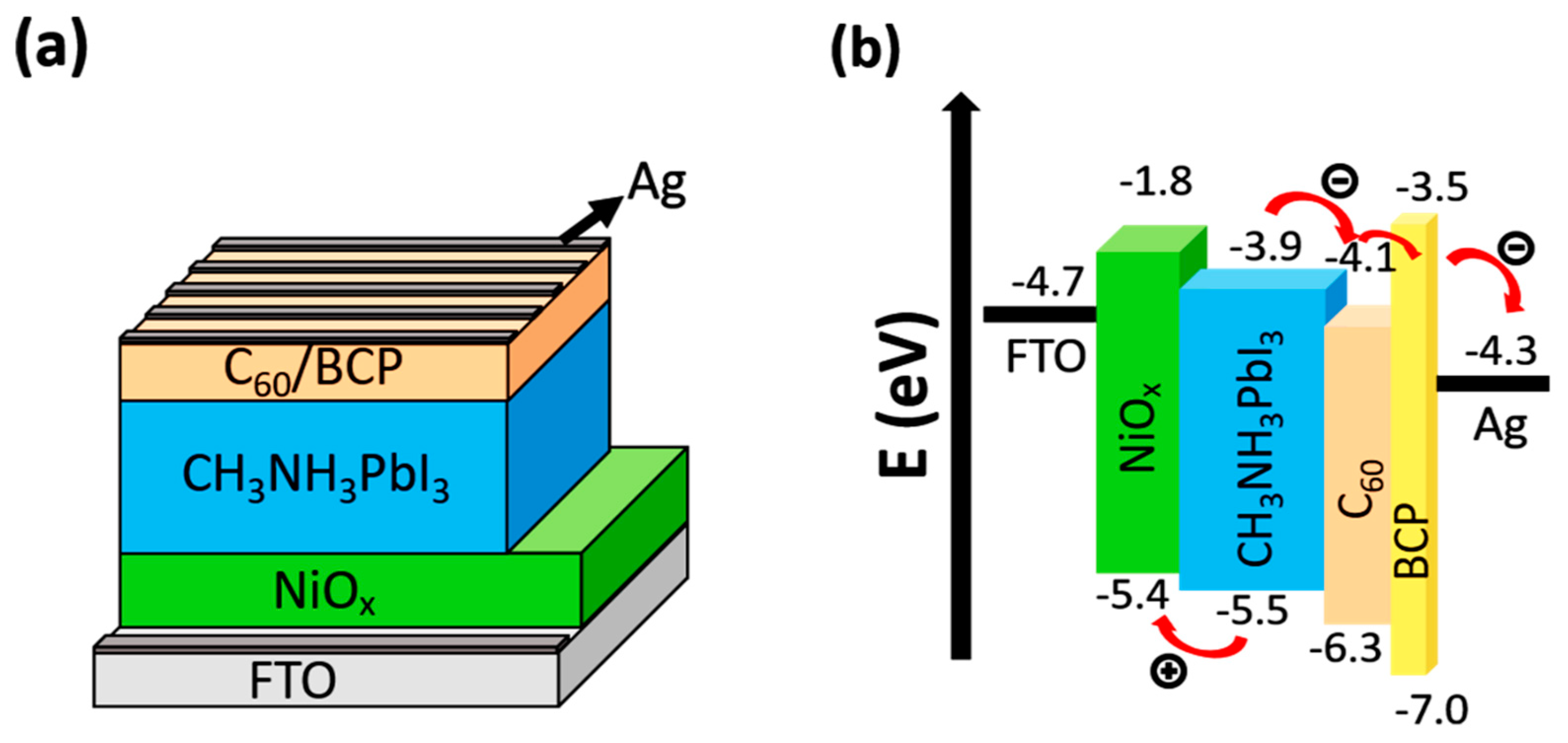
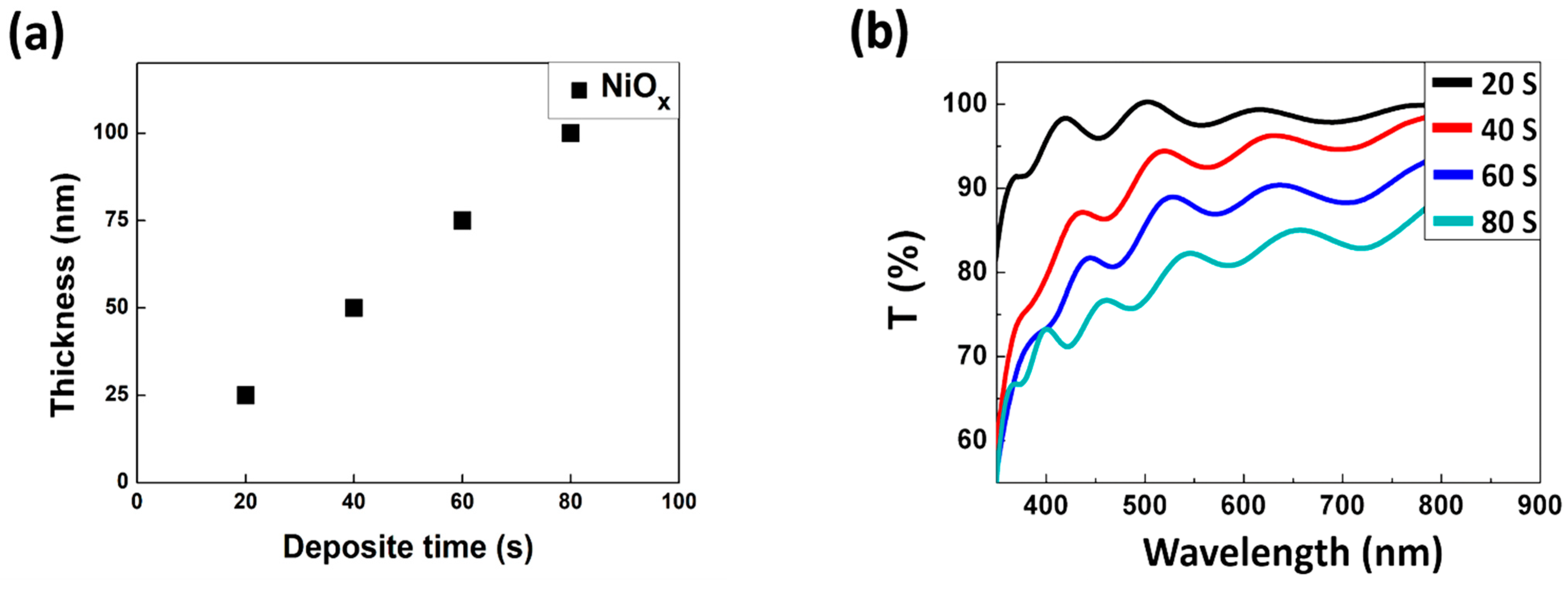
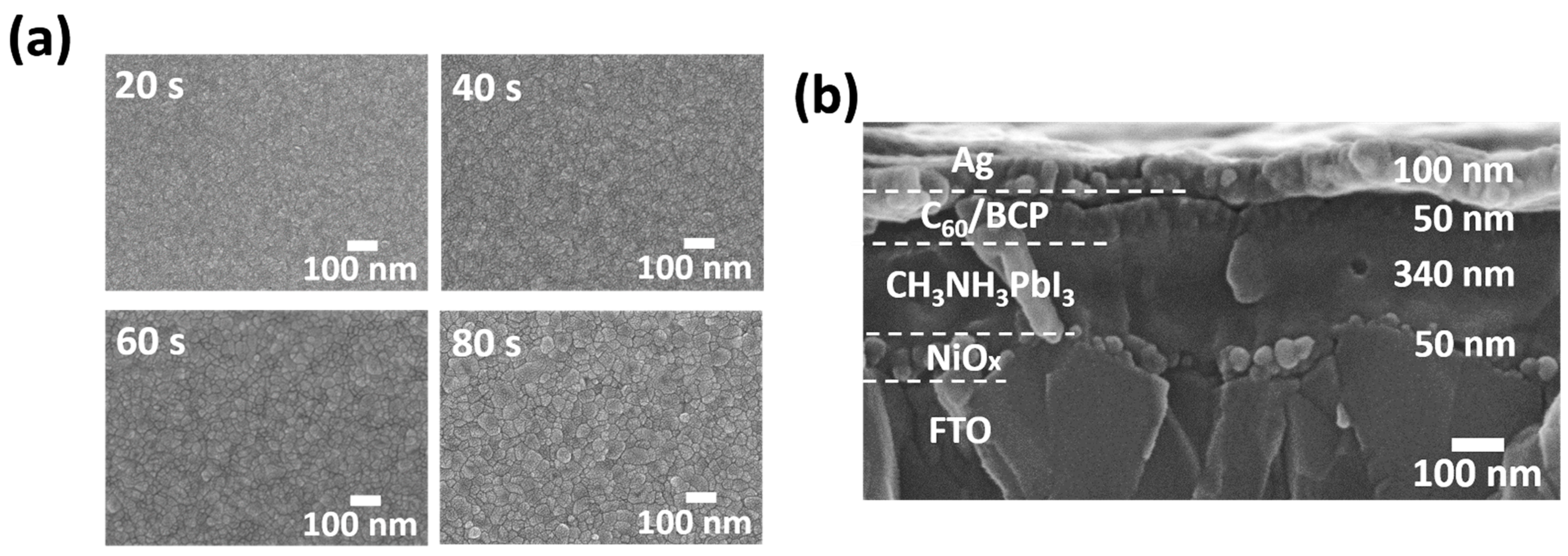
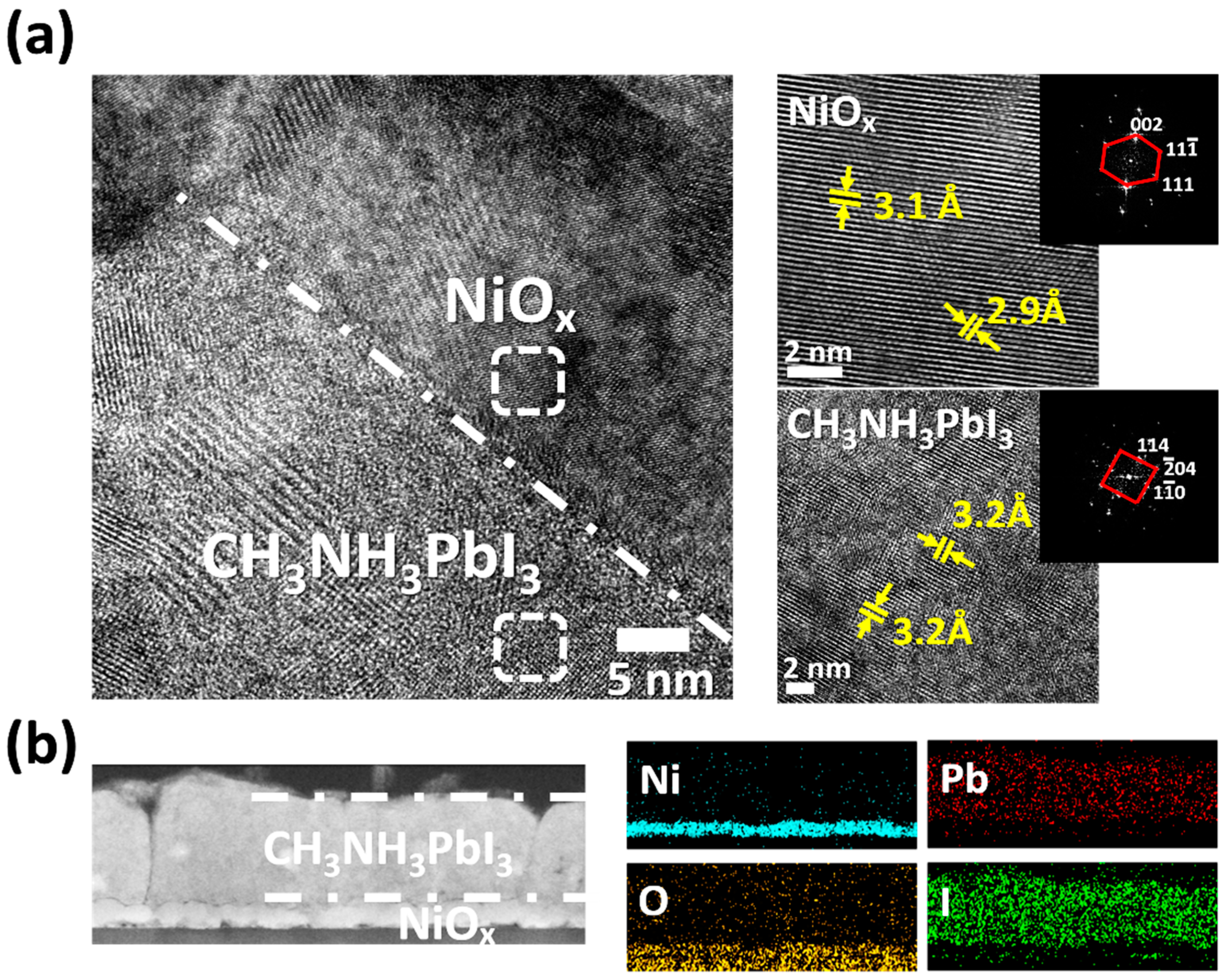
3. Results and Discussion

The work functions of FTO, NiOx, CH3NH3PbI3, C60, BCP, and Ag are also given in Figure 1b. When the light irradiates onto an absorber layer of the CH3NH3PbI3 film, the electrons were pumped from the valence band to the conduction band. Immediately, the electrons transport to the electron transport layer (ETL) of the n-type C60, while the holes transport to HTL of the NiOx layer. The C60 has a lower work function (−4.1 eV) which matches with the lowest unoccupied molecular orbital (LUMO) energy level of perovskite film (LUMO = −3.9 eV). The band structure of CH3NH3PbI3/C60 further accelerates the electron transport to the silver cathode (LUMO = −4.3 eV). To effectively guide holes, the work function of p-type NiOx (−5.4 eV) must be matched as much as possible with the Highest Molecular Orbital (HOMO) energy level of the FTO (HOMO = −4.7 eV). In order to avoid annihilation of a hole with an electron at the Ag electrode, the BCP is used to prevent hole transmission to the silver cathode, avoid electron and hole recombination at the interface while the p-type NiOx prevents the electron injection into the anode to affect the efficiency of the hole.
Figure 2a the NiOx films prepared for various deposition times: 20 s, 40 s, 60 s, and 80 s, respectively, were annealed at 500 °C for 1 h. The equivalent thicknesses of these films are 25 nm, 50 nm, 75 nm, and 100 nm, respectively. Figure 2b shows the UV-vis transmission spectra of the NiOx layer as a function of wavelength in the range (350~800 nm). All NiOx films have transmittance higher than 70% for wavelength longer than 400 nm. For 20 s and 40 s cases, the transmission even exceeds above 90%. Besides, the double layer and different pyramid period textures can increase transmission in the shorter wavelength. The high transmittance of NiOx films benefits the characters of being HTL due to the fact that the light can efficiently transport to FTO/NiOx/CH3NH3PbI3 for decreased quantum efficiency (QE) losses, which improve short-circuit current density (Jsc) and energy conversion efficiency [35,36,37].
X-ray diffraction (XRD) patterns of various NiOx layers are shown in Figure 3a. It is worth noting that the NiOx diffraction peaks can be observed when deposition time: 20 s, 40 s, 60 s, 80 s, respectively. The crystallinity of NiOx films becomes better with increase of deposition time. Figure 3a show the XRD patterns of NiOx films processed for various lengths of time with the θ–2θ (GIXRD) scan from 30° to 50°. Noted that only (111)NiOx, and (200)NiOx, at around 37° and 43°, are shown respectively (JCPDs card #73-1523). The CH3NH3PbI3 thin film was grown on NiOx substrate. There are several peaks (Figure 3b) at 14.08°, 20.8°, 23.51°, 24.55°, 28.4°, 31.86°, and 35.06°, respectively. These peaks correspond to the (110), (200), (211), (202), (220), (310), and (312), respectively, lattice planes of tetragonal CH3NH3PbI3 crystal. These peaks are in good agreement with those reported in earlier publications (JCPDs card #07-0235). XRD provides strong evidence for confirmation of the pristine crystal of NiOx and perovskite.
Figure 4a shows the surface microstructure and morphology of various thicknesses of NiOx HTLs processed at different deposition times. Obviously, all the NiOx HTLs uniformly cover the FTO surface without pinholes. We can observe the NiOx grain size increases as the sputter deposition time (20–80 s) increases. As a result, the resistivity of the NiOx films layer decreases since the area of grain boundary reduces. Here, the NiOx HTL is also known as the electron blocking layer, which can prevent intimate contact between the CH3NH3PbI3 and the FTO. Therefore, the NiOx layer can prohibit e-h charge recombination at the interface. A typical cross-sectional view for the inverted (p-i-n structure) perovskite solar cell NiOx/CH3NH3PbI3/C60/BCP/Ag is clearly shown in Figure 4b. All layers show uniform thickness without any pinhole. The thickness of each NiOx HTL layer is measured to be 50 nm, 340 nm, 50 nm, and 100 nm, respectively.
The HRTEM magnified image of NiOx (deposit = 40 s) and CH3NH3PbI3 film are given in Figure 5a. The crystal structures of NiOx and CH3NH3PbI3 phases can be confirmed from the Fourier transformed (FT) patterns of local atomic resolution images from the area enclosed in a white dotted line rectangular box (Figure 5a). From the FT patterns, we see NiOx and CH3NH3PbI3 are cubic structures and tetragonal structures, respectively. The elemental distribution of Ni (blue), Pb (red), O (yellow), and I (green) are presented in form of EDS maps of NiOx and CH3NH3PbI3 in Figure 5b.
The PL spectrum from FTO/NiOx/CH3NH3PbI3 can independently offer information of the structure and performance of cell PCE. In this study, CH3NH3PbI3 is coated on various thicknesses (25–100 nm) of NiOx HTL on bare glass. As a 633 nm laser is pumped onto the FTO/NiOx/CH3NH3PbI3 samples, an emission wavelength is expected to be detected at around 755 nm (Figure 6), which corresponds to a direct bandgap emission from first conduction band to first valence band of CH3NH3PbI3. The quenching of electron-hole pairs at the interface can be evaluated from relative PL intensity. Between the NiOx hole transport layer and the CH3NH3PbI3 layer. Since the laser enters from NiOx layer before CH3NH3PbI3 layer, the exciton quenching efficiency can be affected by the thickness of NiOx thin films. The relatively lower PL intensity represents higher quench efficiency [38,39] related to the fast hole mobility in NiOx layer such that the recombination of e-h in CH3NH3PbI3 layer is reduced. Compared to other deposition times, the NiOx film processed for 20 s (thickness = 25 nm) has lower efficient carrier extractions. Due to the work function mismatch with perovskite and the lower carrier mobility. Figure 6 shows the relative intensity of the PL signal has a positive dependence on the thickness of NiOx layer. It is obvious that NiOx film deposited for 40 s (thickness = 50 nm) shows the lowest PL intensity, which indicates that this NiOx layer collects holes with the highest efficiency, due to the fact hole mobility of NiOx films is thickness dependence. The higher PL signal may indicate that the electron-hole pair is relatively more difficult to be separated and collected at CH3NH3PbI3/NiOx interface. In addition, the work function measurement by UPS of the various thicknesses of NiOx films: 20 nm, 40 nm, 60 nm, and 80 nm are −5.1 eV, −5.4 eV, −5.3 eV, −5.2 eV, respectively. The NiOx films processed for 40 s (thickness = 50 nm) gives relative work function (HOMO = −5.4 eV) matches with that of the perovskite (HOMO = −5.5 eV). It is well-known, as the thickness increases in NiOx layer, the decrease in series resistance (Rs). The resistivity and mobility of the various thickness NiOx films (25–100 nm) are measured by the Hall Effect. The resistivity were 5.2 × 10⁻⁴ Ω/cm, 3.8 × 10⁻⁴ Ω/cm, 2.6 × 10⁻⁴ Ω/cm, and 1.4 × 10⁻⁴ Ω/cm, respectively. This is consistent with the grain size result shown in the SEM experiment (Figure 4a), and that the carrier mobilities were 0.27 cm2/Vs, 0.43 cm2/Vs, 0.51 cm2/Vs, and 0.54 cm2/Vs, respectively. It will be shown later this thickness dependent quenching effect will also be consistently evidenced in a systematical PCE test.
Based on the above results, inverted (p-i-n structure) perovskite devices are prepared. The photovoltaic performance (Figure 7a) for a device composed of NiOx/CH3NH3PbI3 perovskite film processed for 40 s (thickness = 50 nm) is shown. A typical Jsc-Voc curve and a table in Figure 7a shows the campion values of Voc = 1.05 V, Jsc = 23.89 mA/cm2, FF = 72.87%, and PCE = 18.3%, which gives an averaged PCE = 17.1% for 36 devices (under AM 1.5G illumination). The statistic PCE from 36 devices are given as an inset (red bar chart) with an active area of 0.16 cm2. A statistic table from the red bar chart shows averaged values and standard error (STD) of Voc, Jsc, FF, and efficiency of 36 devices. In the module (25 cm2), we demonstrate a perovskite device (active area 11.25 cm2) the parameters of the Voc = 4.55 V, short circuit current (Isc) = 40.81 mA, Jsc = 4.31 mA/cm2, and FF = 77% with an efficiency of 15.1% (Figure 7b). Figure 7c shows the consistent result that has been evidenced in the PL experiment (Figure 6). We observed that a 40 s deposit (thickness = 50 nm) is found to have the highest PCE since it had the best quench efficiency as suggested from the PL experiment. The efficiency of deposit NiOx films at 20 s (thickness = 25 nm), 40 s (thickness = 50 nm), 60 s (thickness = 75 nm), and 80 s (thickness = 100 nm) that 6.8%, 18.3%, 14.8%, 12.3%, respectively.
Compared the long-term perovskite device stability of CH3NH3PbI3 perovskite photovoltaic cells fabricated for the PEDOT:PSS and NiOx HTLs (thickness = 50 nm) (Figure 8). The durability test is carried out at RH = 40% and 25 °C. In general, the efficiency of perovskite solar cell devices with NiOx HTL is about 1.2 to 1.8 times superior to that with PEDOT:PSS. After 1200 h test, the CH3NH3PbI3 perovskite photovoltaic cells fabricated from NiOx and PEDOT:PSS decays 15.0% and 40.9% of their initial efficiencies, respectively.

4. Conclusions

In this research, our results strongly demonstrate a PVD processed with the high quality of NiOx (thickness = 50 nm) films for HTL gives a high optical transmittance (>90%), good chemical stability, lower resistivity, and HOMO match perovskite (CH3NH3PbI3) film layer. The performance of PSC explored here is an inverted (p-i-n structure) planar heterojunction perovskite solar cell with inorganic NiOx HTL and C60 ETL structure. The structural stacking is given as FTO/NiOx/CH3NH3PbI3/C60/BCP/Ag configuration. We produce about 36 devices of perovskite solar cells for repeatability tests. It was demonstrated PSC device with inorganic NiOx HTL (thickness = 50 nm) gives about 1.2–1.8 times better durability than with an organic PEDOT:PSS HTL and the device owns the highest PCE is approximately 18.30% with active areas of the device are 0.16 cm2 (under AM 1.5G illumination). In the module (25 cm2), we demonstrate a perovskite device (active area 11.25 cm2) with an efficiency of 15.1%.

Author Contributions

Conceptualization, C.-C.H. and C.-J.L.; Methodology, C.-C.H., S.-M.Y., K.-M.L. and C.-J.L.; Validation, C.-C.H., K.-M.L. and B.-Y.L.; Resources, S.-M.Y. and K.-M.L.; Writing—original draft preparation, C.-C.H.; Writing—review and editing, C.-C.H. and F.-R.C.; Supervision, F.-R.C. All authors have read and agreed to the published version of the manuscript.

Funding

This research was supported by the Ministry of Science and Technology, Taiwan (Grant Number: MOST 106-2218-E-182-005-MY2) and the Chang Gung Memorial Hospital, Linkou, Taiwan (CMRPD2G0301). FRC also would like to acknowledge the support from MOST-105-2221-E-007-023-MY3, MOST 104-2221-E-007-067-MY3, and the City University of Hong Kong under projects of project number 9360162 and 9380092.

Institutional Review Board Statement

Not applicable.

Informed Consent Statement

Not applicable.

Data Availability Statement

Not applicable.

Acknowledgments

We acknowledge the Ministry of Science and Technology, Taiwan (Grant Number: MOST 106-2218-E-182-005-MY2) and the Chang Gung Memorial Hospital, Linkou, Taiwan (CMRPD2G0301). FRC also would like to acknowledge the support from MOST-105-2221-E-007-023-MY3, MOST 104-2221-E-007-067-MY3, and the City University of Hong Kong under projects of project number 9360162 and 9380092.

Conflicts of Interest

The authors declare no conflict of interest.

References

  1. Min, H.; Lee, D.Y.; Kim, J.; Kim, G.; Lee, K.S.; Kim, J.; Paik, M.J.; Kim, Y.K.; Kim, K.S.; Kim, M.G.; et al. Perovskite solar cells with atomically coherent interlayers on SnO2 electrodes. Nature 2021, 598, 444–450. [Google Scholar] [CrossRef] [PubMed]
  2. Sadegh, F.; Akin, S.; Moghadam, M.; Keshavarzi, R.; Mirkhani, V.; Ruiz-Preciado, M.A.; Akman, E.; Zhang, H.; Amini, M.; Tangestaninejad, S.; et al. Copolymer-Templated Nickel Oxide for High-Efficiency Mesoscopic Perovskite Solar Cells in Inverted Architecture. Adv. Funct. Mater. 2021, 31, 2102237. [Google Scholar] [CrossRef]
  3. Akman, E.; Akin, S. Poly(N,N′-bis-4-butylphenyl-N,N′-bisphenyl)benzidine-Based Interfacial Passivation Strategy Promoting Efficiency and Operational Stability of Perovskite Solar Cells in Regular Architecture. Adv. Mater. 2021, 33, 2006087. [Google Scholar] [CrossRef] [PubMed]
  4. Akman, E.; Shalan, A.E.; Sadegh, F.; Akin, S. Moisture-Resistant FAPbI3 Perovskite Solar Cell with 22.25 % Power Conversion Efficiency through Pentafluorobenzyl Phosphonic Acid Passivation. ChemSusChem 2021, 14, 1176–1183. [Google Scholar] [CrossRef] [PubMed]
  5. Ozturk, T.; Akman, E.; Shalan, A.E.; Akin, S. Composition engineering of operationally stable CsPbI2Br perovskite solar cells with a record efficiency over 17%. Nano Energy 2021, 87, 106157. [Google Scholar] [CrossRef]
  6. Shalan, A.E.; Akman, E.; Sadegh, F.; Akin, S. Efficient and Stable Perovskite Solar Cells Enabled by Dicarboxylic Acid-Supported Perovskite Crystallization. J. Phys. Chem. Lett. 2021, 12, 997–1004. [Google Scholar] [CrossRef] [PubMed]
  7. Jung, H.S.; Park, N.G. Perovskite solar cells: From materials to devices. Small 2015, 11, 10–25. [Google Scholar] [CrossRef]
  8. Xing, G.; Mathews, N.; Sun, S.; Lim, S.S.; Lam, Y.M.; Grätzel, M.; Mhaisalkar, S.; Sum, T.C. Long-Range Balanced Electron- and Hole-Transport Lengths in Organic-Inorganic CH3NH3PbI3. Sci. Adv. 2013, 342, 344–347. [Google Scholar] [CrossRef]
  9. Bai, Y.; Yu, H.; Zhu, Z.; Jiang, K.; Zhang, T.; Zhao, N.; Yang, S.; Yan, H. High performance inverted structure perovskite solar cells based on a PCBM:polystyrene blend electron transport layer. J. Mater. Chem. A 2015, 3, 9098–9102. [Google Scholar] [CrossRef]
  10. Liang, P.W.; Chueh, C.C.; Williams, S.T.; Jen, A.Y. Roles of Fullerene-Based Interlayers in Enhancing the Performance of Organometal Perovskite Thin-Film Solar Cells. Adv. Energy Mater. 2015, 5, 1402321. [Google Scholar] [CrossRef]
  11. Yin, X.; Yao, X.; Luo, Q.; Dai, X.; Zhou, Y.; Zheng, Y.; Zhou, Y.; Luo, S.; Li, J.; Wang, N.; et al. High Efficiency Inverted Planar Perovskite Solar Cells with Solution-Processed NiOx Hole Contact. ACS Appl. Mater. Interfaces 2017, 9, 2439–2448. [Google Scholar] [CrossRef]
  12. Chang, S.H.; Lin, K.F.; Chiu, K.Y.; Tsai, C.L.; Cheng, H.M.; Yeh, S.C.; Wu, W.T.; Chen, W.N.; Chen, C.T.; Chen, S.H.; et al. Improving the efficiency of CH3NH3PbI3 based photovoltaics by tuning the work function of the PEDOT:PSS hole transport layer. Sol. Energy 2015, 122, 892–899. [Google Scholar] [CrossRef]
  13. Kim, S.K.; Seok, H.J.; Choi, D.H.; Nam, S.J.; Kim, S.C.; Kim, H.K. Comparison of NiOx thin film deposited by spin-coating or thermal ecaporation for application as a hole transport layer of perovskite solar cells. RSC Adv. 2020, 10, 43847–43852. [Google Scholar] [CrossRef]
  14. D’Amario, L.; Fohlinger, J.; Boschloo, G.; Hammarstrom, L. Unveiling hole trapping and surface dynamics of NiO nanoparticles. Chem. Sci. 2018, 9, 223–230. [Google Scholar] [CrossRef] [PubMed] [Green Version]
  15. Hossain, M.I.; Shahiduzzaman, M.; Ahmed, S.; Huqe, M.R.; Qarony, W.; Saleque, A.M.; Akhtaruzzaman, M.; Knipp, D.; Tsang, T.H.; Taima, T.; et al. Near field control for enhanced photovoltaic performance and photostability in perovskite solar cells. Nano Energy 2021, 89, 106388. [Google Scholar] [CrossRef]
  16. Hossain, M.I.; Shahiduzzaman, M.; Saleque, A.M.; Huqe, M.R.; Qarony, W.; Ahmed, S.; Akhtaruzzaman, M.; Knipp, D.; Tsang, Y.H.; Taima, T.; et al. Improved Nanophotonic Front Contact Design for High Performance Perovskite Single-Junction and Perovskite/Perovskite Tandem Solar Cells. Sol. RRL 2021, 5, 2100509. [Google Scholar] [CrossRef]
  17. Hossain, M.I.; Saleque, A.M.; Ahmed, S.; Saidjafarzoda, I.; Shahiduzzaman, M.; Qarony, W.; Knipp, D.; Biyikli, N.; Tsang, Y.H. Perovskite/perovskite planer tandem solar cells: A comprehensive guideline for reaching energy conversion efficiency beyond 30%. Nano Energy 2021, 79, 105400. [Google Scholar] [CrossRef]
  18. Muslih, W.Y.; Shahiduzzaman, M.; Akhtaruzzaman, M.; Hossain, M.I.; Wang, L.; Alkhammash, H.I.; Alharthi, S.S.; Nakano, M.; Karakawa, M.; Aminuzzaman, M. Reproducible perovskite solar cells using a simple solvent mediated sol−gel synthesized NiOx hole transport layer. Appl. Phys. 2022, 15, 015504. Appl. Phys. 2022, 15, 015504. [Google Scholar] [CrossRef]
  19. Hossain, M.I.; Hasan, A.K.M.; Qarony, W.; Shahiduzzaman, M.; Islam, M.A.; Ishikawa, Y.; Uraoka, Y.; Amin, N.; Knipp, D.; Akhtaruzzaman, A.; et al. Electrical and Optical Properties of Nickel- Oxide Films for Efficient Perovskite Solar Cells. Small Methods 2020, 4, 2000454. [Google Scholar] [CrossRef]
  20. Chen, W.; Liu, F.Z.; Feng, X.Y.; Djurišic´, A.; Chan, W.K.; He, Z.B. Cesium Doped NiOx as an Efficient Hole Extraction Layer for Inverted Planar Perovskite Solar Cells. Adv. Energy Mater. 2017, 7, 1700722. [Google Scholar] [CrossRef]
  21. Yan, W.; Ye, S.; Li, Y.; Sun, W.; Rao, H.; Liu, Z.; Bian, Z.; Huang, C. Hole-Transporting Materials in Inverted Planar Perovskite Solar Cells. Adv. Energy Mater. 2016, 6, 1600474. [Google Scholar] [CrossRef]
  22. Li, M.H.; Shen, P.S.; Wang, K.C.; Guo, T.F.; Chen, P. Inorganic p-type contact materials for perovskite-based solar cells. J. Mater. Chem. A 2015, 3, 9011–9019. [Google Scholar] [CrossRef]
  23. Chen, W.; Wu, Y.; Fan, J.; Djurišic´, A.; Liu, F.; Tam, H.W.; Ng, A.; Surya, C.; Chan, W.K.; Wang, D.; et al. Understanding the Doping Effect on NiO: Toward High-Performance Inverted Perovskite Solar Cells. Adv. Energy Mater. 2018, 8, 1703519. [Google Scholar] [CrossRef]
  24. Jeng, J.Y.; Chen, K.C.; Chiang, T.Y.; Lin, P.Y.; Tsai, T.D.; Chang, Y.C.; Guo, T.F.; Chen, P.; Wen, T.C.; Hsu, Y.J. Nickel Oxide Electrode Interlayer in CH3NH3PbI3 Perovskite/PCBM Planar-Heterojunction Hybrid Solar Cells. Adv. Mater. 2014, 26, 4107–4113. [Google Scholar] [CrossRef] [PubMed]
  25. Corani, A.; Li, M.H.; Shen, P.S.; Chen, P.; Guo, T.F.; Nahhas, A.E.; Zheng, K.; Yartsev, A.; Sundström, V.; Ponseca, C.S., Jr. Ultrafast Dynamics of Hole Injection and Recombination in Organometal Halide Perovskite Using Nickel Oxide as p-Type Contact Electrode. J. Phys. Chem. Lett. 2016, 7, 1096–1101. [Google Scholar] [CrossRef]
  26. Zhang, B.; Su, J.; Guo, X.; Zhou, L.; Lin, Z.; Feng, L.; Zhang, J.; Chang, J.; Hao, Y. NiO/Perovskite Heterojunction Contact Engineering for Highly Efficient and Stable Perovskite Solar Cells. Adv. Sci. 2020, 7, 1903044. [Google Scholar] [CrossRef] [Green Version]
  27. You, J.; Meng, L.; Song, T.B.; Guo, T.F.; Yang, Y.; Chang, W.H.; Hong, Z.; Chen, H.; Zhou, H.; Chen, Q.; et al. Improved air stability of perovskite solar cells via solution-processed metal oxide transport layers. Nat. Nanotechnol. 2016, 11, 75–81. [Google Scholar] [CrossRef]
  28. Yin, X.; Han, J.; Zhou, Y.; Gu, Y.; Tai, M.; Nan, H.; Zhou, Y.; Li, J.; Lin, H. Critical roles of potassium in charge-carrier balance and diffusion induced defect passivation for efficient inverted perovskite solar cells. J. Mater. Chem. A 2019, 7, 5666–5676. [Google Scholar] [CrossRef]
  29. Kim, H.; Lee, J.; Ok, S.; Choe, Y. Effects of pentacene-doped PEDOT: PSS as a hole-conducting layer on the performance characteristics of polymer photovoltaic cells. Nanoscale Res. Lett. 2012, 7, 5. [Google Scholar] [CrossRef] [Green Version]
  30. Ukoba, K.O.; Eloka-Eboka, A.E.; Inambao, F.L. Review of nanostructured NiO thin film deposition using the spray pyrolysis technique. Renew. Sustain. Energy Rev. 2018, 82, 2900–2915. [Google Scholar] [CrossRef]
  31. Qiu, Z.; Gong, H.; Zheng, G.; Yuan, S.; Zhang, H.; Zhu, X.; Zhou, H.; Cao, B. Enhanced physical properties of pulsed laser deposited NiO films via annealing and lithium doping for improving perovskite solar cell efficiency. J. Mater. Chem. C 2017, 5, 7084–7094. [Google Scholar] [CrossRef]
  32. Liu, Z.; Chang, J.; Lin, Z.; Zhou, L.; Yang, Z.; Chen, D.; Zhang, C.; Liu, S.; Hao, Y. High-Performance Planar Perovskite Solar Cells Using Low Temperature, Solution–Combustion-Based Nickel Oxide Hole Transporting Layer with Efficiency Exceeding 20%. Adv. Energy Mater. 2018, 8, 1703432. [Google Scholar] [CrossRef]
  33. Zhong, Y.; Suzuki, K.; Inoue, D.; Hashizume, D.; Izawa, S.; Hashimoto, K.; Koganezawa, T.; Tajima, K. Interface-induced crystallization and nanostructure formation of [6,6]-phenyl-C61-butyric acid methyl ester (PCBM) in polymer blend films and its application in photovoltaics. J. Mater. Chem. A 2016, 4, 3335–3341. [Google Scholar] [CrossRef]
  34. Hsu, C.C.; Yu, S.M.; Lee, K.M.; Lin, C.J.; Cheng, H.C.; Chen, F.R. Solid-state reaction process for high-quality organometallic halide perovskite thin film. Sol. Energy Mater Sol. Cells 2021, 227, 111014. [Google Scholar] [CrossRef]
  35. Qarony, W.; Hossain, M.I.; Jovanov, V.; Salleo, A.; Knipp, D. Influence of Perovskite Interface Morphology on the Photon Management in Perovskite/Silicon Tandem Solar Cells. ACS Appl. Mater. Interfaces 2020, 12, 15080–15086. [Google Scholar] [CrossRef]
  36. Hossain, M.I.; Hongsingthong, A.; Qarony, W.; Sichanugrist, P.; Konagai, M.; Salleo, A.; Knipp, D.; Tsang, Y.H. Optics of Perovskite Solar Cell Front Contacts. ACS Appl. Mater. Interfaces 2019, 11, 14693–14701. [Google Scholar] [CrossRef] [PubMed]
  37. Hossain, M.I.; Khan, H.A.; Kozawa, M.; Qarony, W.; Salleo, A.; Hardeberg, J.Y.; Fujiwara, H.; Tsang, Y.H.; Knipp, D. Perovskite Color Detectors: Approaching the Efficiency Limit. ACS Appl. Mater. Interfaces 2020, 12, 47831–47839. [Google Scholar] [CrossRef]
  38. Wheeler, S.; Deledalle, F.; Tokmoldin, N.; Kirchartz, T.; Nelson, J.; Durrant, J.R. Influence of Surface Recombination on Charge-Carrier Kinetics in Organic Bulk Heterojunction Solar Cells with Nickel Oxide Interlayers. Phys. Rev. Appl. 2015, 4, 024020. [Google Scholar] [CrossRef] [Green Version]
  39. Jin, Z.; Guo, Y.; Yuan, S.; Zhao, J.S.; Liang, X.M.; Qin, Y.; Zhang, J.P.; Ai, X.C. Modification of NiOx hole transport layer for acceleration of charge extraction in inverted perovskite solar cells. RSC Adv. 2020, 10, 12289–12296. [Google Scholar] [CrossRef] [Green Version]
Figure 1. The perovskite solar cell device: (a) Inverted (p-i-n structure) configuration; (b) the energy level diagram of the working principle.
Energies 15 00919 g001
Figure 2. NiOx films prepared to various deposit times: (a) from deposit times: 20 s, 40 s, 60 s, and 80 s, respectively, were annealed at 500 °C for 1 h. The equivalent thicknesses are 25 nm, 50 nm, 75 nm, and 100 nm, respectively; (b) transmittance vs. wavelength (350–900 nm) for various NiOx thin films.
Energies 15 00919 g002
Figure 3. The XRD diffraction patterns show: (a) NiOx hole transport layers deposited times for 20 s, 40 s, 60 s, and 80 s, respectively. All NiOx films were annealed at 500 °C for 1 h; (b) the XRD diffraction peak of a CH3NH3PbI3 perovskite film.
Energies 15 00919 g003
Figure 4. SEM images show surface morphology of various NiOx films on FTO substrate: (a) from top-view: disposition time: 20 s, 40 s, 60 s, and 80 s, respectively. These samples were annealed at 500 °C for 1 h; (b) cross-sectional view of a perovskite solar cell device with stacking sequence of FTO/NiOx/CH3NH3PbI3/C60/Bathocuproine (BCP)/Ag (both scale bars are 100 nm).
Energies 15 00919 g004
Figure 5. HRTEM image shows the crystal structure of NiOx/CH3NH3PbI3 films: (a) the NiOx/CH3NH3PbI3 films (scale bar is 5 nm). The dashed box areas of NiOx and CH3NH3PbI3 are shown as magnified views in the right-hand side (scale bar is 2 nm). Inset are FT patterns. The zone axis of NiOx (top): [110]cub, CH3NH3PbI3 (bottom): [221]tet. (b) EDS maps show the elemental distribution of Ni (blue), Pb (red), O (yellow), and I (green) of NiOx/CH3NH3PbI3.
Energies 15 00919 g005
Figure 6. PL spectrum for CH3NH3PbI3 perovskite film onto FTO/NiOx hole transport layers treated at various deposition times: 20 s, 40 s, 60 s, and 80 s, respectively.
Energies 15 00919 g006
Figure 7. Jsc-Voc curve and PCE related parameters of the perovskite device: (a) the statistic PCE from 36 devices are given as an inset (red bar chart). The average efficiency is 17.13%. A table shows averaged values and standard error of Voc, Jsc, FF, and efficiency of 36 devices under AM 1.5G illumination (active area 0.16 cm2).; (b) the perovskite device photograph for the module (25 cm2) with an efficiency of about 15.1% (active area 11.25 cm2). (c) shows the PCE efficiency of perovskite composed of NiOx thin films that annealed at 500 °C for 1 h with deposit times: 20 s, 40 s, 60 s, and 80 s, respectively.
Energies 15 00919 g007
Figure 8. The long-term perovskite device stability fabricated for the PEDOT:PSS (black line) and NiOx (red line) HTLs has been tested for 1200 h at 40% relative humidity (RH) and 25 °C.
Energies 15 00919 g008
Publisher’s Note: MDPI stays neutral with regard to jurisdictional claims in published maps and institutional affiliations.

