Article

Efficient n-i-p Monolithic Perovskite/Silicon Tandem Solar Cells with Tin Oxide via a Chemical Bath Deposition Method

1
Department of Materials Science and Engineering, Korea University, 145, Anam-ro, Seongbuk-gu, Seoul 02841, Korea
2
School of Civil, Environmental and Architectural Engineering, Korea University, 145, Anam-ro, Seongbuk-gu, Seoul 02841, Korea
3
KU-KIST Green School Graduate School of Energy and Environment, Korea University, 145, Anam-ro, Seongbuk-gu, Seoul 02841, Korea
*
Authors to whom correspondence should be addressed.
Energies 2021, 14(22), 7614; https://doi.org/10.3390/en14227614
Submission received: 14 October 2021 / Revised: 5 November 2021 / Accepted: 10 November 2021 / Published: 15 November 2021
(This article belongs to the Special Issue Advances in Photovoltaic Technologies)

Abstract

:
Tandem solar cells, based on perovskite and crystalline silicon absorbers, are promising candidates for commercial applications. Tin oxide (SnO2), applied via the spin-coating method, has been among the most used electron transfer layers in normal (n-i-p) perovskite/silicon tandem cells. SnO2 synthesized by chemical bath deposition (CBD) has not yet been applied in tandem devices. This method shows improved efficiency in perovskite single cells and allows for deposition over a larger area. Our study is the first to apply low-temperature processed SnO2 via CBD to a homojunction silicon solar cell without additional deposition of a recombination layer. By controlling the reaction time, a tandem efficiency of 16.9% was achieved. This study shows that tandem implementation is possible through the CBD method, and demonstrates the potential of this method in commercial application to textured silicon surfaces with large areas.

1. Introduction

Perovskite solar cells (PSCs) have come to be an attractive thin-film photovoltaic (PV) technology over the past decade, with power conversion efficiencies (PCEs) of up to 25.5% reported for single-junction devices [1] PSCs are characterized by a perovskite material sandwiched between an electron transport layer (ETL) and a hole transport layer (HTL). These PSCs can be divided into normal (n-i-p) and inverted (p-i-n) types according to the deposition order on the substrate. To date, the highest published efficiencies for single-junction PSCs have been reported for n-i-p architecture. Most high-efficiency perovskites in the n-i-p configuration use tin oxide (SnO2) as an ETL or a titanium dioxide (TiO2) bilayer composed of dense TiO2 and mesoporous TiO2 as the ETL [2,3]. Among them, SnO2 is particularly promising due to features such as a wide bandgap with light transmittance, high electron mobility, adequate chemical stability, and relative simplicity [4]. Unlike TiO2, it is widely used as an ETL in tandem devices to which PSCs are applied because it can be processed at a low temperature [4]. These SnO2 deposition technologies include spin-coating, chemical bath deposition (CBD), atomic layer deposition (ALD), and sputtering. Table 1 shows the results of the n-i-p PSCs reported so far when SnO2 was applied as the ETL using various deposition techniques. The Korea Research Institute of Chemical Technology (KRICT) reported the highest efficiency of PSCs at 25.2% power conversion efficiency by applying SnO2 as an ETL using the CBD method [2]. Jiang et al., reported a 23.6% efficiency of a PSC by applying SnO2 as an ETL using a spin-coating method [5].
CBD and spin coating have the common advantages of a simple process and an inexpensive technique, but CBD not only shows superiority in conformity and reproducibility compared with the spin-coating method, but also has scalability, enabling large-scale fabrication. Despite such high efficiency reports and advantages, monolithic perovskite/silicon tandem solar cells with CBD have not yet been reported, as shown in Table 2. This may be because the process is limited due to the synthetic atmosphere of SnO2 in the CBD method. The precursor solution for depositing SnO2 not only has sufficient solubility in an acidic environment, but also does not form an incomplete secondary phase in an environment with a pH close to 1. In general, indium tin oxide (ITO) has weaker acid resistance than fluorine-doped tin oxide (FTO), so an FTO substrate is used when manufacturing a perovskite single-junction solar cell using the CBD process. However, in order to fabricate tandem, because the top cell is manufactured after thinly depositing ITO as a recombination layer, the recombination layer may be damaged during the process in the acidic atmosphere.
In this study, we implemented the first n-i-p tandem by depositing SnO2 using the CBD method. In addition, we deposited the top cell directly on the bottom cell without depositing a recombination layer in order to exclude the cell degradation factor due to the acid-resistant atmosphere. First, we compared and analyzed the surface morphology according to the reaction time when SnO2 was formed on silicon with CBD. Then, we confirmed the interface between silicon and SnO2 by depositing SnO2 using spin coating and the CBD method on the silicon bottom cell and compared the morphology and reflectivity of SnO2 on silicon. From these results, we demonstrated for the first time the possibility of applying the CBD method to tandem.

2. Materials and Methods

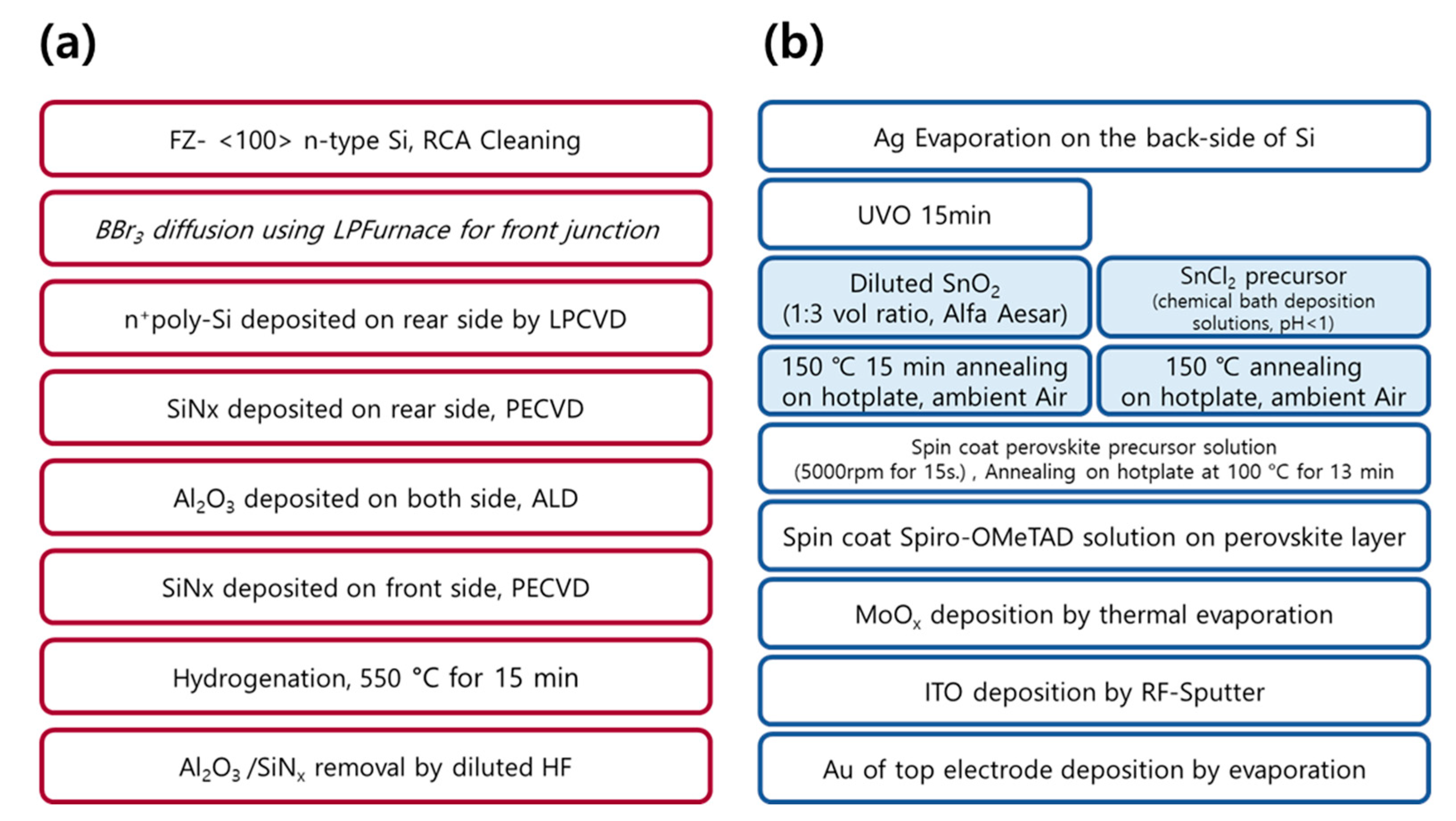
2.1. Fabrication of the Silicon Bottom Cell

N-doped FZ c-Si (silicon) wafers (15.24 cm × 15.24 cm (6 in.), (100) orientation, 270 µm, 3 Ω·cm) with both sides polished were used. The wafers were cleaned using the standard Radio Corporation of America (RCA) cleaning procedure. To form a front junction with a sheet resistance of 120–130 Ω/sq, a silicon oxide (SiOx) barrier was deposited on the back surface using plasma-enhanced chemical vapor deposition (PECVD). Additionally, a boron emitter was formed using boron tribromide (BBr3) in a liquid propane furnace at 985 °C. After removing the borosilicate glass and SiOx barrier using a dilute hydrofluoric acid (DHF) solution, we grew a thin SiOx (<2 nm) tunneling oxide structure on both surfaces by dipping the wafers into a hydrogen peroxide (H2O2) solution at 80 °C for 10 min. Subsequently, 300 nm phosphorous-doped polysilicon was deposited on the tunnel oxide using the low-pressure chemical vapor deposition equipment. To eliminate the SiOx/n+-poly-Si layer on the p+-emitter surface, a silicon nitride (SiNx) barrier was deposited on the back surface to protect the back-surface layer using PECVD. The sample was etched by dipping in a tetramethylammonium hydroxide (TMAH) solution and a DHF solution. As a result, the structure was p+-Si(emitter)/n-silicon(base)/SiOx/n+-poly-Si.
In addition, to improve the passivation quality, SiNx was deposited on the back surface using PECVD, and aluminum oxide (Al2O3) was deposited on both sides using atomic layer deposition (ALD). After depositing SiNx on the front surface, the sample was annealed at 550 °C for 15 min in a nitrogen (N2) atmosphere using rapid thermal processing (RTP). After hydrogenation, the SiNx/Al2O3 film was removed using DHF to deposit the perovskite top cell. Finally, silicon cell was cut to 2.5 cm × 2.5 cm to fabricate a tandem device. The process schematic for the bottom cell is shown in Figure 1a.

2.2. Fabrication of the Perovskite Top Cell

2.2.1. Materials

Cesium iodine (CsI), dimethylformamide (DMF), dimethyl sulfoxide (DMSO), thioglycolic acid and urea were procured from Sigma-Aldrich. The tin colloid precursor (tin (iv) oxide, 15% in H2O colloidal dispersion) was purchased from Alfa Aesar. The 2,2′,7,7′-tetrakis-(N,N-di-4-methoxyphenylamino)-9,9′-spirobifluorene (spiro-OMeTAD) was purchased from LumTec. The formamidinium iodide (FAI) and methylammonium bromide (MABr) was purchased from Greatcell solar. The lead iodine (PbI2) and lead bromide (PbBr2) was purchased from TCI. The ethyl ether was purchased from Duksan. The hydrogen chloride (HCl) was purchased from Samchun.

2.2.2. Methods

In this study, two different coating methods were used to fabricate the SnO2 layer. We employed spin-coating using a commercial water-based SnO2 nanoparticle solution. A UV-ozone (UVO) treatment was performed for 30 min to enhance the wettability of the silicone surface, and the solution was spin-coated on a silicon bottom cell at 3000 rpm for 30 s and annealed at 150 °C for 15 min. To fabricate the SnO2 layer using CBD, we prepared the following precursor solution: 5 g urea was dissolved in 400 mL deionized water, followed by the addition of 100 µL thioglycolic acid and 5 mL HCl. Finally, SnCl2∙2H2O was dissolved in the precursor solution at a concentration of 0.012 M and stirred for 3 h. The substrates were placed vertically in a glass bath filled with the final solution, and deposition was performed in a laboratory oven at 70 °C for 4, 8, and 24 h. The treated substrates were rinsed in a sonication bath of deionized water for 15 min, dried in a dry air stream, and annealed at 150 °C for 1 h.
To fabricate the perovskite layer, a 1.7 M Cs0.05FA0.8MA0.15PbI2.55Br0.45 precursor solution was prepared by dissolving CsI, FAI, PbI2, MABr, and PbBr2 in 0.72 mL of DMF and 0.18 mL of DMSO solution. The perovskite layer was spin-coated onto the SnO2 layer at 5000 rpm for 15 s. During spin-coating, 1 mL of ethyl ether was applied dropwise to the substrate to form the intermediate phase. The intermediate phase substrate was annealed at 100 °C for 13 min to crystallize into the perovskite phase. To fabricate the hole-transport layer, spiro-OMeTAD was dissolved in chlorobenzene (90.9 mg/mL). The fabrication method of the spiro-OMeTAD solution was prepared as described in our previous report [29] and was spin-coated onto the perovskite film at 2000 rpm for 30 s. A buffer layer of 10 nm MoOX was deposited on top of the spiro-OMeTAD, followed by 170 nm ITO deposited by magnetron sputtering at room temperature of about 20 °C. Layers of 100 nm Au were deposited on the ITO as the electrodes. Herein, the electrode was designed so that the active area is 0.1cm2 on the 2.5 cm × 2.5 cm substrate. Therefore, the active area of our tandem devices is 0.1 cm2. The process schematic for the bottom cell is shown in Figure 1b.

2.3. Characteristics

The J-V characteristics of the photovoltaic cells, including open-circuit voltage (Voc), short circuit current (Jsc), and fill factor (FF), were obtained using a Xe lamp solar simulator (WACOM WXS-155S10 class AAA) with a voltage setting time of 200 ms. The optical properties of the sample, such as its reflectance, were measured using an ultraviolet–visible (UV-Vis) spectroscopy (JASCO V-670 UV/Vis NIR spectrophotometer).

3. Results and Discussion

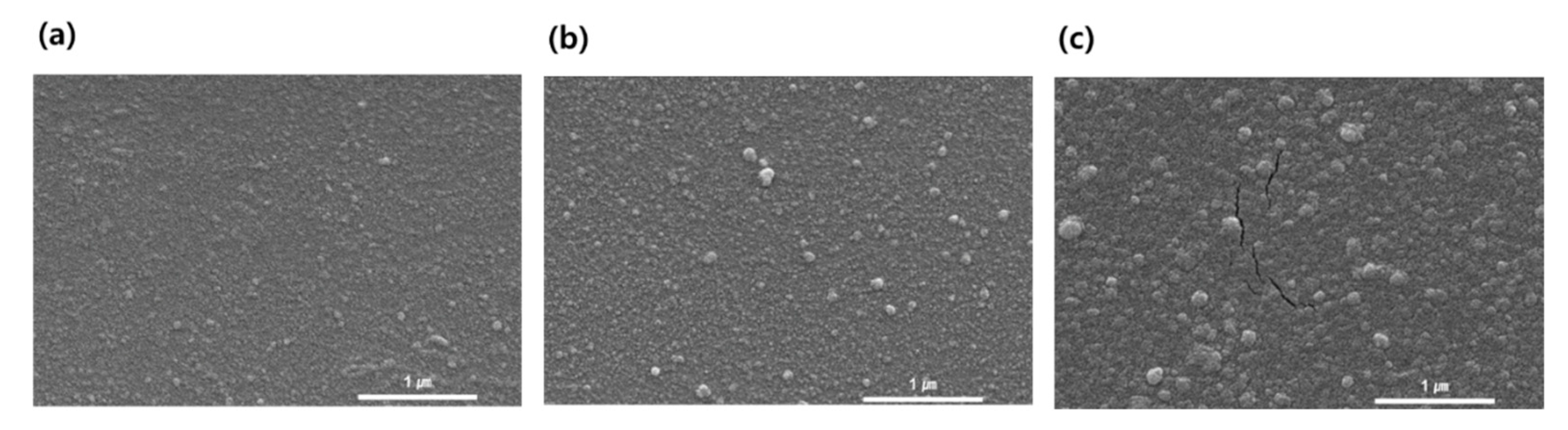
3.1. Comparison of Morphology According to Chemical Bath Deposition (CBD) Reaction Time

An experiment was conducted to confirm the surface shape according to the reaction time using the SnO2 formation reaction time as a variable. All silicon substrates polished on both sides were prepared by removing the native silicon oxide (SiOx) with dilute hydrofluoric acid (DHF) solution as recommended by Radio Corporation of America (RCA) cleaning. Then, the tin (Sn) precursor for tin oxide (SnO2) deposition was prepared using a tin (II) chloride dehydrate (SnCl2 2H2O) solution in a certain fraction of acid atmosphere. SnO2 is formed through the following reaction formula [30]:
Sn 2+ +2 OH Sn( OH )2  
Sn ( OH ) 2 SnO+ H 2 O 
SnO SnO 2  
In the tin chloride (SnCl2) aqueous solution, Sn exists as Sn2+ or Sn4+ ions. OH ions are attached to these ions to form an intermediate phase of Sn (OH)2 or Sn3(OH)4. Through this mesophase, it becomes SnO2 nucleation. Thus, the intermediate phase serves as a nucleation site for the formation of SnO2. Figure 2 shows the surface scanning electron microscopy (SEM) images of SnO2 formed on a silicon substrate through the reaction time. As shown in the SEM image, the size of the SnO2 particles on the silicon increased as the chemical bath deposition (CBD) time increased. As the reaction time increased, the number of nuclei with a critical size per unit volume increased, and the nucleation rate increased. However, as shown in Figure 2c, when the reaction time increased, not only the particle size increased, but also cracks occurred on the deposition surface due to the increase in the thickness of SnO2. These results show the trend according to the reaction time of SnO2 deposition and show that the desired morphology can be achieved.

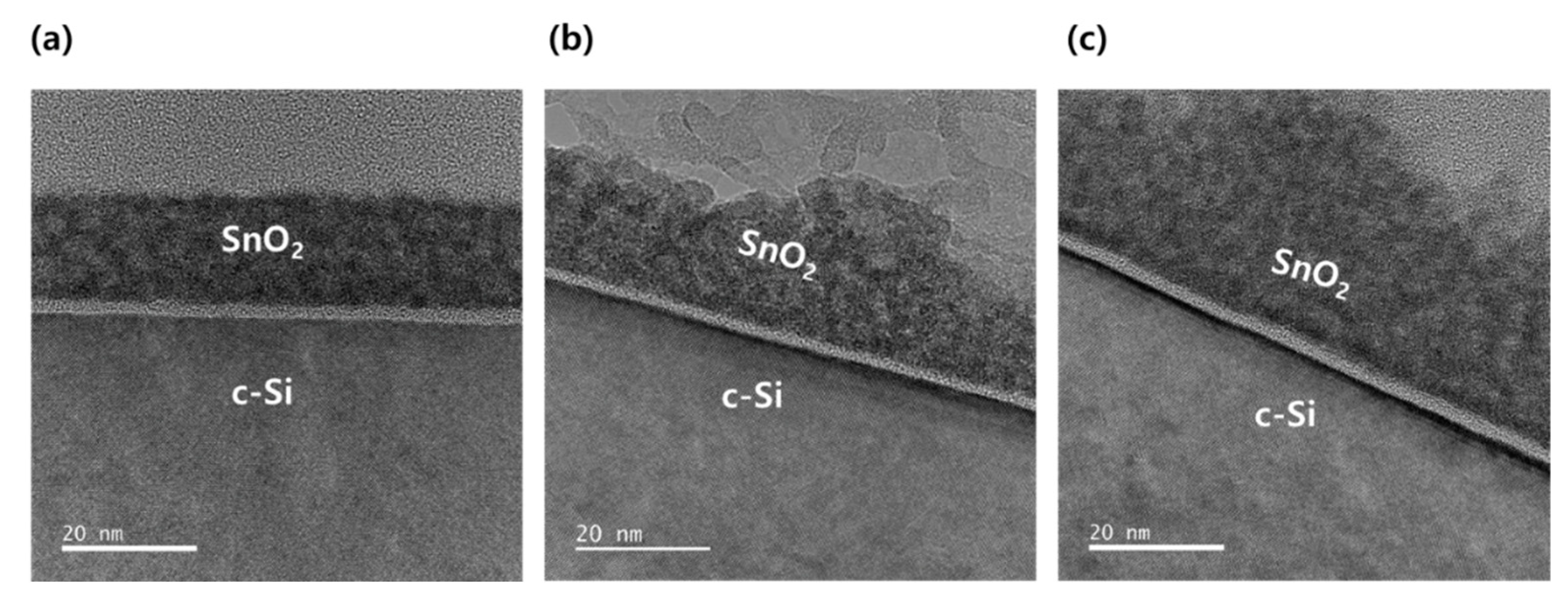
3.2. Interface between Si and SnO2 via TEM

Next, the characteristics at the interface with silicon during the SnO2 deposition were compared. Through the transmission electron microscopy (TEM) analysis, the SnO2/Si interface in the spin-coating and CBD method was compared, and the trend according to CBD time was confirmed. Figure 3a is the result of TEM analysis of the interface with silicon when SnO2 was deposited by spin coating, and it was confirmed that 1.85 nm of SiOx was present. However, in the case of deposition using the CBD method, SiOx was confirmed to be 1.27 nm for a 4 h reaction and 1.97 nm for an 8 h reaction. First, when the spin-coating method was applied, the thickness of SiOx was confirmed to be greater than that of CBD for 4 h, which seems to be due to the presence or absence of the UVO process. Because all silicon substrates used in this study were processed after cleaning, the silicon surface has hydrophobic properties. However, the SnO2 solution becomes hydrophilic because the precursor is diluted in deionized water (DI). Therefore, in the case of the spin-coating method, the UVO treatment must be performed on the silicon surface to form a uniform, high-coverage film. At this time, it seemed that SiOx was formed thicker than the CBD method because SnO2 was deposited in a state where SiOx was formed on the surface due to ozone. Second, the difference according to the reaction time of CBD was confirmed, and the thickness of SiOx at the interface increased as the reaction time increased. It is assumed that Sn (OH)2 is converted to SnO2 to generate H2O, and this H2O served as a source for SiOx growth. Therefore, it is concluded that as the reaction time increased, not only did the thickness of SnO2 but also the thickness of SiOx at the interface as silicon increased. In a tandem device, because vertical resistance is an important factor, it is crucial to design it so that tunneling through thin SiOx is possible. This result revealed the effect of the deposition method and time on SiOx thickness.

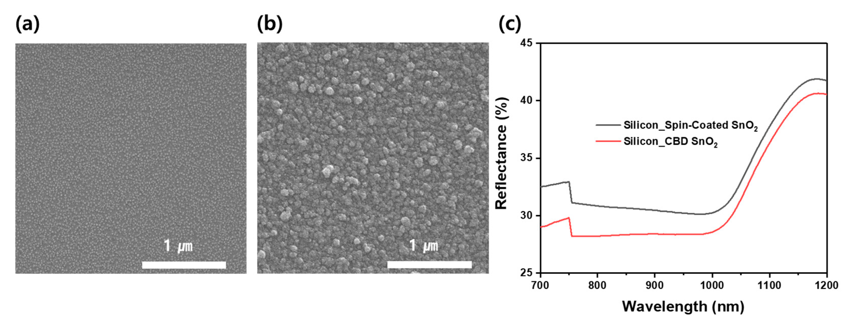
3.3. Comparison of Morphology and Reflectivity of CBD and Spin-Coated SnO2
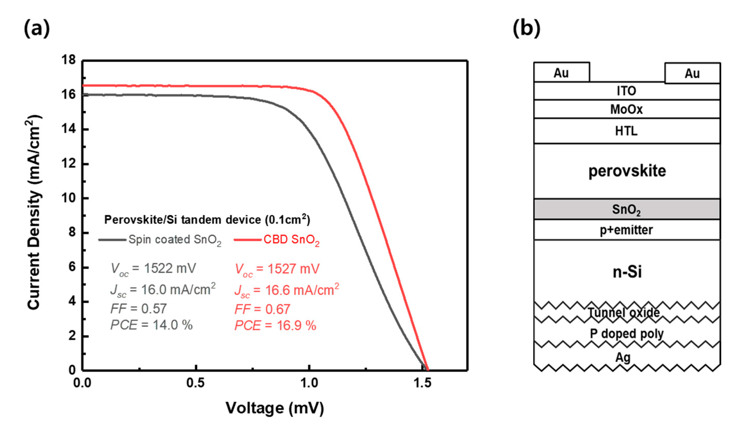
We conducted an SEM analysis of the morphology of the silicon surface following SnO2 deposition by spin-coating and CBD. Each surface was prepared with a thickness of approximately 30 nm (Figure 4a,b). With spin-coating, small SnO2 particles formed sparsely on the silicon substrate, and a low fractional coverage was observed. On the contrary, with CBD, larger SnO2 particles were formed on the silicon substrate, resulting in almost full coverage. This result indicates that the contact area between SnO2 and perovskite can vary depending on the method of fabrication. Since the increase in contact area helps to extract electrons from the perovskite light-absorbing layer and transfer them to the electrode, it can be inferred that the morphology of the SnO2 film affects the electrical behavior of the tandem device [31,32].
We compared reflectance values between surfaces to evaluate their optical properties (Figure 4c). In the wavelength range of 700–1200 nm of the bottom cell, the reflectivity of CBD-SnO2 was lower than that of spin-coated SnO2. Considering the incident direction of light, it can be determined that relatively more light is absorbed by the silicon solar cell through reduction in reflection in the long wavelength region. Therefore, we can determine that CBD SnO2 is more suitable for tandem solar cells than spin coating SnO2 based on the above analysis results.

3.4. Tandem Cell

To compare the photovoltaic properties of SnO2 with different deposition methods, SnO2-based monolithic perovskite/silicon was fabricated. Figure 5 shows the LIV measurement results of the tandem solar cells and the corresponding device structure. All parameters demonstrated relatively high values in the CBD-based tandem device. These results are consistent with our previous analysis results. In addition, in order to increase the reliability of our results, we additionally implemented a tandem device and created a histogram through it, which is shown in Scheme S1. Through the histogram result, it was confirmed that when CBD SnO2 was applied, it was possible to realize a tandem device with statistically higher efficiency than when the spin-coated SnO2 was applied. In particular, through the histogram, it was confirmed again that there is a performance improvement in the FF aspects. We judge that this improvement is the result of minimizing the formation of SiOx which can increase vertical resistance. The slope of the open circuit voltage point of the J-V curve shown in Figure 5a further supports this judgment. We can intuitively confirm that the slope at the open circuit voltage point is smaller when SnO2 by CBD is applied. This means that the series resistance of the tandem device is relatively small when CBD SnO2 is applied. This is consistent with the SiOx thickness trend confirmed through TEM analysis.
This is the first study to report a tandem solar cell with SnO2 applied using the CBD method. Our results support the potential of this process technology to replace spin-coating, which is not suitable for application to large surfaces or commercial use. It can also be applied to the rough surface of silicon owing to the characteristics of bath deposition. In future studies, we plan to fabricate monolithic perovskite/silicon tandem solar cells on a textured surface using commercially available silicon wafers grown by the Czochralski method.

4. Conclusions

Tin oxide, which can be realized by a low-temperature-solution process, has high potential as an electron transport layer of multi-junction solar cells as well as perovskite single-junction solar cells. Therefore, in this study, we compared the properties and functionality of silicon surfaces with SnO2 applied by nanoparticle spin-coating or CBD. Through this, we confirmed that the thickness of SiOx at the Si and SnO2 interface can be effectively minimized when SnO2 with an optimized chemical bath deposition reaction time is applied. This means that CBD SnO2 can suppress the formation of SiOx which can increase the vertical resistance of the tandem device. In addition, we confirmed that the reflectance in the wavelength range of 700–1200 nm can be minimized when CBD SnO2 is applied rather than SnO2 nanoparticle spin-coating. This means that when CBD SnO2 is applied, lighter in the long wavelength region absorbed by the silicon solar cell in the tandem structure which can be transmitted to the silicon solar cell.
These analysis results suggest that the optimized CBD SnO2 is electrically and optically more advantageous when applied to perovskite/silicon tandem solar cells. Therefore, we implemented a tandem solar cell in which CBD SnO2 is applied as an electron transport layer of the perovskite solar cell and at the same time acts as a bonding layer that monolithically connects the perovskite solar cell with the silicon solar cell. Through this approach, it was possible to demonstrate a perovskite/silicon tandem solar cell with improved performance in terms of Jsc and FF compared with when the nanoparticle SnO2 was applied. This attempt is the first study to apply SnO2 by CBD to n-i-p configuration monolithic perovskite/silicon tandem solar cells.

Supplementary Materials

The following are available online at https://www.mdpi.com/article/10.3390/en14227614/s1, Scheme S1: Histogram of monolithic perovskite/silicon solar cells with an active area of 0.1 cm2, in which SnO2 is fabricated by chemical bath deposition and spin-coating, respectively.

Author Contributions

J.H. and K.M.Y. contributed equally to this work. Conceptualization: J.H. and K.M.Y.; methodology: J.H., K.M.Y., and H.E.L.; formal analysis: J.H.; data verification: J.H. and K.M.Y.; writing—original draft preparation: J.H.; writing—review and editing: K.M.Y.; supervision: H.-S.L., D.K., J.H.N., and Y.K. All authors have read and agreed to the published version of the manuscript.

Funding

This research was supported by the Technology Development Program to Solve Climate Change of the National Research Foundation (NRF) funded by the Ministry of Science and ICT (NRF-2017M1A2A2087351) and the NRF grant funded by the Korean government (MSIT) (NRF-2020R1A2C1011815), and the NRF grant funded by the Korea government (MSIP) (NRF-2020R1A2C3009115). This work was also supported by Korea Institute of Planning and Evaluation for Technology in Food, Agriculture and Forestry (IPET) and Korea Smart Farm R&D Foundation (KosFarm) through Smart Farm Innovation Technology Development Program, funded by Ministry of Agriculture, Food and Rural Affairs (MAFRA) and Ministry of Science and ICT (MSIT), Rural Development Administration (RDA) (421036-03). And this work was also supported by the KU-KIST Graduate School Project.

Data Availability Statement

The data presented in this study are available within this article or Supplementary Material.

Acknowledgments

The authors are grateful to the reviewers and editors for their helpful comments and suggestions.

Conflicts of Interest

The authors declare no conflict of interest.

References

  1. Golden, C.O. Best Research-Cell Efficiency Chart; NRE: Golden, CO, USA, 2021. [Google Scholar]
  2. Yoo, J.J.; Seo, G.; Chua, M.R.; Park, T.G.; Lu, Y.; Rotermund, F.; Kim, Y.-K.; Moon, C.S.; Jeon, N.J.; Correa-Baena, J.-P. Efficient perovskite solar cells via improved carrier management. Nature 2021, 590, 587–593. [Google Scholar] [CrossRef]
  3. Jeong, J.; Kim, M.; Seo, J.; Lu, H.; Ahlawat, P.; Mishra, A.; Yang, Y.; Hope, M.A.; Eickemeyer, F.T.; Kim, M. Pseudo-halide anion engineering for α-FAPbI 3 perovskite solar cells. Nature 2021, 592, 381–385. [Google Scholar] [CrossRef]
  4. Altinkaya, C.; Aydin, E.; Ugur, E.; Isikgor, F.H.; Subbiah, A.S.; De Bastiani, M.; Liu, J.; Babayigit, A.; Allen, T.G.; Laquai, F.; et al. Tin oxide electron-selective layers for efficient, stable, and scalable perovskite solar cells. Adv. Mater. 2021, 33, 2005504. [Google Scholar] [CrossRef]
  5. Jiang, Q.; Zhao, Y.; Zhang, X.; Yang, X.; Chen, Y.; Chu, Z.; Ye, Q.; Li, X.; Yin, Z.; You, J. Surface passivation of perovskite film for efficient solar cells. Nat. Photon. 2019, 13, 460–466. [Google Scholar] [CrossRef]
  6. Turren-Cruz, S.-H.; Hagfeldt, A.; Saliba, M. Methylammonium-free, high-performance, and stable perovskite solar cells on a planar architecture. Science 2018, 362, 449–453. [Google Scholar] [CrossRef]
  7. Qiu, L.; Liu, Z.; Ono, L.K.; Jiang, Y.; Son, D.-Y.; Hawash, Z.; He, S.; Qi, Y. Scalable fabrication of stable high efficiency perovskite solar cells and modules utilizing room temperature sputtered SnO2 electron transport layer. Adv. Funct. Mater. 2019, 29, 1806779. [Google Scholar] [CrossRef]
  8. Zheng, J.H.; Lau, C.F.J.; Mehrvarz, H.; Ma, F.J.; Jiang, Y.J.; Deng, X.F.; Soeriyadi, A.; Kim, J.; Zhang, M.; Hu, L.; et al. Large area efficient interface layer free monolithic perovskite/homo-junction-silicon tandem solar cell with over 20% efficiency. Energy Environ. Sci. 2018, 11, 2432–2443. [Google Scholar] [CrossRef]
  9. Zheng, J.H.; Mehrvarz, H.; Ma, F.J.; Lau, C.F.J.; Green, M.A.; Huang, S.J.; Ho-Baillie, A.W.Y. 21.8% Efficient monolithic perovskite/homo-junction-silicon tandem solar cell on 16 cm2. ACS Energy Lett. 2018, 3, 2299–2300. [Google Scholar] [CrossRef]
  10. Zheng, J.H.; Mehrvarz, H.; Liao, C.; Bing, J.M.; Cui, X.; Li, Y.; Goncales, V.R.; Lau, C.F.J.; Lee, D.S.; Li, Y.; et al. Large-area 23%-efficient monolithic perovskite/homojunction-silicon tandem solar cell with enhanced uv stability using down-shifting material. ACS Energy Lett. 2019, 4, 2623–2631. [Google Scholar] [CrossRef]
  11. Albrecht, S.; Saliba, M.; Baena, J.P.C.; Lang, F.; Kegelmann, L.; Mews, M.; Steier, L.; Abate, A.; Rappich, J.; Korte, L.; et al. Monolithic perovskite/silicon-heterojunction tandem solar cells processed at low temperature. Energy Environ. Sci. 2016, 9, 81–88. [Google Scholar] [CrossRef]
  12. Fan, R.; Zhou, N.; Zhang, L.; Yang, R.; Meng, Y.; Li, L.; Guo, T.; Chen, Y.; Xu, Z.; Zheng, G. Toward full solution processed perovskite/Si monolithic tandem solar device with PCE exceeding 20%. Sol. RRL 2017, 1, 1700149. [Google Scholar] [CrossRef]
  13. Zhu, S.J.; Yao, X.; Ren, Q.S.; Zheng, C.C.; Li, S.Z.; Tong, Y.P.; Shi, B.; Guo, S.; Fan, L.; Ren, H.Z.; et al. Transparent electrode for monolithic perovskite/silicon-heterojunction two-terminal tandem solar cells. Nano 2018, 45, 280–286. [Google Scholar] [CrossRef]
  14. Zhu, S.J.; Hou, F.H.; Huang, W.; Yao, X.; Shi, B.; Ren, Q.S.; Chen, J.F.; Yan, L.L.; An, S.C.; Zhou, Z.X.; et al. Solvent Engineering to Balance Light Absorbance and Transmittance in Perovskite for Tandem Solar Cells. Sol. RRL 2018, 2, 1800176. [Google Scholar] [CrossRef]
  15. Hou, F.H.; Han, C.; Isabella, O.; Yan, L.L.; Shi, B.; Chen, J.F.; An, S.C.; Zhou, Z.X.; Huang, W.; Ren, H.Z.; et al. Inverted pyramidally-textured PDMS antireflective foils for perovskite/silicon tandem solar cells with flat top cell. Nano Energy 2019, 56, 234–240. [Google Scholar] [CrossRef]
  16. Hou, F.H.; Yan, L.L.; Shi, B.; Chen, J.F.; Zhu, S.J.; Ren, Q.S.; An, S.C.; Zhou, Z.X.; Ren, H.Z.; Wei, C.C.; et al. Monolithic Perovskite/Silicon-Heterojunction Tandem Solar Cells with Open-Circuit Voltage of over 1.8 V. ACS Appl. Energy Mater. 2019, 2, 243–249. [Google Scholar] [CrossRef]
  17. Hou, F.; Li, Y.; Yan, L.; Shi, B.; Ren, N.; Wang, P.; Zhang, D.; Ren, H.; Ding, Y.; Huang, Q. Control perovskite crystals vertical growth for obtaining high performance monolithic perovskite/silicon heterojunction tandem solar cells with VOC of 1.93 V. Sol. RRL 2021, 5, 2100357. [Google Scholar] [CrossRef]
  18. Chen, B.; Wang, P.; Li, R.; Ren, N.; Chen, Y.; Han, W.; Yan, L.; Huang, Q.; Zhang, D.; Zhao, Y. Composite electron transport layer for efficient NIP type monolithic perovskite/silicon tandem solar cells with high open-circuit voltage. J. Energy Chem. 2021. [Google Scholar] [CrossRef]
  19. Werner, J.; Weng, C.H.; Walter, A.; Fesquet, L.; Seif, J.P.; De Wolf, S.; Niesen, B.; Ballif, C. Efficient monolithic perovskite/silicon tandem solar cell with cell area > 1 cm2. J. Phys. Chem. Lett. 2016, 7, 161–166. [Google Scholar] [CrossRef]
  20. Werner, J.; Barraud, L.; Walter, A.; Brauninger, M.; Sahli, F.; Sacchetto, D.; Tetreault, N.; Paviet-Salomon, B.; Moon, S.J.; Allebe, C.; et al. Efficient near-infrared-transparent perovskite solar cells enabling direct comparison of 4-terminal and monolithic perovskite/silicon tandem cells. ACS Energy Lett. 2016, 1, 474–480. [Google Scholar] [CrossRef]
  21. Quiroz, C.O.R.; Spyropoulos, G.D.; Salvador, M.; Roch, L.M.; Berlinghof, M.; Perea, J.D.; Forberich, K.; Dion-Bertrand, L.I.; Schrenker, N.J.; Classen, A.; et al. Interface molecular engineering for laminated monolithic perovskite/silicon tandem solar cells with 80.4% fill factor. Adv. Funct. Mater. 2019, 29, 1901476. [Google Scholar] [CrossRef]
  22. Mailoa, J.P.; Bailie, C.D.; Johlin, E.C.; Hoke, E.T.; Akey, A.J.; Nguyen, W.H.; McGehee, M.D.; Buonassisi, T. A 2-terminal perovskite/silicon multijunction solar cell enabled by a silicon tunnel junction. Appl. Phys. Lett. 2015, 106, 121105. [Google Scholar] [CrossRef]
  23. Shen, H.P.; Omelchenko, S.T.; Jacobs, D.A.; Yalamanchili, S.; Wan, Y.M.; Yan, D.; Phang, P.; Duong, T.; Wu, Y.L.; Yin, Y.T.; et al. In situ recombination junction between p-Si and TiO2 enables high-efficiency monolithic perovskite/Si tandem cells. Sci. Adv. 2018, 4, eaau9711. [Google Scholar] [CrossRef]
  24. Bett, A.J.; Schulze, P.S.C.; Winkler, K.M.; Kabakli, O.S.; Ketterer, I.; Mundt, L.E.; Reichmuth, S.K.; Siefer, G.; Cojocaru, L.; Tutsch, L.; et al. Two-terminal perovskite silicon tandem solar cells with a high-bandgap perovskite absorber enabling voltages over 1.8 V. Prog. Photovolt. 2020, 28, 99–110. [Google Scholar] [CrossRef]
  25. Werner, J.; Walter, A.; Rucavado, E.; Moon, S.J.; Sacchetto, D.; Rienaecker, M.; Peibst, R.; Brendel, R.; Niquille, X.; De Wolf, S.; et al. Zinc tin oxide as high-temperature stable recombination layer for mesoscopic perovskite/silicon monolithic tandem solar cells. Appl. Phys. Lett. 2016, 109, 233902. [Google Scholar] [CrossRef]
  26. Wu, Y.L.; Yan, D.; Peng, J.; Duong, T.; Wan, Y.M.; Phang, S.P.; Shen, H.P.; Wu, N.D.; Barugkin, C.; Fu, X.; et al. Monolithic perovskite/silicon-homojunction tandem solar cell with over 22% efficiency. Energy Environ. Sci. 2017, 10, 2472–2479. [Google Scholar] [CrossRef]
  27. Sahli, F.; Kamino, B.A.; Werner, J.; Brauninger, M.; Paviet-Salomon, B.; Barraud, L.; Monnard, R.; Seif, J.P.; Tomasi, A.; Jeangros, Q.; et al. Improved optics in monolithic perovskite/silicon tandem solar cells with a nanocrystalline silicon recombination junction. Adv. Energy Mater. 2018, 8, 1701609. [Google Scholar] [CrossRef]
  28. Aydin, E.; Liu, J.; Ugur, E.; Azmi, R.; Harrison, G.T.; Hou, Y.; Chen, B.; Zhumagali, S.; De Bastiani, M.; Wang, M.; et al. Ligand-bridged charge extraction and enhanced quantum efficiency enable efficient n–i–p perovskite/silicon tandem solar cells. Energy Environ. Sci. 2021, 14, 4377–4390. [Google Scholar] [CrossRef]
  29. Jeon, N.J.; Na, H.; Jung, E.H.; Yang, T.-Y.; Lee, Y.G.; Kim, G.; Shin, H.-W.; Seok, S.I.; Lee, J.; Seo, J. A fluorene-terminated hole-transporting material for highly efficient and stable perovskite solar cells. Nat. Energy 2018, 3, 682–689. [Google Scholar] [CrossRef]
  30. Huang, L.; Sun, X.; Li, C.; Xu, J.; Xu, R.; Du, Y.; Ni, J.; Cai, H.; Li, J.; Hu, Z. UV-sintered low-temperature solution-processed SnO2 as robust electron transport layer for efficient planar heterojunction perovskite solar cells. ACS Appl. Mater. Interfaces 2017, 9, 21909–21920. [Google Scholar] [CrossRef]
  31. Lee, D.G.; Kim, M.; Kim, B.J.; Kim, D.H.; Lee, S.M.; Choi, M.; Lee, S.; Jung, H.S. Effect of TiO2 particle size and layer thickness on mesoscopic perovskite solar cells. Appl. Surf. Sci. 2019, 477, 131–136. [Google Scholar] [CrossRef]
  32. Kim, D.-S.; Park, G.S.; Kim, B.; Bae, S.; Park, S.Y.; Oh, H.-S.; Lee, U.; Ko, D.-H.; Kim, J.; Min, B.K. Achieving over 15% efficiency in solution-processed Cu (In, Ga)(S, Se) 2 thin-film solar cells via a heterogeneous-formation-induced benign p–n junction interface. ACS Appl. Mater. Interfaces 2021, 13, 13289–13300. [Google Scholar] [CrossRef]
Figure 1. Experimental procedure for fabricating monolithic perovskite/silicon tandem solar cells. (a) Preparation of the silicon bottom cell and (b) perovskite top cell.
Energies 14 07614 g001
Figure 2. Scanning electron microscopy (SEM) image of tin oxide (SnO2) morphologies deposited by chemical bath deposition (CBD) onto silicon substrates at (a) 4, (b) 8, and (c) 24 h.
Energies 14 07614 g002
Figure 3. Transmission electron microscopy (TEM) analysis of the Si/SnO2 interface under various conditions: (a) spin-coating tin oxide (SnO2) and (b) chemical bath deposition (CBD) at 4 h and (c) 8 h.
Energies 14 07614 g003
Figure 4. Scanning electron microscopy (SEM) images of SnO2 deposited onto silicon substrates using (a) spin-coating SnO2 and (b) chemical bath deposition (CBD) at 4 h. This sample was analyzed for reflectivity as well; (c) the reflectance curves of SnO2 in the wavelength range of 700–1200 nm.
Energies 14 07614 g004
Figure 5. Monolithic perovskite/silicon solar cells with an active area of 0.1 cm2. (a) J-V curves of tandem cells using SnO2 deposition by spin-coating and CBD. (b) Schematic of a perovskite/silicon tandem solar cell (not to scale).
Energies 14 07614 g005
Table 1. Various reported methods of normal (n-i-p) type single-junction perovskite solar cell (PSC) fabrication, using tin oxide (SnO2) electron transport layers (ETLs).
MethodDevice StructureVoc
(mV)
Jsc
(mA/cm2)
FF
(%)
Eff.
(%)
Stabilized
PCE (%)
Institute
CBDFTO/SnO2/perovskite/spiro/Au119425.0984.725.425.2KRICT [2]
Spin-coatingITO/SnO2/perovskite/PEAI/spiro/Au117924.981.423.5623.32ISCAS [5]
ALDFTO/SnO2/PCBM:PMMA/perovskite/PMMA/spiro/Au108025.0675.520.4420.35AMI, EPFL [6]
SputteringFTO/SnO2/perovskite/spiro/Au108023.779.020.219.8OIST [7]
CBD—chemical bath deposition; ALD—atomic layer deposition.
Table 2. Various materials and methods reported for n-i-p perovskite/silicon two-terminal tandem solar cell fabrication.
MaterialsMethodVoc
(mV)
Jsc
(mA/cm2)
FF
(%)
Eff.
(%)
Stabilized
PCE (%)
Active Area (cm2)Institute
SnO2Spin-coating167616.1782120.54UNSW [8]
165815.66817.617.116
174016.27821.921.816UNSW [9]
173216.58123.1234UNSW [10]
178514.07919.918.10.16HZB/EPFL [11]
170315.37920.618.00.03PKU [12]
171015.57118.8N/A0.13NKU [13]
178017.17422.8N/A0.13NKU [14]
175016.97421.9N/A0.13NKU [15]
183015.97020.4N/A0.13NKU [16]
193016.97424.2N/A0.86NKU [17]
192017.07825.4N/A0.5NKU [18]
PCBMSpin-coating169015.977.620.921.20.17EPFL [19]
170116.170.119.219.21.22
171816.473.020.620.51.43EPFL [20]
178014.780.4 210.15FAU [21]
Compact TiO2 + meso TiO2ALD158011.575 13.71MIT/Stanford [22]
170017.27923.222.91ANU [23]
176317.878.124.524.11
Evaporation183715.277.321.621.60.25Fraunhofer [24]
Sputter164315.36516.3161.43EPFL [25]
Spin-coating175017.67422.822.51.0ANU [26]
C60Evaporation175116.877.522.8220.25EPFL [27]
177716.574.421.821.21.43
176916.565.419.11812.96
C60 anchored a-NbOxSputter182819.575.927.1270.1KAUST [28]
PCBM—(6,6)-phenyl-C61 butyric acid methyl ester.
Publisher’s Note: MDPI stays neutral with regard to jurisdictional claims in published maps and institutional affiliations.

