Article

High-Power-Density DC–DC Converter Using a Fixed-Type Wireless Power Transmission Transformer with Ceramic Insulation Layer

1
Department of Electronics Engineering, Cheongju University, Cheongju 28503, Republic of Korea
2
Department of Electrical & Control Engineering, Cheongju University, Cheongju 28503, Republic of Korea
*
Author to whom correspondence should be addressed.
Energies 2022, 15(23), 9006; https://doi.org/10.3390/en15239006
Submission received: 27 October 2022 / Revised: 21 November 2022 / Accepted: 24 November 2022 / Published: 28 November 2022
(This article belongs to the Special Issue DC-DC Converters Technologies, Applications and Optimization)

Abstract

:
In this study, we propose the use of a short-distance and fixed-type wireless power transmission transformer via a half-bridge LLC resonant converter. A ceramic insulating layer was used instead of an air gap, meaning that the heat generated from the transformer core and the PCB winding was quickly transferred to the external metal case, with the ceramic insulating layer acting as a heat pipe. In order to stabilize the output voltage, we proposed the use of IR photo tunnel technology, and it was applied to two ceramic insulating layers so that the voltage error signal of the secondary output voltage could be transmitted as light to the primary side. As a result, it was possible to physically separate the primary and secondary sides of the power circuit centering on the ceramic insulating layer. The experiment was carried out with the input voltage of 400 V, the output voltage of 54 V, the maximum output power of 1 kW, and the switching frequency of 1.3 MHz or higher. As a result, the maximum operating frequency was 1.83 MHz, and the output voltage stability to the load was 0.49% or lower. The power density of the experimental circuit was 380 W / in 3 or higher, and the maximum power conversion efficiency was approximately 93% or higher.

1. Introduction

Recently, a rapid increase in the use of data by companies and individuals has been observed, and the storage and movement of data are becoming more important. The demand for high-speed communication devices that deliver massive data quickly is increasing. In miniaturization and high-efficiency technology, a DC–DC converter which supplies a stable DC voltage to communication devices is required to reduce the required installation space and maintenance costs. The miniaturization and high efficiency of the power supply are only possible when the device packaging technology is accompanied by power circuit design technology with low power loss. In particular, the power supply for communication devices operating in a limited space could be inefficient because the level of heat is increased if the internal power loss of the power system increases, and if the internal heat is not effectively handled, the maximum output power is limited. One of the indicators for the miniaturization of the power supply is power density, which represents the maximum output power per unit volume. In order to increase the power density, it is necessary to reduce the internal power loss, increase the power conversion efficiency, and simultaneously take comprehensive measures against heat dissipation [1,2,3,4]. A transformer is a typical element of a concentrated heat source in a power supply. It is technically easy to increase the switching frequency in order to increase the power density, and in particular, the size of the transformer core is inversely proportional to the operating switching frequency. On the other hand, the power dissipation of the transformer is proportional to the operating frequency. The loss of the magnetic material of the core and the loss of winding due to the skin effect are directly related to the operating frequency. Although most of the power loss of the transformer occurs as heat loss, in a miniaturized transformer, all of the windings are inside the core, making it difficult for the heat in the windings to dissipate outside of the transformer [5,6].
In general, a semiconductor device for power, which is essential in the composition of a power supply circuit, has switching loss and conduction loss due to high-frequency switching. The failure to effectively dissipate heat from the device due to power loss affects the lifespan of the power supply. The technical factors that hinder high power density in the power supply design stage are the increase in device heat generation and the limitation of the heat dissipation structure.
On the other hand, wireless power transmission technology is applied in various fields and enables power to be transmitted and received at a certain distance. In the case of magnetic induction, efficient wireless power transmission is possible at a relatively short distance, from several millimeters to several centimeters. The basic circuit method, which is suitable for wireless power transmission, should enable efficient power transmission even if the primary and secondary spaces of the transformer exist, and the LLC resonant converter is a basic circuit type [7,8,9,10]. A general wireless power transmission topology uses one or more L and C resonances centered on a transformer, and many studies have been actively conducted in the meantime. In this paper, an LLC resonant converter suitable for applications with a wide load range was used as the basic topology [11].
Figure 1 shows a basic circuit of a half-bridge LLC resonant converter. In the figure, the main switches of the converter are S 1 and S 2 , and the output voltage is controlled by changing the switching frequencies of the two switches. The primary side of the converter has a resonant capacitor, C R , a resonant inductor, L R , and a magnetizing inductor, L M ; the secondary side has a rectifying diode, an output voltage smoothing capacitor, C o , and a load resistor, R L . Figure 2 shows the ideal operating waveform of the LLC resonant converter operating in a steady-state. Figure 2a displays a case in which the switching frequency and resonant frequency are similar, and Figure 2b shows a case in which the switching frequency is smaller than the resonant frequency. From the top of the figure, the resonant inductor current, i L R , magnetizing inductor current, i L M , transformer secondary current, i S , and transformer primary voltage, v p , are depicted. As can be seen from the figure, although the switching frequency changes depending on the operating conditions, the waveforms of the resonant inductor current, L R , the primary current of the transformer, and the secondary current, i S , of the transformer maintain a shape similar to a sine wave. In LLC resonant converters, by adding an air gap to the transformer core, the resonant inductor, L R , and the magnetizing inductor, L M , can be replaced by parasitic inductors [12,13].
In this paper, a short-distance and fixed wireless power transmission transformer is proposed by modifying the transformer structure of a half-bridge LLC resonant converter. A ceramic insulating layer was used instead of an air gap, meaning the heat generated from the transformer and windings could be quickly transferred to the external metal case via the ceramic insulating layers, which acted as a heat pipe. In order to stabilize the output voltage, we proposed the use of infrared (IR) photo tunnel technology, which was applied to the multilayer ceramic insulation to transmit the voltage error signal of the secondary output voltage to the primary side, as light. As a result, it was possible to physically separate the primary and secondary power circuits with ceramic insulating layers as a center. The proposed technologies were applied to a power supply module for use in communication devices that require high power density, and an experimental circuit with an input voltage of 400 V, an output voltage of 54 V, and a maximum output of 1 kW was designed and constructed. We aimed to ensure that the height of the experimental power supply module was 10 mm or less, the power density was 380   W / in 3 or higher, and the maximum power conversion efficiency was 93% or higher.

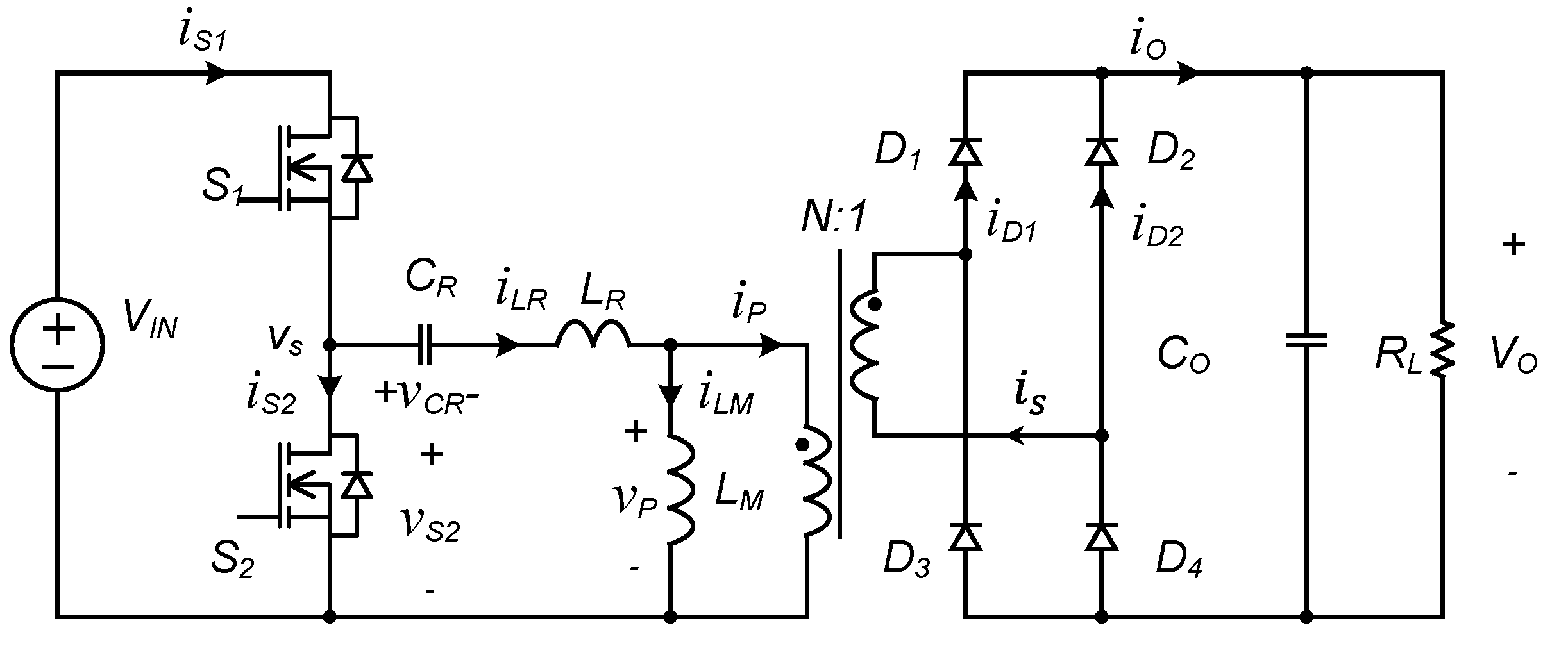
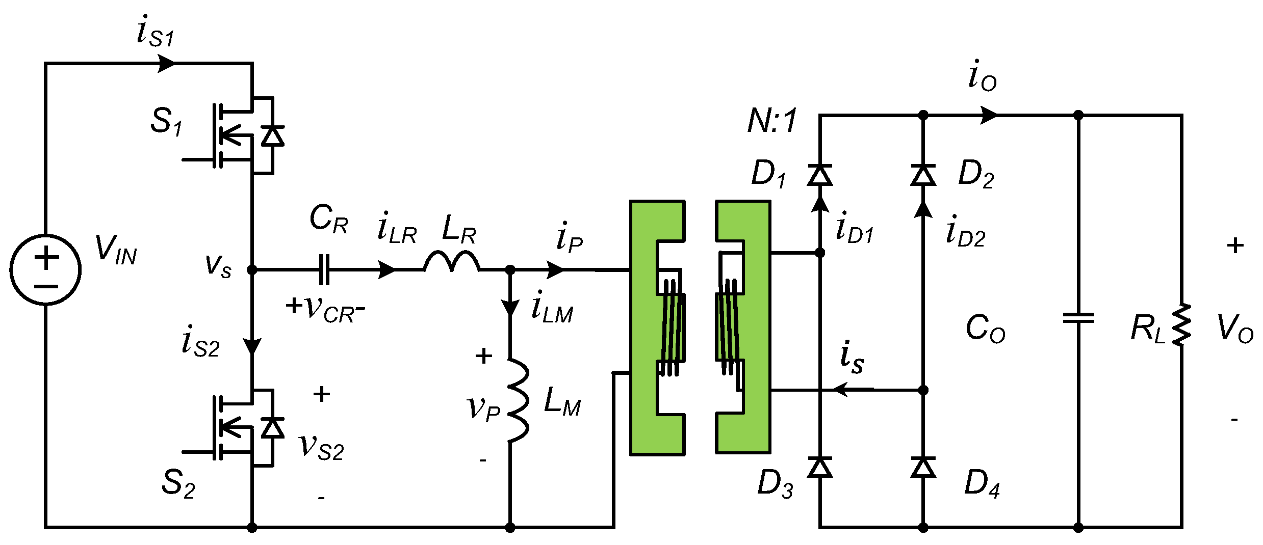
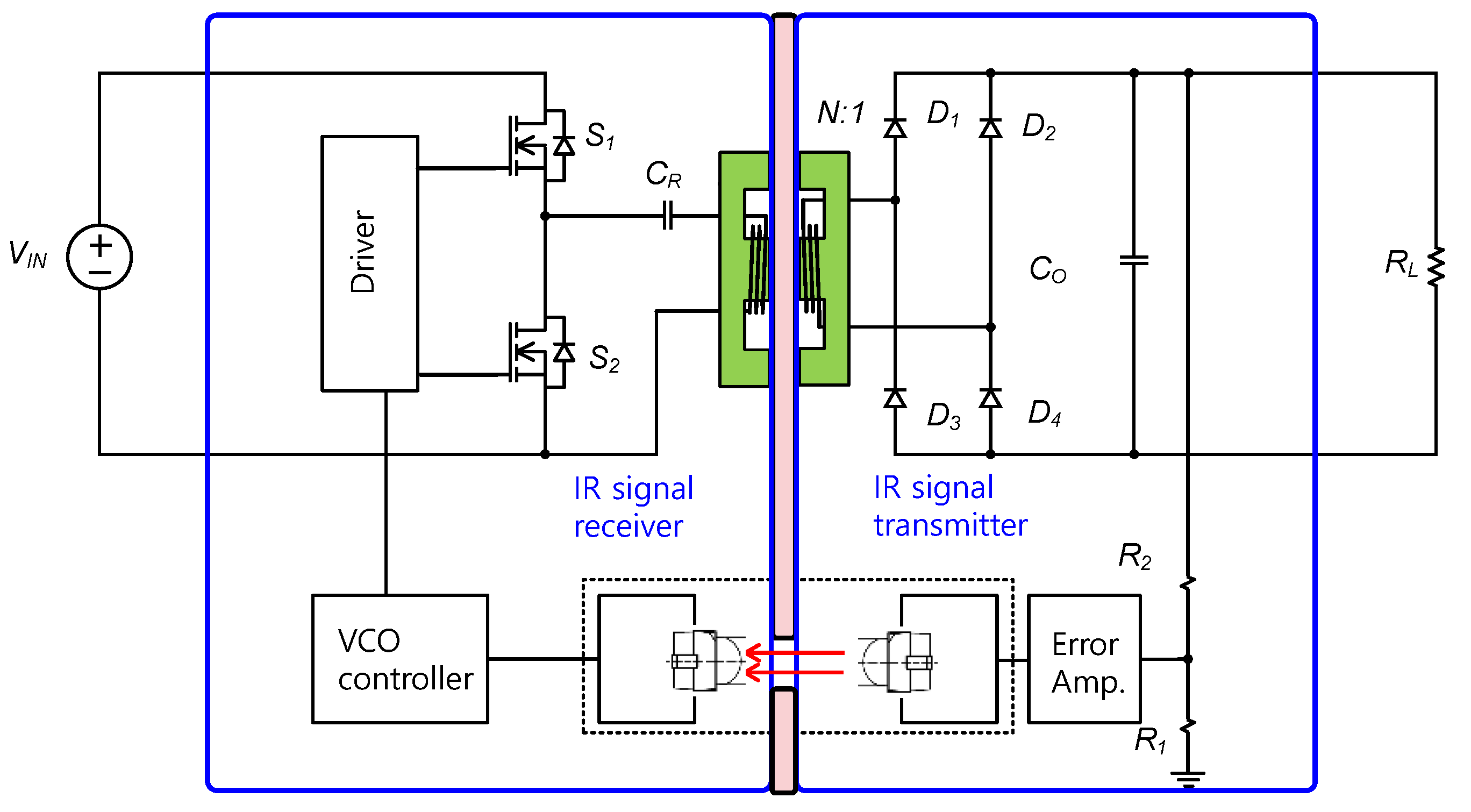
2. Wireless Power Transmission Converter

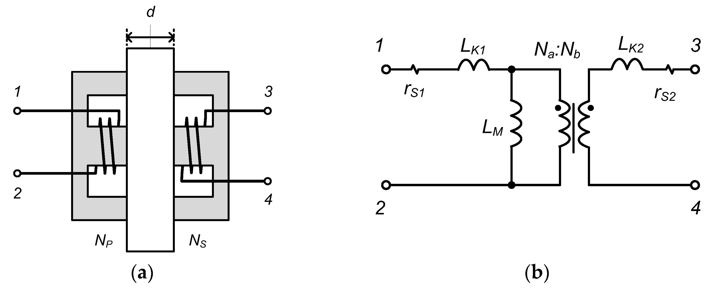
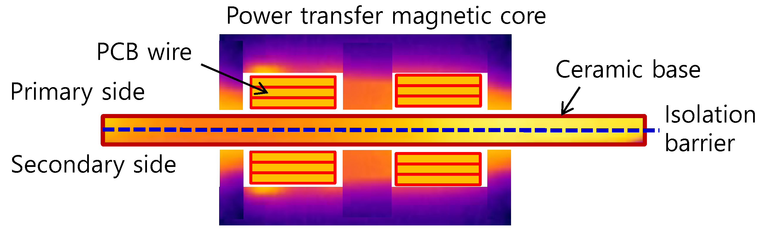
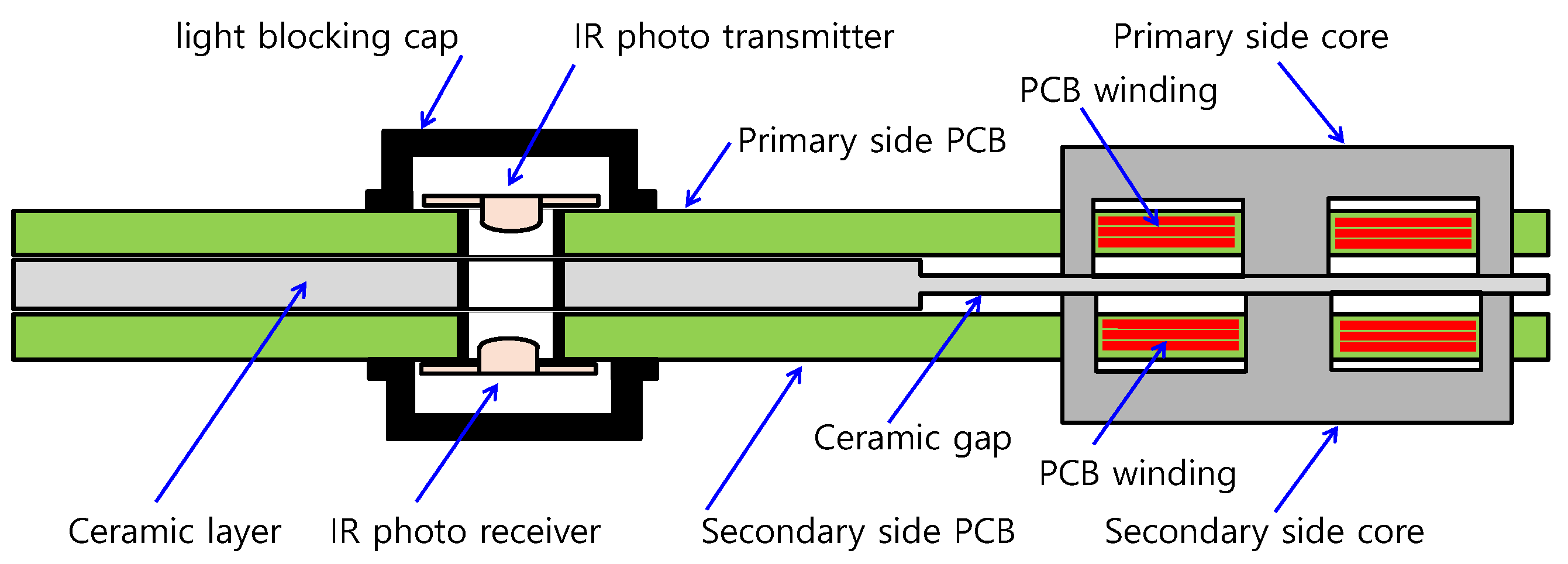
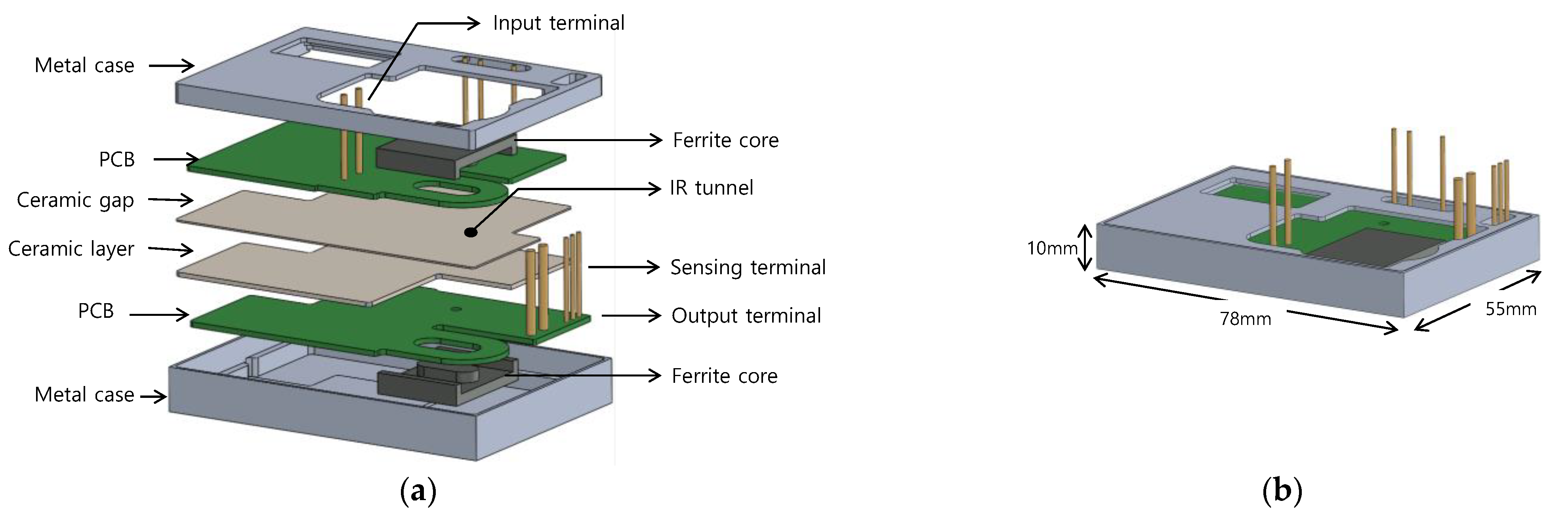
2.1. Wireless Power Transmission Transformer

Figure 3 shows the basic structure of a wireless power transmission transformer in which the core of the transformer is separated into primary and secondary sides in the basic circuit of a half-bridge LLC resonant converter, and a relatively large air gap is added. As shown in the figure, if the transformer core can be separated by a large air gap, the LLC resonant converter can physically separate the primary circuit and the secondary circuit. Figure 4 shows the transformer structure and equivalent circuit in a state in which the core of the transformer is separated by an insulator with no permeability. In Figure 4a, the transformer core is separated by an insulator of a certain thickness, d, and the primary-side core and the secondary-side core are attached to the insulator [14,15,16,17]. The equivalent circuit of the transformer is shown in Figure 4b. At this time, the equivalent circuit has the equivalent resistances, r s 1 and r s 2 , of the windings, the leakage inductances, L R , the magnetizing inductances, L M , and the turns ratios, N a and N b , of the ideal transformer. In general, the coupling ratio of the transformer varies according to the thickness of the insulator of the core. As a result, because the leakage inductance and magnetizing inductance of the transformer are varied, the leakage inductance can be determined by adjusting the appropriate insulator thickness. In general, if the leakage inductance and magnetizing inductance of the transformer are used as resonant elements of the LLC resonant converter, the two resonant inductors outside the transformer can be removed [18].
Figure 5 shows the basic circuit of an LLC resonant converter using the parasitic inductance of a transformer with an air gap added as a resonant inductor. In particular, if an insulator such as ceramic and a material with low magnetic permeability is used as an air gap between the primary and secondary cores of the transformer, a magnetic-induction-type wireless power transmission transformer structure is obtained. Figure 6 shows the thermal diffusion structure of a wireless power transmission transformer using ceramic sheets as an air gap. In general, the thermal conductivity of ceramics is approximately 20 W/mK or higher, and the insulation voltage is 12 kV/mm, which is very high, meaning ceramics have high heat dissipation and insulation properties [19,20,21]. In Figure 6, it can be seen that as the core and the windings of the transformer are attached to the ceramic insulating layers, the heat from the core and the windings passes through the ceramic insulating layers and has a structure similar to a heat pipe, where the heat can easily diffuse outside.

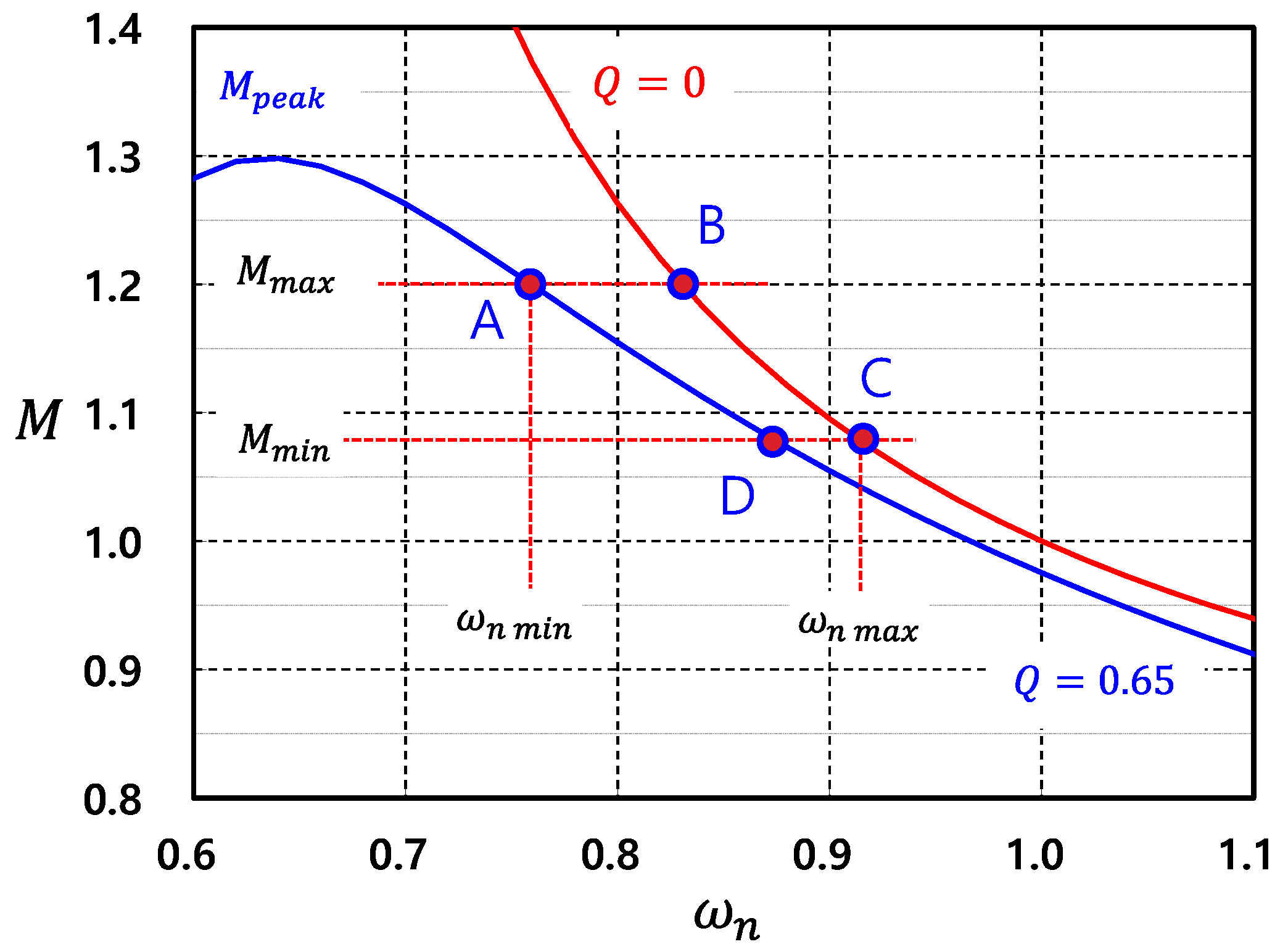
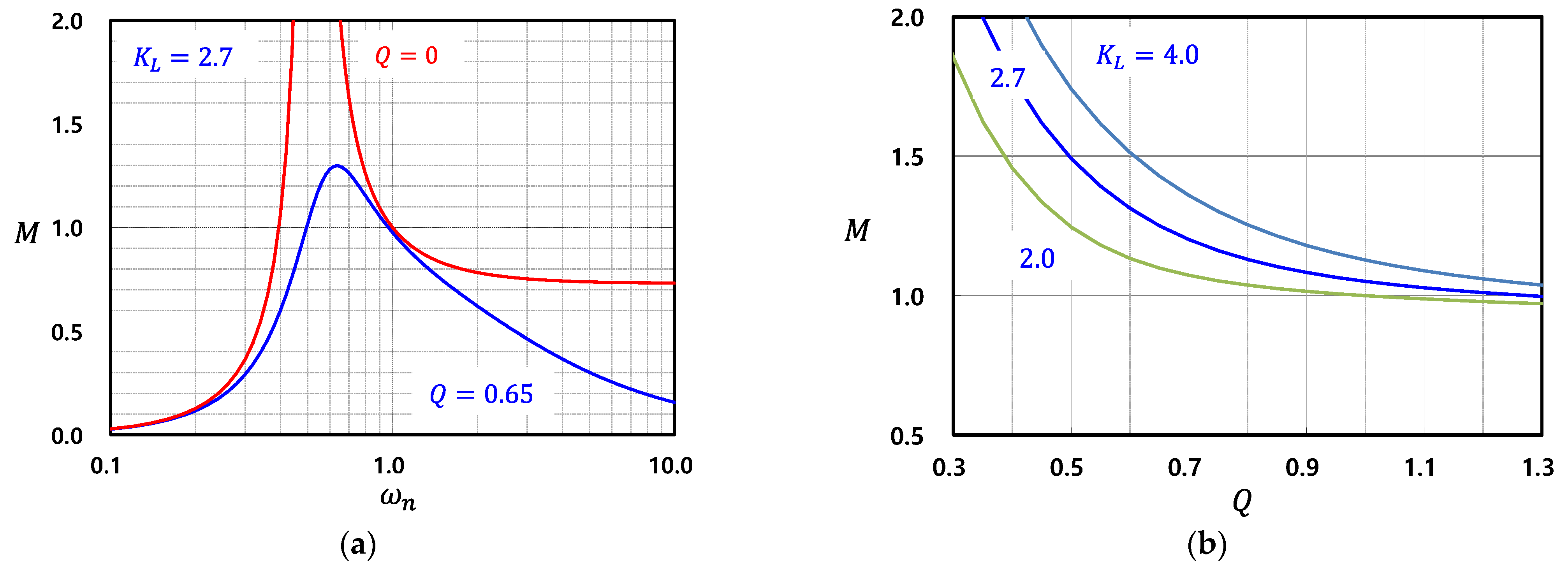
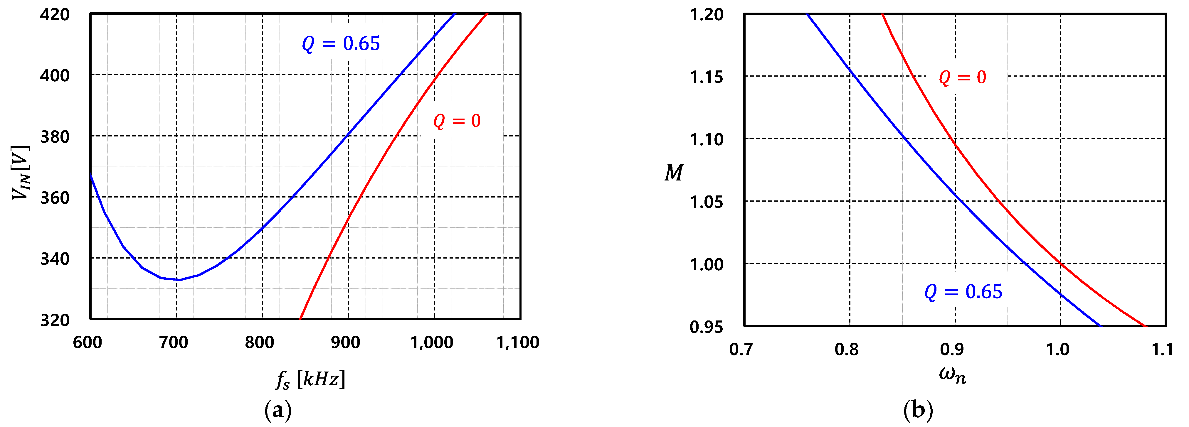
2.2. DC Voltage Gain in Steady-State

As the LLC resonant converter with the wireless power transmission transformer shown in Figure 5 has the same equivalent circuit structure as the conventional LLC resonant converter, the steady-state characteristics are also the same. Many studies have been carried out regarding the input and output DC voltage gain of LLC resonant converters, but in these studies, the voltage gain considering the internal loss resistance was not applied. In this paper, the optimal design was achieved using the steady-state characteristic equation which considered the internal loss equivalent resistance [22,23,24]. First, the steady-state input and output voltage gain equation, considering the internal loss resistance, r, of an LLC resonant converter, can be obtained as shown in Equation (1). Assuming that the internal equivalent resistance, R K , is 0 in the equation, it is the same as the conventional DC voltage gain result. It is known that the resonant element and transformer design results using Equation (1) are relatively accurate compared to the existing lossless design results. In this paper, the main resonant elements and transformer were designed using the steady-state result equation considering the internal equivalent resistance [25].
M = 2 N V o V I N = 1 + ( R K ω n K L ) 2 ( 2 Q R K + 1 ) 2 [ 1 + 1 K L ( 1 1 ω n 2 ) ] 2 + ( 2 R K ω n Q K L + 1 ω n ω n ) 2 Q 2
where Z o is a characteristic impedance; L M is a magnetizing inductance; L R is a resonant inductance; K L is an inductance ratio; C R is a resonant capacitor; ω o is a resonant angular frequency; ω n is an angular normalized frequency; ω f is an angular switching frequency.
R A C = 8 N 2 π 2 R L
K L = L M L R
Z o = L R C R
ω o = 1 L R   C R
ω n = ω f ω o
Q = Z o R A C
R K = r Z o

3. Design of Wireless Power Transmission (WPT) Converter

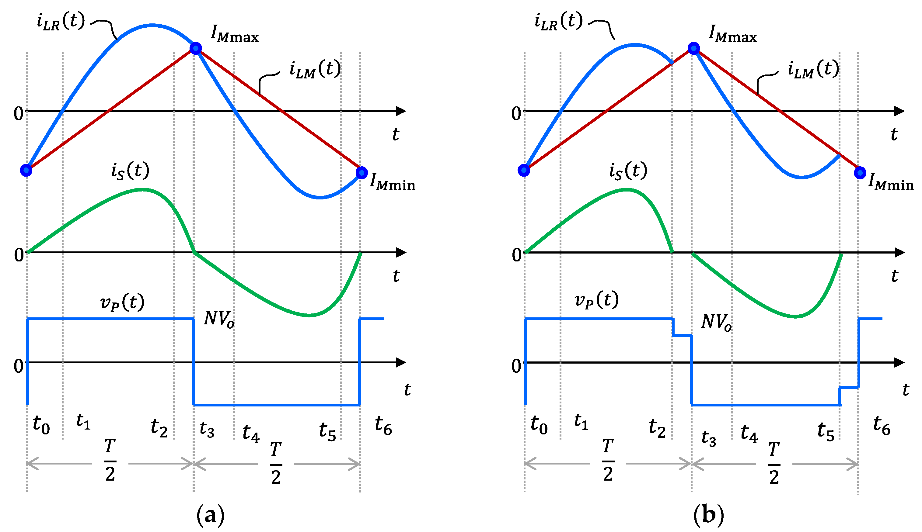
3.1. Optimal Design Process

For the design of the LLC resonant converter with the wireless power transmission transformer shown in Figure 5, the electrical specifications shown in Table 1 were established. The power supply module in a communication device uses a DC voltage of approximately 390 V (which is a rectified AC voltage) as an input, and the output voltage is 54 V to charge the battery. The maximum output power is approximately 1 kW, and in order to reduce the size of the transformer and capacitor, the switching frequency is operated at 1 MHz or more. The inductance ratio, K L , is an important factor in the design process of the LLC resonant converter. In this paper, the target value of the inductance ratio, K L , was approximately 3, considering the characteristics of a transformer with a ceramic insulating layer.
The turns ratio of the transformer was calculated as in Equation (9), and in this design, the secondary winding of the transformer was determined as four turns because the minimum natural number was set. The equivalent AC resistance of the converter was the same as Equation (10), and the maximum and minimum voltage gain according to the input voltage range were as shown in Equations (11) and (12). Figure 7 shows the operating area that meets the electrical specifications of the converter. The graph in Figure 7 can be expressed by the normalized angular velocity and voltage gain equations in Equation (1). In the figure, the maximum value of Q which satisfies the range of the maximum and minimum input/output voltage ratio was 0.7, but, in consideration of the component errors and as shown in Equation (13) it was set to 0.63, which was 90% of the ratio [26,27,28]. The characteristic impedance was the same as that in Equation (14), and using this result, the main resonant element was as shown in Equations (15)–(17). The operating area of the LLC converter in Figure 7 was inside the rectangle connecting points A–B–C–D, and the range of normalized angular velocity can be seen in the figure. Figure 8 is a graph of the frequency characteristics of voltage gain. Figure 8a shows the frequency characteristics for the maximum and minimum loads, and Figure 8b is a graph of the inductance ratio and voltage gain. The inductance ratio, K L , may have deviated from the original design range due to component errors during the transformer manufacturing process. From Figure 8b, it can be seen that the voltage gain changed according to the inductance ratio in three cases [29,30,31].
Figure 9 is a graph showing the change in the switching frequency according to the load current range using the steady-state characteristic expression, Equation (1). At this time, the output voltage was fixed at 54 V. Figure 9a shows the relationship between the switching frequency and the input voltage as a graph. Figure 9b shows the normalized angular velocity, ω n , and the voltage gain, M, as a graph. The figure shows the turns ratio of the transformer, including the resonant element, which was properly designed within the electrical specification range of the LLC resonant converter to which the wireless power transmission transformer was applied. The figure shows that the output voltage stabilized in a certain range of switching frequencies [32].
N = V I N ( n o m ) 2 V o = 390 2 × 54 = 3.6 = 4.0
R A C = 8 N 2 V o 2 π 2 P o ( m a x ) = 8 × 4.0 2 × 54 2 π 2 × 1000 = 37.8   Ω
M m i n = 2 N V o V I N ( m a x ) = 2 × 4.0 × 54 400 = 1.08
M m a x = 2 N V o V I N ( m i n ) = 2 × 4.0 × 54 360 = 1.20
Q m a x = 0.63
Z o = Q R A C = 23.9   Ω
C R = 1 2 π f o Z o = 6.1   nF
L R = Z o 2 π f o = 3.5   μ H
L M = K L L R = 9.3   μ H
.

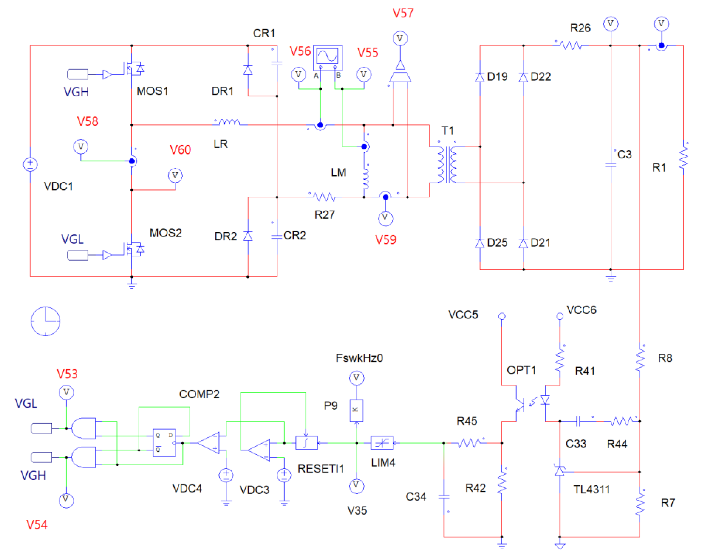
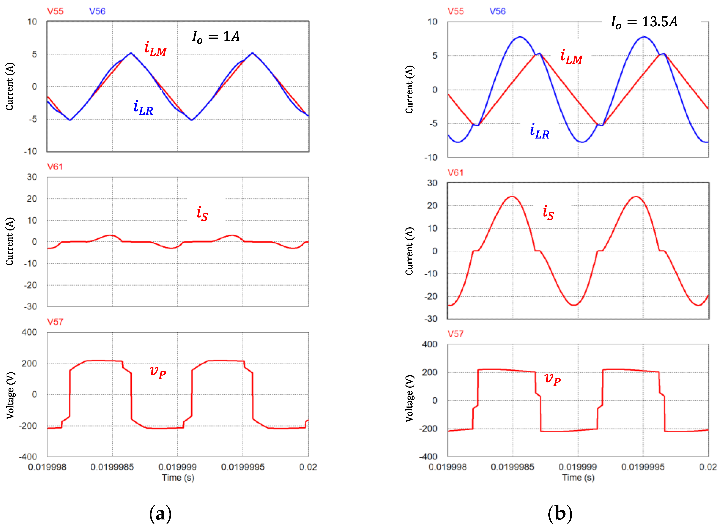
3.2. Circuit Simulation Results

In order to verify the LLC resonant converter designed in the previous section, a circuit simulation was performed. PSIM 11.0 was used for the simulation, and the designed circuit diagram is shown in Figure 10. In the figure, the abovementioned designed values were used for the main component values of the converter, and the main switches and rectifier diodes were modeled as ideal switches. To stabilize the output voltage, a voltage-controlled oscillator (VCO) circuit with a limited control frequency was applied. Figure 11 shows the resultant waveform of PSIM simulation when the converter operated in the steady-state. In Figure 11a, the load current is approximately 1 A, and in Figure 11b, the load current is approximately 13.5 A. These current values correspond to the approximate output power of 54 W and 730 W, respectively. In the figure, at the normal input voltage of 400 V, the switching frequency is close to the resonant frequency, and both the resonant inductor current, i L R , and the transformer secondary current, i S , show stable waveforms [33,34].

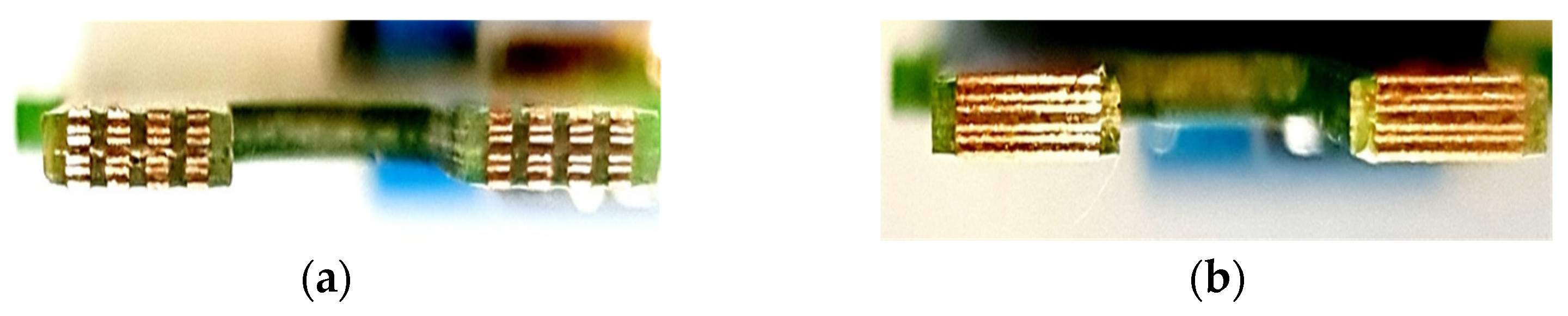
3.3. Wireless Power Transmission Transformer Design

Figure 12 shows the basic structure of the converter with the wireless power transmission transformer. In the figure, the LLC resonant converter is used as the basic circuit structure, and the air gap is formed using ceramic sheets for the transformer. To stabilize the output voltage, an IR photo tunnel was created in the ceramic insulating layers to transmit the error information regarding the output voltage and the reference voltage to the primary side. In order to miniaturize the wireless power transmission transformer proposed in this paper, a multilayered PCB winding, as shown in Figure 13, was applied. Figure 13a shows that there was a PCB winding composed of six layers between the magnetic core of the transformer and separated by ceramic insulating layers in the center. The winding of the multilayer structure was designed with a multilayer PCB pattern, the thickness of the copper foil for the PCB pattern was 4oz, and the winding resistance was reduced by applying the windings to each layer in parallel. Figure 13b shows how the primary and secondary magnetic flux inside the core of the wireless power transmission transformer were shared. Figure 14 shows the cross section of a multilayer PCB winding constructed with transformer windings. The total winding required on the primary side of the transformer was four turns, and each layer consisted of four turns. The PCB winding was a six-layer paralleled structure. The winding required on the secondary side was one turn, and as there was a relatively large current flow, it was designed in a parallel structure with a total of six layers [35,36,37].
Figure 15 shows the cross section of the converter to which the wireless power transmission transformer proposed in this paper was applied. The primary and secondary sides were separated around the ceramic insulating layers. To increase the mechanical strength, a thick ceramic layer was applied to the center, and a ceramic insulating layer was applied as the air gap of the transformer with a pre-designed thickness. Therefore, a total of two ceramic insulating layers, which were 0.38 mm and 1.0 mm in thickness, were used and overlapped with each other.
The converter in Figure 12 must deliver the error voltage information regarding the output voltage to the primary control element to stabilize the output voltage. As a photocoupler device for signal isolation generally used in a power supply has a horizontal structure, it is not suitable for use in a vertical structure of wireless power transmission. In this paper, we proposed the use of an IR photo tunnel structure, as shown in Figure 15, to solve this problem. First, a tunnel was created vertically on a ceramic insulating substrate, and the IR photo transmitter and receiver were designed facing each other through the ceramic tunnel so that the control signal could be transmitted [38]. The transmitting diode used in this experiment was a 940 nm class GaAlAs IR light-emitting diode. A light-blocking cap was added to block external light that have might interfered with the signal. Therefore, the DC–DC converter to which the wireless power transmission transformer was applied operated at a high switching frequency to reduce the size of the transformer, and had a structure that could diffuse the heat of the transformer to the ceramic insulating layer with high thermal conductivity. Figure 16 shows the internal structure and external appearance of the experimental converter constructed in this paper. Figure 16a shows the function and appearance of each layer separated vertically. From the top, the upper metal case, the primary-side PCB, the ceramic insulating layer as the air gap, the ceramic insulating layer for heat dissipation, the secondary-side PCB, and the bottom metal case are shown. The ferrite core of the transformer was directly attached to the ceramic insulating layer and the metal case. Therefore, the ceramic insulating layer and the metal case were thermally connected and served as a heat pipe, meaning internal heat could easily move to the case. Figure 16b shows the outline and size of the DC–DC converter to which the wireless power transmission transformer in the assembled state was applied [39]. The height of the power module was 10 mm, and terminals for input/output power and control signals were added. The power semiconductor switch was placed on a wide pattern of a multilayer PCB, heat-conductive tape was fixed inside the case to dissipate heat to the metal case, and the empty space inside the case was filled with a thermal-conductive epoxy encapsulating and potting compound [40,41].

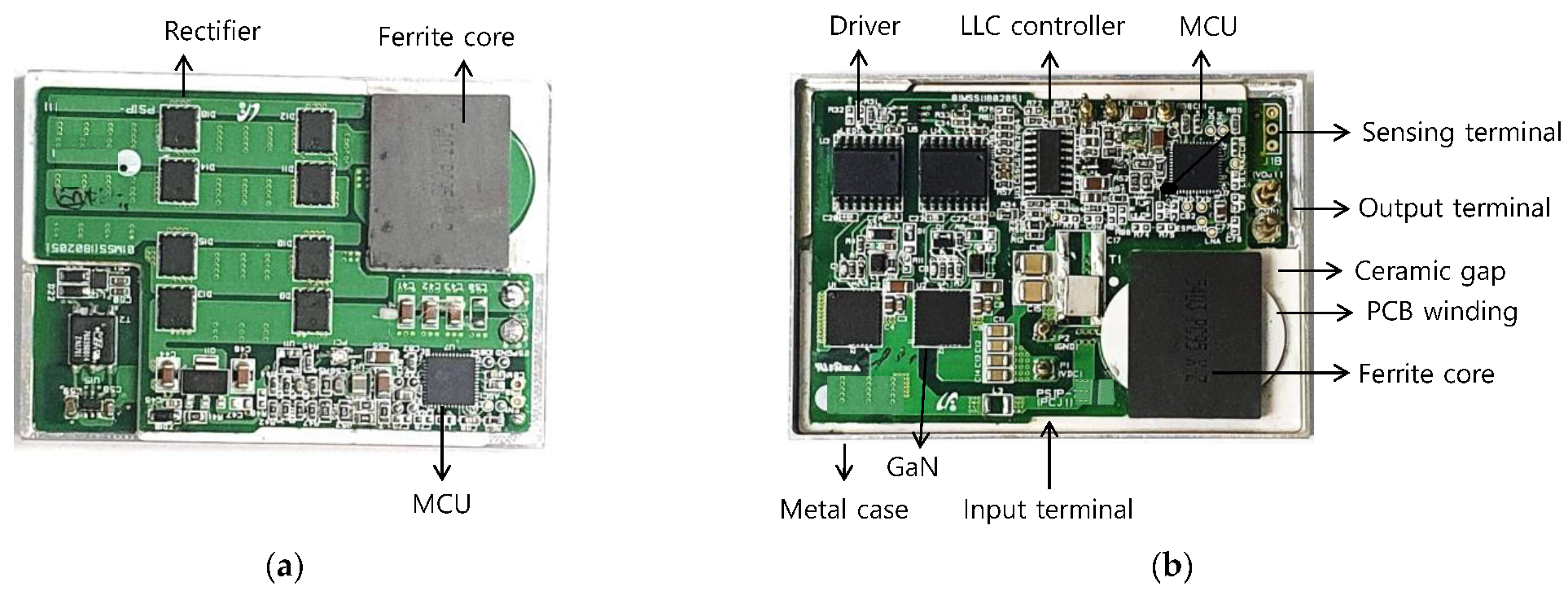
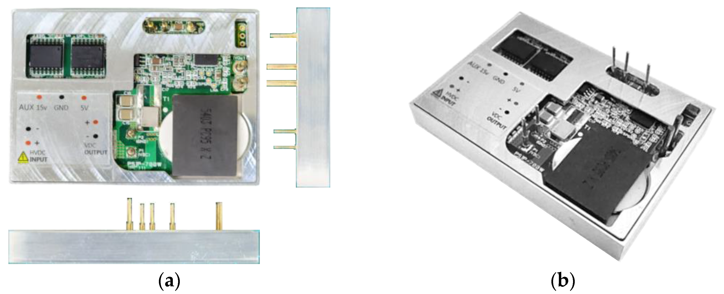
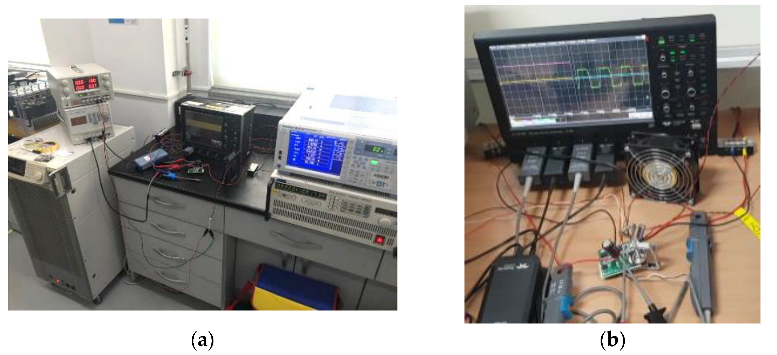
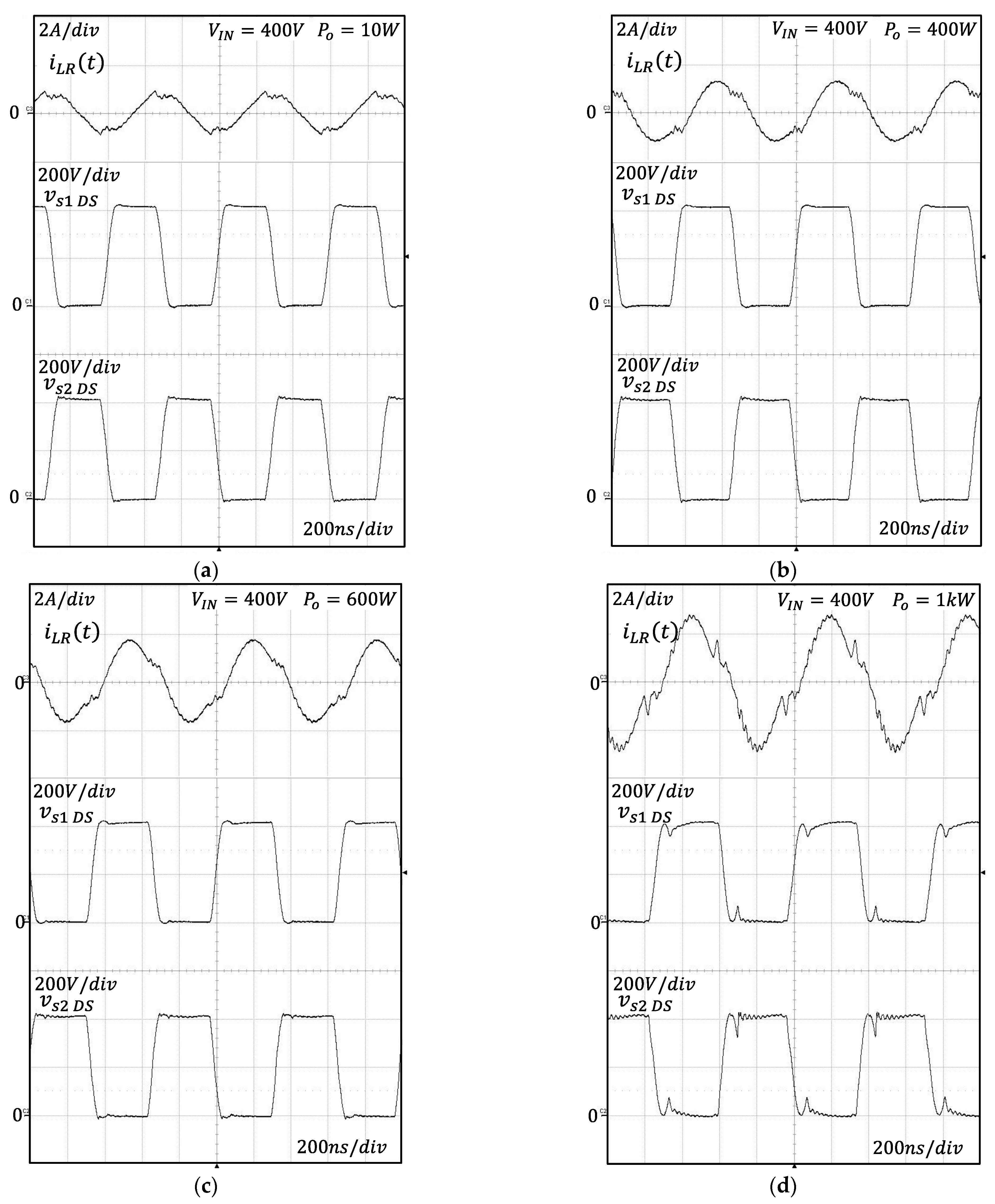
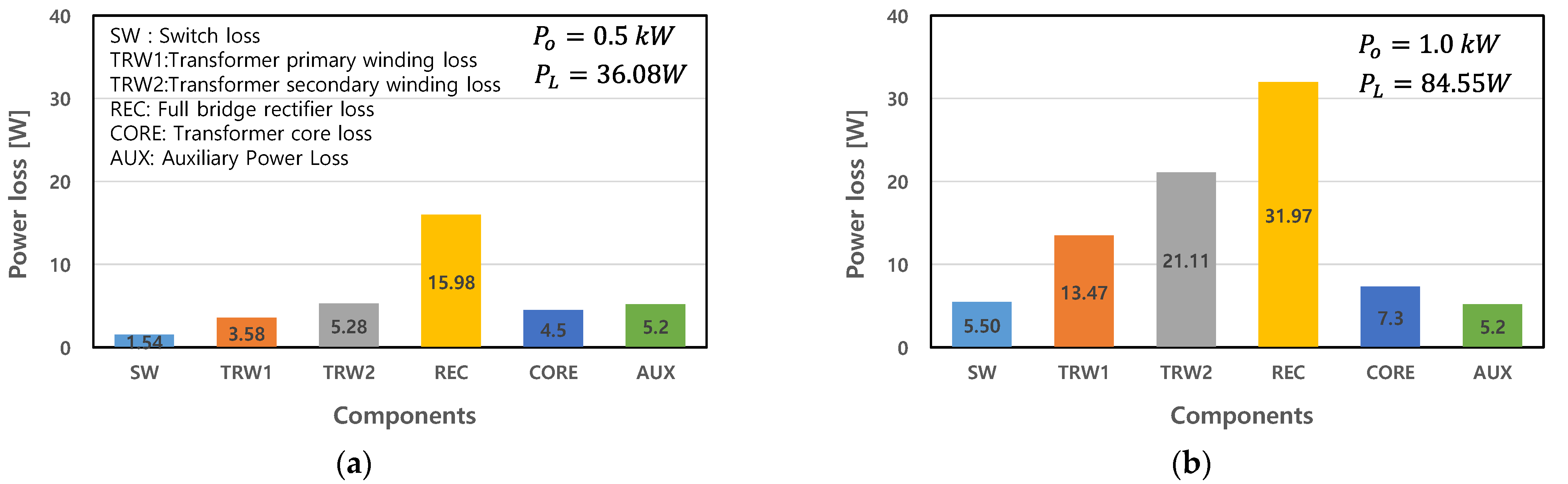
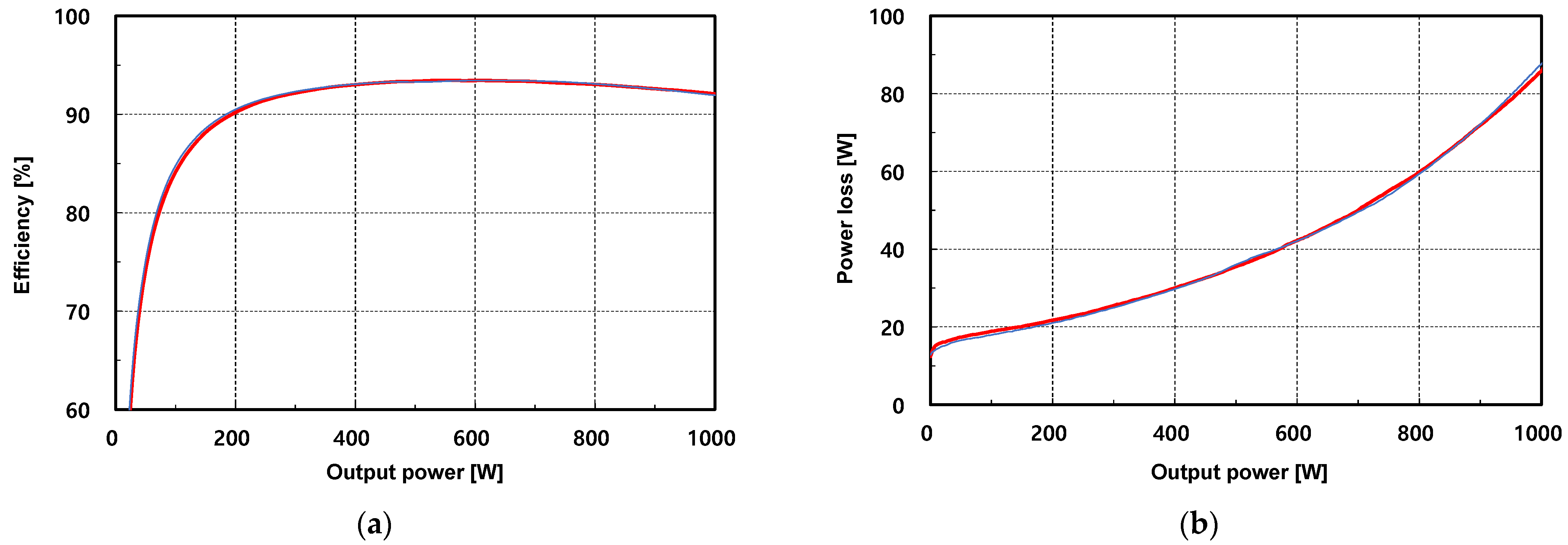
4. Experimental Results

An experimental circuit was made to verify the effectiveness of the wireless power transmission transformer structure and IR photo tunnel structure proposed in this paper. Table 2 shows the main components and electrical specifications used in the experimental circuit. As the experimental circuit operated at a switching frequency of 1 MHz or higher, a GaN FET suitable for high-frequency driving was applied as the main switch. The low-profile TDK ELT25 suitable for the PCB winding structure was used as the transformer ferrite core. To reduce the rectification loss of the secondary-side rectifier diode, two 170 V-class Schottky diodes were applied in parallel. The control IC of the converter used a 16-pin structure NCP1395 capable of achieving an operating frequency of 1 MHz or higher, and the IR photo transceiver was applied in a small package with a size of 2.3 mm in width and length.
Table 3 shows the power density of the experimental circuit. The maximum output of the DC–DC converter module to which the wireless power transmission transformer was applied was 1 kWm and the volume was 2.62 in 3 , meaning that the power density was approximately 382   W / in 3 . Figure 17 shows the internal structure of the primary-side PCB and secondary-side PCB of the experimental circuit. The transformer core with PCB windings was physically separated from the primary and secondary sides by the ceramic insulating layer, and a relatively wide PCB pattern was designed for the power semiconductor switches to facilitate thermal diffusion. Figure 18 is a photograph of the assembled experimental circuit. Inside the aluminum metal case, a 4oz, six-layer PCB winding wireless power transmission transformer and an IR photo tunnel structure power circuit were connected to each layer, and the empty space inside was filled with thermally conductive epoxy so that the internal heat could easily be diffused.
Figure 19 shows the test environment of the experimental circuit, and the test equipment used for the test were as follows: Oscilloscopes HDO6104 and 44MXs-B, input power PCR4000L and PCR4000LE, electronic loads PLZ1004WH and PLA5K-600-30, and input/output power meter WT1800 and WT1802E. Figure 20 shows the main waveforms of the experimental circuit operating in the steady-state. The waveforms are the resonant inductor current, i L R , and the voltages of the two main switches, v S 1 and v S 2 , from the top. At this time, the input voltage was 400 V, the output voltage was 54 V, and each waveform was observed by adjusting the output power. The output power was observed by dividing it into four sections from a minimum of 10 W to a maximum of 1 kW. The peak current of the resonant inductor was proportional to the output power and had a shape similar to a sine wave, and a relatively stable resonant current waveform was maintained over the entire load range.
Figure 21 shows the loss breakdown analysis of the experimental converter at 0.5 kW and 1 kW of output power. There were six major components involved in power loss in the converter: the main switches, transformer primary winding, transformer secondary winding, rectifier switches, transformer core and auxiliary power. Regardless of the output power, the rectifier switches on the secondary side caused the most power loss. At 0.5 kW of the load power, the total power loss of the major components was 36.08 W when the rectifier power loss was 15.98 W, which is approximately 44.3% of the total power loss. At 1 kW of the load power, the total power loss of the major components was 84.55 W when the rectifier power loss was 15.98 W, which is approximately 37.8% of the total power loss. Figure 22 shows the power conversion efficiency and loss of the experimental circuit in the steady-state. As can be seen from the graph of power conversion efficiency according to load power, when the output power was approximately 200 W or higher, the efficiency became more than 90%, and at the maximum load power, the efficiency was 91.9%. In the graph, the maximum power conversion efficiency was measured as approximately 93.4% at the output power of 600 W. The internal power dissipation ranged from a minimum of 13 W to a maximum of 86 W. Figure 23 shows a graph measuring the output voltage and switching frequency characteristics. The output voltage was measured as a maximum of 54.98 V and a minimum of 54.71 V over the full load range, resulting in an output voltage stability of less than approximately 0.49%. The switching frequency was inversely proportional to the load power, and in particular, the maximum switching frequency of 1.83 MHz at no load and 1.367 MHz at the maximum load was measured.
The experimental circuit for use in a communication device using the wireless power transmission transformer structure and IR photo tunnel structure proposed in this paper showed a high power density of over 380 W / in 3 and a high power conversion efficiency of up to 93.4%. From this result, it was considered to be practical as a basic structure of a modular power supply. In particular, as the primary side and the secondary side were physically separated by a ceramic insulating substrate, the manufacturing process could be simplified when a PCB winding was used. The two ceramic layers acted as heat pipes that transferred heat from the main components of the converter circuit to the aluminum metal case. As a result, most of the heat of the internal components could be easily balanced, which increased the reliability of the power supply.

5. Conclusions

In this study, we created a short-distance and fixed-type wireless power transmission transformer by modifying the transformer structure of a half-bridge LLC resonant converter. A ceramic insulating layer was used instead of an air gap, meaning the heat generated from the transformer core and the PCB winding was quickly transferred to the external metal case via the ceramic insulating layer, which acted as a heat pipe. In addition, in order to stabilize the output voltage, we proposed the use of the IR photo tunnel technology, and it was applied to two ceramic insulating layers so that the voltage error signal of the secondary output voltage could be transmitted as light to the primary side. As a result, it was possible to physically separate the primary and secondary side of the power circuit, centering on the ceramic insulating layer.
An experimental circuit was constructed to verify the effectiveness of the wireless power transmission transformer structure and IR photo tunnel structure proposed in this paper. The experimental circuit was applied to the power supply for communication devices that require high power density, and it was operated under the input voltage of 400 V, the output voltage of 54 V, the maximum output power of 1 kW, and the switching frequency of 1.3 MHz or higher. The optimal design was found using the steady-state characteristic equation with internal loss, and the optimal design process of the main components and the transformer was determined. In the experimental circuit, the power supply circuit including the transformer was put in a metal case, and the ceramic insulating layer was bonded inside the metal case for heat dissipation. As the primary and secondary sides of the power modules were physically separated by a ceramic insulating substrate, each could be produced separately, and the manufacturing process was simplified when PCB windings were used. In addition, the two ceramic layers acted as heat pipes which transferred heat from the main components of the converter circuit to the aluminum metal case. As a result, most of the heat in the internal components could easily be balanced, which increased the reliability of the power supply.
In the experimental circuit, the switching loss was reduced by applying GaN FETs, which has low loss characteristics in high switching frequency operation, for the two main switches. The control circuit was simplified by using the NCP1395 in the SO16 package which could operate over 1 MHz. The experiment showed stable operating waveforms with up to 1 kW output power in the steady-state. The maximum operating frequency was 1.83 MHz, and the output voltage stability to the load was 0.49% or less. The power density of the experimental circuit was 380 W / in 3 or higher, and the maximum power conversion efficiency was approximately 93% or higher. From these results, we consider the wireless power transmission transformer, IR photo tunnel, and ceramic heat pipe technology proposed in this paper to have practical value in designing high-power density modular power supplies.

Author Contributions

Conceptualization, T.-Y.A.; Methodology, J.-S.Y., Y.-M.G. and T.-Y.A.; Validation, J.-S.Y., Y.-M.G. and T.-Y.A.; Formal analysis, T.-Y.A.; Investigation, J.-S.Y. and Y.-M.G.; Resources, T.-Y.A.; Data curation, Y.-M.G. and T.-Y.A.; Writing—original draft preparation, J.-S.Y., Y.-M.G. and T.-Y.A.; Writing—review and editing, J.-S.Y., Y.-M.G. and T.-Y.A.; Visualization, J.-S.Y. and T.-Y.A.; Supervision, Y.-M.G. and T.-Y.A.; Project administration, Y.-M.G. and T.-Y.A.; Funding acquisition, T.-Y.A. All authors have read and agreed to the published version of the manuscript.

Funding

This work was supported by the Industrial Strategic Technology Development Program- Automobile Industry Technology Development (1415180408, Development of common component technology for power steering and braking systems for hydrogen electric commercial vehicles) funded by the Ministry of Trade, Industry & Energy (MOTIE, Korea).

Data Availability Statement

Not applicable.

Conflicts of Interest

The authors declare no conflict of interest.

References

  1. Leandro, G.M.; Barbi, I.; Akhbari, M. Switched-Capacitor LLC Resonant DC-DC Converter with Switch Peak Voltage of Vin/2. IEEE Access 2020, 8, 111504–111513. [Google Scholar] [CrossRef]
  2. Lee, I.O.; Moon, G.W. The k-Q Analysis for an LLC Series Resonant Converter. IEEE Trans. Power Electron. 2013, 29, 13–16. [Google Scholar] [CrossRef]
  3. Beiranvand, R.; Rashidian, B.; Zolghadri, M.R.; Hossein Alavi, S.M. A Design Procedure for Optimizing the LLC Resonant Converter as a Wide Output Range Voltage Source. IEEE Trans. Power Electron. 2012, 27, 3749–3763. [Google Scholar] [CrossRef]
  4. Hu, Z.; Wang, L.; Wang, H.; Liu, Y.F.; Sen, P.C. An Accurate Design Algorithm for LLC Resonant Converters—Part I. IEEE Trans. Power Electron. 2016, 31, 5435–5447. [Google Scholar] [CrossRef]
  5. Fei, C.; Lee, F.C.; Li, Q. High-Efficiency High-Power-Density LLC Converter with an Integrated Planar Matrix Transformer for High-Output Current Applications. IEEE Trans. Ind. Electron. 2017, 64, 9072–9082. [Google Scholar] [CrossRef]
  6. Zheng, R.; Liu, B.; Duan, S. Planar Transformers in LLC Resonant Converters: High-Frequency Fringing Losses Modeling. IEEE Trans. Power Electron. 2015, 30, 7113–7122. [Google Scholar] [CrossRef]
  7. Shafaei, R.; Perez, M.C.G.; Ordonez, M. Equivalence Relations of Resonant Tanks: A New Perspective for Selection and Design of Resonant Converters. IEEE Trans. Power Electron. 2020, 35, 9632–9649. [Google Scholar] [CrossRef]
  8. Fang, X.; Hu, H.; Chen, F.; Somani, U.; Auadisian, E.; Shen, J.; Batarseh, I. Efficiency-Oriented Optimal Design of the LLC Resonant Converter Based on Peak Gain Placement. IEEE Trans. Power Electron. 2013, 28, 2285–2296. [Google Scholar] [CrossRef]
  9. Kim, B.-C.; Park, K.-B.; Kim, C.-E.; Lee, B.-H.; Moon, G.-W. LLC Resonant Converter with Adaptive Link-Voltage Variation for a High-Power-Density Adapter. IEEE Trans. Power Electron. 2010, 25, 2248–2252. [Google Scholar] [CrossRef]
  10. Ji, S.; Reusch, D.; Lee, F.C. High-frequency high power density 3-d integrated gallium-nitride-based point of load module design. IEEE Trans. Power Electron. 2013, 28, 4216–4226. [Google Scholar] [CrossRef]
  11. Mou, X.; Gladwin, D.T.; Zhao, R.; Sun, H. A Survey on Magnetic Resonant Coupling Wireless Power Transfer Technology for Electric Vehicle Charging. IET Power Electron. 2019, 12, 3005–3020. [Google Scholar] [CrossRef] [Green Version]
  12. Li, G.; Xia, J.; Wang, K.; Deng, Y.; He, X.; Wang, Y. Hybrid Modulating of Parallel-Series LLC Resonant Converter and Phase Shift Full-Bridege Converter for a Dual-Output DC-DC Converter. IEEE Trans. Power Electron. 2019, 7, 833–842. [Google Scholar] [CrossRef]
  13. Qian, T.; Qian, C. An Adaptive Frequency Optimization Scheme for LLC Converter with Adjustable Energy Transferring Time. IEEE Trans. Power Electron. 2019, 34, 2018–2024. [Google Scholar] [CrossRef]
  14. Da Silva, R.L.; Borges, V.L.F.; Possamai, C.E.; Barbi, I. Solid-State Transformer for Power Distribution Grid Based on a Hybrid Switched-Capacitor LLC-SRC Converter: Analysis, Design, and Experimentation. IEEE Access. 2020, 8, 141182–141207. [Google Scholar] [CrossRef]
  15. Li, X.; Tsui, C.-Y.; Ki, W.-H. A 13.56 MHz Wireless Power Transfer System with Reconfigurable Resonant Regulating Rectifier and Wireless Power Control for Implantable Medical Devices. IEEE J. Solid-State Circuits 2015, 50, 978–989. [Google Scholar] [CrossRef]
  16. Guo, J.; Tan, L.; Liu, H.; Wang, W.; Huang, X. Stabilization Control of Output Power in Double-Source Wireless Power Transfer Systems without Direct Output Feedback. IEEE Microw. Wirel. Compon. Lett. 2016, 26, 960–962. [Google Scholar] [CrossRef]
  17. Glitz, E.S.; Ordonez, M. MOSFET Power Loss Estimation in LLC Resonant Converters: Time Interval Analysis. IEEE Trans. Power Electron. 2019, 34, 11964–11980. [Google Scholar] [CrossRef]
  18. Duan, J.; Zhang, D.; Gu, R. Partial-Power Post-Regulated LLC Resonant DC Transformer. IEEE Trans. Ind. Electron. 2022, 69, 7909–7919. [Google Scholar] [CrossRef]
  19. Sample, A.P.; Meyer, D.T.; Smith, J.R. Analysis, experimental results, and range adaptation of magnetically coupled resonators for wireless power transfer. IEEE Trans. Ind. Electron. 2011, 58, 544–554. [Google Scholar] [CrossRef]
  20. Kim, D.K.; Moon, S.; Yeon, C.O.; Moon, G.W. High-Efficiency LLC Resonant Converter with High Voltage Gain Using an Auxiliary LC Resonant Circuit. IEEE Trans. Power Electron. 2016, 31, 6901–6909. [Google Scholar] [CrossRef]
  21. Xu, H.; Yin, Z.; Zhao, Y.; Huang, Y. Accurate Design of High-Efficiency LLC Resonant Converter with Wide Output Voltage. IEEE Access 2017, 5, 26653–26665. [Google Scholar] [CrossRef]
  22. Liu, J.; Zhang, J.; Zheng, T.Q.; Yang, J. A Modified Gain Model and the Corresponding Design Method for an LLC Resonant Converter. IEEE Trans. Power Electron. 2017, 32, 6716–6727. [Google Scholar] [CrossRef]
  23. Chen, S.Y.; Li, Z.R.; Chen, C.L. Analysis and Design of Single-Stage AC/DC LLC Resonant Converter. IEEE Trans. Ind. Electron. 2012, 59, 1538–1544. [Google Scholar] [CrossRef]
  24. Fang, X.; Hu, H.; Shen, Z.J.; Batarseh, I. Operation Mode Analysis and Peak Gain Approximation of the LLC Resonant Converter. IEEE Trans. Power Electron. 2012, 27, 1985–1995. [Google Scholar] [CrossRef]
  25. Yoo, J.-S.; Gil, Y.-M.; Ahn, T.-Y. Steady-State Analysis and Optimal Design of an LLC Resonant Converter Considering Internal Loss Resistance. Energies 2022, 15, 8144. [Google Scholar] [CrossRef]
  26. Mayordomo, I.; Dräger, T.; Spies, P.; Bernhard, J.; Pflaum, A. An Overview of Technical Challenges and Advances of Inductive Wireless Power Transmission. Proc. IEEE 2013, 101, 1302–1311. [Google Scholar] [CrossRef]
  27. Jung, J.H.; Kim, H.S.; Ryu, M.H.; Baek, J.W. Design Methodology of Bidirectional CLLC Resonant Converter for High-Frequency Isolation of DC Distribution Systems. IEEE Trans. Power Electron. 2013, 28, 1741–1755. [Google Scholar] [CrossRef]
  28. Duan, F.; Xu, M.; Yang, X.; Yao, Y. Canonical Model and Design Methodology for LLC DC/DC Converter with Constant Current Operation Capability under Shorted Load. IEEE Trans. Power Electron. 2016, 31, 6870–6883. [Google Scholar] [CrossRef]
  29. Yang, C.H.; Liang, T.J.; Chen, K.H.; Li, J.S.; Lee, J.S. Loss analysis of half-bridge LLC resonant converter. In Proceedings of the 2013 1st International Future Energy Electronics Conference (IFEEC), Tainan, Taiwan, 3–6 November 2013; pp. 155–160. [Google Scholar] [CrossRef]
  30. Hu, S.; Deng, J.; Mi, C.; Zhang, M. Optimal design of line level control resonant converters in plug-in hybrid electric vehicle battery chargers. IET Electr. Syst. Transp. 2014, 4, 21–28. [Google Scholar] [CrossRef]
  31. Yang, Y.; Zhang, L.; Ma, T. Conduction Loss Analysis and Optimization Design of Full Bridge LLC Resonant Converter. In Proceedings of the 2018 International Power Electronics Conference (IPEC-Niigata 2018 -ECCE Asia), Niigata, Japan, 20–24 May 2018; pp. 2703–2707. [Google Scholar] [CrossRef]
  32. Kim, J.; Moon, G. A new LLC natural resonant converter with narrow switching frequency variation and reduced conduction losses. IEEE Trans. Power Electron. 2014, 29, 4278–4287. [Google Scholar] [CrossRef]
  33. Beiranvand, R.; Rashidian, B.; Zolghadri, M.; Alavi, S.M. Using LLC resonant converter for designing wide-range voltage source. IEEE Trans. Ind. Electron. 2011, 58, 1746–1756. [Google Scholar] [CrossRef]
  34. Zhao, C.; Wu, X.; Meng, P.; Qian, Z. Optimum design consideration and implementation of a novel synchronous rectified soft-switched phase-shift full-bridge converter for low-output-voltage high-output-current applications. IEEE Trans. Power Electron. 2009, 24, 388–397. [Google Scholar] [CrossRef]
  35. Chen, W.; Xu, M.; Ge, Y.; Guo, Q.; Jiang, T.; Che, X. Parameter Design of High Power LLC Resonant Converter. In Proceedings of the 2022 IEEE 5th International Conference on Electronics Technology (ICET), Chengdu, China, 13–16 May 2022; pp. 421–425. [Google Scholar] [CrossRef]
  36. Jami, M.; Beiranvand, R.; Mohamadian, M.; Ghasemi, M. Optimization the LLC resonant converter for achieving maximum efficiency at a predetermined load value. In Proceedings of the 6th Power Electronics, Drive Systems & Technologies Conference (PEDSTC2015), Tehran, Iran, 3–4 February 2015; pp. 149–155. [Google Scholar] [CrossRef]
  37. Katayama, Y.; Sugahara, S.; Nakazawa, H.; Edo, M. High-power-density MHz-switching monolithic DC-DC converter with thin-film inductor. In Proceedings of the IEEE 31st Annual Power Electronics Specialists Conference. Conference Proceedings, Galway, Ireland, 23–23 June 2000; Volume 3, pp. 1485–1490. [Google Scholar] [CrossRef]
  38. Ahn, T.Y. A Study on Steady State Characteristics of LLC Resonant Half Bridge Converter Considering Internal Losses. IKEEE 2018, 22, 985–991. [Google Scholar] [CrossRef]
  39. Yoon, K.H.; Noh, Y.J.; Phum, S.; Meas, S.; Jang, S.H.; Kim, E.S. LLC resonant converter with wide input voltage and load range at fixed switching frequency. In Proceedings of the 2012 Twenty-Seventh Annual IEEE Applied Power Electronics Conference and Exposition (APEC), Orlando, FL, USA, 5–9 February 2012; pp. 1338–1342. [Google Scholar] [CrossRef]
  40. Yang, B.; Lee, F.C.; Zhang, A.J.; Huang, G. LLC resonant converter for front end DC/DC conversion. In Proceedings of the APEC. Seventeenth Annual IEEE Applied Power Electronics Conference and Exposition (Cat. No.02CH37335), Dallas, TX, USA, 10–14 March 2002; Volume 2, pp. 1108–1112. [Google Scholar] [CrossRef]
  41. Ivensky, G.; Bronshtein, S.; Abramovitz, A. Approximate Analysis of Resonant LLC DC-DC Converter. IEEE Trans. Power Electron. 2011, 26, 3274–3284. [Google Scholar] [CrossRef]
Figure 1. A basic circuit structure of an LLC resonant converter.
Energies 15 09006 g001
Figure 2. The steady-state operating waveform of an LLC resonant converter (a) when the switching frequency and the resonant frequency are similar and (b) when the switching frequency and resonant frequency are large.
Energies 15 09006 g002
Figure 3. LLC resonant converter with wireless power transmission transformer.
Energies 15 09006 g003
Figure 4. Wireless power transmission transformer, (a) structure of wireless power transmission transformer, (b) equivalent circuit of the wireless power transmission transformer.
Energies 15 09006 g004
Figure 5. Wireless power transmission converter including parasitic elements of the wireless power transmission transformer.
Energies 15 09006 g005
Figure 6. Thermal diffusion structure using a wireless power transmission transformer and a ceramic insulating plate.
Energies 15 09006 g006
Figure 7. Operating area of the LLC converter.
Energies 15 09006 g007
Figure 8. Frequency characteristics of the DC voltage gain, M. (a) DC voltage gain over load range, Q, and (b) DC voltage gain, M, in accordance with inductance ratio, K L .
Energies 15 09006 g008
Figure 9. Switching frequency characteristics for load range, Q. (a) Switching frequency characteristics for input voltage and (b) normalized frequency characteristics for voltage gain.
Energies 15 09006 g009
Figure 10. PSIM simulation schematic of the wireless power transmission converter.
Energies 15 09006 g010
Figure 11. Steady-state waveform result of the wireless power transmission converter with PSIM simulation (a) at low load power and (b) at large load power.
Energies 15 09006 g011
Figure 12. Basic structure of a high-power-density converter using a wireless power transmission transformer.
Energies 15 09006 g012
Figure 13. The structure of a wireless power transmission transformer using a ceramic insulating layer. (a) Transformer structure using laminated PCB winding and (b) structure and magnetic flux of a wireless power transmission transformer.
Energies 15 09006 g013
Figure 14. Laminated PCB winding structure. (a) Primary-side laminated PCB winding structure of the transformer and (b) secondary-side laminated PCB winding structure of the transformer.
Energies 15 09006 g014
Figure 15. Insulated signal transmission method using an IR photodiode.
Energies 15 09006 g015
Figure 16. High-power-density converter with a ceramic insulation substrate and wireless power transmission transformer. (a) Basic structure of the converter separated by a ceramic insulation layer and (b) high-power-density converter in a heat dissipation metal case.
Energies 15 09006 g016
Figure 17. Internal structure of the experimental module. (a) Internal structure of secondary side of experimental module and (b) internal structure of the primary side of the experimental module.
Energies 15 09006 g017
Figure 18. External appearance of the high-power density module for the experiment. (a) Side views of the experimental module and (b) experimental module in a metal case with external terminals.
Energies 15 09006 g018
Figure 19. Experimental circuit and experiment configuration photograph. (a) Load testing of converters and (b) steady-state test of the converter.
Energies 15 09006 g019
Figure 20. Experimental closed-loop waveform in steady-state. (a) Output power of 10 W, (b) output power of 400 W, (c) output power of 600 W, (d) output power of 1 kW.
Energies 15 09006 g020
Figure 21. Loss breakdown analysis of an experimental converter. (a) Output power of 0.5 kW, (b) output power of 1 kW.
Energies 15 09006 g021
Figure 22. Efficiency and loss characteristics of an experimental converter. (a) Power conversion efficiency characteristics of the experimental converter and (b) internal power dissipation characteristics of the experimental converter.
Energies 15 09006 g022
Figure 23. Load characteristics and switching frequency of the experimental converter. (a) Load characteristics of the experimental converter and (b) switching frequency characteristics of an experimental converter.
Energies 15 09006 g023
Table 1. Design conditions for LLC resonant converters.
ParameterVariableValueUnit
Input voltage range V I N 360–400V
Nominal input voltage V I N   ( n o m ) 390V
Output voltage V o 54V
Maximum output power P o   m a x 1.0kW
Maximum output current I o   m a x 18.5A
Resonant frequency f o 1.1MHz
Inductance ratio K L 3-
Table 2. Electrical ratings of the main components used in the experimental circuit.
ParameterVariableValueSpecifications
Main switch model S 1 , 2 LMG3410GaN 600 V, 12 A, 70 mΩ
Resonant capacitor C R 6     nF 2   nF × 3
Resonant inductor L R 3.5     μ H TDK ELT25 X 8.6
Magnetizing inductor L M 9.5   μ H TDK ELT25 X 8.6
Transformer turns ratio N 8:2TDK ELT25 X 8.6
Rectifier switch model D 1 , 2 , 3 , 4 STPS30170DJF170 V, 30 A
PFM controllerICNCP13951.0 MHz, 20 V
IR couplerICVEMT2003X20 V, 50 mA
Output capacitance C o 8.8 μF2.2 μF × 4
Table 3. External size and power density of the experimental module.
ParameterVariableValue (cm)Value (in)
Maximum power P o   m a x 1 kW1 kW
Width l W 5.5 cm 2.17   in
Length l L 7.8 cm 3.07   in
Height l H 1.0 cm 0.39   in
Volume V 42.9   cm 3 2.62   in 3
Power densityPD 23   W / cm 3 382   W / in 3
Publisher’s Note: MDPI stays neutral with regard to jurisdictional claims in published maps and institutional affiliations.

