2. Regulator Model
Most integrated switching voltage regulators currently available on the market have the following main features and parameters:
An input supply voltage terminal Vin, which is usually in a range of up to 40 V, and for higher voltage regulators, the input voltage can be up to 60 V;
A GND terminal as a negative power supply voltage terminal;
An ON/OFF terminal, which is a control terminal that can activate or deactivate the operation of the regulator;
An FB (feedback) terminal to compare output voltage with a fixed built-in reference voltage Vref, which helps to regulate the desired output voltage level;
An OUT terminal to connect other external components, such as a diode D, an inductor L, a capacitor C, a resistance R etc.;
Fixed switching frequency f;
Built-in current protection for the internal power switch of the regulator with the value Imax;
The specified amount of current IQ, which is taken by the regulator chip itself from the power supply;
Specified amount of voltage drop Vsat on the regulator, at maximum current and switch S closed;
Entered maximum duty factor Dmax;
Specified range of resistance values of resistor R1 (according to
Figure 1).
For the designed model of the controller to be universal, it must be able to reflect all the above-mentioned properties and parameters. Based on that, it is possible to draw its block diagram shown in
Figure 2.
The operation of the proposed controller is as follows. The basis is a frequency generator (clock freq.). It generates a rectangular signal with the required switching frequency of the controller and a duty factor equal to
Dmax. The amplitude of the output signal is 5 V due to its further processing using TTL circuits. At the rising edge of its output signal, the monostable flip-flop circuit 1 generates, at its output
, a short pulse with a logic level of
L, and the pulse feeds the input S of the R-S flip-flop circuit. This sets its output to a logic H value. If a logic
L is present at the ON/OFF input, the logic H is transmitted via the AND gate to the voltage-controlled switch S, which turns on. The closed-state resistance of the switch must be set according to the following relation:
In a similar way, the off-state switch resistant
is given by:
where
Vin is the value of the supply voltage, and
IL is the value of the output leakage current of the regulator in the off state. A monostable flip-flop 2 is connected to the falling edge of the signal from the frequency generator. It generates a short pulse at its output Q. This pulse is transmitted through the gate NOR2 to the R input of the R-S flip-flop circuit. This flips the R-S circuit to logic
L. It also causes the voltage-controlled switch S of the controller to switch off via the AND gate. There are two ways to shorten the maximum pulse duration, either by exceeding the maximum permissible current
Imax of the regulator or by exceeding the required output voltage. The first case is treated by sensing the current of the switch with ammeter A. If its value exceeds the value
Imax, the current control switch is switched on. The logic
H is applied to the second of the NOR2 inputs. This ensures premature switching of the output of the R-S flip-flop circuit to the logic
L before reaching
Dmax and, thus, the duration of the switching pulse shortening. The second case is treated with voltage-controlled switch 2, which is switched when the value of the voltage at the input FB (feedback) exceeds the value of the internal reference voltage
Vref of the controller. In this case, the logic
H is again applied to the third of the NOR2 inputs and shortens the duration of the switching pulse of the regulator below the value
Dmax. The ensuring of the logic
L values at the inputs two and three of NOR2 is realized by a pair of resistors
R. Blocking of the controller operation is ensured by a signal fed to the ON/OFF input of the regulator, which is further inverted by member NOR1, whose output is the second input of the
AND gate. If the value of logic
H at the ON/OFF input is exceeded, it is inverted to the level of logic
L via
NOR1. The transmission of control signals for the voltage-controlled switch S through the AND gate is blocked. The simulation of the internal current consumption
IQ of the regulator is realized by means of the resistor R
int, the value of which is given by the ratio:
where
Vin is the supply voltage and
IQ is the supply current of the controller. Exceeding the supply voltage
Vin leads to a break in the switch on the real component and usually disconnects the circuit. The task of this fact is to simulate voltage-controlled switch 1. It is opened by exceeding the value
Vin sensed by the voltmeter V above the value
Vmax.
In order to implement the proposed model of a universal voltage regulator, it is advantageous to use the widely used PSpice program [
19] or one of its equivalents. In our case, this is a TINA program [
20] (Toolkit for interactive network analysis). The program library can be supplemented in the form of a subcircuit based on the PSpice program rules [
21,
22,
23].
PSpice software is a widely used and accepted standard for many electrical circuit simulation software [
24,
25]. Many producers offer a spice model for their products. In order to make the sub-circuit more user-friendly, it is possible to covert text notation in the graphic form using regulator graphics symbols. Only variable parameters would be editable by the user. In our case, this was the following parameters:
f,
Vref,
Imax,
Rsw,
Dmax,
Vmax, and
Rint. Since each real regulator is individual, the triggering of their oscillators is random. Therefore, we added the Delay parameter to the model. The user can set individual modes of the regulator’s time operation even in the case of multiple uses in one connection. The text notation of the universal model is presented in
Appendix A.
The integrated switching voltage regulator LM2576 serves to show a graphical presentation of the model. An interactive dialog box allowing the main parameters of the model to be changed in the graphical presentation of the model is shown in
Figure 3.
The LM2576 controller using the catalog parameters was chosen for the first proof of the correct operation of the proposed simulation model. The output voltage of the converter with the given regulator can be calculated from the relation [
14]:
where
Vref has a value of 1.23 V. The circuit was supplemented by external components with the values recommended by the manufacturer:
L = 100 μH,
R5 = 460 mΩ,
Vin = 40 V,
R1 = 2 kΩ,
R2 = 22.39 kΩ,
C1 = 100 μF,
C2 = 1 mF, and
Rc = 181 mΩ. The SD1 diode was selected as MBR360. The load resistor has a value of
RL = 5 Ω. The overall connection of the inverter with the controller model and external components is shown in
Figure 4. The resulting waveforms obtained by the simulation are shown in
Figure 5.
Validation of the correct operation of the converter can be performed by comparing the results obtained by the simulation with the results obtained by the measurement showed in
Figure 6, which is stated by the manufacturer in the datasheet for the component [
14].
In addition to the static activity verification, it is also necessary to verify the reliability and fidelity of the model during the dynamic operation. This can be performed by comparing the waveforms obtained by the simulation and the waveforms measured by the manufacturer [
14]. The analyzed circuit is shown in
Figure 7. The values of the circuit elements are the same as the circuit in
Figure 4. Only the load resistance RL2 with a value of 32.5 Ω was added. The results obtained by the simulation are shown in
Figure 8, and the catalog curves are shown in
Figure 9.
The model sufficiently corresponds to the real component in a static state (
Figure 5 vs.
Figure 6) and a dynamic state (
Figure 8 vs.
Figure 9) when comparing model results and data given by the manufacturer. Based on this, the model can be further used to investigate the behavior of a newly designed circuit.
3. Universal Model Comparing with Existing LM 2576HV PSpice Models and a Real 2576HV
There is no other universal buck DC–DC converter model found on the Internet. There are, of course, general buck DC–DC converter schematics, but none of them has an implementation of the variable properties such as switching frequency, current and voltage limitations, feedback voltage, etc. In order to determine universal model accuracy, it was compared with official PSpice models and with the real item. A standard LM2576 converter was out of stock in all the relevant shops—possibly due to the semiconductor component crisis—so the closest alternative, an LM2576HV from Texas Instruments, was chosen. Texas Instruments (TI) offers official PSpice models for many of their products, including the LM2576HV; therefore, the universal model could be compared with the model officially provided by the manufacturer. The real DC–DC converter based on the TI LM2576HV is shown in
Figure 10.
The two wire loops that can be seen on the bottom of the PCB are used for current measurement, where current from the switch (
Isw) and current through the coil (
IL) (according to
Figure 5) are measured. Moreover, other circuits component values from the
Figure 4 circuit were updated according to the real component as follows:
L = 108 μH, R5 = 103 mΩ,
Vin = 45 V,
R1 = 3.1 kΩ,
R2 = 9.5 kΩ,
C1 = 100 μF,
C2 = 883 μF, and
Rc = 61 mΩ. The SD1 diode was implemented by an MBR1645. The real component’s value was measured on a HAMEG HM8118 LCR bridge. The load resistance, including parasite resistance, was calculated from the load voltage and load current measured using an oscilloscope and the resulting resistance value was
RL = 1.79 Ω.
Official PSpice models, including datasheet, were taken from the official product web [
11]. Texas instruments offer many products PSpice models. The offered PSpice models can be in the form of an encrypted full PSpice component or an unencrypted PSpice script. Encrypted models can be used in the PSpice application only, whereas unencrypted PSpice script models can also be used in other simulation software supporting the PSpice script, including TINA. Both types of PSpice models are available for the LM2576HV. This allows three models (universal, encrypted, and unencrypted) to be compared with the real LM2576HV converter. The simulation based on the encrypted PSpice model was performed on PSpice-TI [
19] software, and simulations based on universal and unencrypted models were performed on TINA-TI software [
20]. The circuit components and their values were identical except for the switching regulator model itself. The universal model parameters were updated from the original LM2576 parameter values (
Figure 3) to LM2576HV according to the datasheet [
26], where new setting values are shown in the Parameter Editor Windows in
Figure 11.
The real measurement was performed with a Tektronix DPO7354 oscilloscope, and the currents were measured using Tektronix TCP0030 current probes. The measuring laboratory [
27] is shown in
Figure 12.
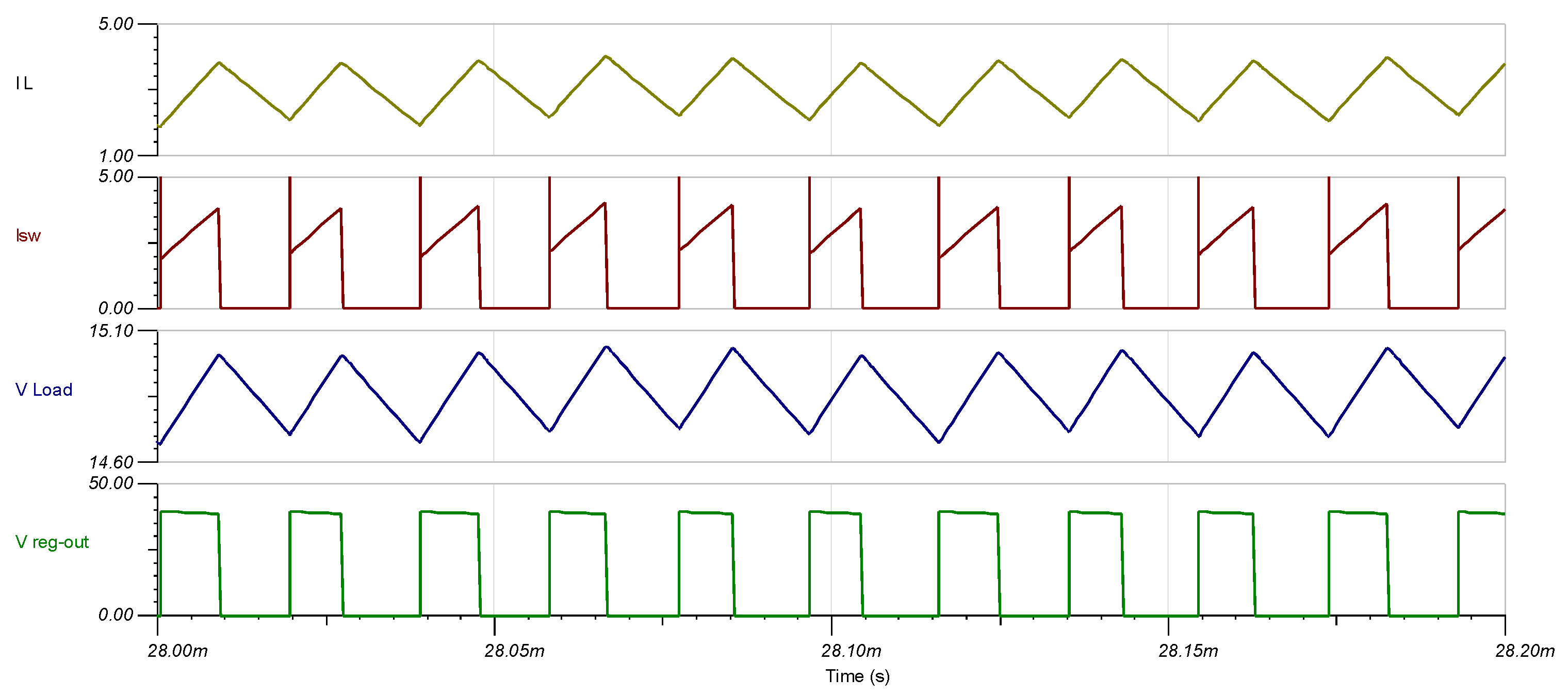
First, the steady-state circuit parameters were compared. The parameters mentioned in
Figure 5 and
Figure 6 were measured and compared with the simulations. An example of a steady-state measurement is shown in
Figure 13.
For a better comparison, the measured and simulated values were exported and put together into one graph via MS Excel. This showed that the graph curves are very similar; therefore, the different details are also shown in the graphs below. A real measurement cannot be performed in a specific time, but in the steady-state repeating graph curves, the specific time is not as important. The time of the first positive edge of the measured Vreg-out signal was synchronized with the first positive edge of the Vreg-out signal of the universal model. In order to make the simulations more effective, parameters (Isw, Vreg-out, IL, VLoad from the beginning time (t = 0) were observed. The simulations showed that the transient response on start takes approximately 1.6 ms, and after that, the regulator works on its work point. The curves after 2nd ms were investigated.
First, the voltage from the regulator (
Vreg-out) comparison is shown in
Figure 14, and differences in the details are shown in
Figure 15.
Figure 14 shows that all the time graph curves are similar. More significant differences can be seen from an unencrypted model where a certain level of instability can be observed. Generally, the signal from the universal model and encrypted model are very close in shape, amplitude, and frequency to each other and to the measured signal. A more detailed look at the amplitude differences is shown in
Figure 15.
The current time course comparison from the regulator (
Isw) is shown in
Figure 16.
As can be seen in
Figure 16, the impulses are similar to each other. A more detailed illustration is shown in
Figure 17. Moreover, the unencrypted model seems to be more unstable compared to the universal and encrypted models.
The current peaks are not in all pulses in curves calculated by TINA software. The current peaks caused by the Schottky diode capacity are very short (approximately 100 ps). The simulation results were calculated in specific discrete time steps. The reason for missing current peaks in some signal curves is that the TINA software time steps skipped the occurrence of the current peaks. A TINA simulation with a maximum time step of 10 ps would create 10 million values for a 100 µs time simulation.
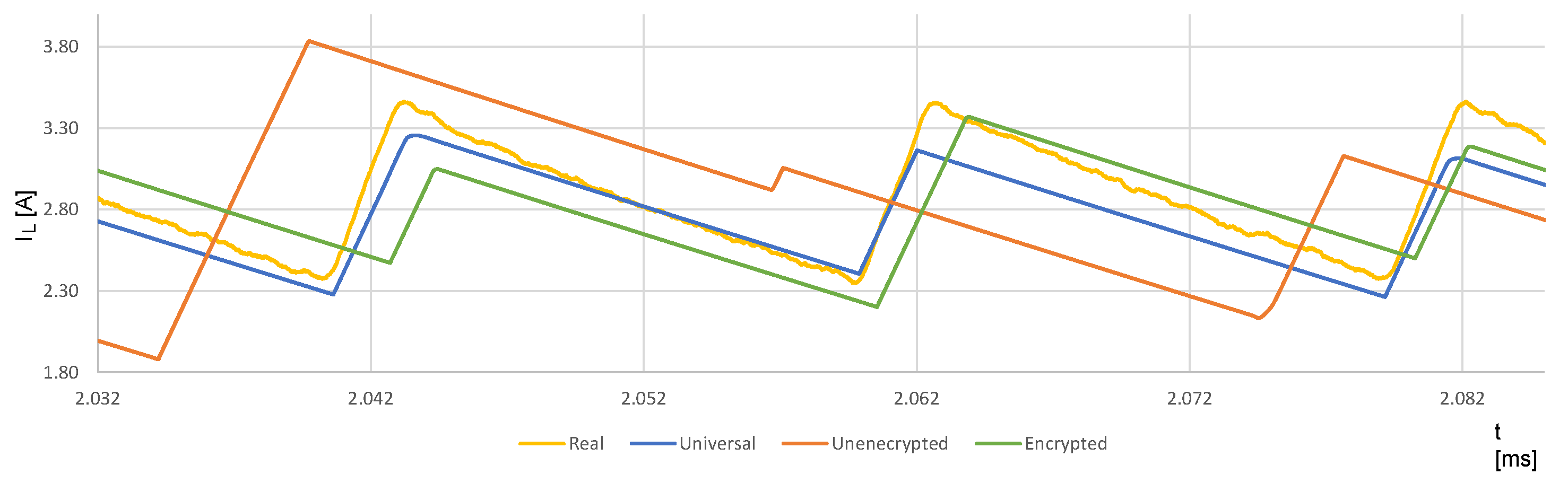
A comparison of the current course flowing through the coil
IL is shown in
Figure 18. The graph curves of universal, encrypted, and measured data are very close to each other with minimal differences.
Details of the coil current graph curves are shown in
Figure 19. As can be seen in
Figure 18 and
Figure 19, the curve of the coil current of the universal regulator model is much more similar to the real measurements and the encrypted model compared to the unencrypted model.
The last investigated steady-state parameter on the LM2576HV is the voltage on the load resistor (
VLoad). The time graph curves for the voltages on the load resistor are shown in
Figure 20. As can be seen from the figure, the voltages are very closer to each other. In order to demonstrate the differences in the models, a detailed view is presented in
Figure 21.
The most important parameters to observe are the frequency of the waveforms, voltage ripple (peak-to-peak), waveform shape, and value average. The phase shift between the signals is irrelevant from this point of view. The real measurement waveform is noisy, but it is possible to see the ripple and frequency of the signal when focusing on higher peaks. The average value of the load voltage between the waveforms difference is approximately 0.06 V only, where the universal model has the lowest average, 4.98 V, and the real measured values have the highest average at 5.04 V. The encrypted model average was 5.02 V, and the unencrypted model was 5.028 V. As can be seen from the detailed view, the ripple of other models is optically almost identical, especially when comparing the encrypted and the universal model. As mentioned above, the average load voltage value calculated from the universal model is the lowest, but the real differences are negligible.
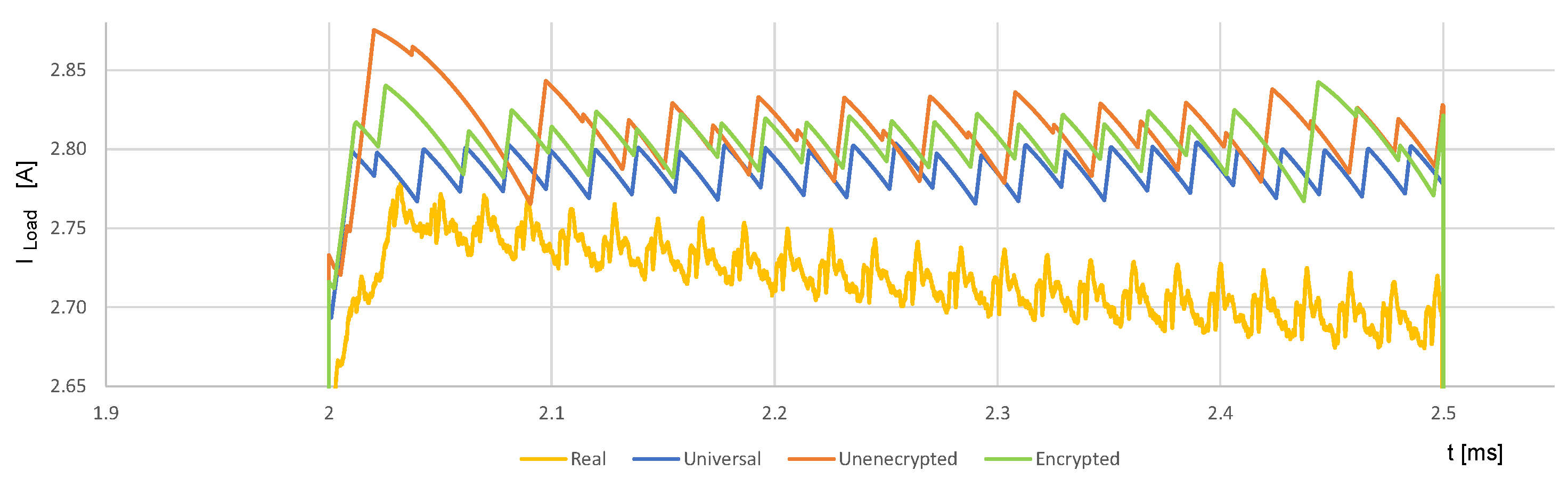
Next, the dynamic load behavior was investigated. The circuit was implemented according to
Figure 7, where the load R
L1 was the original 1.79Ω resistor and the second resistor was R
L2 = 37Ω. In the real measurement, the circuit switch was implemented by the SiC transistor UF3C065030T3S. The signal was generated by an Agilent 33500B Series Waveform Generator. The on-state switch time duration was 500μs. For the dynamic behavior, only the load voltage (
VLoad) and current (
ILoad) were investigated.
The V
Load response on the load change graph curves is shown in
Figure 22. The graph curves are again very close to each other; however, small differences can be seen in the figure. The differences are more obvious in the detailed view in
Figure 23.
The first obvious difference comparing simulations and real measurements is the voltage drop of the real DC–DC converter on the higher load. This voltage drop is caused by the parasitic resistance of the circuit elements, including joints and the electrical conductor. The measured value of the load resistance was
RL = 1.79Ω. This value already included parasite resistance, as mentioned above. This value is thus valid only for the specific load current. The voltage difference between the measured and simulated voltage at the low current is approximately 0.1 V (2%). The goal of the dynamic load state observation is to investigate the time response of the system and voltage ripple change. Moreover, the main goal of the research was to compare the universal model with the existing official models. For this reason, the voltage drop on the parasite resistance differences was not taken into account in the simulations. Another difference is the slightly lower V
Load value of the universal model compared to the official models and the real measurement. This behavior was already explored above in
Figure 21. In order to investigate the problem, Equation (4) was used to calculate the expected output, and the values of the real resistance were applied. The calculation result is in (5):
According to calculation (5), when applying the resistance values from the circuit and Vref from the datasheet, the regulated output voltage should be slightly under 5 V. According to this logic, the universal model is the closest to the calculated output voltage. The reason could be that the real converter settings calculate with a voltage drop-down on a higher load. Therefore, the voltage on a low load is a little bit higher. This voltage output shift is probably implemented in both official models. On the other hand, the measured VLoad during a high load is almost identical to the universal model simulation.
The current through the load
ILoad investigation is also very interesting. The
ILoad time graph curves are shown in
Figure 24 and in detail in
Figure 25.
The time graph curves show values very close to each other; however, a measured current drop-down can be observed. This behavior is more obvious in the detailed graph in
Figure 25.
The current dropdown of the measured course is caused by the Joule heating of the load. Increasing the temperature of the load resistor increases the value of the resistance and decreases the current when at a constant voltage. Other graph curves are very similar with negligible differences. The main complication in comparing simulations and real measurements is the value of the variable circuit—especially the temperature dependence of resistors. The temperature depends on the actual regulator load. The real circuits elements values were measured at room temperature (approx. 23 °C). This problem could be partially compensated by active cooling of the circuit.
The simulations and measurements above showed that if the 2576HV regulator’s parameters from the datasheet are applied in the universal model, it can be a full-fledged replacement for the official simulation models provided by the manufacturer. Moreover, the universal model is much closer to the encrypted model and measurement than the official unencrypted model. The unencrypted model shows good average values compared to the measuring, but a closer look at the time curves shows instability in the regulation process.
However, the universal model could have an advantage even over the official encrypted model. The datasheet [
11] refers to many parameters with a specific tolerance where the minimum, typical, and maximum value of the parameter is provided. Most of the parameters vary because of the temperature dependent. For instance, the oscillator frequency is typically 52 kHz, but the tolerance is in the range of 47–58 kHz. The current limit is typically 5.8 A, but the tolerance is in the range of 4.2–6.9 A. Feedback voltage is typically 1.23 but may vary in a range of 1.217–1.267 V. The official models most likely have typical values implemented. The universal model is capable of updating these parameters. When a real measurement is performed, the universal model can be tuned up for the specific regulator component in a specific situation (for instance, for higher temperatures, where typical parameter values cannot be guaranteed). In this situation, the universal model would be more precise compared to the official models.
4. Universal Model Comparison with the Official LM2594HV Model
In the third section, we proved that the universal model could be used as a full-fledged PSpice model replacement for the official LM2576HVmodel when parameters from the 2576HV datasheet [
26] were applied. A basic comparison to the LM2594HV official model [
26] was also made to prove the true universality. The main differences between the previous LM2576HV and LM2596 are that the LM2576 specified output current is 3 A, and it works on a 52 kHz frequency. The LM2594 has specified a 0.5 A output current and works on a 150 kHz frequency. The circuit components’ values were taken from the previous steady-state simulations—with the constant load to compare behavior with the previous simulation. The only difference in the circuit parameters was load resistor R
L = 10Ω to achieve the specified 0.5 A output and updated regulator parameters according to the LM2594HV datasheet [
28], as
Figure 26 shows.
In order to make the simulations more effective, previous parameters (
Isw,
Vreg-out,
IL,
VLoad) from the beginning time (t = 0) were observed. The simulations showed that the transient response takes approximately 10.8 ms, and after that, the regulator works on its work point. The reason for the longer time compared to the previous situation is the smaller maximum current of the regulator, and a longer time is required to fill the C2 capacitor (
Figure 4) with the desired voltage value. The next 60 µs of the simulation in the PSpice and the TINA were compared after the 11.5 ms.
First, regulator voltage output graph curves are shown in
Figure 27. The figure shows that the time graph curves are nearly identical.
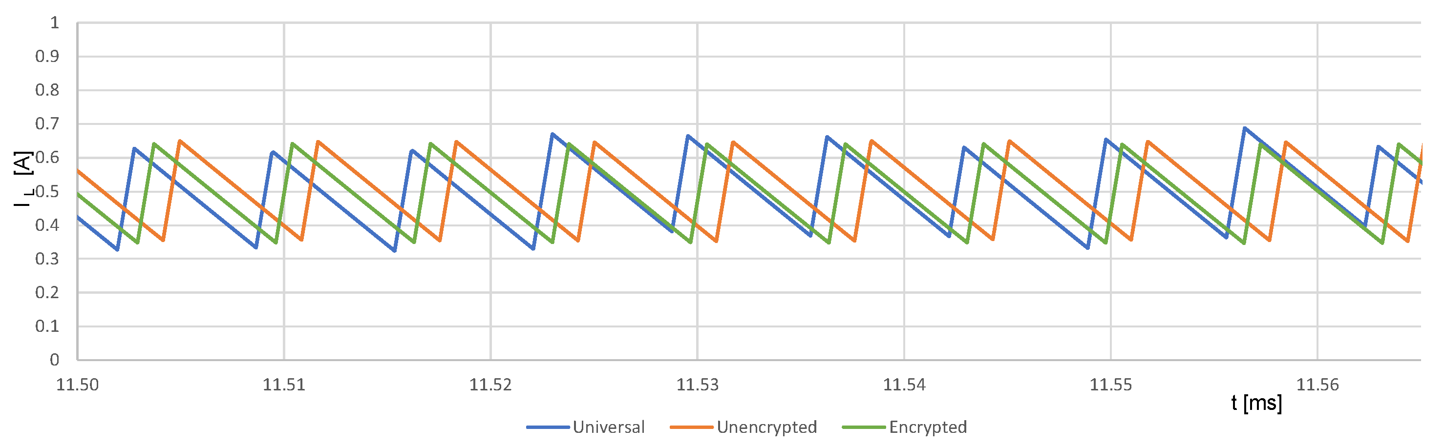
The current from the switching regulator
Isw is shown in
Figure 28. The figure shows that the time graph curves are similar in shape and frequency. The real difference is only peaks current and slightly increased maximum of the universal and unencrypted model compared to the encrypted model.
The current through the coil
IL time graph curves is shown in
Figure 29. The curves are again almost identical. The figures show that the officials and universal model results are very close to each other.
Finally, the resulting load voltage was compared. The differences are minimal, so a detailed view is presented in
Figure 30. The shape, frequency, and calculated load voltage ripple are almost identical. The difference between the official encrypted and the universal model is in absolute value, approximately 60 mV. The difference between the official unencrypted and the universal model is in absolute value, approximately 10 mV only. The universal model load voltage is higher compared to the official models. In the previous LM2576 simulations, this was the opposite. According to the datasheet, the LM2594 has an equal typical feedback voltage of 1.23 V; thus, Equation (5) can be applied. According to (5), the resulting load voltage was slightly below 5 V. Therefore, the universal model is again closer to the expected value.
As a result of comparing the simulations, we can confirm that the differences between the official LM2594 models encrypted, unencrypted, and the universal model after applying parameters from the datasheet are negligible. The unencrypted model for LM2594 seems more stable than the previous LM2576HV model.
5. Discussion
Some producers provide a PSpice module for their products, but generally, there is a limited number of switched voltage regulator PSpice models. All the existing models are only equivalents for specific switching regulator and their typical properties. The customization of such models is minimal. A circuit simulation using “similar” but not equal values can lead to erroneous results. When a switched voltage regulator is used in practice, where the regulator does not have an equivalent PSpice model, it is impossible to rely on simulations.
The proposed and tested universal PSpice model of a switched voltage regulator is fully customizable. It is built on the basic principles of the switching voltage regulators shown in
Figure 2 and allows any switching voltage regulator based on those principles to be simulated. It requires only the setup properties provided, usually from datasheets. Users do not have to depend on whether the manufacturer provides a PSpice model for their product to proceed with reliable simulations.
The paper aimed to present a universal PSpice model of the simple switcher such as LM2576, LM2596, LM 2577, etc. The buck DC–DC converter consists of a regulator switcher and other parts, where in addition to the switcher, the crucial are a coil and a capacitor as an output filter. The paper’s goal is not to design an optimal DC–DC buck converter with optimal values of the output filter parameters. The validation of the universal model is based on comparing the simulation results with other official models or real measurements under the same condition. Therefore, optimizing the output filter was not essential.
This paper showed that the universal model could be used as a full-fledged replacement for official simple regulator switcher simulation models of buck DC–DC converters. The simulation shows that the encrypted model has better and more stable results than the unencrypted model in the case of the LM2576HV model. The universal model shows results very close to the encrypted model. The only differences could be observed in the final voltage on the load, but according to the datasheet, the universal model is mathematically closer to the expected value.
A comparison with two different DC–DC regulators, LM2576 and LM2594, was performed. The LM2576 regulator was also compared with the real measurements and a dynamic load transient analysis. The presented universal PSpice model of a switched voltage regulator shows a very close match with the official model and also with the practically measured waveforms, even when it is adapted to various regulators. Generally, it cannot be claimed that the universal model is more accurate than the encrypted model provided by the manufacturers. Nevertheless, we can claim that the universal model is generally accurate level to the official encrypted models. It means that the universal model can be used as a simulation model in the TINA simulation software for the regulators, where only an encrypted model is provided or no official model exists at all. The universal model accuracy with the real regulator can be increased when the measurement of the element is performed. Then, the accurate parameters of the model could be calculated from the measurements. It would allow the user to simulate the regulator in different circumstances more accurately than the official models with constant parameters.
A significant advantage of our proposed model is that our model behavior could be more closely to real behavior when compared to official simulation models in a different situation. An example of such a situation could be, for instance, a simple parallel connection of the regulators. Equal current sharing can be observed when using official models, which is very unlikely, and it would be true only if the real regulator parameters were to be completely equal. However, slight parameter variation given by the manufacturer’s tolerance is typically present between the different items of the same switching regulator type. These slight parameter differences could be set, or the parameter delay can be used using the universal model. It allows individual components to be customized if used multiple times in one circuit connection, and behavior can be more closely observed in a real situation.


 ,
, 


