Abstract
Solar photovoltaic energy is the most prominent candidate to speed up the transition from the existing non-renewable energy system to a more efficient and environmentally friendly one. Currently, silicon cells dominate the photovoltaic market owing to their cost-effectiveness and high efficiency, nowadays approaching the theoretical limit. Higher efficiency can be achieved by tandem devices, where a wide bandgap semiconductor is stacked on top of the silicon cell. Thin-film perovskite technology has emerged as one of the most promising for the development of silicon-based tandems because of the optimal perovskite opto-electronic properties and the fast progress achieved in the last decade. While most of the reported perovskite/silicon tandem devices exploit a two-terminal series connected structure, three-terminal solutions have recently drawn significant attention due to their potential for higher energy yield. In this work, we report for the first time a theoretical study, based on validated optical and electrical simulations, of three-terminal perovskite/silicon solar cells employing a hetero-junction bipolar transistor structure. With respect to other three-terminal tandems proposed so far, the transistor structure can be implemented with rear-contact silicon cells, which are simpler and more common than interdigitated back-contact ones.
1. Introduction
The demand for renewable energy is growing rapidly. Photovoltaics (PV) can provide clean energy at a low cost and is expected to be the main source of energy in the future [1]. Silicon solar cells are the most common PV technology, with a market share of 90%. They are largely based on cost-effective technologies such as p-type Back-Surface-Field (BSF) or Passivated-Emitter and Rear-Cell (PERC) that provide an efficiency of about 20–25%. This value is outperformed by the emerging Si heterojunction (HTJ) solar cell technology, which achieves a record efficiency of 27.6% [2]. A way to overcome these values is to use a tandem structure that increases the theoretical efficiency from 30% to 42% [3] by adding a wide bandgap semiconductor on top of a Si solar cell.
Organometal halide perovskite (PVK) materials are ideal candidates for the development of low-cost thin-film tandems owing to their optimal properties such as high absorbance, ambipolar transport, defect tolerance, low-temperature processing, chemical and band tunability [4,5]. Among thin-film tandem technologies, PVK/Si tandems seem to be one of the most promising routes to market according to the International Technology Roadmap for Photovoltaics and have already surpassed efficiency of 31% [6]. To make them commercially viable, extensive research is carried out worldwide not only to demonstrate high efficiency but also cope with the issues of large area scaling [7,8] and stability of the perovskite cell that can be tackled with an holistic approach [8] by stabilizing the perovskite layer itself [9] as well as the charge transport layer [10].
PVK solar cells can be combined with Si to realize tandem cells with 2, 3 and 4 terminals (2T, 3T and 4T in Figure 1) [11,12]. In 2T tandems (Figure 1a), the cells are monolithically fabricated on top of each other and connected in series through an interconnection layer realized by a poly- or amorphous-silicon tunnel junction or by a recombination layer usually made by a transparent conducting oxide (TCO). The interconnection layer induces optical losses, lowering the achievable efficiency [13] and, when realized with highly conductive layers, may facilitate electrical shunting and prevent upscaling to large areas [12,14]. In 4T tandems (Figure 1b), the cells are mechanically stacked, and the electrical power is extracted independently at each cell. This removes the current matching constraint required by the 2T design at the price of higher optical losses, because additional transparent layers are needed as well as higher fabrication cost.

Figure 1.
Scheme of PVK/Si tandem solar cells with 2 terminal (a), 4 terminal (b) and 3 terminal (c) configuration.
An alternative, less explored, solution is provided by the 3T design that aims at combining the advantages of 2T and 4T tandems. It retains the monolithic structure of the 2T one, but a third contact is introduced at the recombination layer. This allows for the independent operation of the two sub-cells and removes the current mismatch loss of 2T devices [15,16,17]. The slightly higher fabrication cost might be compensated by the material flexibility (looser requirements on bandgap) and higher energy yield in real-word operation, owing to higher resilience to spectral and temperature variations [17,18,19,20,21].
A lot of research has emerged on the development of 3T III-V/Si tandems [15] using interdigitated back contact (IBC) Si-HTJ cells (Figure 1c). Tockhorn et al. have recently reported an experimental proof-of-concept 3T PVK/Si cell based on interdigitated back contact silicon [22] (see Figure 1) with efficiency of 17.1%, and a potential to reach about 27%. On the other hand, the development of 3T PVK/Si tandems on rear-contact Si cells is an alternative attractive route, albeit less studied, due to the widespread use of these last in the marketplace.
In this direction, one promising solution is provided by the 3T Heterojunction Bipolar Transistor (3T-HBT) solar cell concept proposed by Martì and Luque [23]. The idea is to realize a tandem cell whose top and bottom sub-cells are made by the emitter–base and base–collector (hetero) junctions of a bipolar transistor [24]. The common base layer provides the electrical and optical connection between the two sub-cells, avoiding the need for any tunnel junction or recombination layer, and it is used to realize the third terminal contact layer. Theoretically, the 3T-HBT solar cell achieves the same efficiency as the 2T double junction cell. Very promising experimental results have been reported for devices made on III–V semiconductors [25,26].
In this work, we study for the first time the feasibility of three-terminal PVK/Si tandems using the heterostructure bipolar architecture. To this aim, starting by a 2T PVK/Si tandem inspired from previous experimental devices reported in literature [27,28], we identify a possible implementation of a 3T-HBT tandem. Then, based on coupled electromagnetic and transport simulations previously validated against experimental data [29], we carry out a thorough analysis of its photovoltaic behavior compared to the 2T cell.
2. Structure and Operating Principle of the PVK/Si 3T-HBT Tandem
Figure 2a presents a schematic drawing of a PVK/Si 3T-HBT tandem made of a n-i-p perovskite solar cell (PSC) on top of a heterojunction with an intrinsic thin-layer (HIT) bottom cell on p-type c-Si. The hole transport layer (HTL) and the PVK form the HBT emitter; the electron transport layer (ETL) and the amorphous hydrogenated Si layers (a-Si:H) form the base; finally, the p-type c-Si acts as the HBT collector. The device exploits a Top Interdigitated Contact (TIC) scheme for the emitter and base terminals [30]. The three contacts for emitter, base, and collector are named as T, Z, and R, respectively, following the notation in [30].
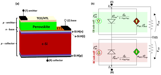
Figure 2.
(a) Three-dimensional (3D) schematic view of a 3T-HBT PVK/HIT-silicon tandem with top interdigitated contact scheme. The three contacts for emitter, base, and collector are named as T, Z, and R, respectively. (b) Equivalent electrical circuit of the p-n-p 3T-HBT solar cell sketched on the left under illumination.
Figure 2b shows the equivalent electrical circuit of the HBT tandem. The top emitter–base (EB) and bottom base–collector (BC) junctions form two back-to-back connected solar cells with their separate loads. Thus, under illumination, the total electrical power generated by the tandem is the sum of the electrical powers provided to the loads across the T-Z and Z-R terminals. By that, the bipolar structure not only works as a double junction (DJ) solar cell without the need of any recombination layer or tunnel junction but also solves the current matching constraint of series-connected DJ cells.
For the feasibility of the HBT tandem, it is critical to verify that the common base layer does not negatively affect the PV conversion efficiency achievable by the two sub-cells. In Figure 2b, the equivalent circuit of the EB (BC) sub-cell is made by three components: a photogenerated current generator () in parallel to a diode with reverse saturation current () as in classical solar cells, and, added to these, a current-controlled current source (). This last one accounts for the effect of the BC voltage on the EB junction due to the injection of minority carriers from the collector to the emitter (and vice versa) through the common base layer. The coefficients , model this electrical coupling, the so-called transistor effect, whose strength depends on a few physical device parameters, such as doping levels, energy band discontinuities and minority carrier diffusion length at the BE and BC junctions. As well known from bipolar transistor theory [24], the closer () gets to 1, the stronger the transistor effect is. To understand the repercussion of the transistor effect on the photovoltaic conversion efficiency, we shall notice that it induces an increased dark current of the sub-cells: in fact, the reverse saturation current of the diodes in Figure 2b is equal to the value expected for the corresponding isolated junction (, ) amplified by the factor . By that, the transistor effect causes a reduction of the attainable open circuit voltage of each sub-cell and a reduction of the maximum achievable power conversion efficiency. Therefore, from the perspective of photovoltaic operation, the transistor action shall be minimized [31,32].
3. Methods
3.1. Device under Study
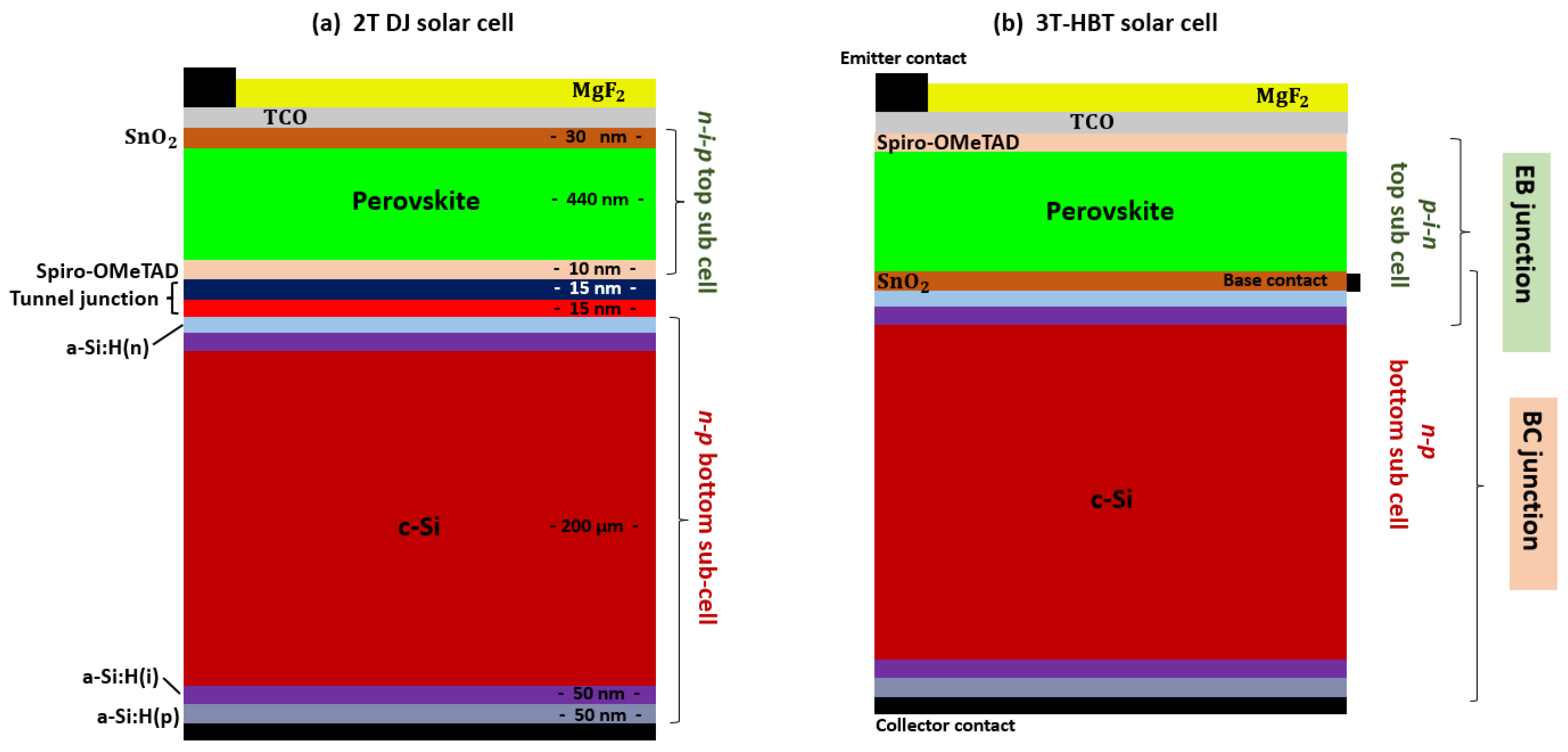
Figure 3 sketches the devices studied and simulated in this work. The 2T DJ solar cell stacks an n-i-p PVK solar cell on top of an n-p Si HIT bottom cell. The PVK and HIT sub-cells are connected through a / Si tunnel junction (Figure 3a). The PVK sub-cell consists of a 440 nm perovskite absorbing layer [33,34] sandwiched between a 30 nm thick SnO ETL [35,36] and a 10 nm thick Spiro-OMeTAD HTL [33,35]. The HIT sub-cell consists of 200 μm p-doped c-Si sandwiched by two thin films of hydrogenated amorphous silicon (a-Si:H) from the top (bottom) 50 nm of n- (p-)doped a-Si:H and 50 nm of intrinsic a-Si:H. In the simulations, we assume a 107 nm thick MgF anti-reflection layer and fully transparent TCO layer. The choice of ETL and HTL materials used in this study was inspired by previous literature studies [27,28,37]. Different choices may be possible, also for the PVK layer, but they will not significantly affect the main conclusions that can be drawn from the comparative analysis proposed in this work between the conventional 2T double junction device and the 3T-HBT one.
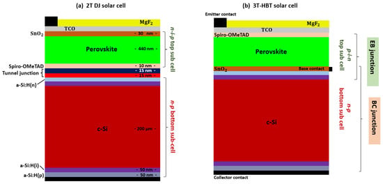
Figure 3.
Schematic view of the simulated PVK/HIT-silicon tandems with (a) 2T DJ structure and (b) 3T-HBT structure.
From a conceptual point of view, the 3T-HBT solar cell structure in Figure 3b can be obtained through the following modifications of the DJ cell: removing the tunnel junction, flipping the n-i-p PSC and implementing the third lateral contact at the SnO layer. In a typical fabrication flow, SnO would be deposited directly over the a-Si:H layer by solution processing: for instance, by using the colloidal dispersion of nanoparticles [38]. In case of textured substrates, conformal deposition could be based on chemical bath deposition as well as sputtering [39,40]. The perovskite layer can be deposited either by solution processing or by thermal evaporation [41]. The same type of wet or vacuum deposition can also be used for the Spiro-OMeTAD [38]. The transparent electrode can be deposited by the sputtering of indium tin oxide, which is followed by the deposition of the antireflection layer of MgF [42]. Finally, two metal grids can be deposited on the emitter and base contacts after a laser ablation step to remove the MgF or the entire PSC stack, respectively.
The resulting device sketched in Figure 3b consists of: Spiro-OMeTAD and PVK layers to form the region, SnO and (n)-(i) a-Si:H layers to form the region, and finally, c-Si and (i)-(p) a-Si:H layers to form the region. Thus, one obtains a tandem with two sub-cells made by the p-i-n EB and the n-p BC junctions.
3.2. Simulation Approach and Material Models
Physics-based simulations were carried out with the Sentaurus Technology Computer-Aided Design (TCAD) software from Synopsys [43]. The optical carrier generation profile is calculated using the Transfer Matrix Method (TMM) and given as an input to the classical Poisson drift diffusion (DD) transport model. The simulations assume illumination under AM1.5G spectrum (total power of ≈100 mW/cm) at normal incidence.
Perovskite, ETL and HTL materials are modeled as classical crystalline semiconductors, following previous work in the literature [33,35,44,45]. Metal halide perovskite materials have a tunable direct bandgap ranging from ∼1.24 eV (FASnI) up to ∼3.55 eV (FASnCl) [46] based on their composition, i.e., Cesium (Cs), formamidinium (FA) and/or methylammoinium (MA) for the cation, Pb and/or Sn for the metal and I, Cl, Br for the halide. In this work, we exploit the most widely used methylammonium lead triiodide with eV, covering the entire visible region ( nm) [35]. Spiro-OMeTAD and SnO band parameters were also taken from [35].
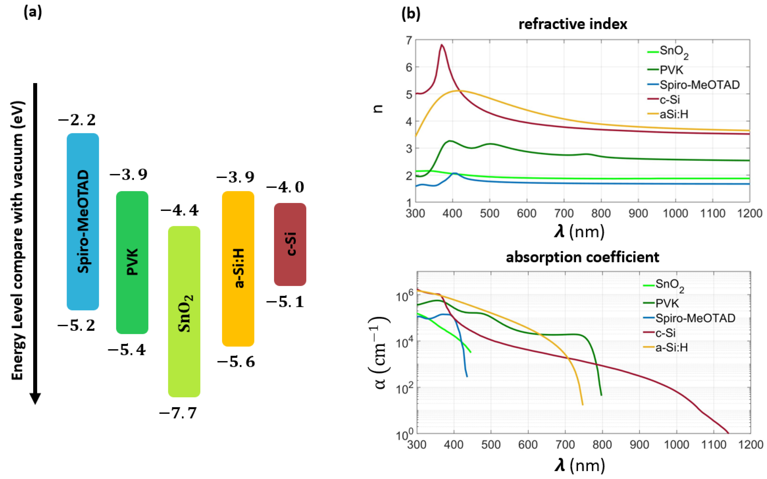
Figure 4 reports a schematic representation of the assumed band alignment between the different materials and the wavelength-dependent refractive index and absorption coefficient used in the optical simulations (the complex refractive index data are available at [47]). Table 1 summarizes the main electrical material parameters and doping levels. Simulations include radiative recombination only, with the radiative recombination coefficient set to cm/s [48] for all the PVK sub-cell materials, cm/s for a-Si:H [34] and cm/s for c-Si [43]. The simulation methodology was previously validated against experimental data in [29].
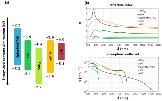
Figure 4.
(a) Schematic representation of band structure and energy levels of various materials used in the pervovskite/silicon tandem analyzed in our study. (b) Real part of the refractive index (top) and wavelength-dependent absorption coefficient (bottom) for the materials used in the PVK and HIT sub-cells.

Table 1.
Main parameters value. : Bandgap : Electron affinity : Permittivity : Density of states μ: Mobility : Lifetime. (e/h): electron/hole; if not specified, the shown value is the same for both carriers.
Figure 5 shows the energy band diagram under thermal equilibrium condition for the double junction and HBT solar cells. The flipping of the PVK top cell and the presence of the tunnel junction made by highly doped (5 ×∼) silicon in the DJ structure are well visible.
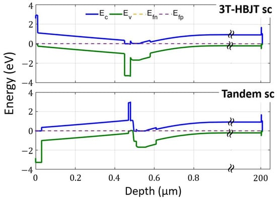
Figure 5.
Energy band diagram of the 3T-HBT (top) and DJ (bottom) tandems under thermal equilibrium condition.
4. Results
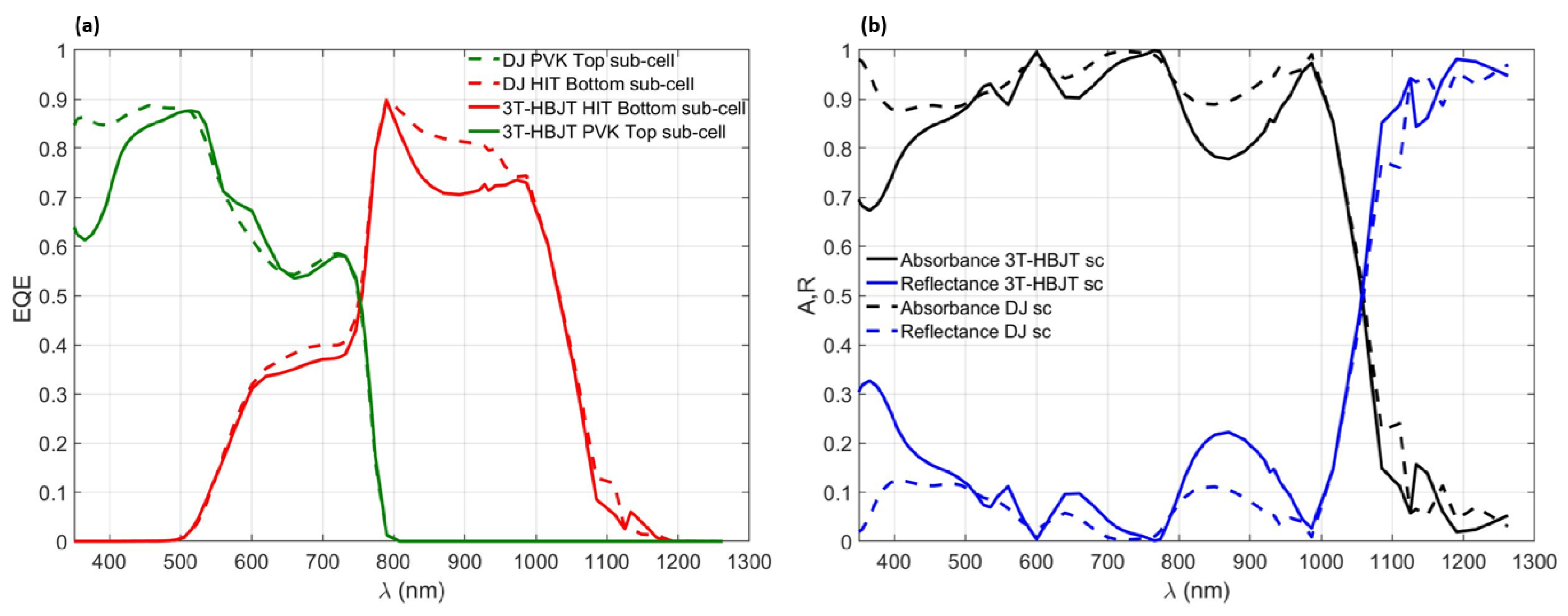
At first, we have analyzed the spectral response of the DJ and 3T-HBT devices. As seen in Figure 6a, the External Quantum Efficiency (EQE) of the 3T-HBTSC, based on the n-i-p PVK top sub-cell architecture, shows a slight EQE penalty at low wavelength (<500 nm) and in the silicon harvesting range (800–1000 nm range), due to the increased reflectance (Figure 6b) in those wavelength ranges.
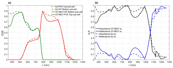
Figure 6.
(a) External Quantum Efficiency and (b) Absorbance and Reflectance for the 3T-HBT (solid line) and 2T-DJ (dashed lines) solar cells.
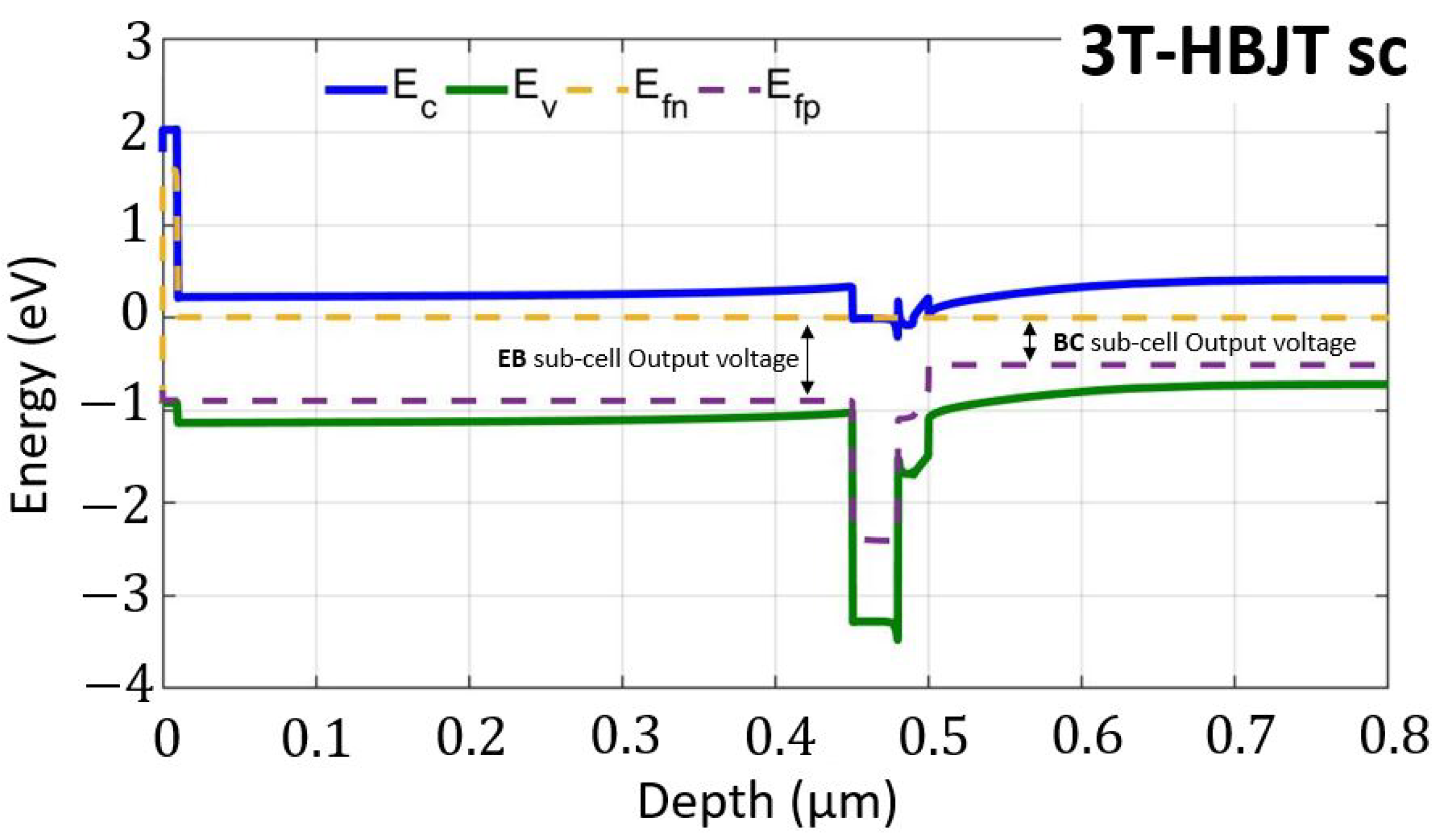
This can be explained by the flipping of the PVK top cell in the HBT tandem with respect to the DJ one, which brings at the cell illumination face the Spiro-OMeTAD layer, whose refractive index is higher than that one of the SnO layer [49]. However, this optical penalty could be avoided by flipping the bottom silicon sub-cell, instead of the top one, to obtain an n-p-n 3T-HBT solar cell [29]. Indeed, in this case, the solar cell will be illuminated by the n-side (SnO layer), the Spiro-OMeTAD layer being below the PVK one, analogously to the 2T DJ solar cell in Figure 3, thus preventing the spectral loss induced by the Spiro-OMeTAD layer in the HBT under study, as we have shown in [29]. Moreover, for the sake of the following discussion, we notice that the penalty in the EQE of the HIT cell turns to be almost irrelevant in terms of the comparative performance of the HBT and DJ tandems, because the current in the DJ tandem is limited by the top cell. As discussed in Section 2, in the 3T-HBTSC, in principle, the EB and BC junctions influence each other owing to the common base layer. To assess the impact of this mechanism on the photovoltaic performance, we have simulated the current–voltage characteristic of each sub-cell, taking into account the operating condition of the other one. Figure 7 reports three contour maps, showing how the efficiency of the two sub-cells and of the entire device changes as a function of the voltages and . It can be observed that the efficiency of each sub-cell varies with its own bias and is practically independent on the operating voltage of the other one. Therefore, the maximum power point (MPP) of the tandem corresponds to the MPP of the two sub-cells working as if they were independent. In other words, there is no cross-talk between the two junctions, which is in line with the experimental findings in [31] for a 3T-HBT fabricated on III–V compound semiconductors. This demonstrates the robustness of the HBT solar cell architecture regardless of the particular material system. In fact, the energy bandgap difference between the top and bottom sub-cells, which is an inherent characteristic of tandem solar cells, ensures a negligible injection of carriers from the collector toward the emitter, i.e., a small coupling coefficient and a marginal increase of the dark current of the two sub-cells. Therefore, the two sub-cells develop an open circuit voltage comparable to that achievable as stand-alone cells. This is reflected in the energy band diagram under MPP operating condition shown in Figure 8. Here, the different splitting of the quasi-Fermi levels in the PVK and HIT sub-cells is well visible: indeed, the hole quasi-Fermi level bends in the base region so that the voltage of the top cell is not limited by the low gap of the HIT cell [31].
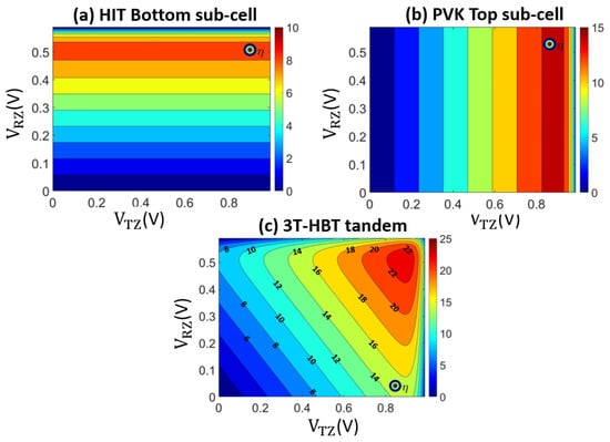
Figure 7.
(a) Efficiency as a function of the TZ and RZ voltages for: (a) HIT bottom sub-cell; (b) PVK bottom sub-cell; (c) 3T-HBT tandem.
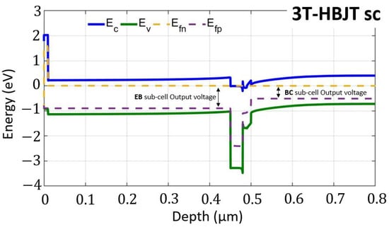
Figure 8.
Energy band diagram of the p-n-p 3T-HBT (Figure 3) with each junction biased at maximum power point. The dashed yellow and pink lines are the electron and hole quasi-Fermi levels, respectively.
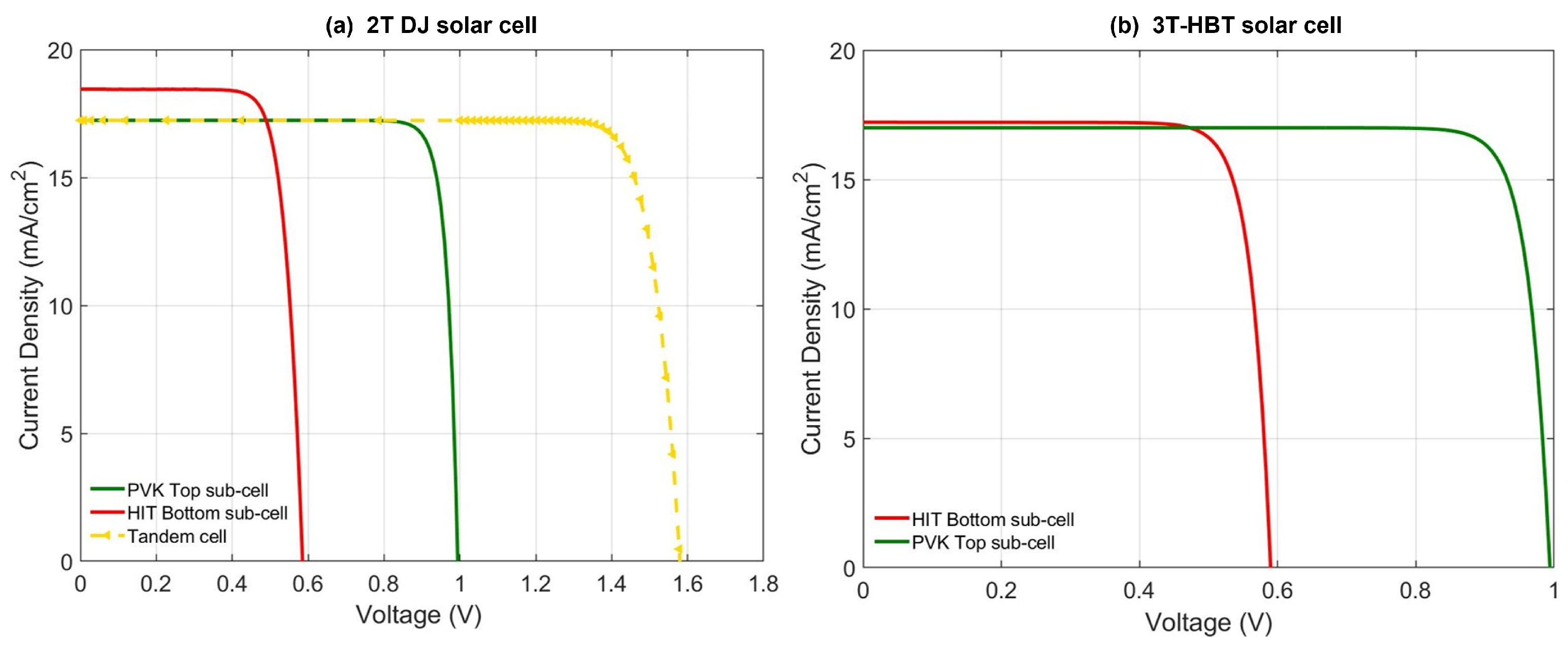
Finally, Figure 9 shows the simulated J-V characteristics of the 2T-DJ and of the 3T-HBT tandems, and Table 2 summarizes their photovoltaic figures of merit. At short circuit, we can observe that the bottom cell provides a higher current in the 2T-DJ structure than in the 3T-HBT one, which is due to the above-mentioned penalty in the EQE. This difference, however, does not affect the tandem efficiency, because the short circuit current of the DJ tandem is limited by the top cell due to the current matching constraint. The open circuit voltages are comparable in the two devices, with a difference of the order of a few tens of mV. Overall, our analysis of the 3T-HBT and DJ tandems, based on realistic material parameters and device model, shows that they attain comparable efficiency as expected according to more idealized detailed balance models [23]. The proof-of-concept devices in this work demonstrate an efficiency of 23% that can be further improved by design optimization as shown in [22,29].
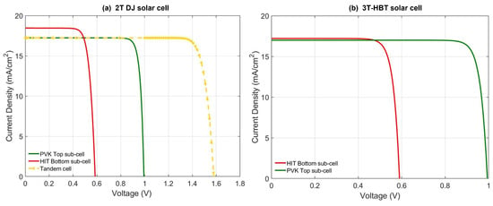
Figure 9.
(a) J-V characteristics of the flat 2T PVK/Si DJ solar cell; (b) J-V characteristics of the flat 2T PVK/Si 3T-HBT solar cell.

Table 2.
3T-HBT and DJ solar cells: Figures of merit.
5. Conclusions
We have presented a numerical study of perovskite/silicon three-terminal tandems based on the heterojunction bipolar transistor architecture to investigate their potential, and possible bottlenecks, with respect to more conventional two-terminal double junction tandems. Starting from a representative 2T series-connected PVK/HIT-Si tandem inspired to recently reported devices, it is shown that a p-n-p HBT structure could be realized by removing the tunnel junction and flipping the PVK cell. This creates two back-to-back cells with a common layer, the n-base, that is used to extract the third contact. Optical and transport simulations show that the direct electrical coupling between the top and bottom sub-cells does not induce any significant power loss, and therefore, the HBT tandem achieves almost the same efficiency as the DJ one, avoiding the use of any tunnel junction or recombination layer. This, added to the relaxation of the current matching condition, demonstrates that the HBT architecture could be a promising route toward the development of 3T PVK-Si tandems based on rear-contact silicon technologies. The presented device is developed within an HIT-Si platform, but it is also compatible with homojunction silicon technologies. Further studies will be needed to cope with the challenge of designing proper contact grids aimed at minimizing parasitic effects associated to the lateral base resistance and increased shadow loss due to the added contact and to put this novel tandem concept in practice by developing an appropriate fabrication process.
Author Contributions
Conceptualization, G.G., F.C. and F.D.G.; methodology, G.G. and F.C.; software, G.G.; validation, G.G., F.C.; resources, F.C.; data curation, G.G.; writing—original draft preparation, G.G.; writing—review and editing, G.G., F.C. and F.D.G.; visualization, G.G.; supervision, F.C.; project administration, F.C.; funding acquisition, F.C. All authors have read and agreed to the published version of the manuscript.
Funding
This research was partly funded by the ECSEL Joint Undertaking (JU) under grant agreement No. 101007247. The JU receives support from the European Union’s Horizon 2020 research and innovation programme and Finland, Austria, Germany, Ireland, Iceland, Italy, Sweden, and Switzerland.
Data Availability Statement
The material data used in this study are openly available in Zenodo at https://doi.org/10.5281/zenodo.7116993, accessed on 27 September 2022.
Conflicts of Interest
The authors declare no conflict of interest. The funders had no role in the design of the study; in the collection, analyses, or interpretation of data; in the writing of the manuscript, or in the decision to publish the results.
References
- International Technology Roadmap for Photovoltaic (ITRPV), 11th ed.; 2020; Available online: https://resources.solarbusinesshub.com/solar-industry-reports/item/international-technology-roadmap-for-photovoltaic-itrpv-2019 (accessed on 1 September 2022).
- Green, M.; Dunlop, E.; Hohl-Ebinger, J.; Yoshita, M.; Kopidakis, N.; Hao, X. 3 Solar cell efficiency tables (version 57). Prog. Photovolt. Res. Appl. 2021, 29, 3–15. [Google Scholar] [CrossRef]
- De Vos, A. Detailed balance limit of the efficiency of tandem solar cells. J. Phys. D Appl. Phys. 1980, 13, 839. [Google Scholar] [CrossRef]
- Lal, N.N.; Dkhissi, Y.; Li, W.; Hou, Q.; Cheng, Y.B.; Bach, U. Perovskite Tandem Solar Cells. Adv. Energy Mater. 2017, 7, 1602761. [Google Scholar] [CrossRef]
- Fu, F.; Li, J.; Yang, T.C.J.; Liang, H.; Faes, A.; Jeangros, Q.; Ballif, C.; Hou, Y. Monolithic Perovskite-Silicon Tandem Solar Cells: From the Lab to Fab? Adv. Mater. 2022, 34, 2106540. [Google Scholar] [CrossRef] [PubMed]
- NREL. Best Research-Cell Efficiencies: Emerging Photovoltaics. 2022. Available online: https://www.nrel.gov/pv/assets/pdfs/cell-pv-eff-emergingpv-rev220630.pdf (accessed on 1 September 2022).
- Lee, D.K.; Park, N.G. Materials and Methods for High-Efficiency Perovskite Solar Modules. Sol. RRL 2022, 6, 2100455. [Google Scholar] [CrossRef]
- Reddy, S.H.; Di Giacomo, F.; Di Carlo, A. Low-Temperature-Processed Stable Perovskite Solar Cells and Modules: A Comprehensive Review. Adv. Energy Mater. 2022, 12, 2103534. [Google Scholar] [CrossRef]
- Huang, J.; He, S.; Zhang, W.; Saparbaev, A.; Wang, Y.; Gao, Y.; Shang, L.; Dong, G.; Nurumbetova, L.; Yue, G.; et al. Efficient and Stable All-Inorganic CsPbIBr2 Perovskite Solar Cells Enabled by Dynamic Vacuum-Assisted Low-Temperature Engineering. Sol. RRL 2022, 6, 2100839. [Google Scholar] [CrossRef]
- Wang, T.; Zhang, Y.; Kong, W.; Qiao, L.; Peng, B.; Shen, Z.; Han, Q.; Chen, H.; Yuan, Z.; Zheng, R.; et al. Transporting holes stably under iodide invasion in efficient perovskite solar cells. Science 2022, 377, 1227–1232. [Google Scholar] [CrossRef]
- Futscher, M.H.; Ehrler, B. Efficiency Limit of Perovskite/Si Tandem Solar Cells. ACS Energy Lett. 2016, 1, 863–868. [Google Scholar] [CrossRef]
- Leijtens, T.; Bush, K.A.; Prasanna, R.; McGehee, M.D. Opportunities and challenges for tandem solar cells using metal halide perovskite semiconductors. Nat. Energy 2018, 3, 828–838. [Google Scholar] [CrossRef]
- Messmer, C.; Goraya, B.S.; Nold, S.; Schulze, P.S.; Sittinger, V.; Schön, J.; Goldschmidt, J.C.; Bivour, M.; Glunz, S.W.; Hermle, M. The race for the best silicon bottom cell: Efficiency and cost evaluation of perovskite–silicon tandem solar cells. Prog. Photovolt. Res. Appl. 2021, 29, 744–759. [Google Scholar] [CrossRef]
- Sahli, F.; Kamino, B.A.; Werner, J.; Bräuninger, M.; Paviet-Salomon, B.; Barraud, L.; Monnard, R.; Seif, J.P.; Tomasi, A.; Jeangros, Q.; et al. Improved Optics in Monolithic Perovskite/Silicon Tandem Solar Cells with a Nanocrystalline Silicon Recombination Junction. Adv. Energy Mater. 2018, 8, 1701609. [Google Scholar] [CrossRef]
- Warren, E.L.; Deceglie, M.G.; Rienäcker, M.; Peibst, R.; Tamboli, A.C.; Stradins, P. Maximizing tandem solar cell power extraction using a three-terminal design. Sustain. Energy Fuels 2018, 2, 1141–1147. [Google Scholar] [CrossRef]
- Park, I.J.; Park, J.H.; Ji, S.G.; Park, M.A.; Jang, J.H.; Kim, J.Y. A three-terminal monolithic perovskite/Si tandem solar cell characterization platform. Joule 2019, 3, 807–818. [Google Scholar] [CrossRef]
- Gota, F.; Langenhorst, M.; Schmager, R.; Lehr, J.; Paetzold, U.W. Energy yield advantages of three-terminal perovskite-silicon tandem photovoltaics. Joule 2020, 4, 2387–2403. [Google Scholar] [CrossRef]
- Schulte-Huxel, H.; Friedman, D.J.; Tamboli, A.C. String-level modeling of two, three, and four terminal Si-based tandem modules. IEEE J. Photovolt. 2018, 8, 1370–1375. [Google Scholar] [CrossRef]
- Filipič, M.; Löper, P.; Niesen, B.; Wolf, S.D.; Krč, J.; Ballif, C.; Topič, M. CH3NH3PbI3 perovskite / silicon tandem solar cells: Characterization based optical simulations. Opt. Express 2015, 23, A263–A278. [Google Scholar] [CrossRef]
- Santbergen, R.; Uzu, H.; Yamamoto, K.; Zeman, M. Optimization of Three-Terminal Perovskite/Silicon Tandem Solar Cells. IEEE J. Photovolt. 2019, 9, 446–451. [Google Scholar] [CrossRef]
- Akhil, S.; Akash, S.; Pasha, A.; Kulkarni, B.; Jalalah, M.; Alsaiari, M.A.; Harraz, F.A.; Balakrishna, R.G. Review on perovskite silicon tandem solar cells: Status and prospects 2T, 3T and 4T for real world conditions. Mater. Des. 2021, 211, 110138. [Google Scholar] [CrossRef]
- Tockhorn, P.; Wagner, P.; Kegelmann, L.; Stang, J.C.; Mews, M.; Albrecht, S.; Korte, L. Three-terminal perovskite/silicon tandem solar cells with top and interdigitated rear contacts. ACS Appl. Energy Mater. 2020, 3, 1381–1392. [Google Scholar] [CrossRef]
- Martí, A.; Luque, A. Three-terminal heterojunction bipolar transistor solar cell for high-efficiency photovoltaic conversion. Nat. Commun. 2015, 6, 1–6. [Google Scholar] [CrossRef] [PubMed]
- Sze, S.M.; Ng, K.K. Bipolar Transistors. In Physics of Semiconductor Devices; John Wiley & Sons, Ltd.: Hoboken, NJ, USA, 2006; pp. 241–292. [Google Scholar] [CrossRef]
- Zehender, M.H.; García, I.; Svatek, S.A.; Steiner, M.A.; García-Linares, P.; Warren, E.; Tamboli, A.; Martí, A.; Antolín, E. Demonstrating the GaInP/GaAs Three-Terminal Heterojunction Bipolar Transistor Solar Cell. In Proceedings of the 2019 IEEE 46th Photovoltaic Specialists Conference (PVSC), Chicago, IL, USA, 16–21 June 2019; pp. 35–40. [Google Scholar] [CrossRef]
- Antolín, E.; Zehender, M.H.; Svatek, S.A.; García-Linares, P.; Martí, A. III-V-on-silicon triple-junction based on the heterojunction bipolar transistor solar cell concept. In Proceedings of the 2020 47th IEEE Photovoltaic Specialists Conference (PVSC), Calgary, AB, Canada, 15 June–1 August 2020; pp. 1226–1231. [Google Scholar] [CrossRef]
- Sahli, F.; Werner, J.; Kamino, B.A.; Bräuninger, M.; Monnard, R.; Paviet-Salomon, B.; Barraud, L.; Ding, L.; Diaz Leon, J.J.; Sacchetto, D.; et al. Fully textured monolithic perovskite/silicon tandem solar cells with 25.2% power conversion efficiency. Nat. Mater. 2018, 17, 820–826. [Google Scholar] [CrossRef] [PubMed]
- Rombach, F.M.; Haque, S.A.; Macdonald, T.J. Lessons learned from spiro-OMeTAD and PTAA in perovskite solar cells. Energy Environ. Sci. 2021, 14, 5161–5190. [Google Scholar] [CrossRef]
- Giliberti, G.; Cappelluti, F. Physical simulation of perovskite/silicon three-terminal tandems based on bipolar transistor structure. In Physics, Simulation, and Photonic Engineering of Photovoltaic Devices XI, Proceedings of the International Society for Optics and Photonics, SPIE, San Francisco, CA, USA, 22 January–28 February 2022; Freundlich, A., Collin, S., Hinzer, K., Eds.; SPIE OPTO: San Francisco, CA, USA, 2022; Volume 11996, p. 1199602. [Google Scholar] [CrossRef]
- Warren, E.L.; McMahon, W.E.; Rienäcker, M.; VanSant, K.T.; Whitehead, R.C.; Peibst, R.; Tamboli, A.C. A Taxonomy for Three-Terminal Tandem Solar Cells. ACS Energy Lett. 2020, 5, 1233–1242. [Google Scholar] [CrossRef]
- Antolín, E.; Zehender, M.H.; Svatek, S.A.; Steiner, M.A.; Martínez, M.; García, I.; García-Linares, P.; Warren, E.L.; Tamboli, A.C.; Martí, A. Progress in three-terminal heterojunction bipolar transistor solar cells. Prog. Photovolt. Res. Appl. 2022, 30, 843–850. [Google Scholar] [CrossRef]
- Giliberti, G.; Bonani, F.; Martí, A.; Cappelluti, F. Modeling of three-terminal heterojunction bipolar transistor solar cells. In Proceedings of the 2020 International Conference on Numerical Simulation of Optoelectronic Devices (NUSOD), Turin, Italy, 14–25 September 2020; pp. 43–44. [Google Scholar] [CrossRef]
- Olyaeefar, B.; Ahmadi-Kandjani, S.; Asgari, A. Bulk and interface recombination in planar lead halide perovskite solar cells: A Drift-Diffusion study. Phys. E-Low-Dimens. Syst. Nanostruct. 2017, 94, 118–122. [Google Scholar] [CrossRef]
- Imran, H.; Durrani, I.; Kamran, M.; Abdolkader, T.M.; Faryad, M.; Butt, N.Z. High-Performance Bifacial Perovskite/Silicon Double-Tandem Solar Cell. IEEE J. Photovolt. 2018, 8, 1222–1229. [Google Scholar] [CrossRef]
- Jošt, M.; Kegelmann, L.; Korte, L.; Albrecht, S. Monolithic Perovskite Tandem Solar Cells: A Review of the Present Status and Advanced Characterization Methods Toward 30% Efficiency. Adv. Energy Mater. 2020, 10, 1904102. [Google Scholar] [CrossRef]
- Chen, Y.; Meng, Q.; Zhang, L.; Han, C.; Gao, H.; Zhang, Y.; Yan, H. SnO2-based electron transporting layer materials for perovskite solar cells: A review of recent progress. J. Energy Chem. 2019, 35, 144–167. [Google Scholar] [CrossRef]
- Min, H.; Lee, D.Y.; Kim, J.; Kim, G.; Lee, K.S.; Kim, J.; Paik, M.J.; Kim, Y.K.; Kim, K.S.; Kim, M.G.; et al. Perovskite solar cells with atomically coherent interlayers on SnO2 electrodes. Nature 2021, 598, 444–450. [Google Scholar] [CrossRef]
- Du, G.; Yang, L.; Zhang, C.; Zhang, X.; Rolston, N.; Luo, Z.; Zhang, J. Evaporated Undoped Spiro-OMeTAD Enables Stable Perovskite Solar Cells Exceeding 20% Efficiency. Adv. Energy Mater. 2022, 12, 2103966. [Google Scholar] [CrossRef]
- Kam, M.; Zhang, Q.; Zhang, D.; Fan, Z. Room-temperature sputtered SnO2 as robust electron transport layer for air-stable and efficient perovskite solar cells on rigid and flexible substrates. Sci. Rep. 2019, 9, 6963. [Google Scholar] [CrossRef] [PubMed]
- Kim, S.; Yun, Y.J.; Kim, T.; Lee, C.; Ko, Y.; Jun, Y. Hydrolysis-Regulated Chemical Bath Deposition of Tin-Oxide-Based Electron Transport Layers for Efficient Perovskite Solar Cells with a Reduced Potential Loss. Chem. Mater. 2021, 33, 8194–8204. [Google Scholar] [CrossRef]
- Liu, A.; Nagel, S. Nonlinear dynamics: Jamming is not just cool any more. Nature 1998, 396, 21–22. [Google Scholar] [CrossRef]
- Bett, A.J.; Winkler, K.M.; Bivour, M.; Cojocaru, L.; Kabakli, O.S.; Schulze, P.S.; Siefer, G.; Tutsch, L.; Hermle, M.; Glunz, S.W.; et al. Semi-transparent perovskite solar cells with ITO directly sputtered on Spiro-OMeTAD for tandem applications. ACS Appl. Mater. Interfaces 2019, 11, 45796–45804. [Google Scholar] [CrossRef] [PubMed]
- Sentaurus Device Simulator, Synopsys Inc. 2017. Available online: https://www.synopsys.com/silicon/tcad/device-simulation/sentaurus-device.html (accessed on 1 September 2022).
- Miyano, K.; Tripathi, N.; Yanagida, M.; Shirai, Y. Lead Halide Perovskite Photovoltaic as a Model p–i–n Diode. Acc. Chem. Res. 2016, 49, 303–310. [Google Scholar] [CrossRef]
- Alnuaimi, A.; Almansouri, I.; Nayfeh, A. Effect of mobility and band structure of hole transport layer in planar heterojunction perovskite solar cells using 2D TCAD simulation. J. Comput. Electron. 2016, 15, 1110–1118. [Google Scholar] [CrossRef]
- Tao, S.; Schmidt, I.; Brocks, G.; Jiang, J.; Tranca, I.; Meerholz, K.; Olthof, S. Absolute energy level positions in tin- and lead-based halide perovskites. Nat. Commun. 2019, 10, 2560. [Google Scholar] [CrossRef]
- Giliberti, G.; Cappelluti, F. Database of Optical Parameters for the Simulation of Perovskite/Silicon Solar Cells. 2022. Available online: https://zenodo.org/record/7116993#.Y2B55eRBxPY (accessed on 27 September 2022).
- Kirchartz, T.; Staub, F.; Rau, U. Impact of Photon Recycling on the Open-Circuit Voltage of Metal Halide Perovskite Solar Cells. ACS Energy Lett. 2016, 1, 731–739. [Google Scholar] [CrossRef]
- Altazin, S.; Stepanova, L.; Werner, J.; Niesen, B.; Ballif, C.; Ruhstaller, B. Design of perovskite/crystalline-silicon monolithic tandem solar cells. Opt. Express 2018, 26, A579–A590. [Google Scholar] [CrossRef]
Publisher’s Note: MDPI stays neutral with regard to jurisdictional claims in published maps and institutional affiliations. |
© 2022 by the authors. Licensee MDPI, Basel, Switzerland. This article is an open access article distributed under the terms and conditions of the Creative Commons Attribution (CC BY) license (https://creativecommons.org/licenses/by/4.0/).


