Review

Tunnel Oxide Deposition Techniques and Their Parametric Influence on Nano-Scaled SiOx Layer of TOPCon Solar Cell: A Review

1
Interdisciplinary Program in Photovoltaic System Engineering, Sungkyunkwan University, Suwon 16419, Gyeonggi-do, Korea
2
Department of Electrical and Computer Engineering, Sungkyunkwan University, Suwon 16419, Gyeonggi-do, Korea
3
College of Information and Communication Engineering, Sungkyunkwan University, Suwon 16419, Gyeonggi-do, Korea
*
Author to whom correspondence should be addressed.
Energies 2022, 15(15), 5753; https://doi.org/10.3390/en15155753
Submission received: 23 May 2022 / Revised: 26 July 2022 / Accepted: 1 August 2022 / Published: 8 August 2022

Abstract

:
In addition to the different technologies of silicon solar cells in crystalline form, TOPCon solar cells have an exceptionally great efficiency of 26%, accomplished by the manufacturing scale technique for industrialization, and have inordinate cell values of 732.3 mV open-circuit voltage (Voc) and a fill factor (FF) of 84.3%. The thickness of tunnel oxide, which is less than 2 nm in the TOPCon cell, primarily affects the electrical properties and efficiency of the cell. In this review, various techniques of deposition were utilized for the layer of SiOx tunnel oxide, such as thermal oxidation, ozone oxidation, chemical oxidation, and plasma-enhanced chemical vapor deposition (PECVD). To monitor the morphology of the surface, configuration of annealing, and rate of acceleration, a tunnel junction structure of oxide through a passivation quality of better Voc on a wafer of n-type cell might be accomplished. The passivation condition of experiments exposed to rapid thermal processing (RTP) annealing at temperatures more than 900 °C dropped precipitously. A silicon solar cell with TOPCon technology has a front emitter with boron diffusion, a tunnel-SiOx/n+-poly-Si/ SiNx:H configuration on the back surface, and electrodes on both sides with screen printing technology. The saturation current density (J0) for such a configuration on a refined face remains at 1.4 fA/cm2 and is 3.8 fA/cm2 when textured surfaces of the cell are considered, instead of printing with silver contacts. Following the printing of contacts with Ag, the J0 of the current configuration improves to 50.8 fA/cm2 on textured surface of silicon, which is moderately lesser for the metal contact. Tunnel oxide layers were deposited using many methods such as chemical, ozone, thermal, and PECVD oxidation are often utilized to deposit the thin SiOx layer in TOPCon solar cells. The benefits and downsides of each approach for developing a SiOx thin layer depend on the experiment. Thin SiOx layers may be produced using HNO3:H2SO4 at 60 °C. Environmentally safe ozone oxidation may create thermally stable SiOx layers. Thermal oxidation may build a tunnel oxide layer with low surface recombination velocity (10 cm/s). PECVD oxidation can develop SiOx on several substrates at once, making it cost-effective.

1. Introduction

Progress of several technologies of renewable energy is of great importance to focus on the energy supply of the world. In addition to various technologies of renewable energy, solar photovoltaic (PV) technology has specific advantages due to its infinitely accessible source of energy, its ecologically benign nature, and applicability for a sustainable future. Consequently, solar PV technology has become the most important energy process for several locations in resolving their energy shortage [1,2,3]. The evolution of silicon PV technology kicked off in 1954 has reached a stage close to its saturation in terms of conversion efficiency through various modifications in the design and structure of solar cells as shown in Figure 1 [4,5]. Tunnel Oxide Passivated Contact (TOPcon) silicon solar cells are the dominant ones in current industrial production. Meanwhile, double-sided TOPCon solar cells and modules are being developed in various industries, with the highest direct conversion efficiency of 25.3%. The most common reason for the reduction in solar cell efficiency is due to enhanced carrier recombination between metal electrodes and silicon junctions for which silicon oxide (SiOx)/poly-Si interfaces were developed to minimize recombination. The polysilicon layer for passivated contacts is formed by various deposition techniques, and the properties of such polysilicon vary depending on the deposition method [6,7]. Conversion efficiency is the most crucial performance parameter of solar cells. Over the past few decades, scientists have established a wide variety of material resources and research to improve solar cell conversion efficiency [8,9,10].
Yablonovitch suggested that the absorber should be sandwiched between two wide-gap materials with opposing doping in his ideal solar cell in 1985, which he called “built in the form of a double heterostructure” [11]. Some researchers adopted polysilicon connections similar to solar cells in the 1980s to enhance open-circuit voltage (Voc) as a result of the commercial success of polysilicon emitter technology (which was proven by Yablonovitch) in high-speed logic circuits. As a result, a team of researchers from Germany [12] adopted Yablonovitch’s strategy and developed TOPCon, abbreviated as Tunnel Oxide Passivated Contact (TOPCon). A silicon layer doped with phosphorus and a very thin tunnel oxide form TOPCon. With high-temperature processes such as diffusion, it provides a very simple processing strategy [12].
The ground-breaking passivated contact solar cell TOPCon was developed by the Fraunhofer Solar Energy Institute in Germany. Passivation is a crucial method for finding the cell’s maximum efficiency, as shown in the schematic below (Figure 2) [13]. The TOPCon cell makes use of a cutting-edge and highly effective passivation contact technique, a micro-nano tunneling oxide layer, and a functional structure fabricated of the laminated microcrystalline silicon film and carrier selection. The electrical conductivity and passivation performance of this new structure display a two-way improvement, leading to substantial increases in power output and cell conversion efficiency [14]. The structure of the tunnel oxide layer further reduces subsurface recombination, significantly increasing cell conversion efficiency, with a range of 28.2 to 28.7%.
In addition, the TOPCon cell requires significantly more silver in the metallization than PERC, roughly 130–150 mg per piece as opposed to 85 mg with PERC, which raises cell prices even more. Another issue is the cost of human resources, which is more for TOPCon and harder to reduce than for HJT because of the latter’s intricate nine or even ten manufacturing methods. Leading PERC cell manufacturers continue to work on TOPCon despite these challenges. According to Jinko, “comparing TOPCon with HJT in numerous aspects, presently stand for TOPCon” [15].
The most likely candidate to replace PERC, reach its maximum efficiency, and become a common solar cell in the future generation is TOPCon, according to (Zhao 2021) [16]. Despite having a high-efficiency limit, HJT has a high long-term cost. The capacity development tendency of TOPCon is also the highest in the short term compared with n-type HJT and IBC technologies, which is why we are hopeful about n-TOPCon technology, according to [16], because the potential for efficiency and stability of TOPCon is greater. High LID and LeTID degradation have been a problem for PERC cells for a long time. The possibility of LID and LeTID degeneration is, however, entirely eliminated by the use of n-type crystalline silicon in the TOPCon cell. The n-type increases by 0.5% in the LID test, but the conventional p-type decreases by 5%, according to the findings in [16]. Additionally, TOPCon’s eventual efficiency is close to 28.7%, which is much higher than PERC’s 25% and HJT’s 27.5% and far better than the expected maximum efficiency of monocrystalline silicon of 29.43% [16].
This review primarily focuses on the passivation mechanism in Tunnel Oxide Passivated Contact (TOPCon). This review also examines various methods of deposition development, and utilization of tunnel oxide layer, for TOPCon solar cells applications.
In order to fabricate the tunnel oxide layer for TOPCon solar cells, many techniques are in practice across the globe. TOPCon solar cells mainly employ the PECVD oxidation, chemical oxidation, thermal oxidation, and ozone oxidation processes as described in this study, to deposit the thin layer of SiOx. Depending on the experimental circumstances, each approach has advantages and disadvantages when it comes to creating the necessary SiOx thin layer. As a matter of fact, chemical oxidation using HNO3:H2SO4 is a simple wet process used to deposit a thin SiOx layer at temperatures as low as 60 °C. Similarly, it is possible to grow more stable SiOx layers via ozone oxidation, which has the benefit of being ecologically friendly. The SiOx layer is also grown by thermal oxidation for which the surface recombination velocity was achieved as low as 10 cm/s. SiOx deposition by PECVD is a cost-effective approach for growing SiOx layers on numerous substrates at once.

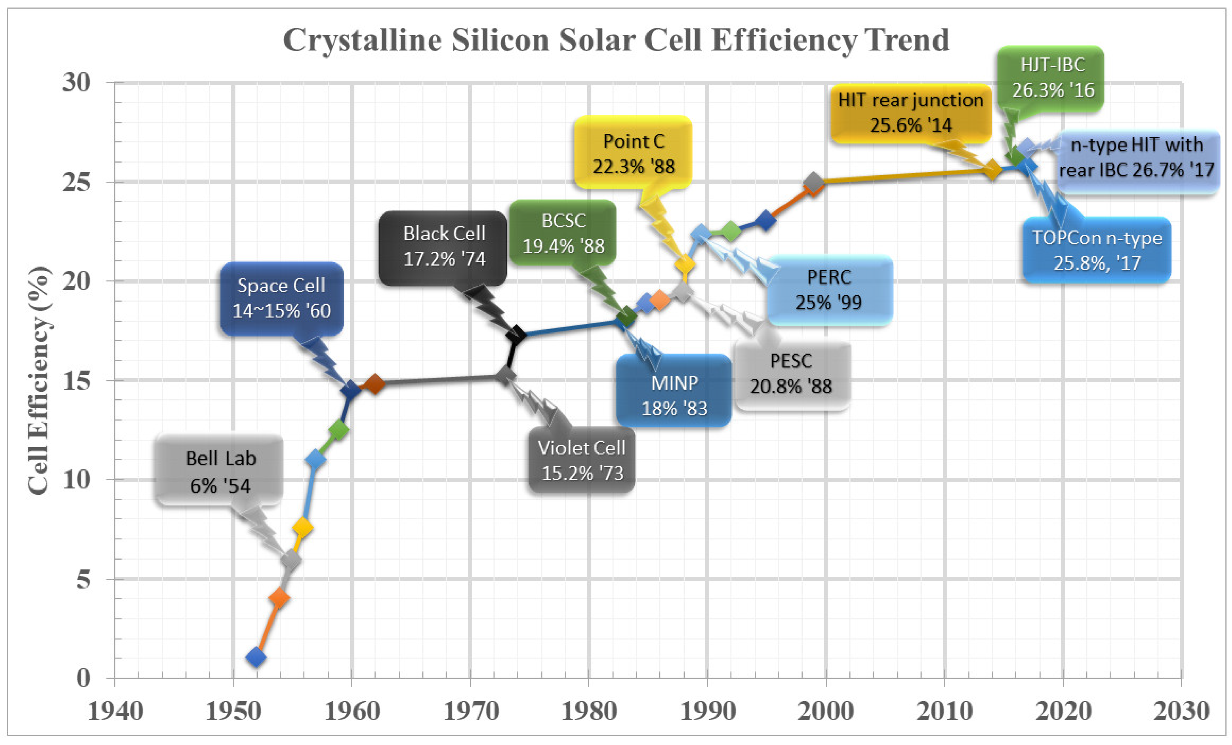
2. Development Progress of TOPCon Solar Cells

The efficiency of conventional industrial solar cells increased by 0.5 to 0.6% annually and is approximately 22% along with the structure of passivated emitter rear cells (PERC) during recent years [17,18,19]. While the efficiency of Si solar cells has reached 23%, the majority of the loss of recombination in these solar cells is caused by metal contact. Consequently, contact passivation has been a research concern of solar cells owing to various lapses. Numerous sources and structures were investigated, but this manufacturing concern extends to TOPCon as well [20]. In the TOPCon cell, the metal does not come into direct contact, a substitute, a nano-scaled tunneling oxide is deposited with a highly doped layer of n-poly or p-polysilicon that contacts the end metal. The function of the device is not influenced by the tunneling oxide as the tunneling oxide prevents a single form of carrier. Consequently, such arrangements of the cell structure are frequently described as passivating contacts. In 2010, interdigitated back contact (IBC) cells were fabricated by the SunPower Corporation by utilizing the passivating contacts [21]. Fraunhofer ISE fabricates TOPCon cells with 25.8% efficiency, [22,23] and POLO-IBC (poly-Si on oxide-interdigitated back-contacted) solar cells with 26.1% efficiency [24] were identified as having a 4 cm2 surface area. Motivated by such outstanding study developments, attempting to establish passive contacts in industrial-scale solar cell fabrication is intriguing. Nevertheless, there are several manufacturing conditions to be concerned about. At present, a large silicon wafer having dimensions of 156.75 × 156.75 mm2, 161.7 × 161.7 mm2, 166 × 166 mm2, 182 × 182 mm2, 210 × 210 mm2, or more is utilized. Moreover, a polysilicon deposition system is required for a high-efficiency solar cell because the roles of polysilicon are contact, in-diffusion barrier action, field-effect, gettering, and light absorption. However, there are approximately four distinct methods for commercial-scale fabrication: low-pressure chemical vapor deposition (LPCVD), ref. [25] plasma-enhanced CVD (PECVD), ref. [26] inline atmospheric pressure CVD (APCVD), ref. [27] and sputtering system [28]. Assessment of continuous utilization of such deposition methods for the photovoltaic industry is currently in its early development stage. Thin polysilicon film metallization is the third substantial requirement, and the process employed in the industry is high-temperature screen printing. At high temperatures, after the destruction of the firing-through paste, the task is to ensure the nano-scaled deposition of the tunnel oxide/poly-Si layer. Firing with Ag paste eliminates the nano-scale polysilicon layer that transforms Ag nanoparticles into c-Si and additionally improves the saturation current density J0 at the passivating contact section [29]. The metal contact saturation current density was studied at approximately 35 fA/cm2 [30]. The layer of polysilicon with a thickness of more than 150 nm can endure firing at high temperatures, and alternatively, these layers of polysilicon have a larger absorption coefficient [31] and originate absorption losses. The improvement of suitable metal pastes is currently disputed in the manufacturing of photovoltaic cells in the industry. Irrespective of the current challenges, by analysis of the “Levelized cost of electricity” (LCOE), TOPCon solar cells having n-type configuration are strong contenders for the majority next to the efficiency of PERC cells to increase up to 23% [32,33]. Recent research launched a newly constructed TOPCon cell; a maximum efficiency of 24.58%, and 716.8 mV Voc was recorded. Such components are presently produced at a large scale by many companies [34].
With the application of advanced technologies, traditional solar cells having the formation of p-type polycrystalline silicon were substituted by the cells of aluminum back surface field (Al-BSF) along with passivated emitter rear contact (PERC) solar cells [8,35]. The formation of PERC cell minimizes the losses caused by electrical and optical parameters with the combined layer of dielectric passivation on the backside. The selection of the material for the Al2O3/SiNx layer of passivation, wherein Al2O3 is deposited next to the SiNx layer, can improve by SiNx metallization [36].
Of late, PERC solar cells have been receiving a lot of attention owing to their minimum recombination losses and ability to hold the enhanced and improved efficiency in conjunction with Voc. Such a type of solar cells can be feasible because of the deposition o the insulating layer at the backside after constricted deletion to endure the metal contact of the absorber. LONGI solar accomplished the best efficiency of 24.02%, and the polycrystalline solar cell by Jinko achieved 22.04% efficiency with the technology of PERC solar cell [37,38]. The improvement in the technology of PERC solar cell is primarily concentrated on the construction of the emitter, replacement with multiwire interconnection from rectangular bus bars system, management of extensive lifetime of the cells, etc. The international directive of PV evaluations estimated that the technology of PERC solar cells has fast progress of greater than 60% more than the past decades. The design of PERC solar cells deteriorates by light-induced degradation (LID) and potential-induced degradation (PID), which considerably influence the working of the solar cell [39,40]. The heterojunction (HJ), heterojunction back contact (HBC), heterojunction with an intrinsic thin layer (HIT), and interdigitated back contact (IBC) solar cells are some of the supplementary technologies in the solar cell industry accompanied by PERC solar cells that have noticeable progress in solar cell efficiencies. The development of similar technologies in the years from 2010 to date and the forecast for future evaluation are shown in Figure 3 [14]. It can be envisaged from the graph that the technologies of TOPCon and HBC solar cells have great future potential because they are highly efficient and industrialized extremely fast. A total of 24% efficiency was achieved by SunPower in 2010; in 2016, the maximum solar cell efficiency was approximately 25.3%, utilizing the IBC solar cells [41,42].
The technological design of IBC along with HIT solar cells had a recent maximum efficiency of 26.7% [43,44] because of which HIT technology has moved to industrial production from laboratory research in recent years. On a commercial scale, the production cost of HIT solar modules is extremely expensive in comparison with PERC solar modules owing to exclusive substantial resources; for example, the silver paste of minimum working temperature and less consistency by the necessary industrial development of PV modules.
The recent structures of solar cell were recommended by a nano-scale silicon oxide passivating layer as well as carrier contact incapacitated by poly-Si. Using the advantage of HIT solar cell surface passivation and defeating the commercial inconsistency efforts by a recognized indoctrinated PERC manufacturing system, a preliminary attempt was made with the existing method in bi-polar junctional transistors in the 1970s [45]. A thin layer of SiOx was effectively combined by incapacitating the poly-Si to construct the structure with passivating contact. Such kinds of solar cells including poly-Si or oxide contact are known as polysilicon on oxide (POLO) or Tunnel Oxide Passivated Contact (TOPCon) solar cells [46,47].
TOPCon solar cells have experienced an immense rise in their manufacturing technologies and efficiency since 2010, as indicated in Figure 3 [48]. Comprising the IBC contact, 25.8% efficiency was accomplished, which is relatively greater than that of the HIT (25.2%) solar cell. The development in the efficiencies of TOPCon solar cells explains the exceptional grade solar cells that can be fabricated in extremely marginal manufacturing phases. Carrier transport appears because of the nano-scale layer of tunnel oxide by quantum tunneling, and by managing the surface recombination maximum open-circuit voltage Voc can be achieved [49]. The most recent study achieved 26% solar cell efficiency with a rear junction solar cell design which means the “emitter” is close to the rear surface instead of close to the front surface. In comparison with traditionally fabricated commercial bifacial solar cells, in which the rear side of the cell has metal grids rather than a full area covered with metals, the light reflected from the ground/roof (albedo) can enter the rear side and be absorbed by the solar cells again and increase the power output [50].
The foremost and necessary factors limiting c-Si solar cells are the recombination loss in metal contact and current-transport pathways in two or three dimensions. At the c-Si or oxide interface, by providing chemical passivation, the minimum defect density (Dit) that behaves as an impediment for the scattered doped material to c-Si from the poly-Si is utilized, although consequently the transport of charge carrier by the c-Si to the poly-Si is permitted. Along with reducing the further conduction of another charge carrier, it can be decreased by incapacitating the poly-Si that has outstanding conduction for individual charge carriers [46,49]. The conventional layout of the TOPCon solar cell is presented in Figure 2. The fabrication phases are comprehensible and reliable at the elevated temperature for diffusion. Appearing in the layout of the solar cell, the complete section of the rear part is contained in the passivated tunnel oxide metal contact and affects the one-dimensional transportation of current [51].
The production facilitates significant mitigation in the recombination of metal contact. It predominantly reduces the progress of interrupting connections, and the charge density consequently decreases [52,53]. The best quality deposit characteristic of tunnel oxide with a particular depth is required for effective passivation by chemicals, which then allows carrier transportation using tunneling, as expressed in the c-Si/SiOx/poly-Si energy band graph (Figure 4) [51,54]. Consequently, the probability of possible obstruction in preference to holes is more than electrons. The electrons tunnel all the way through the SiO2 layer; however, the holes are avoided. Collecting the solar cell photo-generated current from a tunnel oxide involves maintaining the thickness as fine as feasible which is useful for the transportation of current.

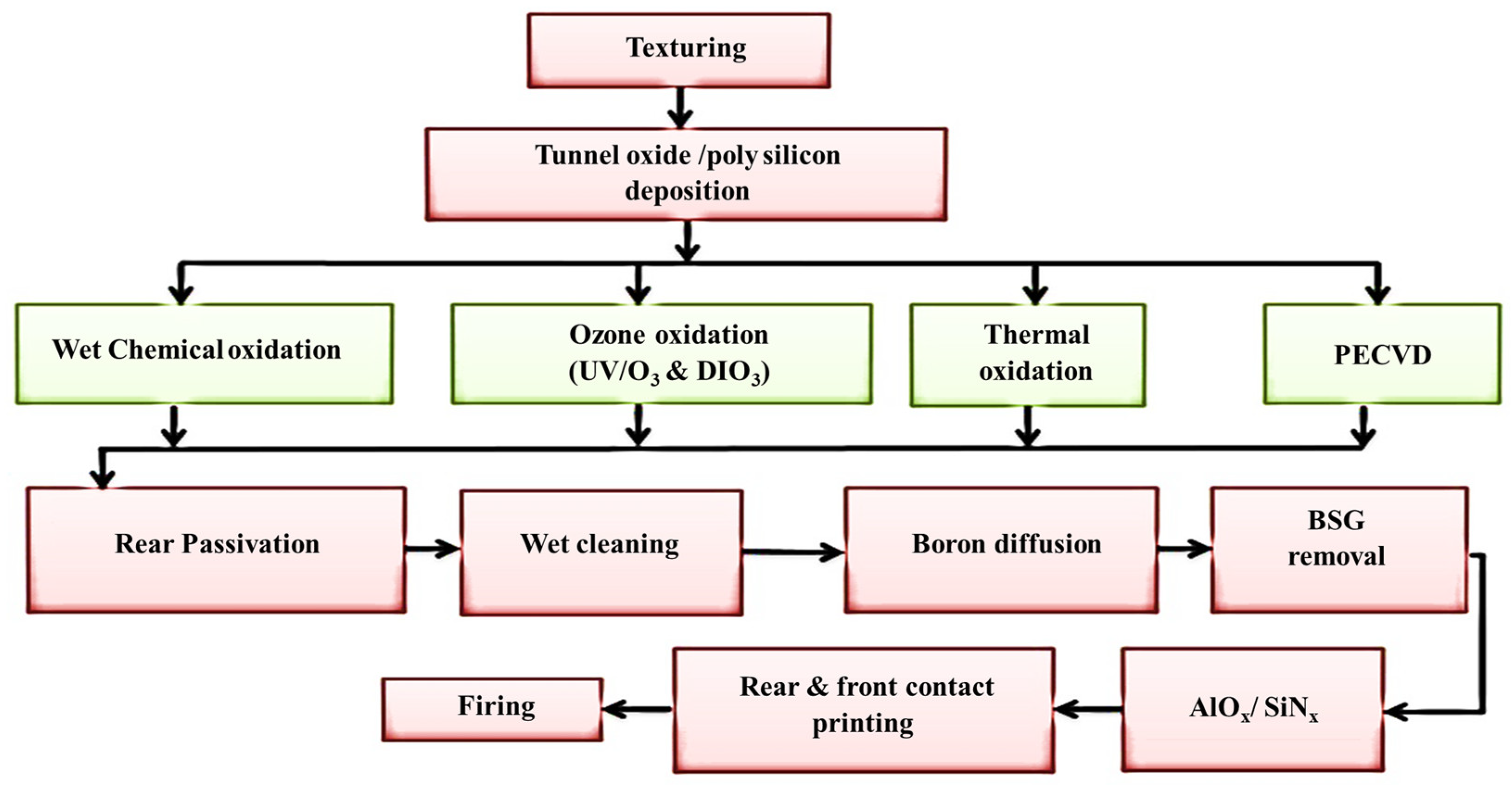
2.1. TOPCon Solar Cells Fabrication

The manufacture and construction layout of the cell is shown in Figure 5. It is fabricated on the front side with a boron emitter and backside with a passivating connecting layer, as well as with equal side fingers applied through a screen-printed approach to build a bi-facial solar cell. Small quantities of oxygen are needed for doping the wafers by phosphorus, including a resistivity value of about 0.4 Ω cm to 1.1 Ω cm. By utilizing a potassium hydroxide (KOH) solution, the wafers are textured on both sides with the pyramids of the irregular pattern. Following the RCA cleaning process and applying the boron tribromide (BBr3) gas, the boron emitter is produced in the furnace of boron diffusion. The backside boron diffusion is removed by applying the etching process on one side by utilizing the solution of nitric acid and hydrofluoric acid (HF/HNO3). The thermal oxidation is performed before the Boron Silicate Glass (BSG) removal. A tunneling SiOx layer is thermally established when wafers are cleaned with chemicals. For the PECVD, silane (SiH4), hydrogen (H2), and phosphine (PH3) are used as precursor gas sources for phosphorus-doped amorphous silicon (n-a-Si:H) growth. After annealing at 900 °C in a N2 environment for the dwell time of 30 min, n-a-Si:H is transformed into phosphorus-doped poly-Si layers (n+-poly-Si), which comprised n+-poly-Si on the c-Si/SiOx structure (n+-poly-Si/SiOx/c-Si contact). The boron emitter that passivated through the layer of the dielectric film, consequently, further RCA cleaning is carried out, specifically similar work out as anti-reflection layer of coating. The backside SiOx/n+-polysilicon coating is enclosed with PECVD SiNx:H. On both surfaces, an “H-metal contact” with Ag busbars is applied through screen printing for metallization. Subsequently, a quick-firing method with a maximum temperature of approximately 760 °C is applied [33]. Following the fabrication of the TOPCon solar cell, further essential solar cell characterizations such as IV curves and further considerations remain premeditated with a relevant 1-sun (1000 W/m2) IV analyzer.

2.2. Background of TOPCon Solar Cell Development Progress

In the past few years, the c-Si solar cell has been meticulously studied. When the metal is completely contiguous with the silicon wafer, the consequence is extreme electrical loss owing to the presence of electrons recombination in the solar cell because of the higher absorption of electrons at the junction area. In the preceding model, around two methods remained to decrease the metal carrier recombination accurately within the interaction with the silicon wafer: (1) through retaining a minor layer of the passivated silicon film, and (2) by diminishing the interaction capability and with the help of effortlessly developed doping to separate the metal from silicon wafer [56,57,58].
The main advantage of the foregoing methodologies is a passivated emitter and rear cell (PERC), that is after a conventional PN junction construction, with indigenous doping only in the contact area of the emitter. Currently, its efficiency at the current condition can achieve maximum of 25.0% [59]. The next approach for the previous method is heterojunction with intrinsic thin-layer (HIT) solar cells, as described by the Panasonic company. Such solar cells currently depict an efficiency of these cells around 26.7% [59,60].
The TOPCon solar cell can moreover seem as consequential after the typical PN junction structure, associated with the improvements of the two techniques described before. During the past few decades, owing to commendable passivation, the TOPCon solar cell turned out to build for the majority of research across technical organizations. The solar cell having n-type wafer with complete specific selective back contact charge carrier and double-sided interconnected solar cell, including a maximum efficiency, was reported to have approximately 26.7% efficiency by Fraunhofer [59,60]. The maximum efficiency is owing to the fact wherein the n-type wafer provides a superior impurity that permitted improvement, and the flaws in the faces are passivated entirely. The majority of the materials being revealed that substrate resistivity between 1 and 10 Ω cm utilized for the TOPCon solar cell are able to achieve an efficiency higher than 25% [58]. For the improvement in the efficiency of solar cells and to retain a process that should be capable of continue to enhance, the selective contact charge carrier comes to developed in the proposed TOPCon solar cell. Unlike conventional silicon type of solar cells, TOPCon achieves the following important characteristics and key features [61,62]:
  • The ultimate oxides layer at the nano-scale assured the hanging bond that is found at a single crystal surface, consequently improving the conversion efficiency;
  • Depending on the range of substrate conductivity, the oxide layer at nano-scale level permits instant transport of the holes or electrons;
  • Owing to the importance of the high possibility of densely doped polysilicon conductivity, the junction resistivity can be reduced, and the output current might become better.

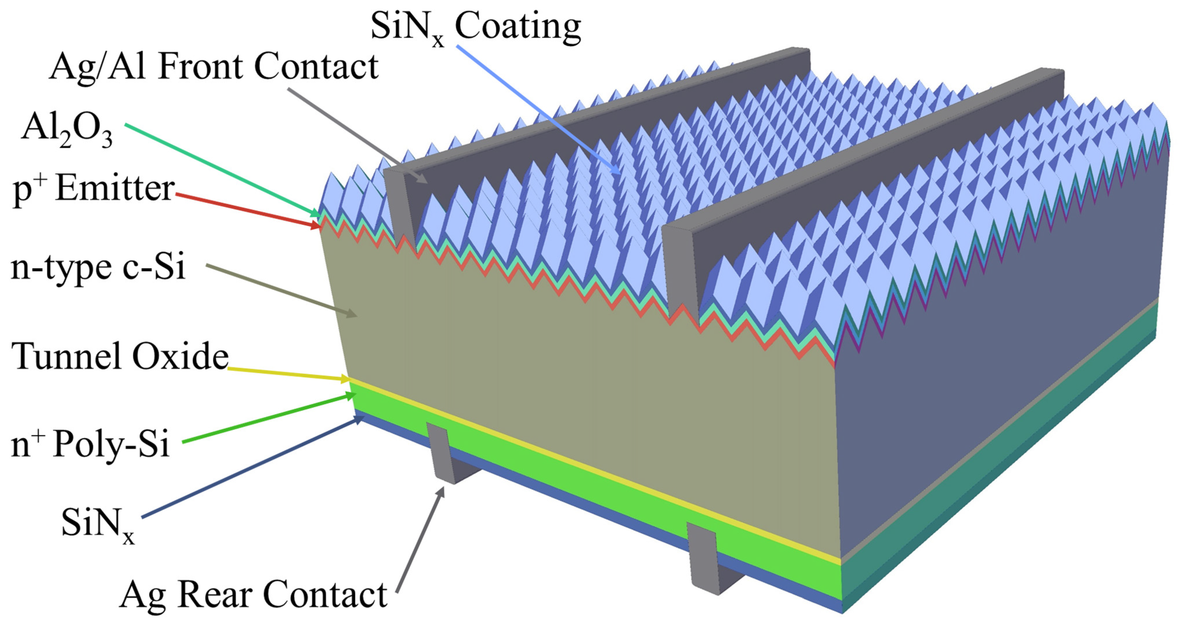
2.3. Structure of TOPCon Solar Cell

The elementary design of the TOPCon solar cell structure is shown in Figure 2, mainly generated with a PN junction on the substrate of an n-type material [58,63]. The cell is passivated with a nano-scale layer of aluminum oxide (Al2O3) on the p-type material surface and includes an extremely thin coating of approximately 2 nm with a Silicon dioxide (SiO2) tunneling layer and a highly doped polysilicon layer on the n-type material surface [64]. The surface passivation by the tunneling oxide layer is the most important attribute of the TOPCon solar cell, along with the selective contact to accomplish the exceptionally minimum recombination level after the highly doped layer of polysilicon. To permit many of the carriers to the tunnel, the tunneling layer of SiO2 requires to be sufficiently fine to transport though. Similarly, their field effect must be able to prevent transmission of the minority carriers [65]. Properties of the passivation layer for the highly doped level of the polysilicon layer are varied by adjusting the concentration rate of hydrogen through physical vapor deposition (PVD). For instance, atomic layer deposition (ALD) sputtering, or chemical vapor deposition (CVD) such as plasma-enhanced chemical vapor deposition (PECVD), or low-pressure chemical vapor deposition (LPCVD). Because of the enormous amount of hydrogen atoms in the highly doped polysilicon layer, it shows reasonable properties of passivation [66].

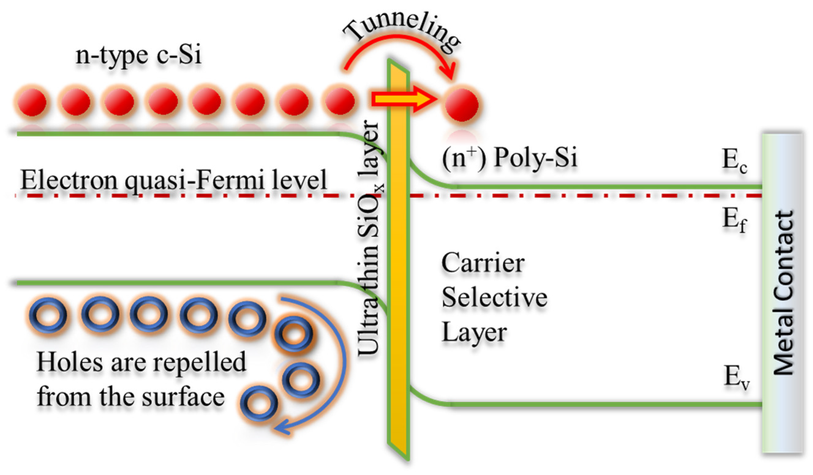
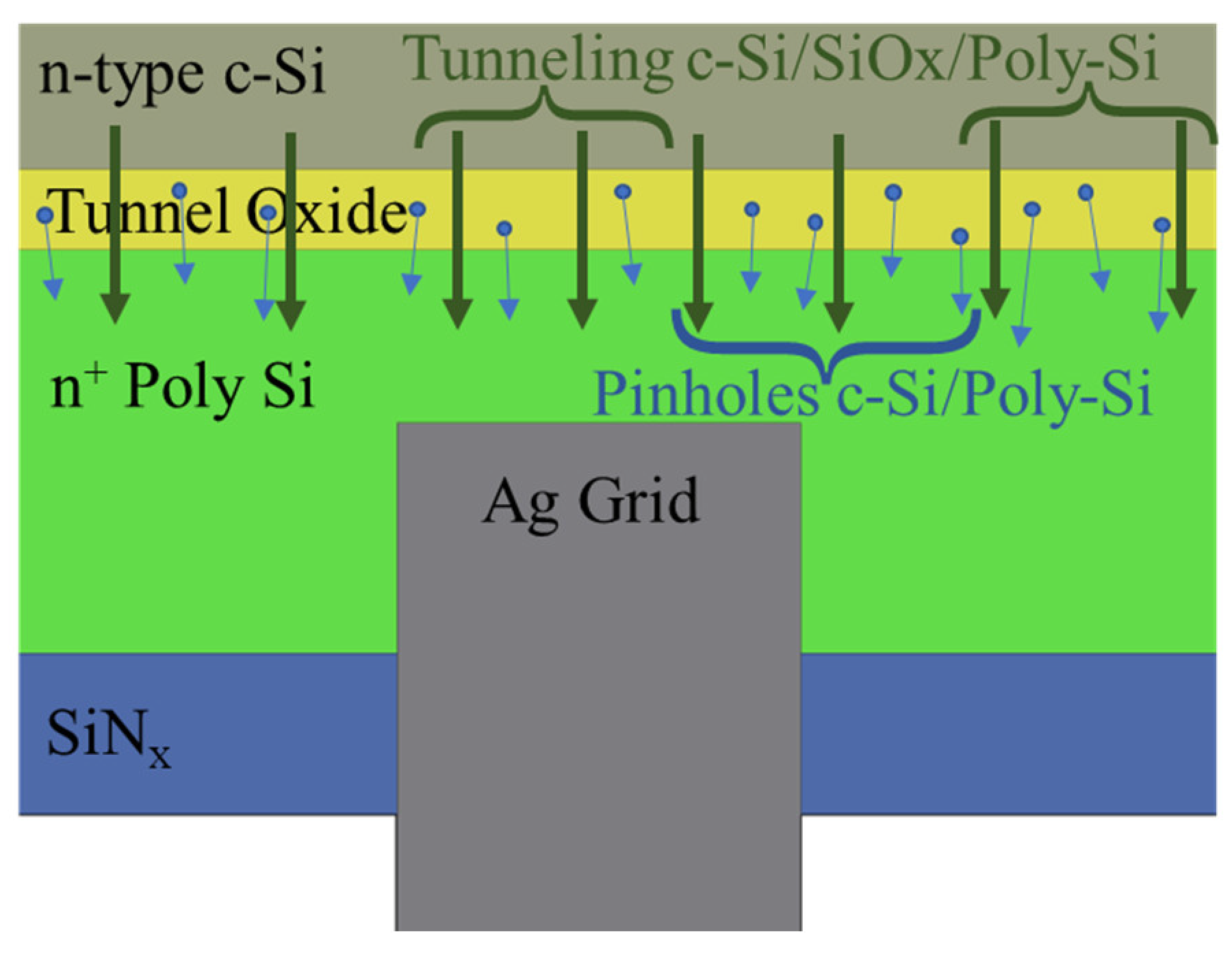
2.4. Carrier Transportation Mechanisms at the Poly-Si/SiOx/c-Si Interfaces in the TOPCon Structure

The trends of pinhole and tunneling are two unique forms of charge carrier transportation configurations that arise at interfaces of poly-Si/SiOx/c-Si. Figure 6 demonstrates the situation of carrier transport that happens at the layer of SiOx. Such structures take place according to the width of SiOx thickness and annealing temperatures.
Feldmann et al. explored SiOx tunneling layer experiences maintaining thicknesses of not more than 1.5 nm [52]. The main charge carrier conduction was investigated through the tunneling layer by SiOx. Recent research was enhanced by the simulation modeling performed by Steinkemper et al. The energy band chart in Figure 4 illustrates selective charge carriers that tunnel across the layer of nano-scaled SiOx in the structure of TOPCon solar cell [14,48,55].
Likewise, the process of the pinhole occurs with a thickness of more than 2 nm of SiOx that is significantly annealed at higher temperatures of approximately 1000 to 1050 °C. The resulting prevalent technique for such kinds of contacts remained precisely controlled over pinholes within the c-Si layer along with poly-Si which were developed through annealing at a high temperature in the SiOx layer [67,68]. Although the oxide layer thickness is conflicting in different progress methods [46], the trend of tunneling takes place in oxides from not more than 2 nm because it is incredibly challenging to tunnel the charge carriers by concentrated oxide coatings [69]. The findings after the performance simulation by Zhang et al. upon nano-scaled tunnel oxide (SiOx, less than 1.5 nm) layer show very high features of tunneling and efficiency by preventing the carrier transport by pinhole [70]. However, a relatively dense SiOx layer (more than 1.1 nm) exhibited minimum fill factor (FF), and efficiency through larger resistivity does not permit any carrier transportation beyond the pinholes.
The transportation of the minimum carrier over the pinholes improves the FF and minimizes the resistance, consequently enhancing the PCE. Wietler et al. analyzed restrain carrier transport by pinholes through selective etching surface of oxide layer on the junction of the POLO structure [53]. A greater density of pinhole concentration would generate maximum saturation current density and negligible contact resistivity (ρc) of approximately 10 mΩ cm2. The thickness of the SiOx layer entails the electrical characteristics of the TOPCon solar cell. The current investigation by Wang et al. described three distinct oxide layer thicknesses as 1.25, 1.42, and 1.55 nm, which exhibited inconsistency in efficiency and other electrical parameters of TOPCon solar cells [71]. At 1.55 nm oxide layer thickness, good quality and regular surface are obtained after the etching, and it holds a minimum J0 value of approximately 18 fA/cm2, with FF = 81.09% and Voc = 687 mV. However, the nano-scaled oxide layer at the thickness of 1.25 and 1.42 nm shows insufficiencies that are ascribed to the passivation failure at the nano-scaled oxide layer along with the pinhole’s progression. Adjusting the accurate temperature for annealing, this one decreases the development of pinhole concentration [72]. The exceptional productivity preceding technology of the TOPCon solar cell continues to determine the specific thickness of the nano-scaled tunnel oxide layer and efficient pinhole concentration for the enhancement in efficiency. The TOPCon solar cell structure holds the lowest value of saturation current density (J0) for equally p-type and n-type poly-Si around (J0 = 2 to 8 fA/cm2). Previously, the doping of poly-Si through phosphorous had better qualities than the poly-Si with boron-doping [73]. However, through research, it became obvious that the n-TOPCon has a good property for the layer of passivation between c-Si wafers of p-type and n-type, demonstrating an excellent value of Voc in comparison with the p-TOPCon [41].
It is not only tunneling that moves the charge through the pinholes; both the transportation through the pinholes and the tunneling occurs together. For example, excessively thick oxide might provide a high tunneling barrier, although charge transfer through pinholes is possible. However, tunneling is more prevalent in the case of dense nano-scaled oxide. The type of conductivity is the factor that matters most. Due to the band-bending orientation, it was shown that p-Si/SiOx/p+-Si can only transport holes and not electrons, and vice versa.

3. Development of Nano-Scaled Oxide Layer on TOPCon Solar Cell

Effective procedures for the development of TOPCon solar cell nano-scaled oxide layers with thicknesses around 1.3 to 1.5 nm include thermal oxidation, wet chemical dipping, and ultraviolet ozone cleaning (UV/O3) treatment. In addition to the intelligible techniques to generate the nano-scaled oxide layer is wet chemical dipping in an acidic combination solution at a temperature greater than 90 °C. The development of thermal oxidation is able to remain separated also within dry and wet oxidation with oxygen, consistent with the consumption of oxidizing atmosphere. Clean as well as dehydrated oxygen is utilized instead of dry oxidation as oxygen gas such as oxidizing environment to produce an oxide layer on elevated temperatures; oxygen responds immediately to hydrazine gas. For an oxidizing atmosphere, wet oxygen is an ultimate fine vapor of clean water, utilized to fabricate the oxide layer with water molecules and the reactive oxide surface. Normally, the oxidation rate with dry oxygen is less than that of wet oxygen oxidation [61,64].

Polysilicon Doped Layer

The heavily doped polysilicon layer is fabricated by (1) employing LPCVD by accumulation on the part of the silicon, reconcilement in addition to doping with extra ions, or (2) utilizing PECVD and accurately relegating the doping level to a silicon layer.

4. Techniques for Deposition of Tunnel Oxide Layer on TOPCon Solar Cells

The flowchart depicted in Figure 7 shows the conventional measures that were examined for the fabrication of the TOPCon solar cell. The layer of tunnel oxide can be established through the use of various oxidation methods such as ozone oxidation, chemical oxidation, thermal oxidation, and plasma-enhanced chemical vapor deposition (PECVD) oxidation.
In addition to other sources such as Al2O3, SiNx, or a-SiNx, silicon oxide (SiOx) is also very widely accessible and can be used as a material for tunnel coating and as layers for passivation in the TOPCon solar cell [74,75]. Regarding progress that is related to the efficiency of the TOPCon solar cell and can be improved by maintaining the thickness of the tunnel oxide layer to be under 2 nm. The progress of subsequent nano-scaled SiOx is extremely complicated because it triggers several difficulties during deposition alongside the carrier transport phenomenon. Recent techniques concisely reflect different oxidation methods that are identified in advance of SiOx depositing together with the layer of tunnel oxide and the impact of the accumulation requirements on solar cell characterizations appearing in every process.

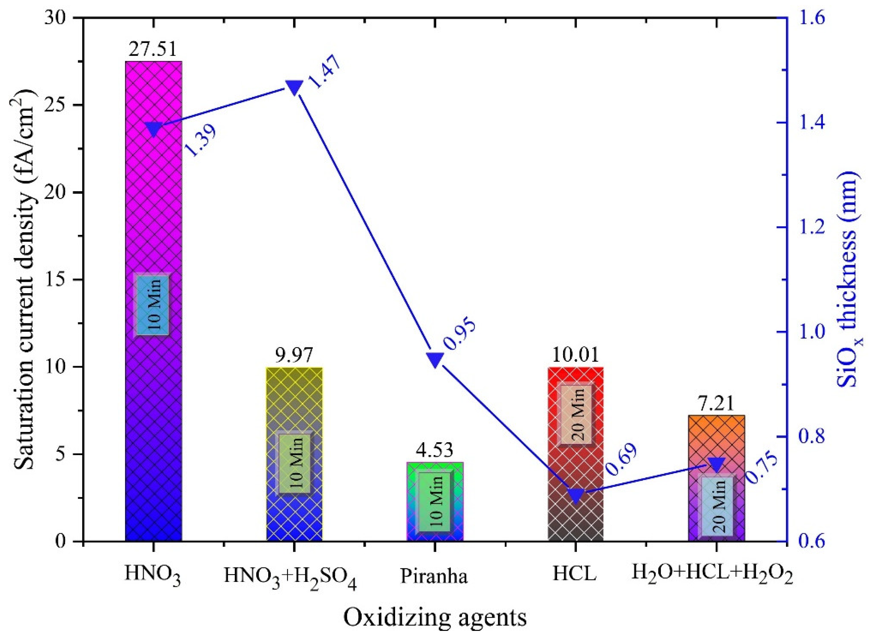
4.1. Chemical Oxidation

Wet chemical oxidation in Si is accomplished for the development of SiOx as a tunnel oxide layer through the use of several acidic atmospheres such as hydrochloric acid (HCl), sulfuric acid (H2SO4), nitric acid (HNO3), a combination of acids, and amalgamation of acids through the hydrogen peroxide (H2O2) such as the solution of piranha [76,77]. Along with several additional acidic chemicals, HNO3 is an established technique used during chemical oxidation for the creation of the SiOx layer in the development of various microdevices and is known to improve the Si/SiO2 interaction characteristics. The oxidation of Si with nitric acid showed the direct connection-level absorption and continuous interaction of Si/SiO2 layers accompanied by the different additional chemical oxidation (e.g.,: H2SO4:H2O2, HCl:H2O2,) nearly at 120 °C environments [78]. The oxidation reaction takes place at the lowest temperature because of the HNO3 disintegration as shown in Equation (1) below; very strong atomic oxygen along with effective oxidizing energy was developed. The distribution of atomic oxygen through the improvement of the SiO2 layer reacts with the Si/SiO2 interface.
2HNO3 → 2NO + H2O + 3O
Matsumoto et al. discovered that 68 wt% HNO3 holds the lowest leakage current and caused the atomic density to increase by approximately 7% compared with the 61 wt% HNO3 that thermally generated SiO2 [78]. In conjunction with HNO3, a SiO2 layer with a thickness in the range of 0.7 to 1.5 nm can be created and probably observed by changing the temperature. Temperature is a very crucial element in the chemical mixture that enhances the possibility of oxidation. Raising the temperature by more than 90 °C is not ordinary to the technologically present techniques of wet chemicals because HNO3 evaporates and transforms through the acid composition. Those techniques point to the intricacy associated with the creation of an oxide layer with good reliability and exceptional quality but low imitation. Another method reported by Tong et al. revealed a decent level of tunnel silicon oxide (SiOx) across a mixture of one volume of H2SO4 (98 wt%), and three volumes of HNO3 (68 wt%) were recognized as condensed nitric and sulfuric acid (CNS) [77].
The CNS-grown SiOx layer plays an exceptional role along with the advanced condition of oxidation by 60 °C that decreases the acid evaporation and persists extraordinary throughout the time of the growing method. The typical rise in implied open-circuit voltage (iVoc) with 2.5 to 10 mV and average individual surface dark saturation current density (J0) fall from 1 to 7 fA/cm2 in comparison with pure HNO3 that fabricate the SiOx tunnel oxide layer. The SiOx layer established using the CNS acid on the solar cell has the ability to raise the efficiency by approximately 0.15%.
The depth and the successive diffusion J0 for the SiOx tunnel oxide layer that can be accrued through the utilization of various acids are depicted in Figure 8. The combination of HNO3:H2SO4 in the 3:1 ratio requires a specific thickness of approximately 1.3 to 1.5 nm of the SiOx layer at 60 °C including a contact time of 10 min. Using the solution of piranha and reaching oxidation led to the formation of the SiOx layer at approximately 1 nm with an incredibly low saturation current density of J0 = 5 fA/cm2 in conjunction with additional chemical oxidation. The chemical oxidation approach can be employed at the manufacturing scale and is therefore associated with temperature control. It can be used in the manufacture of the efficient solar cell. However, the pinholes that are built at the surface of the oxide layer with 1000 °C annealing temperatures help in improving J0 and further impact damage to the oxide layer [79]. Comparably, nano-scaled SiOx layers ranging from 1.3 to 1.5 nm established across the chemical oxidation show minimum chemical oxides and are vulnerable to being disrupted at high annealing temperatures [80].

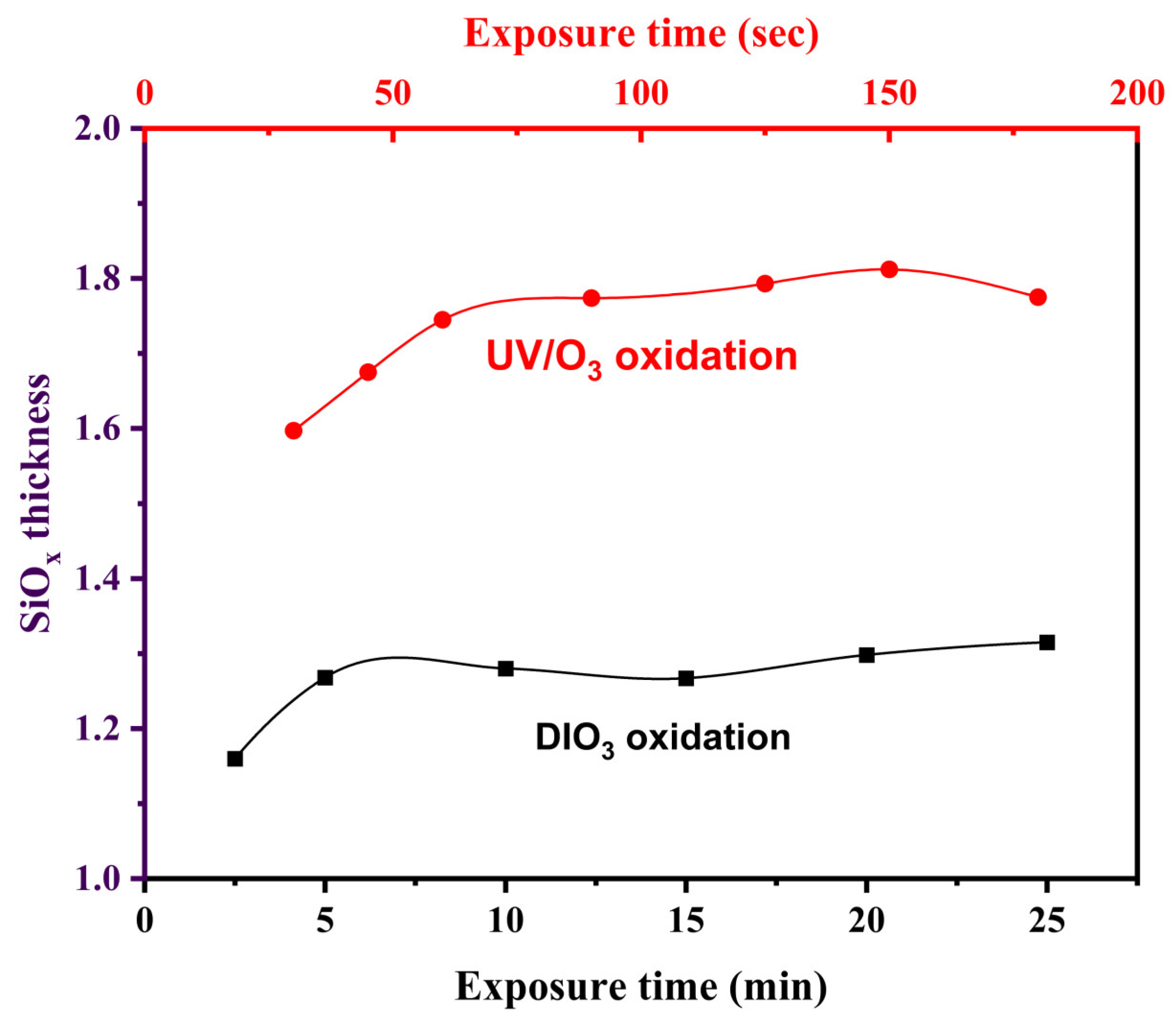
4.2. UV and DI Ozone Oxidation

Ozone (O3) is extremely ambiently responsive to oxidizing chemicals such as HNO3, NO2, and N2O, that decay into molecular oxygen at the lowest possible temperature [81]. The oxidation of silicon through ozone can be achieved similarly via de-ionized ozone oxidation DIO3 (wet) and in a photo-oxidation UV/O3 (dry) environment. The oxygen produced in this manner has high density and low kinetic energy and leads to the creation of an assessment model that is highly secure even after high-energy particles attack it. The photo-oxidation of O2 requires the use of photons with energy greater than 7.2 eV in order to enhance the inadequacy of progress on the interaction layer [82]. Chao et al. studied ozone for silicon oxidation in its initial phase and reported that the minimum intensity of ozone increases the level of oxidation within an environment of oxygen [83]. A structure of tests showed that the Si/SiO2 interrelating plane generated by O3 is additionally receptive and improved compared with the external interface established using conventional O2. It reduces the intersecting level of transformation and requires less effort [84,85]. In the literature, several types of ozone manufacturers are available for silicon oxidation [86]. In this regard, a UV-assisted ozone creator can continually deliver appropriate ozone molecules. UV-light exhilarated ozone crystallizes Si in parts and the product thus obtained improves properties of the oxide at room temperature, similar to the multi-c-Si. The diffusive oxygen radical mixture functions perfectly in the dispersion of suspended bond links and generates minimum inadequacy in terms of intensity compared with the O2-produced oxygen [87]. For this reason, Si ozone oxidation serves as an intriguing area of investigation. In the past few years, different ozone oxidation techniques were applied for the production of a nano-scaled SiOx oxide layer in the TOPCon solar cell sample. Moldovana et al. examined the mutually refining process of oxidation using UV/O3 and employed a Hg vapor bulb with a wavelength of λ = 185 or 254 nm and an excimer component with a wavelength of λ = 172 nm on a textured and smooth surface at the same time for transparent silicon [88]. The refined tunnel oxides of UV/O3 suggested that the iVoc of approximately 720 mV for the plane surface and 710 mV on the textured specimen subsequent annealing at 900 °C is comparatively improved through assessment by the progress of the HNO3 oxide. The layout within the cell sample and time of exposure showed a substantial impact on iVoc and the highest exposure time of approximately 3 min was found to be adequate for the well passivating layer of the SiOx with a thickness ranging from 1.6 to 1.8 nm, as indicated in Figure 9.
SiOx can also be developed using ozone via wet chemical ozonation (DIO3). For over ten years, the manufacture of semiconductors has been explored through the application of ozone scattered into powerful de-ionized water (DIO3); this ensures that the semiconductors are better protected and that the wafers are clean. A similar technique reduces the number of components employed in the production method for the manufacture of solar cells and consequently reduces the extent of acquisition [89]. The most current research by Vossen et al. demonstrated that wet compounds oxidized in ozone water can be used for the efficient generation of the tunnel oxide layer with a thickness of 1.1 to 1.5 nm within 30 min, as demonstrated in Figure 9 [90]. Subsequently, at 850 °C annealing temperature, the oxide can be established for passivation and oxidation can be reduced by increasing the temperature to compensate for the deficiency in the passivated layer. The saturation current density of DIO3 in the dark condition produced oxide has a minimum extent because it is related to the dried O3 oxidation.
Scientists have compared the TOPCon solar cell characteristics obtained via the deposition layer of the SiOx tunnel oxide using three distinct methods of oxidation [91]. The efficiency of all the three types in proximity to various temperatures for annealing, for example, were based on ozone oxidation Tanneal = 900 °C for the (UV/O3 and DIO3) and HNO3 chemical oxidation Tanneal = 800 °C. The method of DIO3 oxidation indicated further stability of the oxide and along with the three methods, the passivation was enhanced.

4.3. Thermal Oxidation

At the silicon layer, thermal oxidation permits two types of oxidations. One has a moderate temperature and an elevated pressure of oxygen gas, and the other is vice versa. The oxide development effect occurs according to Equation (2), even though there is no effective model for the mechanism of oxidation used for such procedures in the instance of nano-scale layers [92]. At elevated temperature, response and minimal pressure of oxygen gas accompany Equation (3) which disintegrates the Si/SiO2 and vice versa.
Si + O2 → SiO2
Si + SiO2 → 2SiO
The kinetics of oxidation of Si are described adequately in this section. The characteristics of passivation for the preparation of SiO2/Si with thermal interaction, particularly the impact of the dimensions, structure, and fundamental conversion were comprehensively examined [93]. Increasing the temperature for annealing those effects on the oxide layer showed no development of pinholes in the produced nano-scale oxide layer thermally with less than 1.5 nm thickness until 850 °C; nevertheless, tunneling is the prevailing procedure in this regard [94]. For impenetrable oxide layers with a thickness greater than 2 nm, raising the temperature for annealing causes a reduction in the dark saturation current J0 below 1000 °C, and an additional increase in temperature upsurges the value of J0 because of the increase in the pinhole density, in addition to a decline in the contact resistivity [53]. The temperature ranging from 550 to 650 °C develops an oxide layer with a thickness of 1.6 nm demonstrating persistent oxide coating followed by 850 °C annealing along through carrier transport process due to tunneling [71]. The thickness versus saturation current density of thermally developed layers of SiOx under various temperatures is shown in Figure 10. As can be seen, the layers of nano-scale SiOx, which were 1.5 nm each and annealed at elevated temperatures demonstrated an extreme saturation current density (J0). This can be a result of the deterioration of oxide reliability at high temperatures of annealing for nano-scaled layers of SiOx. The minimum possible saturation current density was examined for different layers of SiOx with thickness greater than 2 nm and annealed at extremely elevated temperatures. Such coatings annealed at elevated high temperatures are highly endurable. The various layers of SiOx with thicknesses ranging from 1.2 to 1.5 nm produced using different chemical, thermal, DIO3, and UV/O3 oxidation methods, as well as thermally developed layers, revealed better passivation at 1000 °C with regard to annealing. The thermally developed oxidation layer was the most appropriate as it decreased the density at the interface and shows less J0 carrier selective contact for the p-type on the annealing temperature of 950 °C and for p-type silicon with the highest minority carrier lifetime [90,94].
Another approach for developing the SiOx coating for enhanced efficiency of the cell as well as carrier lifetime is rapid thermal oxidation (RTO). Liu et al. developed the SiO2 layer via RTO and demonstrated a 19.49 μs carrier lifetime with a nominal 0.87% reflectance [95]. An additional model developed by Liao et al. produced the coating of SiOx with the RTO thermal oxidation method in two stages [96]. The developed layer indicated enhanced efficiency of the cell, minimum surface recombination velocity, and improved carrier lifetime, which is approximately 15.45 μs.

4.4. Plasma Enhanced Chemical Vapor Deposition (PECVD)

Within traditional solar cells, the nano-scaled layer development utilizing the thermal oxide involves a temperature scale ranging from approximately 850 to 1050 °C and improves the thermal cost and consequently the total expense. A basic economical and minimum temperature manufacturing technique must be established for confronting financial disputes. Plasma-enhanced chemical vapor deposition (PECVD) is an efficient method for passivation at the minimum cell temperature, and the substratum temperature varies from 250 to 350 °C [96,97,98]. The PECVD technique was applied for the development of a layer with SiOx for both n-type and p-type solar cells along with the assistance of CO2 gas, temperature, and pressure. The method of oxidation in the PECVD process can be performed using various treatments of plasma oxygen: RF, DC discharge, or microwave. In oxygen plasma, the simplest approach to developing the nano-scale oxide layer is the direct oxidation of Si. Antonenko et al. evaluated the development design and layer characteristics within the plasma-producing medium along with inert and oxygen gas mixtures (O2: Ar, O2; He, O2) [99]. It was noticed that the Si endured intense oxidation in plasma generated by immaculate helium gas. Further research was conducted by a team that discovered the development of silicon oxide kinetics at the exterior side of Si through oxygen plasma management [100]. The temperature of the substrate ranging from 20 to 200 °C, levels of doping, and type of conductivity have a marginal effect on the development of the SiOx layer.
Mandal et al. described a SiOx layer with a thickness of approximately 1.8 nm using the PECVD oxidation method at 250 °C temperature by utilizing 13 MHz RF plasma in an atmosphere of CO2 gas along with 1 torr pressure and 60 mW/cm2 power density [101]. Within such a procedure, the highest impediment peak of 0.287 eV was attained for Si wafer having an n-type configuration along with a textured surface. Huang et al. established a plasma endorsed nitrous-oxide (N2O) gas oxidation method for the deposition at nano-scaled silicon oxide (SiOx), considering the temperature of the substrate, time of treatment, and control of the plasma power [102]. The N2O plasma oxidized SiOx indicated individually restrained thickness with different acidic oxidation [80,99]. The highest implicit voltage (iVoc) of 730 mV and 4.3 fA/m2 recombination saturation current (J0) was attained for individual portions. In additional research by Tian et al., a nano-scaled layer of SiOx was developed on a p-type c-Si wafer by plasma-aided N2O [103]. The researchers examined a better feature of passivation at an improved temperature of annealing than for the layer of SiOx produced by acidic oxidation. The technique decreased the cost of production by incorporating the manufacturing of SiOx and amorphous silicon in a particular compartment, utilizing the in-line PECVD oxidation method.

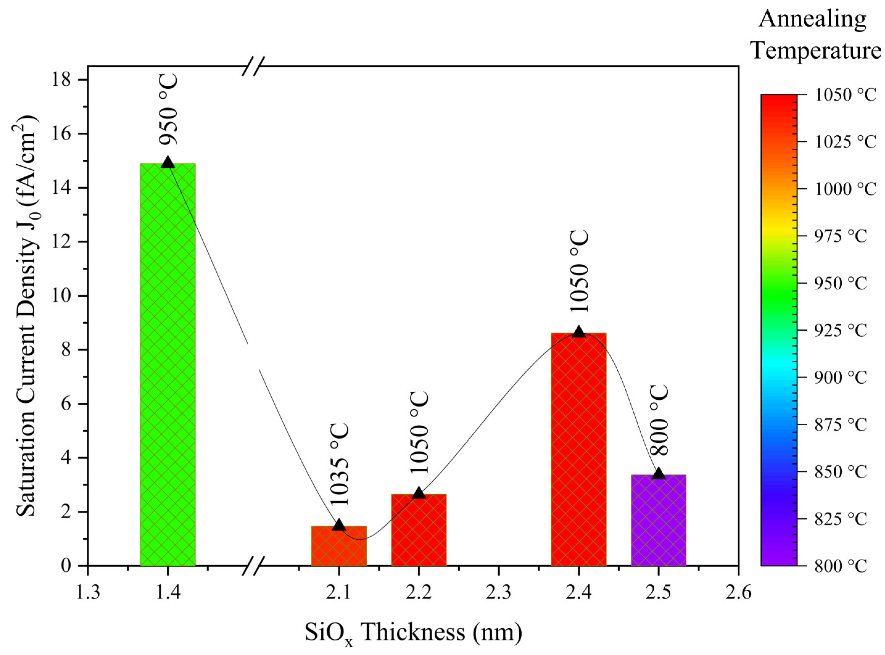
5. Analysis of Loss Factor

The characterized loss factors are classified according to four groups: bulk limit, optical, recombination, and resistance loss. The bulk limit is verified as 32.92%, with a consequent 5.32% loss because of bulk J0 at 10 fA/cm2 and a decrease in efficiency to 27.60% on point ①, as demonstrated in Figure 11 and Figure 12. Next is the optical loss that is affected because of the shading at 0.65%, reflection at the front side by 0.38%, and loss from escape by 0.02%, which decrease the efficiency up to 26.95%, 26.57%, and 26.55%, indicated at points ②, ③, and ④, respectively, as shown in Figure 11 and Figure 12. Recombination loss is the third loss factor that is triggered by the front passivation by 0.37%, front contact at 0.40%, and rear passivation contact of 0.11%, which additionally reduce the efficiencies to 26.18%, 25.78%, and 25.66% as expressed at points ⑤, ⑥, and ⑦, respectively, as demonstrated in Figure 11 and Figure 12. The final loss factor is attributable to the resistance of the electrical circuit which is resistance owing to a shunt of 0.10% and series of 0.46%, which affect and cause a reduction in efficiency to 25.56% and 25.10%, as disclosed at points ⑧ and ⑨, respectively, in Figure 11 and Figure 12. The loss factor assessment of efficiency is explained in Table 1 by the current density (mA/cm2), open-circuit voltage Voc (V), fill factor FF (%), efficiency loss (%), and the ultimate efficiency.

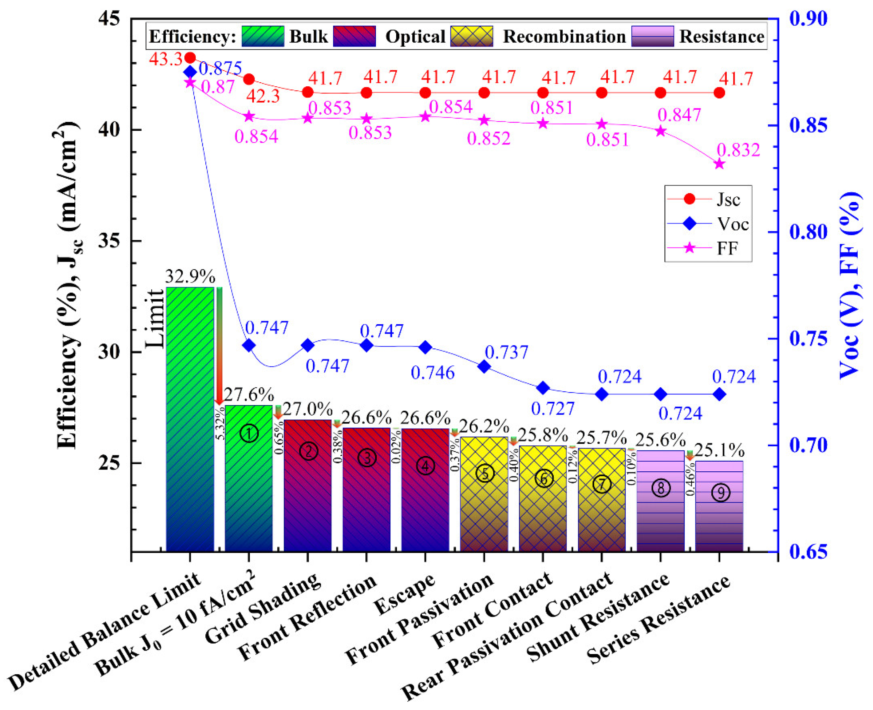
5.1. n-Type TOPCon Solar Cell TCAD Analysis and Conversion Efficiency with Bifaciality

From the rear-side contact, the n-type TOPCon solar cell bifaciality and conversion efficiency were evaluated by optimization of finger width. The TCAD assessment was performed by adjusting the finger width from the backside, ranging from 1200 to 25 μm, and on the front and backside, the output efficiency was examined by analyzing the bifaciality by dividing up the backside to foreside efficiencies.
The efficiency at 25 μm width at the rear finger was reported to be 23.01% from the fore face and 20.83% for the back surface. At this width, the bifaciality appeared to be 90.53%. As the back surface finger width increased, the efficiency of the back surface of the cell fell considerably, although the fore surface efficiency of the cell improved marginally. With the 1200 μm finger width at the back surface, the efficiency of the back surface of the cell fell to 7.33%. The efficiency at the fore cell surface rose to 23.74%, and the bifaciality was determined to be 1.74% because of the minimal back surface efficiency of the cell. The back surface efficiency was lowered by raising the width of the finger at the back surface, and the efficiency at the fore surface was improved while the finger width at the back surface was enlarged. Therefore, the maximized efficiency value could be determined using the back surface width of the finger at F1 + R0.2. This implies adding up 100% value of efficiency at the fore surface and the 20% value of efficiency from the back surface efficiencies. The optimal finger width thickness at the back surface side was 100 μm because the back surface efficiency was 19.85%, and the fore surface efficiency was 23.35%. As demonstrated in Figure 13, by compiling efficiencies of both sides, the optimal efficacy obtained was 27.37% with the F1 + R0.2 combination [104]. The rear finger resistance loss can be marginally decreased with increased rear finger width due to a greater cross-sectional area, which results in a modest gain in cell efficiency as measured from the front side. If we move beyond the optimal point, the efficiency would be lowered by combining the front and rear efficiencies. We achieved an ideal result of about 100 µm rear metal width thickness through this simulation. Changing the optimized rear metal width has a negative influence on efficiency due to recombination current density (J0). If we deviate more or less from the optimized (100 µm) metal width value, a compromise in efficiency is seen as shown in Figure 13. According to Table 2, the tunnel oxide layer’s optical thickness is 1.5 nm. We used this thickness for the bifaciality simulation in order to maximize the TOPCon solar cell’s overall performance.

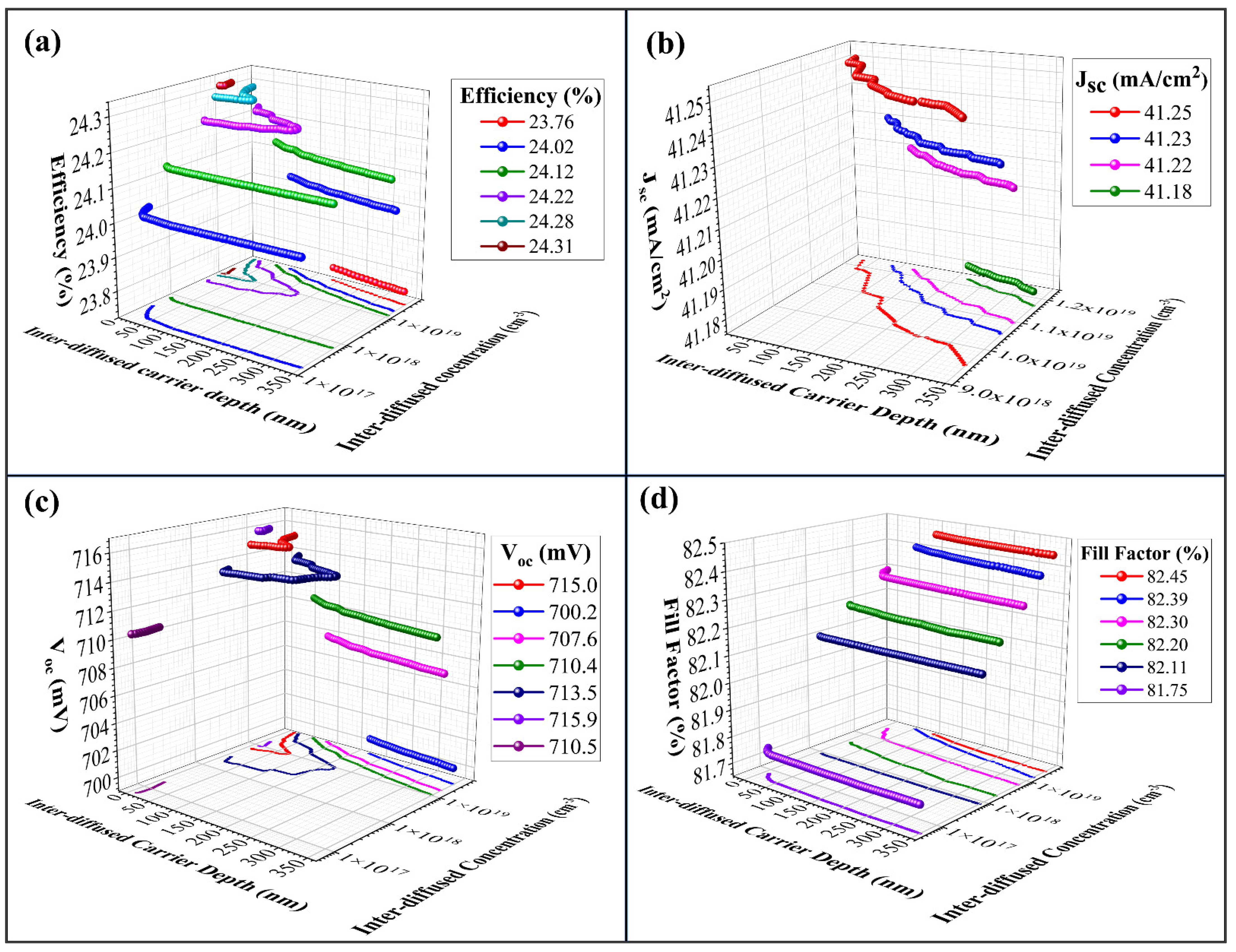
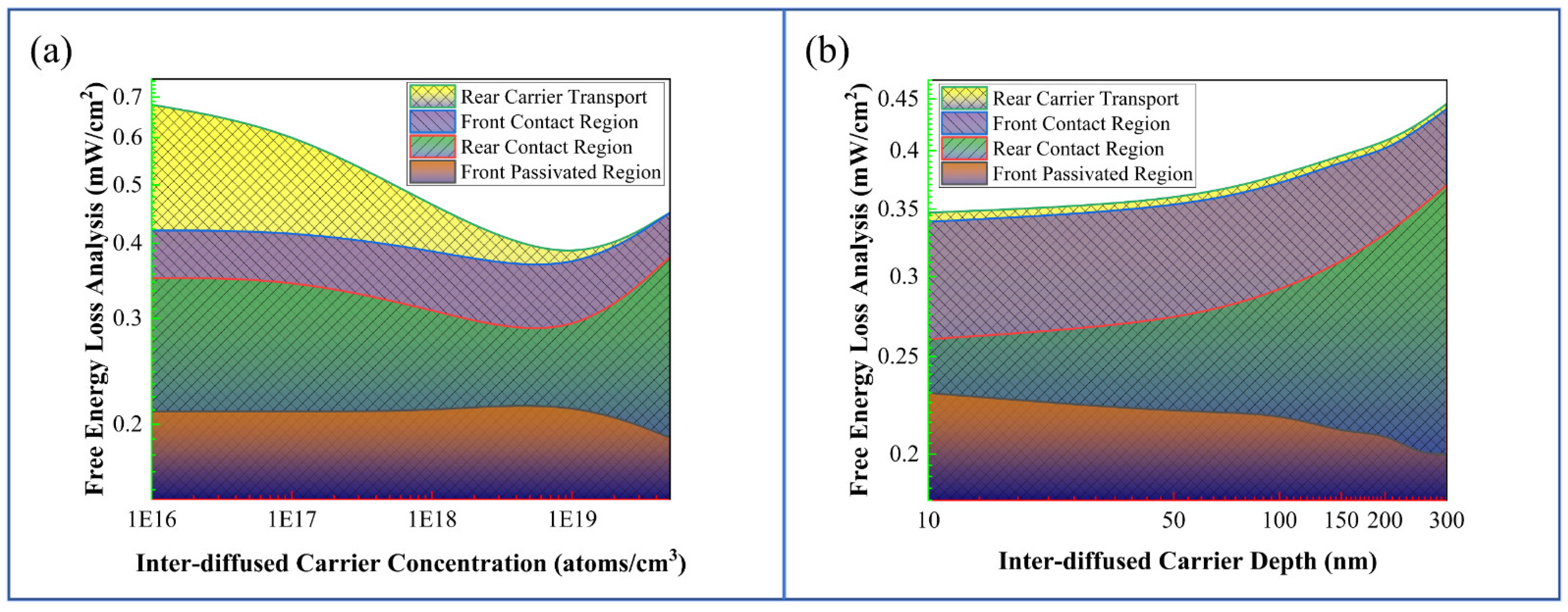
5.2. Investigation of Interfuse Concentration

Base/substrate and emitter are the two primary sections of a conventional Si solar cell. The inter-diffusion dopant concentration distribution in the emitter area has a significant impact on the performance of Si solar cells; a good emitter always ensures greater performance. For a specific emitter diffusion profile, the peak concentration (i.e., the dopant concentration at the substrate surface) and the depth factor (i.e., the depth below the surface at which the dopant concentration is reduced to 1/e of the peak concentration) determine the total inter diffusion dopant concentration at any given point inside the emitter region. As a result, optimizing the emitter diffusion profile is a crucial prerequisite for a highly efficient Si solar cell. The inter-diffusion can be defined as p- or n-type, and in any instance, the profile of the diffusion can be uniform, exponential, Gaussian, or Erfc. Understanding the microstructural changes in silicon solar cells at any temperature requires comprehension of inter-diffusion processes and diffusivity of impurity atoms, which may be supported by phase equilibrium investigations. A three-dimensional (3D) contour chart is prepared based on the inter-diffused carrier depth (nm) and inter-diffused concentration (cm−3) for several factors: efficiency (%), current density (mA/cm2), open-circuit voltage Voc (mV), and fill factor (FF) (%); as demonstrated in Figure 14 the characteristics of carrier selective contact solar cells were studied by simulation in accordance with the inter-diffusion concentration and depth of impurity. The impurity of inter-diffusion changes with temperature and time and is dependent on the solubility of each impurity. A structure was created by assuming the properties of the n+ layer in silicon since the phosphorus impurity was employed for the Electron Selective Contact (ESC) layer in this simulation. The concentration was modified from 1 × 10¹⁶ atoms/cm3 to 5 × 10¹⁹ atoms/cm3 and the depth from 10 to 350 nm for inter-diffusion of impurity to the back substrate in the TCAD Tool. The inter-diffusion concentration and depth of impurity values acquired from this simulation data were included in the TCAD analysis. Their solubility, which changes with temperature and time, determines the inter-diffusion of impurities. Although phosphorus was employed as an impurity in the ESC layer, a simulation framework was developed by assuming the properties of the silicon n+ layer. In the TCAD tool, the depth was modified from 10 to 350 nm, and the impurity concentration was increased from 1 × 10¹⁶ atoms/cm3 to 5 × 10¹⁹ atoms/cm3. The inter-diffused layer impurity concentration increased from 1 × 10¹⁶ atoms/cm3 to 1 × 10¹⁹ atoms/cm3, which resulted in higher conversion efficiencies as shown in Figure 14a. However, as Figure 14b illustrates, there is no major fluctuation in the current density. As seen in Figure 14c,d, the open-circuit voltage and fill factor fluctuate in relation to changes in impurity concentration. While the FF declines, the Voc rises when the inter-diffused carrier depth is lowered. For the higher inter-diffused carrier concentration at the shallowest depth, a high-efficiency result was attained. As instance, the fill factor displays the greatest fill factor of 82.4% for the concentration of 5 × 10¹⁹ atoms/cm3 with an etching depth of 100 nm; nevertheless, the open-circuit voltage dramatically decreases (below 710 mV, as shown in Figure 14c) due to the rise in Auger recombination. The difference in the electric field and resistance with regard to the inter-diffused impurity on the back side is what causes this change in the cell parameter. For a deeper investigation of the solar cell characteristics with regard to the variation in each parameter, as shown in Figure 15, free energy loss analysis (FELA) was performed. The variation in loss as a function of inter-diffused impurity concentration is seen in Figure 15a. The impurity concentration of 1 × 10¹⁹ atoms/cm3 resulted in the lowest loss of 0.36 mW/cm2, which is consistent with the conversion efficiency trend. When the concentration reaches 5 × 10¹⁹ atoms/cm3, Auger recombination becomes dominant, which causes a rise in the loss due to the rear contact. The change in cell efficiency with regard to inter-diffusion depth is seen in Figure 15b, as the depth rises, the loss increases as well. When the inter-diffused depth is increased from 10 to 350 nm, the rear contact loss increases from 0.03 mW/cm2 to 0.17 mW/cm2, respectively. Reduced conversion efficiency results from this rise in rear contact loss with the inter-diffusion carrier depth [104].

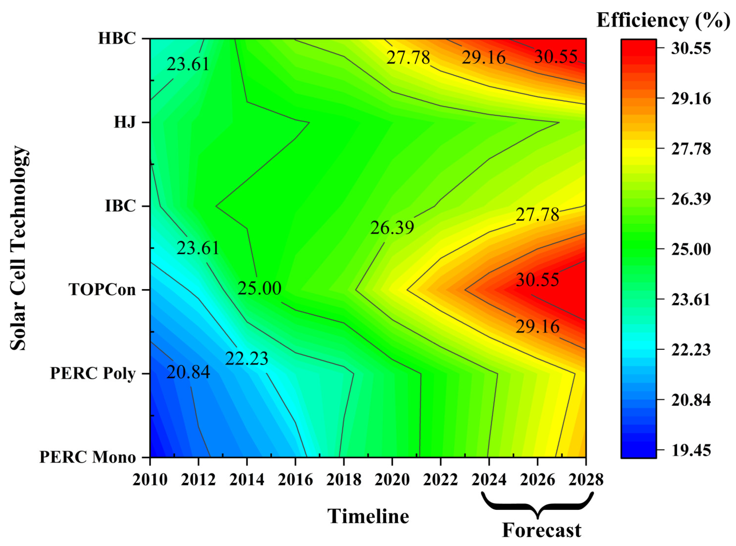
6. Perspective for the Future Research and Overview

After PERC solar cells, TOPCon solar cells are the leading innovative cells at an industrial scale, and they can comprehend the current advanced technology production process as PERC along with the additional nano-scale coating of tunnel oxide of approximately 1 to 3 nm. The favorable findings achieved explicate that TOPCon is an impending and higher productivity solar cell. In the current stage of the TOPCon cell production process, SiOx is the most frequently applied layer for tunnel oxide. Various methods of deposition have been employed to produce the layer of tunnel oxide. The methods being used increasingly for oxidation to accumulate the nano-scale layer of SiOx within TOPCon solar cells comprise chemical, ozone, thermal, and PECVD oxidation, which were concisely reviewed. The different approach has a distinct influence on merits and demerits in the progress of the essential nano-scale layer of SiOx, which relies on the investigational requirements. For instance, a nano-scale layer of SiOx can be developed by utilizing H2SO4:HNO3 chemical oxidation at the lowest possible temperature of approximately 60 °C. Ozone oxidation has the benefit of staying naturally benevolent, and it can further develop thermally balanced layers of SiOx. The technique of thermal oxidation can develop the layer of tunnel oxide and has velocity at an ultra-low surface recombination level of approximately 10 cm/s. PECVD oxidation can develop the layer of SiOx on several substrates within a limited time, and thus it might be an economical approach.
Certain illustrations of every method of oxidation and a comparison of the specifications of each cell are presented in Table 2. After literature review, it can be inferred that the constraints of the cell for instance charge carriers’ conduction through the layer of SiOx is not established on the development of tunnel oxide coating thickness. Currently, there are two kinds of passivated layers of tunnel oxide in accordance with the development of SiOx layers of various thicknesses. One is greater than 2 nm, and the other is less than 1.6 nm in thickness.
The predominant performance of conduction for the previous category is pinhole and tunneling for the subsequent. Some additional crucial factors which affect the thickness of the SiOx layer are the temperature of annealing, time, and the method of oxidation utilized for the development. Among the methods of oxidation, chemical, ozone (UV and DI), thermal, and PECVD, the thermal and PECVD methods produced deposits of SiOx and revealed outstanding passivation, owing to which such layers are impenetrable and have incredibly limited bulk deficiencies.
Alternatively, research was conducted to find a replacement for SiOx as a layer of tunnel oxide. For instance, Al2O3 was examined as a layer of tunnel oxide favorable for the manufacturing of the TOPCon solar cell. The latest research by Lu et al. demonstrated the condition of passivation for equally n-type and p-type TOPCon solar cells by SiOx, AlOx, and AlOx/SiOx as dual layers of tunnel oxide [108]. They discovered that the SiOx exhibited improved passivation in comparison with the additional two layers of tunnel oxide. The dopant diffusion improved by utilizing the AlOx for boron in p-type TOPCon and overcame the phosphorous in the diffusion of n-type TOPCon solar cell. Such an influence turns out to be just as conspicuous with AlOx/SiOx dual layer. A comparable performance has been examined in some additional articles [109,110]. Correspondingly, Wen et al., utilized SiNx as a layer of tunnel nitride rather than a SiOx layer of tunnel oxide [75]. They accumulated a layer having a thickness of 2.5 nm SiNx as a tunnel using the method of catalytic chemical vapor deposition. It has a 0.8 ms lifetime at an elevated temperature of annealing, and the contact resistance was assessed to be 0.014 Ω cm2. Although there is some information studying the feasible replacement and variations for the layer of tunnel oxide in TOPCon solar cells, strong investigation and improvement are extremely necessary for this area, which is deprived of negotiating the efficiency of the cell and its parametric factors. There are few new results on the conversion of the layer SiO2 passivation to enhance the implementation on the solar cells containing particular deficiencies, polymer layer deposition, and accumulation of dopants to produce heterogeneous structures [111,112,113,114,115]. This might be an additional interesting area of investigation to enhance the implementation of TOPCon solar cells.
Thus far, manufacturers have been attempting to commercialize the TOPCon cell; however, there are limitations in industrializing TOPCon cells, such as the process of metallization, consumption of silver being twice that of other cells, being discovered typically on wafers of n-type material, and containing one or two further progressions in comparison with PERC solar cell. In the future, further investigation is necessary to improve the economical TOPCon solar cells with the current efficiency. Obtaining a substitute for the layer of SiOx tunnel oxide and industrializing the TOPCon solar cells devoid of negotiating the efficiency is currently an important issue of investigation.

7. Conclusions

In the TOPCon solar cells’ progress, it was conducive to employ a series of continuous analyses and explicated research for achieving an independently incurable consecutive efficiency of 24.58%. The indicated efficiency is on a bigger wafer containing busbars and fingers with metal, extensive illumination, and fabricated with manufacturing production instruments. The evaluation validates that emitter recombination losses, including its bulk, surface, and metal contacts are preventive of the execution of the device, even though the passivating contact of the rear side has a minimum J0 of less than 7 fA/cm2, by the 94% non-metalized part with J0 = 3.4 fA/cm2 and 6% metallization portion through J0 = 50.7 fA/cm2. It is achieved by improving the emitter and its metallization but assumes a good capability for additional efficiency enhancements. This can be completed by further development of a conventional formation method of the emitter and its paste metallization or by replacing it with a transparent passivating contact. In this study, curtailing the polysilicon passivating contacts performance and developing a deliberate passivating contact that is precisely feasible were of utmost importance for silicon photovoltaic research and development. The industry of solar photovoltaics is dominated by c-Si solar cells nowadays. Although interdigitated back contact cells reveal the highest efficiency, bifacial solar cells are less complex and are the recommended option for commercial manufacturing. Excellent optoelectrical qualities for both-sides-contacted cells lead to a conversion efficiency of 26.0% by eliminating the layers at the front side that allow lateral charge carrier transport using TOPCon technology. Diverse conventional industrialized solar cells that construct a PN-junction at the front and back of these solar cells or have a PN-junction in the form of a complete surface passivation contact with polysilicon. A comprehensive assessment of power loss indicated that such solar cells stabilize the electrons and hole transport losses, along with standard recombination and transport losses. Methodical simulation research has recognized certain essential layout guidelines for potential silicon solar cells with efficiencies of more than 26%, explaining the possibility and dominance of these back contact solar cells. Numerous methods are in use all over the world to fabricate the tunnel oxide layer for TOPCon solar cells. To deposit the thin layer of SiOx, TOPCon solar cells primarily use the PECVD oxidation, chemical oxidation, thermal oxidation, and ozone oxidation processes as described in this study. Each method has benefits and drawbacks depending on the experimental conditions for producing the required SiOx thin layer. In fact, a thin SiOx layer can be deposited using a straightforward wet process called chemical oxidation with HNO3:H2SO4 at temperatures as low as 60 °C. Similarly, ozone oxidation, which has the advantage of being environmentally friendly, can be used to grow more stable SiOx layers. The SiOx layer is also created by thermal oxidation, with surface recombination speeds as low as 10 cm/s. Growing SiOx layers on several substrates at once using PECVD SiOx deposition is an economical method.

Author Contributions

Conceptualization, H.Y., M.Q.K., M.A.Z. and J.Y.; methodology, H.Y., Y.K. and J.Y.; software, H.Y. and M.R.; validation, Y.K., D.P.P. and S.K.; formal analysis, M.Q.K., M.A.Z. and S.K.; investigation, M.Q.K., M.A.Z. and S.K.; resources, M.A.Z. and M.Q.K.; data curation, H.Y.; writing—original draft preparation, H.Y.; writing—review and editing, H.Y.; visualization, H.Y. and M.R.; supervision, Y.K. and J.Y.; project administration, Y.K. and J.Y.; funding acquisition, Y.K. and J.Y. All authors have read and agreed to the published version of the manuscript.

Funding

This research received no external funding.

Institutional Review Board Statement

Not applicable.

Informed Consent Statement

Not applicable.

Data Availability Statement

Not applicable.

Acknowledgments

This research was supported by grants from the New and Renewable Energy Technology Development Program of the Korea Institute of Energy Technology Evaluation and Planning (KETEP) funded by the Korean Ministry of Trade, Industry and Energy (MOTIE) (Project No. 20218520010100 and 20203040010320).

Conflicts of Interest

The authors declare no conflict of interest.

References

  1. Eriksen, R.; Engel, D.; Haugen, U.; Hodne, T.; Hovem, L.; Alvik, S.; Rinaldo, M. Energy Transition Outlook 2021: Technology Progress Report. 2021. Available online: https://www.dnv.com/Publications/energy-transition-outlook-2021-210847 (accessed on 14 March 2022).
  2. Aklin, M.; Bayer, P.; Harish, S.P.; Urpelainen, J. Does basic energy access generate socioeconomic benefits? A field experiment with off-grid solar power in India. Sci. Adv. 2017, 3, e1602153. [Google Scholar] [CrossRef] [PubMed] [Green Version]
  3. Lovins, A.B. A bright future: The rise of solar energy and the path ahead for America’s renewable energy sector. Science 2015, 350, 169. [Google Scholar] [CrossRef]
  4. International Energy Agency Photovoltaic Power Systems Programme (IEA PVPS). Snapshot of Global Photovoltaic Markets. 2020. Available online: https://iea-pvps.org/wp-content/uploads/2020/04/IEA_PVPS_Snapshot_2020.pdf (accessed on 14 March 2022).
  5. Chapin, D.M.; Fuller, C.S.; Pearson, G.L. A new silicon p-n junction photocell for converting solar radiation into electrical power. J. Appl. Phys. 1954, 25, 676–677. [Google Scholar] [CrossRef]
  6. Ghosh, D.K.; Bose, S.; Das, G.; Acharyya, S.; Nandi, A.; Mukhopadhyay, S.; Sengupta, A. Fundamentals, Present Status and Future Perspective of TOPCon Solar Cells: A Comprehensive Review. Surf. Interfaces 2022, 30, 101917. [Google Scholar] [CrossRef]
  7. Kim, S.; Kim, T.; Jeong, S.; Cha, Y.; Kim, H.; Park, S.; Ju, M.; Yi, J. Passivating Contact Properties based on SiOX/poly-Si Thin Film Deposition Process for High-efficiency TOPCon Solar Cells. New Renew. Energy 2022, 18, 29–34. [Google Scholar] [CrossRef]
  8. Green, M.A. The path to 25% silicon solar cell efficiency: History of silicon cell evolution. Prog. Photovolt. Res. Appl. 2009, 17, 183–189. [Google Scholar] [CrossRef]
  9. Yoshikawa, K.; Kawasaki, H.; Yoshida, W.; Irie, T.; Konishi, K.; Nakano, K.; Uto, T.; Adachi, D.; Kanematsu, M.; Uzu, H.; et al. Silicon heterojunction solar cell with interdigitated back contacts for a photoconversion efficiency over 26%. Nat. Energy 2017, 2, 17032. [Google Scholar] [CrossRef]
  10. Allen, T.G.; Bullock, J.; Yang, X.; Javey, A.; de Wolf, S. Passivating contacts for crystalline silicon solar cells. Nat. Energy 2019, 4, 914–928. [Google Scholar] [CrossRef]
  11. Yablonovitch, E.; Gmitter, T.; Swanson, R.M.; Kwark, Y.H. A 720 mV open circuit voltage SiOx: C-Si: SiOx double heterostructure solar cell. Appl. Phys. Lett. 1985, 47, 1211–1213. [Google Scholar] [CrossRef]
  12. Feldmann, F.; Bivour, M.; Reichel, C.; Hermle, M.; Glunz, S.W. A Passivated Rear Contact for High-Efficiency n-Type Silicon Solar Cells Enabling High Vocs and FF > 82%. In Proceedings of the 28th European PV Solar Energy Conference and Exhibition, Villepinte, France, 30 September 2013; pp. 988–992. [Google Scholar]
  13. Feldmann, F.; Steinhauser, B.; Arya, V.; Büchler, A.; Brand, A.A.; Kluska, S.; Glunz, S.W. Evaluation of TOPCon technology on large area solar cells. In Proceedings of the 33rd European Photovoltaic Solar Energy Conference and Exhibition, Amsterdam, The Netherlands, 25 September 2017; pp. 1–3. [Google Scholar]
  14. Liu, J.; Yao, Y.; Xiao, S.; Gu, X. Review of status developments of high-efficiency crystalline silicon solar cells. J. Phys. D Appl. Phys. 2018, 51, 123001. [Google Scholar] [CrossRef]
  15. Shaw, V. The Weekend Read: Life after PERC. Available online: https://www.pv-magazine.com/2021/05/08/the-weekend-read-life-after-perc/ (accessed on 14 March 2022).
  16. Lu, M.; Mikeska, K.R.; Ni, C.; Zhao, Y.; Chen, F.; Xie, X.; Zhang, C. Screen-Printable Conductor Metallizations for Industrial n-TOPCon Crystalline Silicon Solar Cells. In Proceedings of the 2021 IEEE 48th Photovoltaic Specialists Conference (PVSC), San Juan, Puerto Rico, 20–25 June 2021; pp. 954–957. [Google Scholar]
  17. Hermle, M. Silicon Solar Cells–Current Production and Future Concepts. Fraunhofer Institute for Solar Energy Systems ISE. 2017, pp. 1–46. Available online: https://www.helmholtz-berlin.de/media/media/projekte/hercules/hercules-m36-workshop/2016-10-10-hermle-berlin-bessy-pdf.pdf (accessed on 14 March 2022).
  18. Stenzel, F.; Lee, B.G.; Cieslak, J.; Schwabedissen, A.; Wissen, D.; Geißler, S.; Rudolph, T.; Faulwetter-Quandt, B.; Hönig, R.; Wasmer, S.; et al. Exceeding 23% and Mass Production of p-Cz Q. ANTUM Bifacial Solar Cells. In Proceedings of the 36th European Photovoltaic Solar Energy Conference and Exhibition, Marseille, France, 9 December 2019; pp. 96–99. [Google Scholar]
  19. Rahman, M.Z. Advances in surface passivation and emitter optimization techniques of c-Si solar cells. Renew. Sustain. Energy Rev. 2014, 30, 734–742. [Google Scholar] [CrossRef]
  20. Feldmann, F.; Bivour, M.; Reichel, C.; Hermle, M.; Glunz, S.W. Passivated rear contacts for high-efficiency n-type Si solar cells providing high interface passivation quality and excellent transport characteristics. Sol. Energy Mater. Sol. Cells 2014, 120, 270–274. [Google Scholar] [CrossRef]
  21. Cousins, P.J.; Smith, D.D.; Luan, H.C.; Manning, J.; Dennis, T.D.; Waldhauer, A.; Wilson, K.E.; Harley, G.; Mulligan, W.P. Generation 3: Improved performance at lower cost. In Proceedings of the 35th IEEE Photovoltaic Specialists Conference, Honolulu, HI, USA, 20–25 June 2010; pp. 275–278. [Google Scholar]
  22. Richter, A.; Benick, J.; Feldmann, F.; Fell, A.; Hermle, M.; Glunz, S.W. n-Type Si solar cells with passivating electron contact: Identifying sources for efficiency limitations by wafer thickness and resistivity variation. Sol. Energy Mater. Sol. Cells 2017, 173, 96–105. [Google Scholar] [CrossRef]
  23. Green, M.A.; Hishikawa, Y.; Dunlop, E.D.; Levi, D.H.; Hohl-Ebinger, J.; Ho-Baillie, A.W. Solar cell efficiency tables (version 51). Prog. Photovolt. 2018, 26, 3–12. [Google Scholar] [CrossRef] [Green Version]
  24. Haase, F.; Hollemann, C.; Schäfer, S.; Merkle, A.; Rienäcker, M.; Krügener, J.; Brendel, R.; Peibst, R. Laser contact openings for local poly-Si-metal contacts enabling 26.1%-efficient POLO-IBC solar cells. Sol. Energy Mater. Sol. Cells 2018, 186, 184–193. [Google Scholar] [CrossRef]
  25. Stodolny, M.K.; Lenes, M.; Wu, Y.; Janssen, G.J.M.; Romijn, I.G.; Luchies, J.R.M.; Geerligs, L.J. n-Type polysilicon passivating contact for industrial bifacial n-type solar cells. Sol. Energy Mater. Sol. Cells 2016, 158, 24–28. [Google Scholar] [CrossRef]
  26. Nandakumar, N.; Rodriguez, J.; Kluge, T.; Groβe, T.; Fondop, L.; Padhamnath, P.; Balaji, N.; König, M.; Duttagupta, S. Approaching 23% with large-area monoPoly cells using screen-printed and fired rear passivating contacts fabricated by inline PECVD. Prog. Photovolt. Res. Appl. 2019, 27, 107–112. [Google Scholar] [CrossRef]
  27. Merkle, A.; Seren, S.; Knauss, H.; Min, B.; Steffens, J.; Terheiden, B.; Brendel, R.; Peibst, R. Atmospheric Pressure Chemical Vapor Deposition of In-Situ Doped Amorphous Silicon Layers for Passivating Contacts. In Proceedings of the 35th European Photovoltaic Solar Energy Conference and Exhibition, Brussels, Belgium, 27 September 2018; pp. 785–791. [Google Scholar]
  28. Deng, S. Polysilicon Contacts for Next-Generation Industrial Silicon Solar Cells. UNSW. 2019. Available online: https://unsworks.unsw.edu.au/entities/publication/3218ed31-21bd-4acc-b5a8-499fd69847fd (accessed on 14 March 2022).
  29. Stodolny, M.K.; Anker, J.; Geerligs, B.L.; Janssen, G.J.; Van De Loo, B.W.; Melskens, J.; Santbergen, R.; Isabella, O.; Schmitz, J.; Lenes, M.; et al. Material properties of LPCVD processed n-type polysilicon passivating contacts and its application in PERPoly industrial bifacial solar cells. Energy Procedia 2017, 124, 635–642. [Google Scholar] [CrossRef]
  30. Padhamnath, P.; Wong, J.; Nagarajan, B.; Buatis, J.K.; Ortega, L.M.; Nandakumar, N.; Khanna, A.; Shanmugam, V.; Duttagupta, S. Metal contact recombination in monoPoly™ solar cells with screen-printed & fire-through contacts. Sol. Energy Mater. Sol. Cells 2019, 192, 109–116. [Google Scholar]
  31. Feldmann, F.; Reichel, C.; Müller, R.; Hermle, M. The application of poly-Si/SiOx contacts as passivated top/rear contacts in Si solar cells. Sol. Energy Mater. Sol. Cells 2017, 159, 265–271. [Google Scholar] [CrossRef]
  32. Mekhilef, S.; Safari, A.; Mustaffa, W.; Saidur, R.; Omar, R.; Younis, M. Solar energy in Malaysia: Current state and prospects. Renew. Sustain. Energy Rev. 2012, 16, 386–396. [Google Scholar] [CrossRef]
  33. Chen, D.; Chen, Y.; Wang, Z.; Gong, J.; Liu, C.; Zou, Y.; He, Y.; Wang, Y.; Yuan, L.; Lin, W.; et al. 24.58% total area efficiency of screen-printed, large area industrial silicon solar cells with the tunnel oxide passivated contacts (i-TOPCon) design. Sol. Energy Mater. Sol. Cells 2019, 206, 110258. [Google Scholar] [CrossRef]
  34. Chen, Y.; Chen, D.; Liu, C.; Wang, Z.; Zou, Y.; He, Y.; Wang, Y.; Yuan, L.; Gong, J.; Lin, W.; et al. Mass production of industrial tunnel oxide passivated contacts (i-TOPCon) silicon solar cells with average efficiency over 23% and modules over 345 W. Prog. Photovolt. Res. Appl. 2019, 27, 827–834. [Google Scholar] [CrossRef]
  35. Zhao, J.; Wang, A.; Green, M.A. 24.5% Efficiency silicon PERT cells on MCZ substrates and 24.7% efficiency PERL cells on FZ substrates. Prog. Photovolt. Res. Appl. 1999, 7, 471–474. [Google Scholar] [CrossRef]
  36. Schmidt, J.; Merkle, A.; Brendel, R.; Hoex, B.; van de Sanden, M.C.M.; Kessels, W.M.M. Surface passivation of high-efficiency silicon solar cells by atomic-layer-deposited Al2O3. Prog. Photovolt. Res. Appl. 2008, 16, 461–466. [Google Scholar] [CrossRef]
  37. Petrova, V. JinkoSolar Hits 22.04% Conversion Efficiency Multi-Si PV Cells. Available online: https://renewablesnow.com/news/jinkosolar-hits-2204-conversion-efficiency-for-multi-si-pv-cells-585575/ (accessed on 14 March 2022).
  38. Osborne, M. LONGi Sol. Has Bifacial Mono-PERC Sol. Cell World Rec. Verif. 24.06%. Available online: https://www.pv-tech.org/longi-solar-has-bifacial-mono-perc-solar-cell-world-record-verified-at-24.0/ (accessed on 14 March 2022).
  39. Carolus, J.; Tsanakas, J.A.; van der Heide, A.; Voroshazi, E.; de Ceuninck, W.; Daenen, M. Physics of potential-induced degradation in bifacial p-PERC solar cells. Sol. Energy Mater. Sol. Cells 2019, 200, 109950. [Google Scholar] [CrossRef] [Green Version]
  40. Varshney, U.; Li, W.M.; Li, X.; Chan, C.; Hoex, B. Impact of wafer properties and production processes on the degradation in industrial PERC solar cells. In Proceedings of the Conference Record of the IEEE Photovoltaic Specialists Conference, New York, NY, USA, 6 June 2020; Institute of Electrical and Electronics Engineers Inc.: New York, NY, USA, 2020; pp. 803–806. [Google Scholar]
  41. Rehman, A.U.; Lee, S.H. Advancements in n-type base crystalline silicon solar cells and their emergence in the photovoltaic industry. Sci. World J. 2013, 2013, 470347. [Google Scholar] [CrossRef]
  42. Adachi, D.; Hernandez, J.L.; Yamamoto, K. Impact of carrier recombination on fill factor for large area heterojunction crystalline silicon solar cell with 25.1% efficiency. Appl. Phys. Lett. 2015, 107, 233506. [Google Scholar] [CrossRef]
  43. Feldmann, F.; Bivour, M.; Reichel, C.; Steinkemper, H.; Hermle, M.; Glunz, S.W. Tunnel oxide passivated contacts as an alternative to partial rear contacts. Sol. Energy Mater. Sol. Cells 2014, 131, 46–50. [Google Scholar] [CrossRef]
  44. Tao, Y.; Madani, K.; Cho, E.; Rounsaville, B.; Upadhyaya, V.; Rohatgi, A. High-efficiency selective boron emitter formed by wet chemical etch-back for n-type screen-printed Si solar cells. Appl. Phys. Lett. 2017, 110, 021101. [Google Scholar] [CrossRef]
  45. Matsushita, T.; Aoki, T.; Otsu, T.; Yamoto, H.; Hayashi, H.; Okayama, M.; Kawana, Y.J. Semi-insulating polycrystalline-silicon (SIPOS) passivation technology. Jpn. J. Appl. Phys. 1976, 15, 35. [Google Scholar] [CrossRef] [Green Version]
  46. Richter, A.; Benick, J.; Feldmann, F.; Fell, A.; Steinhauser, B.; Polzin, J.I.; Tucher, N.; Murthy, J.N.; Hermle, M.; Glunz, S.W. September. Both sides contacted silicon solar cells: Options for approaching 26% efficiency. In Proceedings of the 36th European PV Solar Energy Conference and Exhibition, Marseille, France, 9–13 September 2019; pp. 9–13. [Google Scholar]
  47. Rienacker, M.; Merkle, A.; Romer, U.; Kohlenberg, H.; Krugener, J.; Brendel, R.; Peibst, R. Recombination behavior of photolithography-free back junction back contact solar cells with carrier-selective polysilicon on oxide junctions for both polarities. Energy Procedia 2016, 92, 412–418. [Google Scholar] [CrossRef] [Green Version]
  48. Yousuf, H.; Khokhar, M.Q.; Chowdhury, S.; Pham, D.P.; Kim, Y.; Ju, M.; Cho, Y.; Cho, E.C.; Yi, J. A Review on TOPCon Solar Cell Technology. Curr. Photovolt. Res. 2021, 9, 75–83. [Google Scholar]
  49. Masuko, K.; Shigematsu, M.; Hashiguchi, T.; Fujishima, D.; Kai, M.; Yoshimura, N.; Yamaguchi, T.; Ichihashi, Y.; Mishima, T.; Matsubara, N.; et al. Achievement of more than 25% conversion efficiency with crystalline silicon heterojunction solar cell. IEEE J. Photovolt. 2014, 4, 1433–1435. [Google Scholar] [CrossRef]
  50. Richter, A.; Muller, R.; Benick, J.; Feldmann, F.; Steinhauser, B.; Reichel, C.; Fell, A.; Bivour, M.; Hermle, M.; Glunz, S.W. Design rules for high-efficiency both-sides-contacted silicon solar cells with balanced charge carrier transport and recombination losses. Nat. Energy 2021, 6, 429–438. [Google Scholar] [CrossRef]
  51. Glunz, S.W.; Feldmann, F.; Richter, A.; Bivour, M.; Glunz, S.W.; Feldmann, F.; Richter, A.; Bivour, M.; Reichel, C.; Steinkemper, H.; et al. The irresistible charm of a simple current flow pattern–25% with a solar cell featuring a full-area back contact. In Proceedings of the 31st European Photovoltaic Solar Energy Conference and Exhibition, Hamburg, Germany, 14–18 September 2015; pp. 259–263. [Google Scholar]
  52. Feldmann, F.; Nogay, G.; Loper, P.; Young, D.L.; Lee, B.G.; Stradins, P.; Hermle, M.; Glunz, S.W. Charge carrier transport mechanisms of passivating contacts studied by temperature-dependent JV measurements. Sol. Energy Mater. Sol. Cells 2018, 178, 15–19. [Google Scholar] [CrossRef]
  53. Wietler, T.F.; Tetzlaff, D.; Krugener, J.; Rienacker, M.; Haase, F.; Larionova, Y.; Brendel, R.; Peibst, R. Pinhole density and contact resistivity of carrier selective junctions with polycrystalline silicon on oxide. Appl. Phys. Lett. 2017, 110, 253902. [Google Scholar] [CrossRef]
  54. Rui, Z.; Zeng, Y.; Guo, X.; Yang, Q.; Wang, Z.; Shou, C.; Ding, W.; Yang, J.; Zhang, X.; Wang, Q.; et al. On the passivation mechanism of poly-silicon and thin silicon oxide on crystal silicon wafers. Sol. Energy 2019, 194, 18–26. [Google Scholar] [CrossRef]
  55. Steinkemper, H.; Feldmann, F.; Bivour, M.; Hermle, M. Numerical simulation of carrier-selective electron contacts featuring tunnel oxides. IEEE J. Photovolt. 2015, 5, 1348–1356. [Google Scholar] [CrossRef]
  56. Fırat, M.; Radhakrishnan, H.S.; Payo, M.R.; Choulat, P.; Badran, H.; van der Heide, A.; Govaerts, J.; Duerinckx, F.; Tous, L.; Hajjiah, A.; et al. Large-area bifacial n-TOPCon solar cells with in situ phosphorus-doped LPCVD poly-Si passivating contacts. Sol. Energy Mater. Sol. Cells 2022, 236, 111544. [Google Scholar] [CrossRef]
  57. Yan, D.; Cuevas, A.; Bullock, J.; Wan, Y.; Samundsett, C. Phosphorus-diffused polysilicon contacts for solar cells. Sol. Energy Mater. Sol. Cells 2015, 142, 75–82. [Google Scholar] [CrossRef]
  58. Rohatgi, A.; Zimbardi, F.; Rounsaville, B.; Benick, J.; Stradins, P.; Norman, A.; Lee, B.; Upadhyaya, A.; Ok, Y.W.; Tao, Y.; et al. Overcoming the Fundamental Bottlenecks to a New World-Record Silicon Solar Cell; Final Technical Report (No. DOE-GT-6336); Georgia Institute of Technology: Atlanta, GA, USA, 2017. [Google Scholar]
  59. Green, M.A.; Dunlop, E.D.; Hohl-Ebinger, J.; Yoshita, M.; Kopidakis, N.; Bothe, K.; Hinken, D.; Rauer, M.; Hao, X. Solar cell efficiency tables (Version 60). Prog. Photovolt. Res. Appl. 2022, 30, 687–701. [Google Scholar] [CrossRef]
  60. Younis, I.M. Cost Benefit Analysis of Photovoltaic Technology Adoption at Rest and Service Area for Malaysia Highway. Ph.D. Thesis, Universiti Teknologi Malaysia, Johor, Malaysia, 2019. [Google Scholar]
  61. Lauinger, T.; Schmidt, J.; Aberle, A.G.; Hezel, R. Record low surface recombination velocities on 1 Ω cm p-silicon using remote plasma silicon nitride passivation. Appl. Phys. Lett. 1996, 68, 1232–1234. [Google Scholar] [CrossRef]
  62. Grant, N.E.; Markevich, V.P.; Mullins, J.; Peaker, A.R.; Rougieux, F.; Macdonald, D.; Murphy, J.D. Permanent annihilation of thermally activated defects which limit the lifetime of float-zone silicon. Phys. Status Solidi (A) 2016, 213, 2844–2849. [Google Scholar] [CrossRef] [Green Version]
  63. Steinhauser, B.; Feldmann, F.; Polzin, J.I.; Tutsch, L.; Arya, V.; Grübel, B.; Fischer, A.; Moldovan, A.; Benick, J.; Richter, A.; et al. Large area TOPCon Technology Achieving 23.4% Efficiency. In Proceedings of the 2018 IEEE 7th World Conference on Photovoltaic Energy Conversion (WCPEC) (A Joint Conference of 45th IEEE PVSC, 28th PVSEC & 34th EU PVSEC), Waikoloa, HI, USA, 10–15 June 2018; pp. 1507–1510. [Google Scholar]
  64. Lindekugel, S.; Lautenschlager, H.; Ruof, T.; Reber, S. Plasma Hydrogen Passivation for Crystalline Silicon Thin-Films. In Proceedings of the 23rd European Photovoltaic Solar Energy Conference, Valencia, Spain, 1–5 September 2008; pp. 2232–2235. [Google Scholar]
  65. Richter, A.; Glunz, S.W.; Werner, F.; Schmidt, J.; Cuevas, A. Improved quantitative description of Auger recombination in crystalline silicon. Phys. Rev. 2012, 86, 165202. [Google Scholar] [CrossRef] [Green Version]
  66. Feldmann, F.; Fellmeth, T.; Steinhauser, B.; Nagel, H.; Ourinson, D.; Mack, S.; Lohmüller, E.; Polzin, J.I.; Benick, J.; Richter, A.; et al. Large Area TOPCon Cells Realized by a PECVD Tube Process. In Proceedings of the 36th European Photovoltaic Solar Energy Conference and Exhibition, Lisbon, Portugal, 10 September 2021. [Google Scholar]
  67. Haase, F.; Kiefer, F.; Schafer, S.; Kruse, C.; Krugener, J.; Brendel, R.; Peibst, R. Interdigitated back contact solar cells with polycrystalline silicon on oxide passivating contacts for both polarities. Jpn. J. Appl. Phys. 2017, 56, 08MB15. [Google Scholar] [CrossRef]
  68. Folchert, N.; Rienacker, M.; Yeo, A.A.; Min, B.; Peibst, R.; Brendel, R. Temperature-dependent contact resistance of carrier selective Poly-Si on oxide junctions. Sol. Energy Mater. Sol. Cells 2018, 185, 425–430. [Google Scholar] [CrossRef]
  69. Peibst, R.; Romer, U.; Larionova, Y.; Rienacker, M.; Merkle, A.; Folchert, N.; Reiter, S.; Turcu, M.; Min, B.; Krugener, J.; et al. Working principle of carrier selective poly-Si/c-Si junctions: Is tunnelling the whole story? Sol. Energy Mater. Sol. Cells 2016, 158, 60–67. [Google Scholar] [CrossRef]
  70. Zhang, Z.; Zeng, Y.; Jiang, C.S.; Huang, Y.; Liao, M.; Tong, H.; Al-Jassim, M.; Gao, P.; Shou, C.; Zhou, X.; et al. Carrier transport through the ultrathin silicon-oxide layer in tunnel oxide passivated contact (TOPCon) c-Si solar cells. Sol. Energy Mater. Sol. Cells 2018, 187, 113–122. [Google Scholar] [CrossRef]
  71. Wang, Q.; Wu, W.; Yuan, N.; Li, Y.; Zhang, Y.; Ding, J. Influence of SiOx film thickness on electrical performance and efficiency of TOPCon solar cells. Sol. Energy Mater. Sol. Cells 2020, 208, 110423. [Google Scholar] [CrossRef]
  72. Zeng, Y.; Tong, H.; Quan, C.; Cai, L.; Yang, Z.; Chen, K.; Yuan, Z.; Wu, C.H.; Yan, B.; Gao, P.; et al. Theoretical exploration towards high-efficiency tunnel oxide passivated carrier-selective contacts (TOPCon) solar cells. Sol. Energy 2017, 155, 654–660. [Google Scholar] [CrossRef]
  73. Lenes, M.; Naber, R.C.G.; Luchies, J.R.M. LPCVD Polysilicon Passivated Contacts for Different Solar Cell Concepts. In Proceedings of the 6th Silicon PV Conference, Chambery, France, 7 March 2016. [Google Scholar]
  74. Limodio, G.; Yang, G.; Ge, H.; Procel, P.; de Groot, Y.; Mazzarella, L.; Isabella, O.; Zeman, M. Front and rear contact Si solar cells combining high and low thermal budget Si passivating contacts. Sol. Energy Mater. Sol. Cells. 2019, 194, 28–35. [Google Scholar] [CrossRef]
  75. Wen, Y.; Tu, H.T.C.; Ohdaira, K. Tunnel nitride passivated contacts for silicon solar cells formed by catalytic CVD. Jpn. J. Appl. Phys. 2021, 60, SBBF09. [Google Scholar] [CrossRef]
  76. Köhler, M.; Pomaska, M.; Lentz, F.; Finger, F.; Rau, U.; Ding, K.A.C.S. Wet-chemical preparation of silicon tunnel oxides for transparent passivated contacts in crystalline silicon solar cells. ACS Appl. Mater. Interfaces 2018, 10, 14259–14263. [Google Scholar] [CrossRef] [PubMed]
  77. Tong, H.; Liao, M.; Zhang, Z.; Wan, Y.; Wang, D.; Quan, C.; Cai, L.; Gao, P.; Guo, W.; Lin, H.; et al. A strong-oxidizing mixed acid derived high-quality silicon oxide tunneling layer for polysilicon passivated contact silicon solar cell. Sol. Energy Mater. Sol. Cells 2018, 188, 149. [Google Scholar] [CrossRef]
  78. Matsumoto, T.; Nakajima, H.; Irishika, D.; Nonaka, T.; Imamura, K.; Kobayashi, H. Ultrathin SiO2 layer formed by the nitric acid oxidation of Si (NAOS) method to improve the thermal-SiO2/Si interface for crystalline Si solar cells. Appl. Surf. Sci. 2017, 395, 56–60. [Google Scholar] [CrossRef]
  79. Tetzlaff, D.; Krugener, J.; Larionova, Y.; Reiter, S.; Turcu, M.; Peibst, R.; Hohne, U.; Kahler, J.D.; Wietler, T. Evolution of oxide disruptions: The (W)hole story about poly-Si/c-Si passivating contacts. In Proceedings of the Conference Record of the IEEE Photovoltaic Specialists Conference, New York, NY, USA, 27 May 2020; Institute of Electrical and Electronics Engineers Inc.: New York, NY, USA, 2016; pp. 221–224. [Google Scholar]
  80. Moldovan, A.; Feldmann, F.; Zimmer, M.; Rentsch, J.; Benick, J.; Hermle, M. Tunnel oxide passivated carrier-selective contacts based on ultra-thin SiO2 layers. Sol. Energy Mater. Sol. Cells 2015, 142, 123–127. [Google Scholar] [CrossRef]
  81. Ichimura, S.; Nonaka, H.; Morikawa, Y.; Noyori, T.; Nishiguchi, T.; Kekura, M.J. Development of a continuous generation/supply system of highly concentrated ozone gas for low-temperature oxidation process. J. Vac. Sci. Technol. A Vac. Surf. Film. 2004, 22, 1410–1414. [Google Scholar] [CrossRef]
  82. Nishiguchi, T.; Saitoh, S.; Kameda, N.; Morikawa, Y.; Kekura, M.; Nonaka, H.J. Rapid oxidation of silicon using UV-light irradiation in low-pressure, highly concentrated ozone gas below 300 C. Jpn. J. Appl. Phys. 2007, 46, 2835. [Google Scholar] [CrossRef]
  83. Chao, S.C.; Pitchai, R.; Lee, Y.H. Enhancement in thermal oxidation of silicon by ozone. J. Electrochem. Soc. 1989, 136, 2751. [Google Scholar] [CrossRef]
  84. Nakamura, K.J.; Ichimura, S. Vibrational Spectroscopic Study of the Interface of SiO2/Si (100) Fabricated by Highly Concentrated Ozone: Direct Evidence for Less Strained Si–O–Si Bond Angle. Jpn. J. Appl. Phys. 2005, 44, 7602. [Google Scholar] [CrossRef]
  85. Kurokawa, A.; Nakamura, K.; Ichimura, S.; Moon, D.W. Reduction of the interfacial Si displacement of ultrathin SiO2 on Si(100) formed by atmospheric-pressure ozone. Appl. Phys. Lett. 2000, 76, 493–495. [Google Scholar] [CrossRef]
  86. Fink, C.K.; Nakamura, K.; Ichimura, S.; Jenkins, S.J. Silicon oxidation by ozone. J. Phys. Condens. Matter 2009, 21, 183001. [Google Scholar] [CrossRef] [PubMed]
  87. Kameda, N.; Nishiguchi, T.; Morikawa, Y.; Kekura, M.; Nonaka, H.; Ichimura, S. High quality gate dielectric film on poly-silicon grown at room temperature using UV light excited ozone. J. Electrochem. Soc. 2007, 154, H769. [Google Scholar] [CrossRef]
  88. Moldovan, A.; Feldmann, F.; Krugel, G.; Zimmer, M.; Rentsch, J.; Hermle, M.; Roth-Folsch, A.; Kaufmann, K.; Hagendorf, C. Simple cleaning and conditioning of silicon surfaces with UV/ozone sources. Energy Procedia 2014, 55, 834–844. [Google Scholar] [CrossRef]
  89. Angermann, H.; Wolke, K.; Gottschalk, C.; Moldovan, A.; Roczen, M.; Fittkau, J.; Zimmer, M.; Rentsch, J. Electronic interface properties of silicon substrates after ozone based wet-chemical oxidation studied by SPV measurements. Appl. Surf. Sci. 2012, 258, 8387–8396. [Google Scholar] [CrossRef]
  90. van der Vossen, R.; Feldmann, F.; Moldovan, A.; Hermle, M. Comparative study of differently grown tunnel oxides for p-type passivating contacts. Energy Procedia 2017, 124, 448–454. [Google Scholar] [CrossRef]
  91. Moldovan, A.; Feldmann, F.; Kaufmann, K.; Richter, S.; Werner, M.; Hagendorf, C.; Zimmer, M.; Rentsch, J.; Hermle, M. Tunnel oxide passivated carrier-selective contacts based on ultra-thin SiO2 layers grown by photo-oxidation or wet-chemical oxidation in ozonized water. In Proceedings of the IEEE 42nd Photovoltaic Specialist Conference (PVSC), New Oreleans, LA, USA, 14–19 June 2015; pp. 1–6. [Google Scholar]
  92. Starodub, D.; Gusev, E.P.; Garfunkel, E.; Gustafsson, T. Silicon oxide decomposition and desorption during the thermal oxidation of silicon. Surf. Rev. Lett. 1999, 6, 45–52. [Google Scholar] [CrossRef]
  93. Hattori, T. Chemical Structures of the SiO2Si Interface. Crit. Rev. Solid State Mater. Sci. 1995, 20, 339–382. [Google Scholar] [CrossRef]
  94. Kale, A.S.; Nemeth, W.; Nanayakkara, S.U.; Guthrey, H.; Page, M.; Al-Jassim, M.; Agarwal, S.; Stradins, P. Tunneling or Pinholes: Understanding the Transport Mechanisms in SiOx Based Passivated Contacts for High-Efficiency Silicon Solar Cells. In Proceedings of the IEEE 7th World Conf. Photovoltaic Energy Conversion, WCPEC 2018, Waikoloa Village, HI, USA, 5 January 2018; pp. 3473–3476. [Google Scholar]
  95. Liu, C.P.; Chang, M.W.; Chuang, C.L. Effect of rapid thermal oxidation on structure and photoelectronic properties of silicon oxide in monocrystalline silicon solar cells. Curr. Appl. Phys. 2014, 14, 653–658. [Google Scholar] [CrossRef]
  96. Liao, S.S.; Lin, Y.C.; Chuang, C.L.; Chang, E.Y. Efficiency enhancement of multicrystalline silicon solar cells by inserting two-step growth thermal oxide to the surface passivation layer. Int. J. Photoenergy 2017, 2017, 9503857. [Google Scholar] [CrossRef] [Green Version]
  97. Rehman, A.u.; Iqbal, M.Z.; Bhopal, M.F.; Khan, M.F.; Hussain, F.; Iqbal, J.; Khan, M.; Lee, S.H. Development and prospects of surface passivation schemes for high-efficiency c-Si solar cells. Sol. Energy 2018, 166, 90–97. [Google Scholar] [CrossRef]
  98. Mazzarella, L.; Kolb, S.; Kirner, S.; Calnan, S.; Korte, L.; Stannowski, B.; Rech, B.; Schlatmann, R. Optimization of PECVD process for ultra-thin tunnel SiO x film as passivation layer for silicon heterojunction solar cells. In Proceedings of the IEEE 43rd Photovoltaic Specialists Conference (PVSC), San Diego, CA, USA, 5–10 June 2016; pp. 2955–2959. [Google Scholar]
  99. Antonenko, A.K.; Volodin, V.A.; Efremov, M.D.; Zazulya, P.S.; Kamaev, G.N.; Marin, D.V. Oxidation kinetics of a silicon surface in a plasma of oxygen with inert gases. Optoelectron. Instrum. Data Process. 2011, 475, 459–464. [Google Scholar] [CrossRef]
  100. Gismatulin, A.A.; Kamaev, G.N.; Antonenko, A.K.; Arzhannikova, S.A.; Volodin, V.A.; Efremov, M.D.; Gileva, A.S. Nanoscale Si/SiO2 multilayer structures produced by plasma-chemical technology. In Proceedings of the International School and Seminar on Modern Problems of Nanoelectronics, Micro- and Nanosystem Technologies, Novosibirsk, Russia, 28–31 October 2009; pp. 81–83. [Google Scholar]
  101. Mandal, N.C.; Biswas, S.; Acharya, S.; Panda, T.; Sadhukhan, S.; Sharma, J.R.; Nandi, A.; Bose, S.; Kole, A.; Das, G.; et al. Study of the properties of SiOx layers prepared by different techniques for rear side passivation in TOPCon solar cells. Mater. Sci. Semicond. Process. 2020, 119, 105163. [Google Scholar] [CrossRef]
  102. Huang, Y.; Liao, M.; Wang, Z.; Guo, X.; Jiang, C.; Yang, Q.; Yuan, Z.; Huang, D.; Yang, J.; Zhang, X.; et al. Ultrathin silicon oxide prepared by in-line plasma-assisted N2O oxidation (PANO) and the application for n-type polysilicon passivated contact. Sol. Energy Mater. Sol. Cells 2020, 208, 110389. [Google Scholar] [CrossRef]
  103. Gao, T.; Yang, Q.; Guo, X.; Huang, Y.; Zhang, Z.; Wang, Z.; Liao, M.; Shou, C.; Zeng, Y.; Yan, B.; et al. An industrially viable TOPCon structure with both ultra-thin SiOx and n+-poly-Si processed by PECVD for p-type c-Si solar cells. Sol. Energy Mater. Sol. Cells 2019, 200, 109926. [Google Scholar] [CrossRef]
  104. Park, C.; Balaji, N.; Ahn, S.; Park, J.; Cho, E.C.; Yi, J. Effects of tunneling oxide defect density and inter-diffused carrier concentration on carrier selective contact solar cell performance: Illumination and temperature effects. Sol. Energy 2020, 211, 62–73. [Google Scholar] [CrossRef]
  105. Römer, U.; Peibst, R.; Ohrdes, T.; Lim, B.; Krügener, J.; Bugiel, E.; Wietler, T.; Brendel, R. Recombination behavior and contact resistance of n+ and p+ poly-crystalline Si/mono-crystalline Si junctions. Sol. Energy Mater. Sol. Cells 2014, 131, 85–91. [Google Scholar] [CrossRef]
  106. Tetzlaff, D.; Krügener, J.; Larionova, Y.; Reiter, S.; Turcu, M.; Haase, F.; Brendel, R.; Peibst, R.; Höhne, U.; Kähler, J.D.; et al. A simple method for pinhole detection in carrier selective POLO-junctions for high efficiency silicon solar cells. Sol. Energy Mater. Sol. Cells 2017, 173, 106–110. [Google Scholar] [CrossRef]
  107. Kale, A.S.; Nemeth, W.; Guthrey, H.; Kennedy, E.; Norman, A.G.; Page, M.; Al-Jassim, M.; Young, D.L.; Agarwal, S.; Stradins, P. Understanding the charge transport mechanisms through ultrathin SiO x layers in passivated contacts for high-efficiency silicon solar cells. Appl. Phys. Lett. 2019, 114, 083902. [Google Scholar] [CrossRef]
  108. Lu, L.; Zeng, Y.; Liao, M.; Zheng, J.; Lin, Y.; Feng, M.; Zhi, Y.; He, H.; Ding, W.; Shou, C.; et al. Dopant diffusion through ultrathin AlOx and AlOx/SiOx tunnel layer in TOPCon structure and its impact on the passivation quality on c-Si solar cells. Sol. Energy Mater. Sol. Cells 2021, 223, 110970. [Google Scholar] [CrossRef]
  109. Kaur, G.; Dutta, T.; Sridharan, R.; Zheng, X.; Danner, A.; Stangl, R. Can interface charge enhance selectivity in tunnel layer passivated contacts? Using negatively charged aluminium oxide capped with dopant free PEDOT or boron doped polysilicon. Sol. Energy Mater. Sol. Cells 2021, 221, 110857. [Google Scholar] [CrossRef]
  110. Kaur, G.; Dutta, T.; Zheng, X.; Danner, A.; Stangl, R. Can interface charge enhance carrier selectivity in tunnel-layer/poly-Si passivated contacts? In Proceedings of the 47th IEEE Photovoltaic Specialists Conference (PVSC) IEEE, Calgary, OR, Canada, 21 August 2020; pp. 438–442. [Google Scholar]
  111. Anand, N.; Kale, P. Optimization of TOPCon Structured Solar Cell Using AFORS-HET. Trans. Electr. Electron. Mater. 2021, 22, 160–166. [Google Scholar] [CrossRef]
  112. Attafi, D.; Meftah, A.; Boumaraf, R.; Labed, M. Enhancement of silicon solar cell performance by introducing selected defects in the SiO2 passivation layer. Optik 2021, 229, 166206. [Google Scholar] [CrossRef]
  113. Singh, P.; Raman, A.; Kumar, N. Spectroscopic and simulation analysis of facile PEDOT: PSS layer deposition-silicon for perovskite solar cell. Silicon 2020, 12, 1769–1777. [Google Scholar] [CrossRef]
  114. Richter, S.; Kaufmann, K.; Naumann, V.; Werner, M.; Graff, A.; Großer, S.; Moldovan, A.; Zimmer, M.; Rentsch, J.; Bagdahn, J.; et al. High-resolution structural investigation of passivated interfaces of silicon solar cells. Sol. Energy Mater. Sol. Cells 2015, 142, 128–133. [Google Scholar] [CrossRef]
  115. Mehmood, H.; Nasser, H.; Tauqeer, T.; Turan, R. Numerical analysis of dopant-free asymmetric silicon heterostructure solar cell with SiO2 as passivation layer. Int. J. Energy Res. 2020, 44, 10739–10753. [Google Scholar] [CrossRef]
Figure 1. Crystalline silicon solar cell efficiency trend to date.
Energies 15 05753 g001
Figure 2. Schematic representation of the tunneling oxide passivated contact (TOPCon) solar cell layout and elemental fabrication.
Energies 15 05753 g002
Figure 3. The efficiency progress development of various crystalline silicon solar cells technologies from years 2010 to date and expected prediction.
Energies 15 05753 g003
Figure 4. Demonstration of TOPCon solar cell energy band chart with the tunnel oxide carrier transportation [14,55].
Energies 15 05753 g004
Figure 5. TOPCon solar cell fabricating process chart [33].
Energies 15 05753 g005
Figure 6. Carrier transportation appearance and formal illustration of tunneling and pinholes phenomenon of the tunnel oxide layer in TOPCon solar cell.
Energies 15 05753 g006
Figure 7. Flowchart of the different techniques used in the manufacture of the TOPCon solar cell. The tunnel oxide deposition techniques are emphasized in green boxes by utilizing TOPCon solar cells.
Energies 15 05753 g007
Figure 8. Development of SiOx layer thickness and consequent saturation current density J0 employing chemical oxidation method along with numerous oxidizing agents [76,77,78].
Energies 15 05753 g008
Figure 9. Thickness of the SiOx layer produced by UV and DI ozone oxidation compared with the time of exposure [80,88].
Energies 15 05753 g009
Figure 10. Saturation current density versus thickness of thermally produced SiOx layer at various temperatures of annealing [71,94].
Energies 15 05753 g010
Figure 11. Loss factor analysis from bulk to optical, recombination, and resistances.
Energies 15 05753 g011
Figure 12. The structural layout of loss factors in TOPCon Solar cell.
Energies 15 05753 g012
Figure 13. Evaluation n-type TOPCon solar cell from TCAD analysis with conversion efficiency and bifaciality [104].
Energies 15 05753 g013
Figure 14. Interfuse concentration investigation with respect to inter-diffused carrier depth by (a) Efficiency (%) (b) Current density (mA/cm2) (c) Open circuit voltage Voc (mV) (d) Fill factor (%) [104].
Energies 15 05753 g014
Figure 15. Free energy loss analysis (FELA) by applying the TCAD assessment tool [104].
Energies 15 05753 g015
Table 1. Loss factor analysis of efficiency through various materials.
Cell StructureUnitValueJSC (mA/cm2)VOC (V)FF (%)Eff. (%)Eff. Loss (%)Remark
SRH BulkBulk J0 fA/cm21043.250.74785.4227.605.32 ITRPV 2019 Report
Optical
Loss
Shading%2.2542.280.74785.3426.950.65 Finger Width = 20 μm, Thickness = 20 μm, # of Finger = 190 ea
Dual printing, Busbar = 0.3 mm (12BB), Reflected Absorption Grid
Front Reflectance%2.2641.700.74785.3026.570.38 Textured + Boron emitter + Multi-Layer ARC
Escape%0.0741.670.74685.4126.550.02 Absorption missing at longwave length
Recombination
Loss
Front PassivationfA/cm24.441.670.73785.2426.180.37 J0, full surface = 4.5 fA/cm2 (@200 Ω/sq.)
Textured + Boron emitter + Passivation with Single ARC
Front ContactfA/cm26.8941.670.72785.0925.780.40 J0, full contact = 300 fA/cm2, (@40 Ω/sq.)
Contact Fraction = 2.30% (dual printing)
Rear Passivating ContactfA/cm22.541.670.72485.0625.660.11 J0, full contact = 2.5 fA/cm2
Polished + Oxide + Poly-Si (Optimized Process with SiNx Coating)
Electrical
Loss
Shunt ResistanceΩcm2400041.670.72484.7325.560.10 Selective emitter (200 Ω/sq./40 Ω/sq.)
Series ResistancemΩcm2290.941.670.72483.2025.100.46 Wafer resistivity = 5 Ωcm, Contact Resistivity = 1.5 mΩ cm2
Table 2. SiOx thickness comparison and different oxidation techniques of cell parameters.
Methods of OxidationThickness of SiOx (nm)Tannealing (°C)Parameters of the Solar CellRef
Wet chemical1.2950Voc = 714 mV; J0 = 20 fA/cm2[105]
1.3–1.5800–900Voc = 719 mV; Eff = 24.9%[80]
Thermal oxidation1.7
1.5
800–1000
850
J0 = 50 fA/cm2
Voc = 705 mV; FF = 75.1%; Rser = 0.86 Ω cm2
[106]
[107]
PECVD UV/O31.55
2.5
1.1–1.4
2.0
1.2–1.4
850
800
880
850–880
900
Voc = 687 mV; FF = 81.09%; Eff = 22.5%
J0 = 3.4 fA/cm2
iVoc = 730 mV; J0 = 4.3 fA/cm2 iVoc = 724 mV; J0 = 3 fA/cm2 Voc = 719 mV; J0 = 20 fA/cm2
[71]
[106]
[78]
[103]
[80,90]
DIO31.3–1.4900Voc = 715 mV; J0 = 35 fA/cm2; ρc = 22 mΩ cm2[80,90]
Publisher’s Note: MDPI stays neutral with regard to jurisdictional claims in published maps and institutional affiliations.

