1. Introduction
With the rapid development of photovoltaic cell technology, the photovoltaic power generation capacity has increased significantly [
1,
2]. Until 2021, the centralized photovoltaic power was about 198 GW, and the distributed photovoltaic power was 107 GW in China, and the distributed photovoltaic power is growing faster because it is closer to the load side and easier to be absorbed. At present, distributed photovoltaic power generation is basically connected to an ac distribution network [
3,
4], while the photovoltaic cells are dc output components. Therefore, if the photovoltaic is connected to the dc distribution network, then the dc/ac power conversion stage can be saved, and the dc distribution network has the advantages of low transmission losses, high power quality, a longer power supply radius, and no reactive power [
5,
6].
At present, some low- and medium-voltage dc power distribution networks have been implemented. The research work on the low-voltage dc power distribution network is mainly reflected in the low-voltage dc microgrid, e.g., the green building research plan proposed by Virginia University of technology [
7,
8] and the bipolar dc distribution network system designed by Osaka University [
9]. For the medium voltage dc (MVDC) power distribution network, a 5 kV campus dc distribution project has been built in RWTH Aachen University in Germany [
10]. Moreover, in China, more than five MVDC power distribution networks have been built in Guizhou, Hangzhou, Suzhou, Zhangbei, and Zhuhai [
11].
A high-power, high-gain dc/dc converter is the key equipment to connect the distributed photovoltaic and MVDC network, such as the resonant switched capacitor converter [
12] and classical full bridge converter. With the increase of photovoltaic cell voltage to 1.5 kV [
13], higher voltage stress is required for the input voltage side of the dc/dc converter, and the classical full bridge structure may not be able to fit the new occasion. A multilevel converter is a good alternative to reduce the voltage stress of power switch; a good example is the widely used three-level (TL) converter, in which the voltage stress of power switch is only half of the input voltage. Soft switching technology is essential in high power applications in order to reduce the switching losses and, thus, to increase the switching frequency. Zero-voltage-switching (ZVS) TL converters are studied comprehensively to realize ZVS for the main switches [
14,
15,
16]. It is well-known that the ZVS is suitable for MOSFETs, which have large parasitic capacitance, while their voltage/current ratings are relatively lower. For the high-power converter, the IGBTs are preferred. Due to the current tailing characteristic of IGBT, the zero-current-switching (ZCS) technology can reduce the turn-off losses of IGBT significantly. Several ZVZCS TL dc/dc converters have been proposed with excellent performance recently [
17,
18,
19]. It also should be noted that some of the main IGBT switches can only realize ZVS, for which there are still relatively larger turn-off losses. In Reference [
20], a hybrid ZVZCS TL converter was proposed for which all the four main IGBTs realize ZCS turn-off and two auxiliary IGBTs realize ZVZCS; thus, the turn-off losses can be further reduced. However, there still is a certain circulating current flowing in vain through the main/auxiliary IGBTs and auxiliary transformer, causing larger conduction losses, while there is no circulating current in the classical ZVZCS TL converter.
In this paper, an improved hybrid ZVZCS TL converter is proposed in which the circulating current is eliminated by modifying the rectifier circuit and introducing a blocking capacitor. This paper is organized as follows. The proposed circuit and basic operation principle are discussed in
Section 2. The design procedure of the converter is presented in
Section 3. The simulation and experimental results are provided and analyzed in
Section 4 and
Section 5. Finally, some brief conclusions are given in
Section 6.
2. Circuit Configuration and Operation Principles
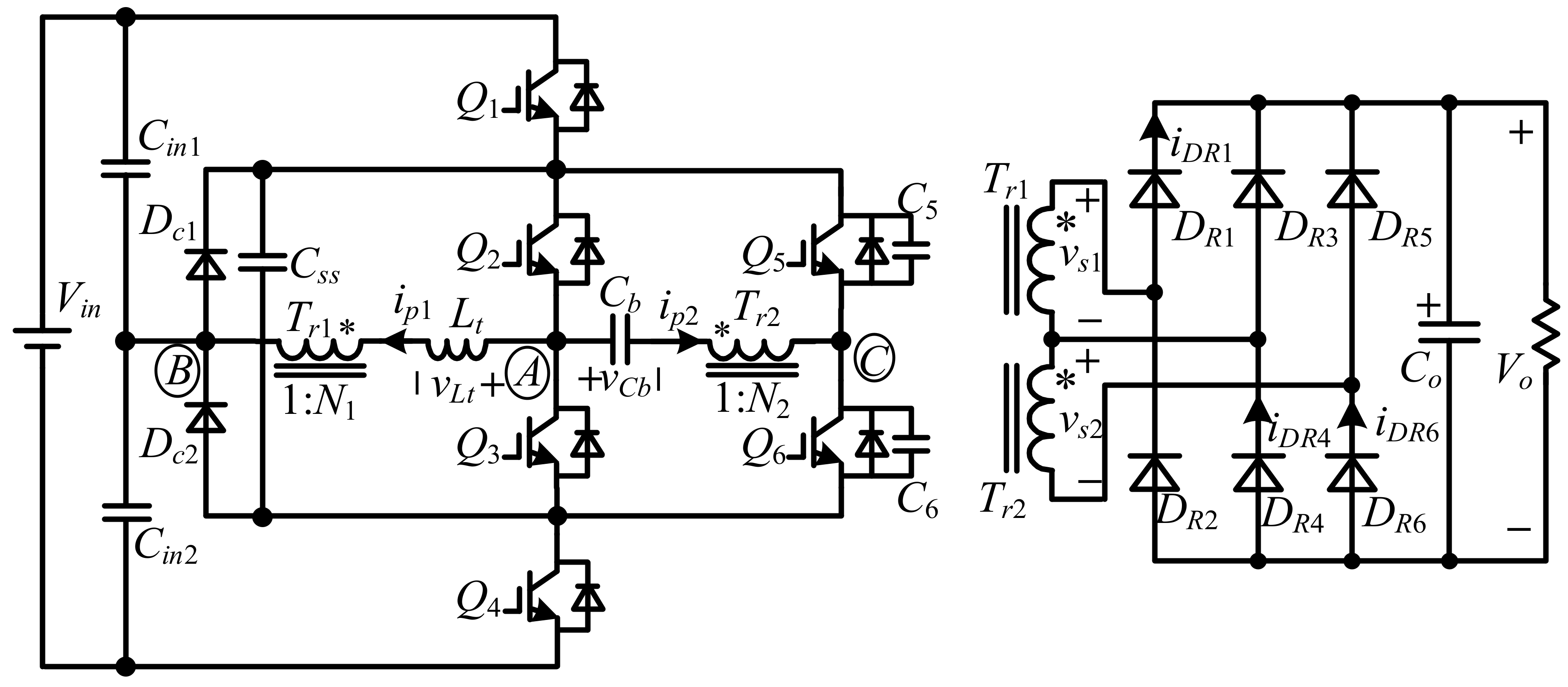
The proposed hybrid ZVZCS TL converter is shown in
Figure 1. The conventional TL unit is composed of two input divided capacitors,
Cin1 and
Cin2; four main switches,
Q1~
Q4; two clamping diodes,
Dc1 and
Dc2; a flying capacitor,
Css; a primary winding of main transformer,
Tr1; and a transmission inductor,
Lt. The auxiliary structure is composed of switches
Q5 and
Q6 (including two extra paralleled capacitors,
C5 and
C6), blocking capacitor
Cb, and primary winding of auxiliary transformer
Tr2. At the rectifier side, the secondary windings of
Tr1 and
Tr2 are connected in series, and six diodes,
DR1~
DR6, form two full-bridge rectifier cells, in which
DR1,
DR2,
DR5, and
DR6 form one rectifier cell and
DR1~
DR4 form another one.
Co is the output filter capacitor.
N1 is the turns ratio of
Tr1,
N2 is the turns ratio of
Tr2, and
N2 should be smaller than
N1 to make the converter work properly.
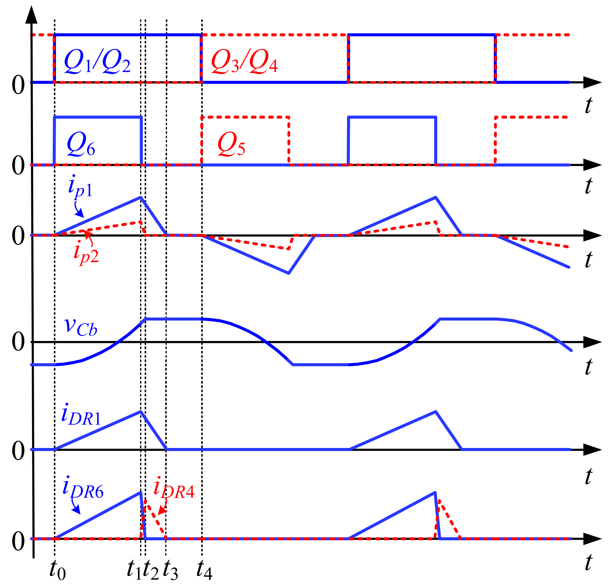
The key waveforms of the proposed converter are given in
Figure 2. The switches
Q1/Q2 and
Q3/Q4 in the three-level unit are complementarily switched at a fixed 50% duty cycle with a dead time.
Q5 and
Q6 use PWM chopping control and have the same turn-on time as
Q3 and
Q1, respectively. The
Cin1 and
Cin2 are identical and large enough so that the input voltage,
Vin, is considered constant at the steady state and identically divided by the two capacitors. Considering symmetry, a half-switching cycle over four modes was studied and is depicted in
Figure 3.
(1) Mode 1 [
t0,
t1]: At
t0,
Q3 and
Q4 are turned off, and
Q1,
Q2, and
Q6 are turned on. Due to the fact that there are no currents flowing through all switches before
t0,
Q1,
Q2, and
Q6 are turned on with the ZCS condition. As shown in
Figure 3a, active power is transferred from source to load through two transformers. At the input side, the primary current (
ip1) of transformer
Tr1 flows through
Q1,
Q2, primary winding of
Tr1,
Lt, and
Cin1; the primary current (
ip2) of transformer
Tr2 flows through
Q1,
Q2,
Cb, primary winding of
Tr2,
Q6,
Dc2, and
Cin1; and
vAB =
vAC =
Vin/2. At the output side, the current flows through the secondary windings of
Tr1 and
Tr2, and through
DR1 and
DR6. The leakage inductance of
Tr1 is involved in the transmission inductance,
Lt, and the leakage inductance of
Tr2 is represented as
Llk, which is not shown in
Figure 1. The voltages across the
Lt,
Cb, and
Llk are represented as
vLt,
vCb, and
vLlk, respectively. Therefore, the voltages of the secondary windings of
Tr1 and
Tr2, and
vs1 and
vs2, respectively, can be derived as follows:
The voltages
vLt and
vLlk can be expressed as follows:
For the blocking capacitor,
Cb, we have the following:
For the output side, we have the following:
where
iDR1 and
iDR6 are the currents flowing through
DR1 and
DR6, respectively.
Substitution of (1)~(4) into (5), and we can have the following:
At
t0, the value of
vCb is
vCb(
t0) and
ip2(
t0) = 0, and (7) can be obtained from (6):
According to the analysis, the equivalent circuit reflecting to the secondary sides of transformers is given in
Figure 4, and we have the following:
where we have the following:
(2) Mode 2 [
t1,
t2]: At
t1,
Q6 is turned off. Due to
C5 and
C6, the rise rate of the voltage across
Q6 is limited, and
Q6 achieves ZVS turn-off. When
C5 is charged to
Vin/2 and
C6 is discharged to zero, the anti-parallel diode of
Q5 naturally conducts, and
ip2 flows through it. Then
ip2 flows through
Q2, the primary winding of
Tr2,
Cb, and the anti-parallel diode of
Q5, and it should be noted that
vCb(
t1) is positive now and, thus,
ip2 will decay rapidly with the help of
vCb. At the output side, the current flowing through the secondary winding of
Tr2 also decays rapidly while the current is flowing through the secondary winding of
Tr1 almost unchanged; thus,
DR4 conducts to compensate for the reduced current of
Tr2. In other words, both
DR4 and
DR6 conduct in this mode. At
t2, both
ip2 and
iDR6 are decayed to zero; hence, the circulating currents are removed from
Q2,
Q5, and
Tr2, and
DR6 is turned off with the ZCS condition. The voltage
vCb is considered to be constant during the mode because the time interval [
t1,
t2] is very short:
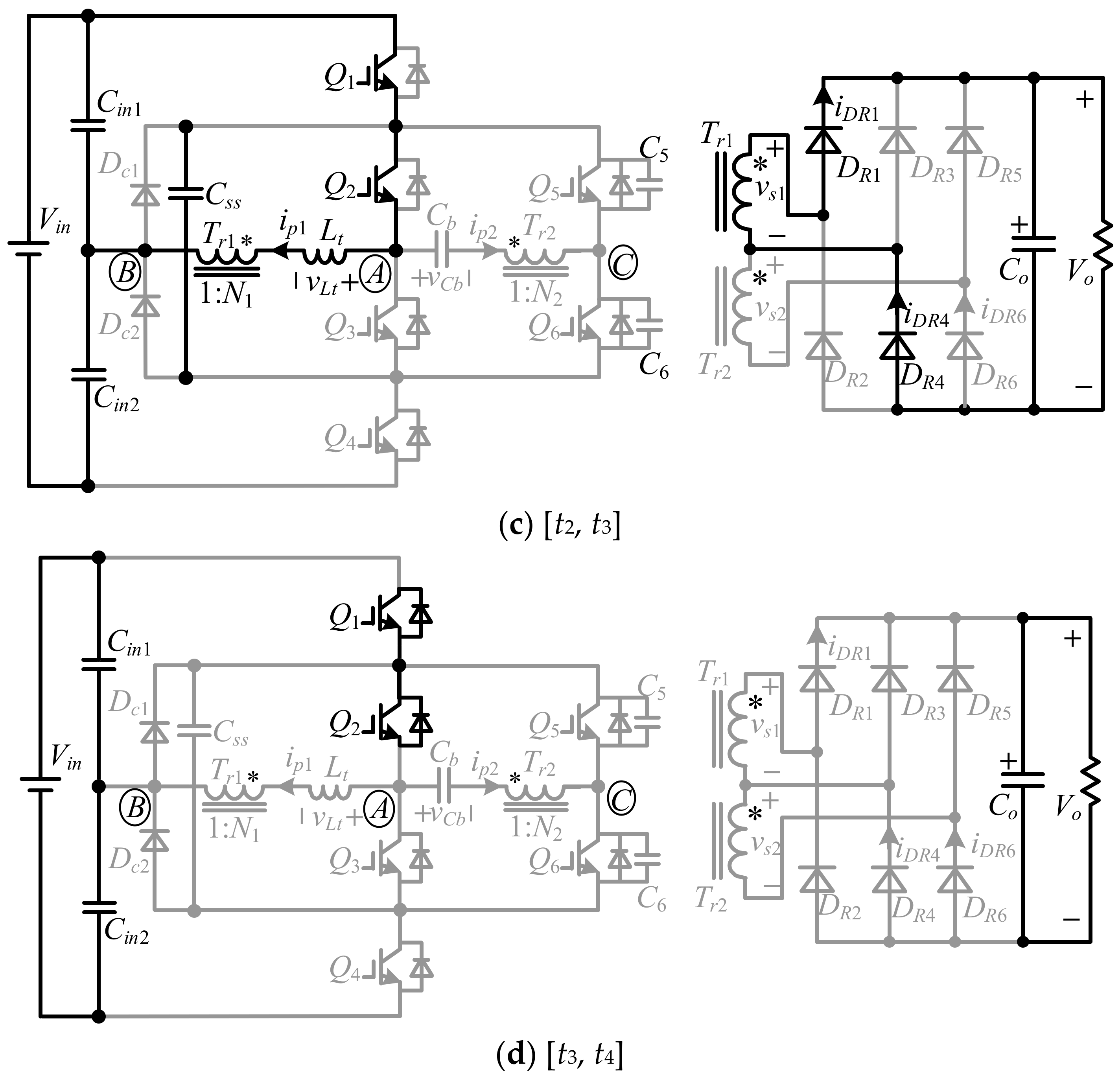
(3) Mode 3 [
t2,
t3]: As shown in
Figure 3c, the current loop of
ip1 is still the same as that in Modes 1 and 2, while at the output side, the current flows through
DR4, the secondary winding of
Tr1 and
DR1. Thus, the voltage across the secondary winding of
Tr1 is clamped at
Vo, and
ip1 has the same expression as (12), and it decreases to zero at
t3. Moreover,
vCb stays constant in this mode:
For the proper operation of the converter, Vin/2 must be lower than Vo/N1, as ip1 decays linearly in this mode.
(4) Mode 4 [
t3,
t4]: As shown in
Figure 3d, at
t3,
ip1,
iDR1, and
iDR4 decrease to zero, and
DR1 and
DR4 are turned off with ZCS. Although
Q1 and
Q2 are still ON, the voltage across the secondary winding of
Tr1 is lower than
Vo, and, thus, there is no current flowing through them, and
vCb remains unchanged in this mode. The load is only supplied by
Co. At
t4,
Q1 and
Q2 are turned off with ZCS, while
Q2,
Q3, and
Q5 are turned on with the ZCS condition. Moreover, the voltage of
Q5 equals
vCb(
t3) and is relatively lower than
Vin in this mode, meaning that
Q5 is turned on with the approximate ZVZCS condition.
According to the above analysis, it can be seen that the four main IGBT switches, Q1~Q4, realize ZCS turn-on and turn-off; and the two auxiliary IGBT switches, Q5 and Q6, realize ZVZCS turn-on and ZVS turn-off. Due to the fact that the current flowing through the auxiliary IGBTs is relatively lower than that in the main IGBTs, the switching losses of the converter can be reduced significantly, and, moreover, the circulating current in the primary side of Tr2 is also eliminated and the conduction losses of Q2, Q3, Q5, and Q6 can be reduced further.
3. Converter Design Procedure
For the convenience of design and simulation, the given parameters are as follows: input voltage, Vin, is 1500 V; output voltage, Vo, is 15 kV; rated power, PN, is 2 MW; and the switching frequency, fs, is 1000 Hz.
3.1. Capacitance of Cb
The voltage rating of the blocking capacitor, vCb(t0), is heavily dependent on the capacitance of Cb; in addition, it also determines the time interval of Mode 2 (t1~t2). It is well-known that, the larger the value of Cb, the lower the required voltage rating of Cb is; however, the longer time interval of (t1~t2) is, in other words, generating larger conduction losses in primary side switches.
According to the operation principle and
Figure 2, we have the following:
Substitute (17) into (9), and we have the following:
Normalize
Cb to
Cb_nom and
vCb(
t0) to
vCb_nom(
t0), and Equation (18) can be rewritten as follows:
where we have the following:
Obviously, the time interval of mode 1 is smaller than the half resonance cycle, which should satisfy the following:
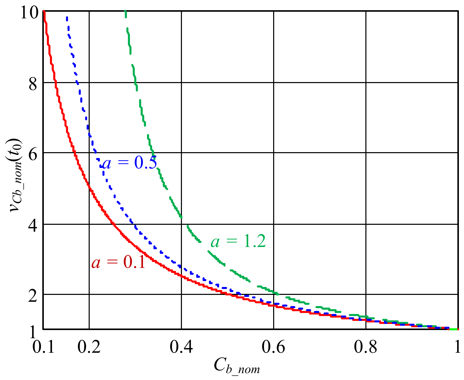
Without losing generality, three different values of
a (0.1, 0.5 and 1.2) are selected, and
vCb_nom(
t0) can be drawn versus
Cb_nom with (19), as shown in
Figure 5. It can be seen that
vCb_nom(
t0) increases with the decrease of
Cb_nom. Taking
a = 0.5, for instance, when the
Cb_nom is shrunk to 1/7, the
vCb_nom(
t0) will increase 10 times. Therefore, the
Cb should be set relatively larger to keep a smaller voltage rating.
From the analysis in
Section 2, the role of
Cb is to reset the primary current of
Tr2 to zero during the freewheeling state (
t1,
t3), and, in general, the
Cb is set to relatively larger to make the
vCb smaller enough compared with the input voltage,
Vin. Furthermore, due to the fact that the
Llk is smaller than
Lt, and
N2 is smaller than
N1 for the proper operation of the converter, according to
Figure 4, the currents of the secondary windings of
Tr1 and
Tr2 can be simplified as follows:
From (12), we have the following:
From (12) and (14), we have the following:
Combining (23) and (24) yields, the following:
Cb is always charged in Mode 1, and thus we have the following:
Moreover, the value of
Cb can be expressed by the following:
3.2. Turns Ratios N1 and N2
It was mentioned in
Section 2 that most of the converter power should be delivered by
Tr1 to reduce the switching losses through the proper design of
N1 and
N2, which is analyzed in this subsection. Only the power transmission during [
t0,
t4] is analyzed here due to the symmetry operation between two half cycles. Assuming 100% conversion efficiency of the converter and the transmission power,
Ptot, during [
t0,
t4] can be expressed by the following:
The power delivered by
Tr1 and
Tr2 is as follows:
By combining (28) and (29), we have the following:
It can be seen from (31) that
Ptr1/
Ptr2 is only determined by
N1 for the given
Vo and
Vin, and
Figure 6 is illustrated with the given parameters. It can be seen that
Ptr1/
Ptr2 increases with the increase of
N1, and without losing generality,
N1 is set to 18, and
Ptr1/
Ptr2 = 9:1, as shown in
Figure 6.
The converter should operate in the critical current continuous mode to reduce the peak current as far as possible under full load condition; in other words, there is no Mode 4:
For
Lt, the Equation (33) can be obtained by the volt–second balance rule.
Combining (32) and (33) yields the following:
where
D = (
t1 −
t0)/
Ts is the duty cycle.
Obviously,
D < 0.5, and we have the following:
Then N2 should be larger than 2 when N1 = 18.
Under full load condition,
Ptr1 can be expressed as follows:
By combining (31) and (36), we have the following:
From (38), it can be seen that, the smaller N2 is, the lower ip2(t1) is, which also is the peak current and turn-off current of Q5/Q6. Therefore, to reduce the turn-off losses of Q5/Q6, N2 should be as smaller as possible.
3.3. Transmission Inductance Lt and Llk of Tr2
Under full load condition with (22), (34), and (38), we have the following:
Figure 7 can be illustrated with (39) for the given parameters, and
N1 = 18. It can be seen that, the lower
N2 is, the smaller the
Lt is required to be. However,
Lt has a minimum inductance due to the existence of the leakage inductance of
Tr1.
From (12), we can find that the time interval of Mode 2 [t1, t2] is determined by Llk. Therefore, Llk should be designed to be as small as possible to shrink the freewheeling state to reduce the conduction losses.
5. Experimental Results
The switching process and performance of the proposed converter are experimentally verified by a hardware prototype with 150–750 V, 1 kW. The turns ratios are
N1 = 9 and
N2 = 2, inductors are
Lt = 8 μH and
Llk = 3 μH, blocking capacitor is
Cb = 10 μF, flying capacitor is
Css = 1 μF,
Q1~
Q6 are CRG60T60AK3HD,
DR1~
DR6 are RHRG30120, and switching frequency is
fs = 10 kHz. The prototype converter is shown in
Figure 9.
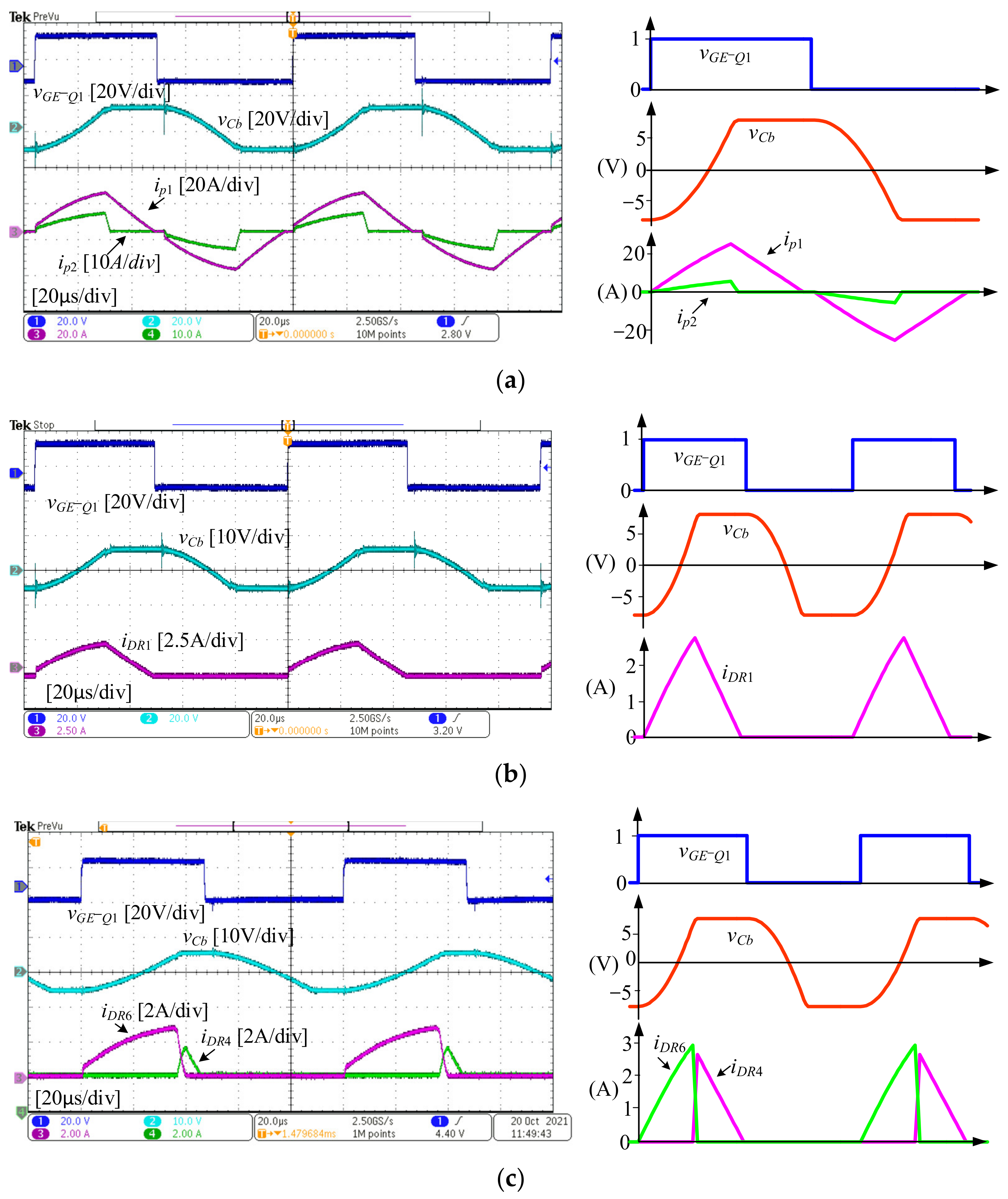
The main waveforms of the proposed three-level converter under rated power are shown in
Figure 10 and
Figure 11. For each experimental waveform, its corresponding simulation waveform is also given to verify the correction. As seen from
Figure 10a, the current of
ip2 rapidly falls to zero, while the current
ip1 slowly decays to zero before the auxiliary switches are turned off. As seen from
Figure 10b,c, all the currents flowing through the rectifier diodes linearly fall to zero without reverse recovery losses. The experimental waveforms match well with both the theoretical and simulation waveforms.
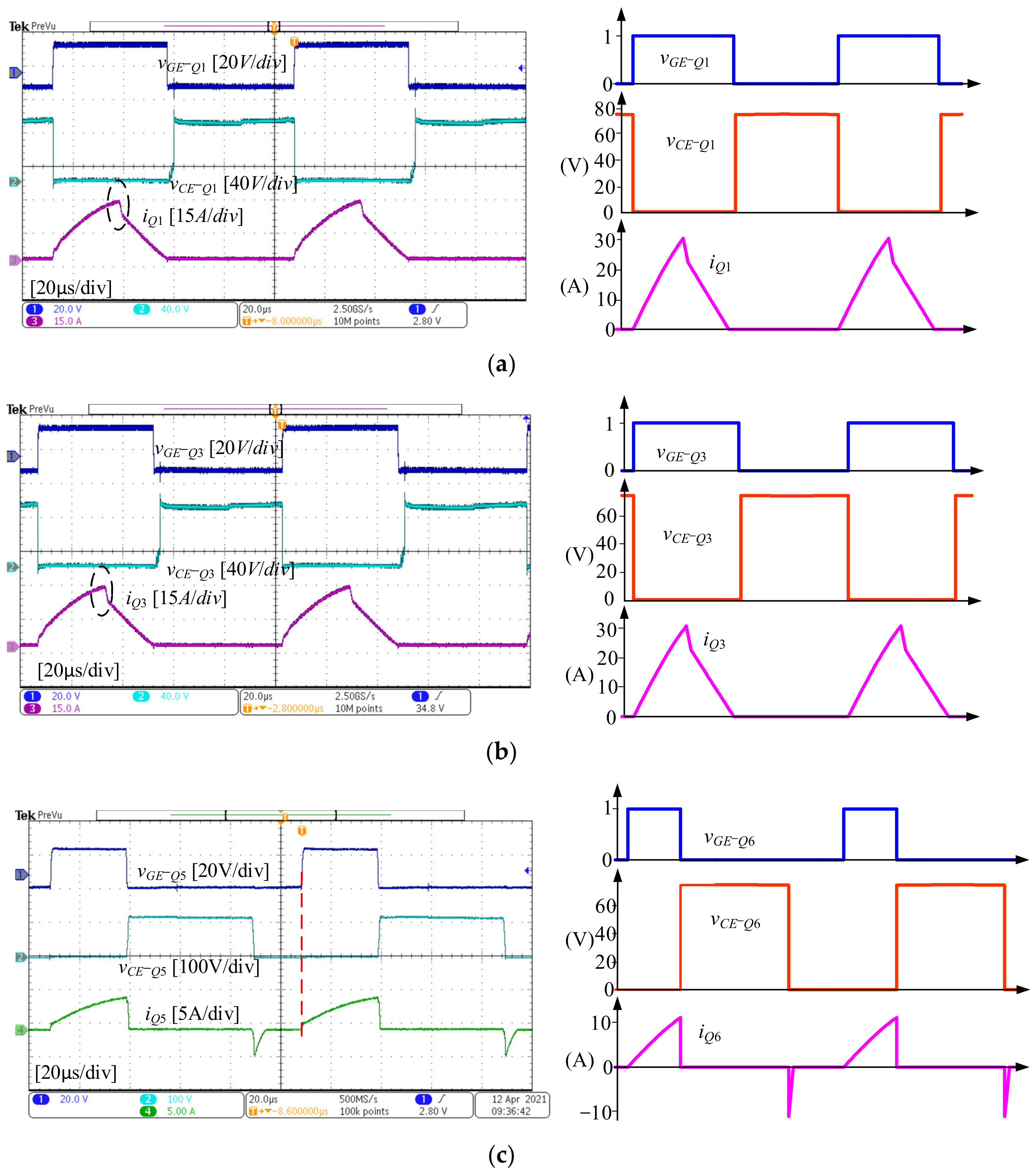
Figure 11 shows the gate–emitter voltage,
νGE; the collector–emitter voltage,
νCE; and the collector current of the switches,
Q1,
Q3, and
Q6. For the main switches,
Q1 and
Q3, they are turned on and off with ZCS condition, while for the auxiliary switch,
Q6, it is turned off with ZVS and turned on with ZVZCS condition. Since
iQ1 in Mode 1 is the sum of
ip1 and
ip2, and only
ip1 in Mode 2, there is a phenomenon of current drop, as shown in the dotted box in
Figure 11a.
Compared to Reference [
20], the remarkable feature of the proposed converter is that the primary side conduction losses of
Q2,
Q3,
Q5,
Q6, and
Tr2 are decreased due to the rapid decline of
ip2, and if
Cb,
DR3, and
DR4 are removed from the converter, the converter will have a similar operation principle to that in Reference [
20].
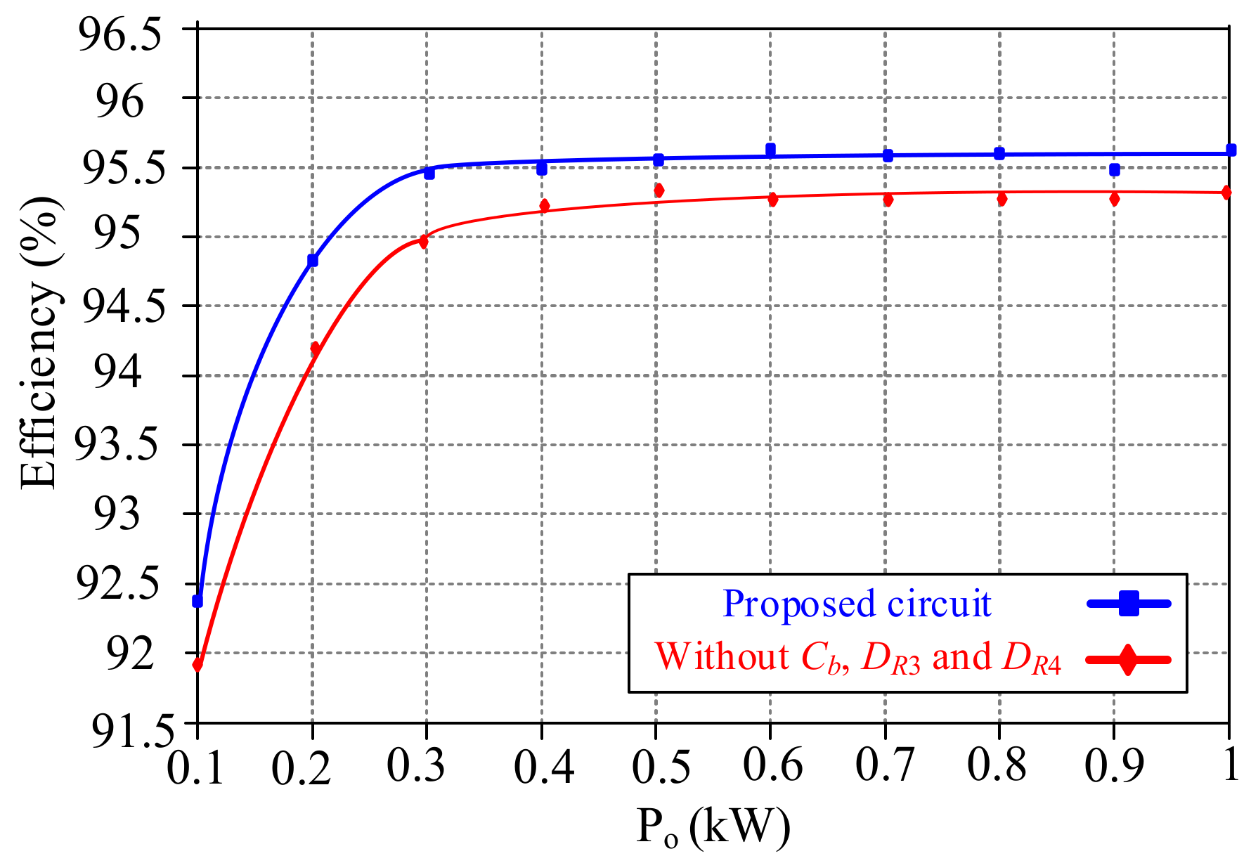
To show the advantages of the introduced blocking capacitor,
Figure 12 shows the comparison between the efficiencies of the proposed converter and that, without
Cb,
DR3, and
DR4, it is obvious that, due to the reduced conduction losses of
Q2,
Q3,
Q5,
Q6, and
Tr2, the proposed converter has a higher efficiency.


