Abstract
Classical thermal rectification arises from the contact between two dissimilar bulk materials, each with a thermal conductivity (k) with a different temperature dependence. Here, we study thermal rectification in a Si(1−x)Gex alloy with a spatial dependence on the atomic composition. Rectification factors (R = kmax/kmin) of up to 3.41 were found. We also demonstrate the suitability of such an alloy for logic gates using a thermal AND gate as an example by controlling the thermal conductivity profile via the alloy composition. This system is readily extendable to other alloys, since it only depends on the effective thermal conductivity. These thermal devices are inherently advantageous alternatives to their electric counterparts, as they may be able to take advantage of otherwise undesired waste heat in the surroundings. Furthermore, the demonstration of logic operations is a step towards thermal computation.
1. Introduction
The understanding of heat propagation and the tunability of the thermal properties of materials is a topic of active research motivated by the increasing importance of thermal management and energy-efficient devices [1,2,3]. In that regard, concepts such as: thermal transistors, diodes, and memories [4,5,6,7,8,9,10,11] have emerged. While heat dissipation is typically considered an obstacle to faster electronics, these developments have positioned heat current to serve as a promising alternative candidate for realizing logic operations using relatively simple device configurations with an easily measurable variable, such as the temperature, especially in situations in which heat may be readily available as an energy source. The realization of thermal components that control heat flow at the nanoscale in a manner similar to that of electronics could enable thermal analogs of electronic circuits [12,13,14,15,16]. Thermally driven logic operations have an inherent advantage in that thermal computers can potentially utilize any waste heat from the surroundings. Examples of this concept have already been demonstrated by taking advantage of waste heat from industrial fume hoods [17], volcanoes [18], and vehicle exhaust gas [19,20], to name a few. In many of the aforementioned scenarios, as well as other situations such as space exploration or geothermal energy exploration in the earth [13], in which elevated temperatures are encountered, thermally based logic circuits and computations possess a key advantage, as electronics face a severe degradation in device performance at high temperatures [21].
Within this context, thermal rectification is a useful phenomenon for thermal management, which serves as an essential building block for thermal logic circuits in conjunction with thermal diodes [22]. Thermal rectification can be defined as an asymmetric and nonlinear process in which the thermal properties of the material along a specific axis depend on the direction of the temperature gradient or the heat current [23]. In solids, several mechanisms for thermal rectification have been previously proposed, such as: differing thermal boundary resistances between two materials [24,25,26], anharmonic interatomic potentials [27], a difference in the temperature dependence of the thermal conductivity of two connected dissimilar bulk materials [28,29,30], and asymmetrically structured materials (including: load mass [31], ballistic scattering [32], asymmetric nonlinear radiation [33], and mass gradient [34,35,36]). Traditional materials and designs for thermal rectification are based on the different temperature dependences of the thermal conductivities of different bulk materials that are brought together.
In this work, we consider the mass gradient mechanism to study thermal rectification in alloy-based 1D slab structures in which the alloy composition is graded along the length of the material [37,38,39]. By continuously changing the material composition (x, i.e., the atomic percent) along a specific axis (see Figure 1 and Figure 2), we designed a theoretical slab with a thermal conductivity that depends on temperature and space, allowing for control of the heat flux across the slab. We incorporated five different mass distributions based on: linear, quadratic, exponential, Gaussian, and Fermi-like functions. An estimated rectification coefficient, R, of 3.41 was determined for a temperature difference of ΔT = 600 K in Si(1−x)Gex, with the material concentration varying from 0 < x < 0.6 for a Fermi-like mass distribution. This value represents one of the highest rectification factors using graded materials [14]. While the thermal bias required to achieve such a rectification factor appears to be quite large, thermal gradients up to 700 K have been experimentally probed in pristine [40] and patterned [6,41] silicon nanomembranes. Large temperature gradients have also been demonstrated in silicon nanowires [42]. Even in atomically thin few-layer MoSe2, thermal gradients of 400 K have been reported [43]. We build upon this idea and demonstrate how grading of the alloy and subsequent control of the thermal conductivity profile enables the creation of a thermal AND gate.

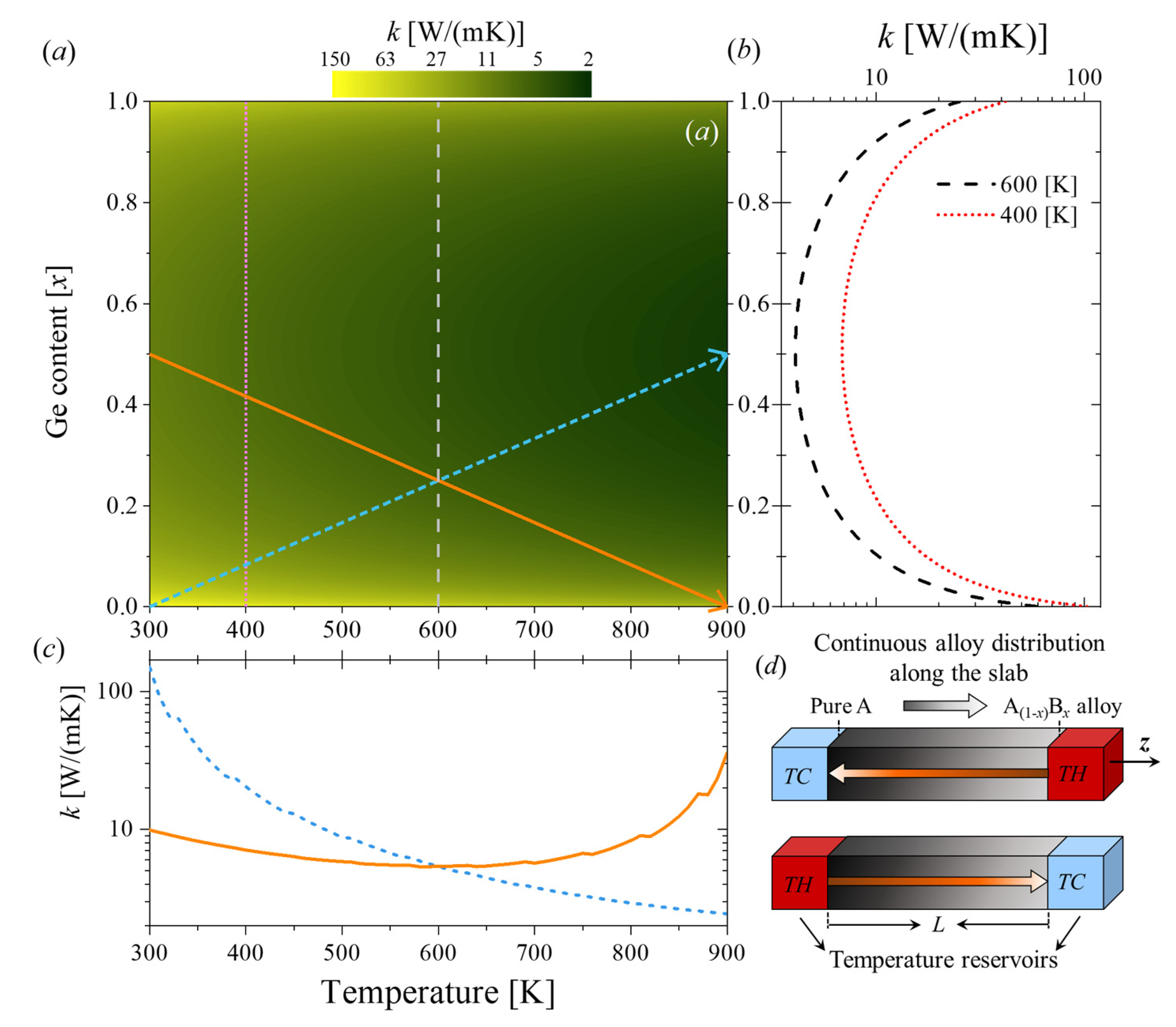
Figure 1.
(a) Contour plot of the thermal conductivity (k) of Si(1−x)Gex alloy as a function of Ge content (x) and temperature (green contour). Four different “cuts” of the contour taken, as indicated by the colored lines (b), two vertical cuts at T = 400 and 600 K (dotted magenta and dotted grey lines, respectively), and (c) two diagonal cuts (solid orange and dotted blue lines). (b) Thermal conductivity of Si(1−x)Gex as a function of Ge content at a fixed temperature T = 400 and 600 K (dotted red and dashed black lines, respectively). (c) Thermal conductivity as a function of temperature of a Si(1−x)Gex slab where the Ge content varies linearly along the slab between x = 0 (pure silicon, Si) and x = 0.5 (Si0.5Ge0.5). It should be noted that this spatial dependence creates different k curves when the temperature reservoirs are changed. (d) Schematic representation of the continuous alloy distribution along the heat flux axis (z) of a hypothetical slab of alloy of length L for the cold-hot (forward) and hot-cold (reverse) configurations.
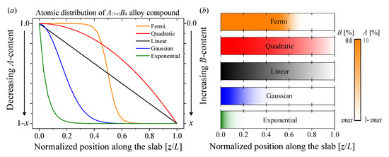
Figure 2.
(a) Spatial atomic distribution of B (or A) atoms along the A(1−x)Bx alloy slab. (b) Schematic representation of the variation in the atomic content along the slab. The color scale represents the amount of A atoms in the A(1−x)Bx alloy slab. The color bar is valid for all of the slabs for their respective colors.
We first introduce the theoretical model and associated equations. Then, we study the effect of the different mass distributions and determine the best configuration to obtain the highest rectification factor. Finally, as proof of concept, we use the mass distribution concept to create an AND logic gate. All simulations were performed with finite element model (FEM) simulations performed with the commercially available COMSOL multiphysics v.5.1 software. The COMSOL parameters used for the thermal properties of the materials in this work are summarized in the Supporting Information in Table S1.
2. Materials and Methods
Figure 1a is a contour plot that gives the thermal conductivity as a function of the Ge concentration and the temperature, which shows how the thermal conductivity profile can be controlled. The vertical magenta and grey cuts in Figure 1a indicate a constant temperature of 400 [K] and 600 [K], respectively, and their alloy distributions across the slab and the associated thermal conductivity profiles are highlighted in Figure 1b. Figure 1c shows the thermal conductivity profiles of diagonal cuts taken from Figure 1a, which correspond to a graded alloy rectifier (Figure 1d), where the dotted blue cut corresponds to a rectifier in the cold-hot (forward) rectification configuration, while the solid orange cut corresponds to a rectifier in the hot-cold (reverse) configuration. We note that despite having a variation between a concentration of x = 0 (pure silicon) and x = 0.5 (Si0.5Ge0.5), the configuration of the temperature reservoirs changes the spatial dependence of the thermal conductivity. In this manner, the thermal conductivity profile and the rectification properties of the alloy material can be controlled by grading the alloy across a slab. The spatial dependence of the thermal conductivity and the mathematical expressions that describe them are presented in Figure S1 in the Supporting Information and in Equations (1)–(5).
If a finite temperature gradient, ΔT, is established in a material, the rate of heat energy flow, Q, at steady state is given by the expression:
where k is the thermal conductivity. The rectification factor of Si(1−x)Gex was calculated with a power-law dependence of the thermal conductivity on temperature and material composition. It is well known that for semiconductors, the temperature dependence of k can be modeled by a simple power law [44,45]:
where k300 is the value of the thermal conductivity of the semiconductor at T = 300 [K], and α is a constant. This approach typically shows good agreement with experimental data over a large temperature range from 300 K < T < 900 [K]. For the case of alloy materials of type A(1−x)Bx, thermal conductivity values vary between kA and kB (i.e., the thermal conductivity values of pure A or pure B), though a dramatic decrease is observed in alloys relative to the pure crystals (see Figure 1b). This effect is mainly attributed to strong alloy scattering of high-frequency phonons as a result of a break in the perfect periodicity of the otherwise pure structure. Similar to the pure crystal case, the thermal conductivity of the alloy material, kAB, can also be expressed by a simple power law given by [44,45]:
where kAB(x) can be expressed as a quadratic interpolation given by Norbury’s rule [46,47,48,49]:
where CAB is a constant that accounts for the contribution of the lattice disorder generated in the alloy due to the random distribution of the atoms in a sublattice. This term is usually called a bowing or nonlinear parameter. More detailed descriptions of Equations (2)–(5) are found in the works of Palankovski [44,45] and Adachi [47,48,49].
Once the thermal conductivity expression is defined, thermal rectifiers are created by continuously varying the amount of the B atom in the alloy along the main axis of the thermal flux in the z-direction, as displayed in Figure 1d. The continuous alloying causes the effective k to depend on the configuration of the temperature reservoirs, shown in Figure 1c. The rectification factor, R, can be used as a figure of merit to quantify the performance of a thermal rectifier. While it possesses several different definitions in the literature [14], it is always based on a ratio of the effective thermal conductivities measured in two different configurations of the thermal bias. Here, we use the following definition for the thermal rectification:
where kf and kr are the effective thermal conductivities measured in cold-hot, TC-TH (forward, f), and hot-cold, TH-TC (reverse, r), configurations of the temperature reservoirs, respectively. The effective thermal conductivity is obtained by integration over its spatial dependence for both the forward and reverse reservoir configurations. R is a relevant figure of merit, as it provides a quantification of the heat flux in the forward direction relative to that in the reverse direction, in a manner analogous to that of an electrical rectifier.
The ability to control the thermal conductivity as a function of alloy content allows for the creation of thermal-based logic gates. Logic gates can be characterized according to a truth table, in which a combination of high or low inputs results in a specific output. Here, we define the effectiveness ε of our thermal-based logic gate as:
where Tout is the output temperature detected at the center of the slab, Tground is the temperature of the ground (TC), and ΔT is the thermal bias (i.e., the temperature difference between the high and low temperatures, ΔT = TH-TC). The most effective operation of an AND gate occurs when the device operates as close to 1–0 as possible (i.e., ε should be as close as possible to 0 for a low output and as close as possible to 1 for a high output).
3. Results
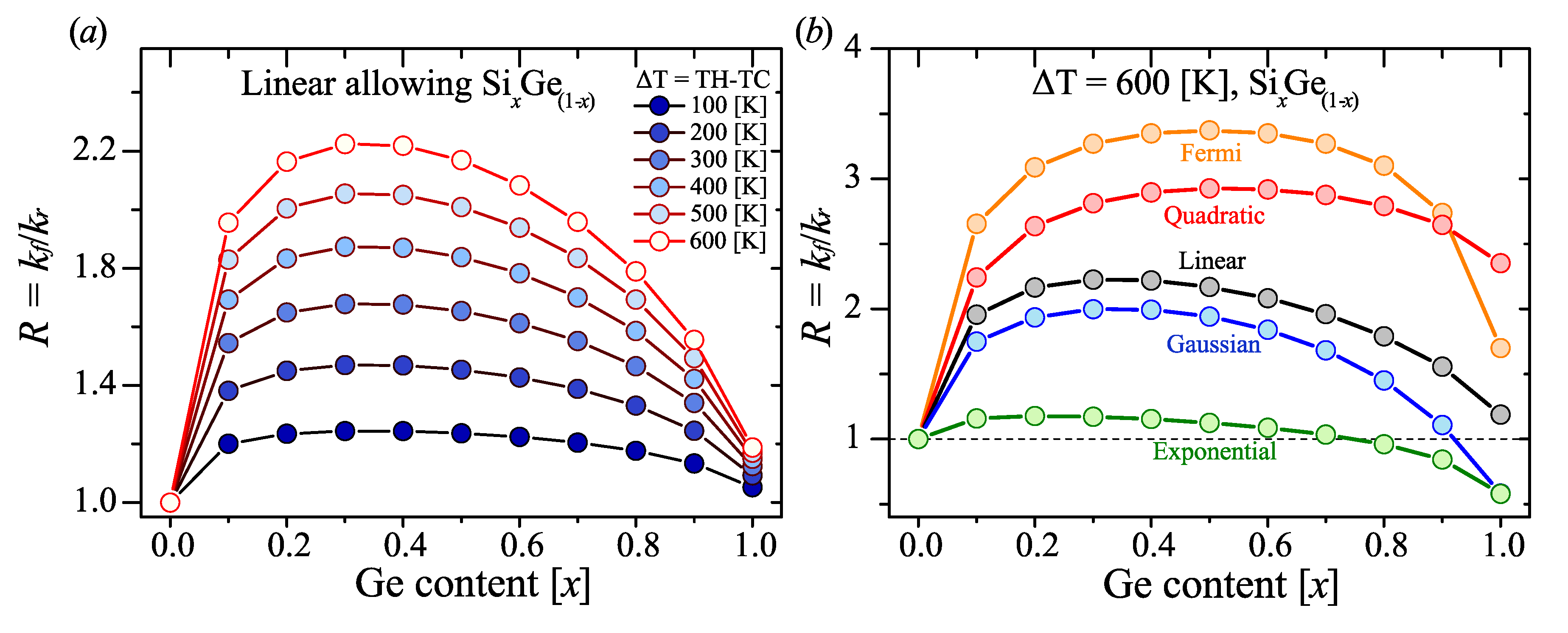
The rectification factors were calculated for five different spatial distributions (linear, quadratic, exponential, Gaussian, and Fermi-like) of “B” (or “A”) atoms along the main axis of the thermal flux of an A(1−x)Bx alloy slab. We define z to be the position along the length of an alloy slab of length L. The spatial distributions used in this work are displayed in Figure 2a and are schematically illustrated in Figure 2b. As an example, we examined the dependence of R with respect to the thermal bias ΔT in a Si(1−x)Gex slab and the associated spatial distribution along the slab. We also present a comparison with other alloys for a linear distribution in the Supporting Information (Figures S2 and S3a), which qualitatively follow the same trend for the results that we observe here, meaning that these results can be readily extended to other graded alloy materials. The ΔT was generated by keeping the cold reservoir at a constant T = 300 [K] and varying the hot reservoir from 400 to 900 [K]. Rather than grading the slab from pure silicon to pure germanium, we fixed one end of the slab with pure Si, while the other end had varying amounts of Ge, as set by x, with the alloy composition between these ends being graded according to the given distribution. In other words, the Ge content (x) was varied along z from 0 < x < xmax, where 0 < xmax < 1. Finally, the rectification factor was obtained by applying Equation (6) using the effective thermal conductivities calculated in both the forward and reverse configurations of the temperature reservoirs.
Figure 3a shows R as a function of Ge content with varying ΔT. The Ge content was varied linearly, as indicated by the solid black line in Figure 2a and the black graded slab in Figure 2b. A maximum R ~ 2.2 was obtained for Ge content varying linearly between 0 < x < 0.3 at ΔT = 600 [K], since kAB scales vary with the temperature according to Norbury’s rule. We note that this range of Ge results in the maximum R for all ΔT as the thermal conductivity drops dramatically in this range (Figure 1b). We then extended this analysis to incorporate this maximum ΔT of 600 [K] and studied different spatial distributions of Ge atoms. The temperature dependence of R for the different linear Ge distributions is also shown in Figure S3b in the Supporting Information. From this figure, we can observe that the R factor increases monotonically with ΔT. Figure 3b compares five spatial distributions as a function of Ge content at fixed ΔT = 600 [K]. A Fermi-like distribution of Ge atoms gives us the maximum R = 3.37 for Ge content varying from 0 < x < 0.5. Another interesting feature of Figure 3b is that for exponential and Gaussian-like distributions of Ge content, R drops below 1 for x > 0.8 and x > 0.9, respectively, as the effective thermal conductivity becomes larger in the reverse configuration (TH–TC) than in the forward one (TC–TH). The thermal conductivity and the temperature distribution as a function of z for the studied distributions are displayed in Figure S1 in the Supporting Information.
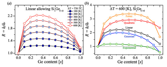
Figure 3.
(a) Rectification factor as a function of Ge content for varying thermal bias (ΔT), with Ge linearly distributed along the Si(1−x)Gex alloy slab. (b) R as a function Ge content for the different distributions of Ge atoms along the alloy slab at fixed ΔT = 600 [K].
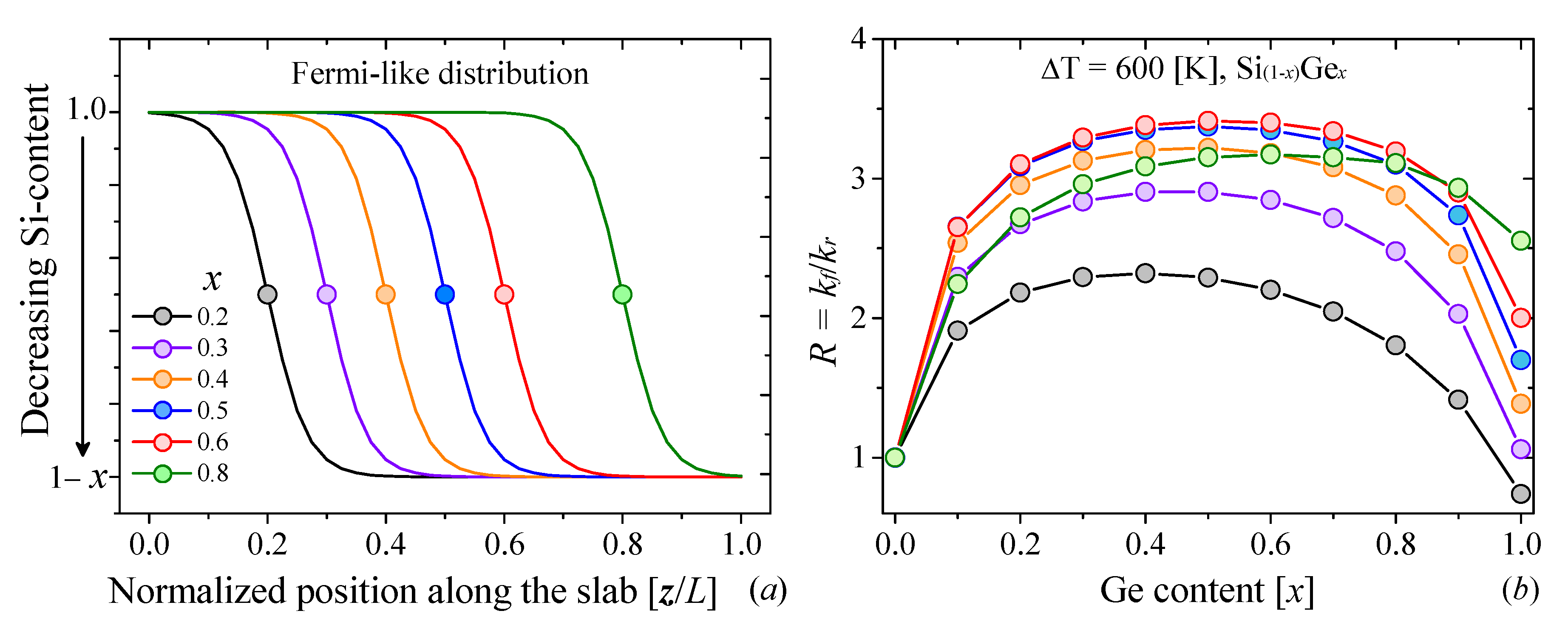
We considered the Fermi distribution more carefully, as it yielded the highest values of R across all of the distributions. As before, the Ge content (x) was varied along z from 0 < x < xmax, where 0 < xmax < 1. Figure 4a shows the spatial alloy distribution for slabs with varying alloy compositions. Each color indicates the value of x for the given slab. The point at which the Fermi-like spatial distribution reaches the half-point in atomic percent between the compositions at each end of the slab is indicated by a solid dot for each slab. This point is important, as it is a parameter that we set in our Fermi-like distribution that affects how the slab is graded (see Supporting Information). Figure 4b then shows the associated R for each of these slabs as a function of position along the slab at ΔT = 600 [K]. The same qualitative behavior is observed for the Fermi-like distribution for all compositions as in Figure 3b, with the highest R factors occurring for alloyed materials (i.e., non-pure materials) due to the decrease in thermal conductivity resulting from alloy scattering of thermal phonons, as explained previously. In general, the highest R values occur for alloys that have higher concentrations of Ge, with an optimal at x = 0.6. In this case, a value as high as R = 3.41 is observed. It is worth noting that similar values were found by Shih et al. [50], where the maximal R for idealized bi-segment thermal rectifiers was studied. They derived an upper limit of R = 3 for rectifiers whose k varied linearly with respect to the temperature. Similarly, Figure S1f in the Supporting Information shows the approximately linear behavior of k for a Fermi-like distribution and for z/L > 0.6. Compared to more similar designs, Carlomagno et al. [51] recently found a theoretical rectification factor as high as 2.77 using graded Si1−xGex wires that were linearly distributed along the wires. However, more notably, among thermal rectification designs that are based on a conduction mechanism, our design exhibits one of the highest R values while also being physically realizable to fabricate and implement [14,37,51,52].
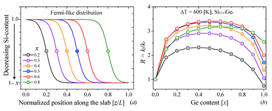
Figure 4.
(a) Fermi-like spatial distribution of Si (or Ge) atoms along the length of the Si(1−x)Gex alloy slab (z). The color scale represents varying values of x. The solid dots represent the half-point of the Fermi-like distribution in x. (b) Rectification factor as a function of the position along the slab for alloy slabs of varying composition presented in (a). The color scheme is consistent throughout the figure.
Finally, we demonstrate how such an alloy distribution can also be applied to create logic gates by demonstrating a thermal AND gate as an example. A thermal rectifier based on the Si(1−x)Gex alloy is connected to a heat sink ground at a fixed temperature of 300 [K]. The rectifier has ΔT = 600 [K], with one end fixed at 900 [K] (high input, i.e., 1) and the other end fixed at 300 [K] (low input, i.e., 0). The temperature, Tout, is detected at the center of the slab, that is, at the z at which the heat sink is connected to the rectifier by a low thermal conductivity connector. The slab here has a total length of 45 μm, though this length is arbitrary. We designed the slab such that the thermal conductivities are high at the ends and at the center where the temperature is measured and lower between these key points. The thermal conductivities are controlled by variations in the composition of the alloy across the slab via the power law and Norbury’s rule. The thermal conductivity and temperature distributions for such a slab are shown in Figure 5. Then, we can calculate ε via Equation (7) and reconstruct the AND-gate truth table. An AND gate produces a low output only when both inputs are low (e.g., 0-0, 1-0, or 0-1 input); otherwise, it produces a high output. The fixed temperatures at each end along with the Tout at the ground are summarized in Table 1, along with its associated truth table. We note that for inputs of 0 and 1, 1 and 0, or 0 and 0, our output is low (0.287 or 0), while for an input of 1 and 1, our output is high (0.8727). This is in line with the best-case low output recently reported by Pal and Puri [22], who provided the first demonstration of a thermal AND gate by using a graphene nanoribbon thermal diode, with low output effectivities reported between 0.275 and 0.5. Recently, Hamed and Ndao experimentally demonstrated NanoThermoMechanical AND and OR gates [13]. They showed low output effectivities for the AND gate ranging from 0.18 to 0.11 using high input temperatures between 900 and 1500 K. We compare the low output for a Si(1−x)Gex alloy in Figure S4 and for pure Si and pure Ge in Tables S2 and S3, respectively, in the Supporting Information. As a comparison, the low ε for a Si-based electronic AND gate is ε = 0.12 [22]. Thus, we effectively demonstrated the creation of an AND logic gate in our graded alloy system on par with other existing designs in the literature. We note that the pure Si and Ge AND gates also exhibit a 1-1 high output of ε = 0.975 and ε = 0.974, respectively. However, the low output is less ideal, exhibiting much higher values than the alloy with ε = 0.323 and ε = 0.321, respectively. The improved high output results from the higher thermal conductivity of the pure slabs, which leads to a higher average temperature at the sensing position in which the temperature is measured. However, this same effect also induces a greater low output for the 1-0 or 0-1 conditions in the pure material, which is not the case for the alloy due to the unique thermal conductivity distribution.
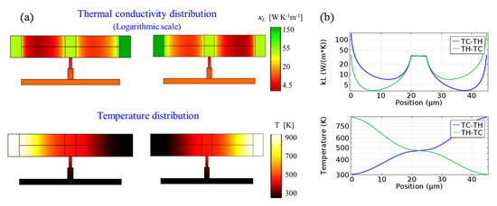
Figure 5.
(a) Thermal conductivity (top) and temperature (bottom) distribution (color scale) for the designed AND gate. One end is held at high temperature (high input), while the other end is held at low temperature (low input). The center region is connected to a heat sink via a low thermal conductivity connector. The thermal conductivity at each position along the slab is controlled by grading the alloy. The ends and center at which the temperature is measured have a high thermal conductivity. (b) Associated plots indicating the exact thermal conductivity and temperature distributions across the slab for the forward and reverse configurations. The exact position on the axis is arbitrary since we consider normalized position.

Table 1.
AND gate based on thermal rectifier and resulting truth table. The temperature is fixed at a high temperature of 900 K (high input, 1) or a low temperature of 300 K (low input, 0). The output, ε, is calculated, demonstrating that a high output only occurs when both of the inputs are high. Other logic gates can be created using a similar strategy to that employed here.
4. Conclusions
In this work, we present an extension of classical thermal rectification via the mass gradient mechanism in which we continuously grade alloy composition across a material, rather than combining different materials at an interface. We explored five spatial atomic distributions over the length of the slab and demonstrated how, in doing so, we can spatially control the thermal conductivity (and thereby the rectification factor). With a ΔT of 600 [K] in a Si(1−x)Gex alloy, we find a maximum R of 3.41 for a Fermi-like alloy distribution, one of the highest values reported based purely on a conduction mechanism. As the thermal rectification coefficient is dependent on the difference in thermal conductivities, a more drastic and abrupt change in Ge content along the thermal bias results in a much greater thermal rectification coefficient. This abrupt change induces a large asymmetry in the spatial dependence of k and, consequently, a larger rectification effect, as was demonstrated in the Fermi-like distribution. We utilized this alloy material to demonstrate how logic gates can be formed with these thermal rectifiers by demonstrating an AND gate. This concept can be readily extended to form other logic gates via thermal rectification as well.
Supplementary Materials
The following supporting information can be downloaded at: https://www.mdpi.com/article/10.3390/en15134685/s1. Table S1: Summary of COMSOL parameters; Table S2: Truth table for an AND-gate based on a pure Si slab; Table S3: Truth table for an AND-gate based on a pure Ge slab; Figure S1: Temperature and thermal conductivity distributions along a Si(1−x)Gex slab for different spatial atomic distributions; Figure S2: Thermal conductivity distributions in various alloy systems; Figure S3: Comparison of rectification in various alloy systems; Figure S4: Comparison of the effectiveness as x is varied.
Author Contributions
R.C.N.: validation, visualization, formal analysis, investigation, data curation, writing—original draft preparation, and writing—review and editing; A.C.-A.: conceptualization, funding acquisition, methodology, and software; C.M.S.-T.: conceptualization, visualization, supervision, validation, project administration, and funding acquisition; E.C.-Á.: conceptualization, visualization, formal analysis, investigation, methodology, software, validation, data curation, writing—original draft preparation, and writing—review and editing. All authors have read and agreed to the published version of the manuscript.
Funding
We acknowledge the support from Spanish MICINN project SIP (PCG2018-101743-B-100). R.C.N. acknowledges funding from the EU-H2020 Research and Innovation Programme under the Marie Sklodowska Curie Individual Fellowship (Grant No. 897148). A.C.-A. acknowledges the support from the Fondecyt Iniciación 11200620.
Institutional Review Board Statement
Not applicable.
Informed Consent Statement
Not applicable.
Data Availability Statement
Data available from the corresponding author, E.C.-Á., upon reasonable request.
Conflicts of Interest
The authors declare no conflict of interest. The funders had no role in the design of the study; in the collection, analyses, or interpretation of data; in the writing of the manuscript; or in the decision to publish the results.
References
- Qiu, L.; Zhu, N.; Feng, Y.; Michaelides, E.E.; Żyła, G.; Jing, D.; Zhang, X.; Norris, P.M.; Markides, C.N.; Mahian, O. A review of recent advances in thermophysical properties at the nanoscale: From solid state to colloids. Phys. Rep. 2020, 843, 1–81. [Google Scholar] [CrossRef]
- Qiu, L.; Scheider, K.; Radwan, S.A.; Larkin, L.S.; Saltonstall, C.B.; Feng, Y.; Zhang, X.; Norris, P.M. Thermal transport barrier in carbon nanotube array nano-thermal interface materials. Carbon 2017, 120, 128–136. [Google Scholar] [CrossRef]
- Qiu, L.; Zhang, X.; Guo, Z.; Li, Q. Interfacial heat transport in nano-carbon assemblies. Carbon 2021, 178, 391–412. [Google Scholar] [CrossRef]
- Ben-Abdallah, P.; Biehs, S.-A. Near-field thermal transistor. Phys. Rev. Lett. 2014, 112, 044301. [Google Scholar] [CrossRef] [PubMed] [Green Version]
- Li, B.; Wang, L.; Casati, G. Thermal diode: Rectification of heat flux. Phys. Rev. Lett. 2004, 93, 184301. [Google Scholar] [CrossRef] [Green Version]
- Kasprzak, M.; Sledzinska, M.; Zaleski, K.; Iatsunskyi, I.; Alzina, F.; Volz, S.; Sotomayor Torres, C.M.; Graczykowski, B. High-temperature silicon thermal diode and switch. Nano Energy 2020, 78, 105261. [Google Scholar] [CrossRef]
- Martínez-Pérez, M.J.; Fornieri, A.; Giazotto, F. Rectification of electronic heat current by a hybrid thermal diode. Nat. Nanotechnol. 2015, 10, 303–307. [Google Scholar] [CrossRef] [Green Version]
- Wang, L.; Li, B. Thermal memory: A storage of phononic information. Phys. Rev. Lett. 2008, 101, 267203. [Google Scholar] [CrossRef] [Green Version]
- Elzouka, M.; Ndao, S. Near-field NanoThermoMechanical memory. Appl. Phys. Lett. 2014, 105, 243510. [Google Scholar] [CrossRef]
- Kubytskyi, V.; Biehs, S.-A.; Ben-Abdallah, P. Radiative bistability and thermal memory. Phys. Rev. Lett. 2014, 113, 074301. [Google Scholar] [CrossRef]
- Shrestha, R.; Luan, Y.; Luo, X.; Shin, S.; Zhang, T.; Smith, P.; Gong, W.; Bockstaller, M.; Luo, T.; Chen, R.; et al. Dual-mode solid-state thermal rectification. Nat. Commun. 2020, 11, 4346. [Google Scholar] [CrossRef] [PubMed]
- Wang, L.; Li, B. Thermal Logic Gates: Computation with Phonons. Phys. Rev. Lett. 2007, 99, 177208. [Google Scholar] [CrossRef] [PubMed] [Green Version]
- Hamed, A.; Ndao, S. NanoThermoMechanical AND and OR Logic Gates. Sci. Rep. 2020, 10, 2437. [Google Scholar] [CrossRef] [PubMed] [Green Version]
- Wong, M.Y.; Tso, C.Y.; Ho, T.C.; Lee, H.H. A review of state of the art thermal diodes and their potential applications. Int. J. Heat Mass Transf. 2021, 164, 120607. [Google Scholar] [CrossRef]
- Ben-Abdallah, P.; Biehs, S.-A. Towards Boolean operations with thermal photons. Phys. Rev. B 2016, 94, 241401. [Google Scholar] [CrossRef] [Green Version]
- Hamed, A.; Elzouka, M.; Ndao, S. Thermal calculator. Int. J. Heat Mass Transf. 2019, 134, 359–365. [Google Scholar] [CrossRef]
- Casi, Á.; Araiz, M.; Catalán, L.; Astrain, D. Thermoelectric heat recovery in a real industry: From laboratory optimization to reality. Appl. Therm. Eng. 2021, 184, 116275. [Google Scholar] [CrossRef]
- Berlanga-Labari, C.; Catalán, L.; Palacio, J.F.; Pérez, G.; Astrain, D. Corrosion Behavior in Volcanic Soils: In Search of Candidate Materials for Thermoelectric Devices. Materials 2021, 14, 7657. [Google Scholar] [CrossRef]
- Hilmin, M.N.H.M.; Remeli, M.F.; Singh, B.; Affandi, N.D.N. Thermoelectric power generations from vehicle exhaust gas with TiO2 nanofluid cooling. Therm. Sci. Eng. Prog. 2020, 18, 100558. [Google Scholar] [CrossRef]
- Ximinis, J.; Massaguer, A.; Pujol, T.; Massaguer, E. Nox emissions reduction analysis in a diesel Euro VI Heavy Duty vehicle using a thermoelectric generator and an exhaust heater. Fuel 2021, 301, 121029. [Google Scholar] [CrossRef]
- Wehmeyer, G.; Yabuki, T.; Monachon, C.; Wu, J.; Dames, C. Thermal diodes, regulators, and switches: Physical mechanisms and potential applications. Appl. Phys. Rev. 2017, 4, 41304. [Google Scholar] [CrossRef] [Green Version]
- Pal, S.; Puri, I.K. Thermal AND Gate Using a Monolayer Graphene Nanoribbon. Small 2015, 11, 2910–2917. [Google Scholar] [CrossRef] [PubMed]
- Roberts, N.A.; Walker, D.G. A review of thermal rectification observations and models in solid materials. Int. J. Therm. Sci. 2011, 50, 648–662. [Google Scholar] [CrossRef] [Green Version]
- Rogers, G.F.C. Heat transfer at the interface of dissimilar metals. Int. J. Heat Mass Transf. 1961, 2, 150–154. [Google Scholar] [CrossRef]
- Powell, R.W.; Tye, R.P.; Jolliffe, B.W. Heat transfer at the interface of dissimilar materials: Evidence of thermal-comparator experiments. Int. J. Heat Mass Transf. 1962, 5, 897–902. [Google Scholar] [CrossRef]
- Clausing, A.M. Heat transfer at the interface of dissimilar metals—The influence of thermal strain. Int. J. Heat Mass Transf. 1966, 9, 791–801. [Google Scholar] [CrossRef]
- Terraneo, M.; Peyrard, M.; Casati, G. Controlling the Energy Flow in Nonlinear Lattices: A Model for a Thermal Rectifier. Phys. Rev. Lett. 2002, 88, 094302. [Google Scholar] [CrossRef] [Green Version]
- Dames, C. Solid-State Thermal Rectification With Existing Bulk Materials. J. Heat Transf. 2009, 131, 061301–061307. [Google Scholar] [CrossRef]
- Kobayashi, W.; Teraoka, Y.; Terasaki, I. An oxide thermal rectifier. Appl. Phys. Lett. 2009, 95, 171905. [Google Scholar] [CrossRef] [Green Version]
- Go, D.B.; Sen, M. On the Condition for Thermal Rectification Using Bulk Materials. J. Heat Transf. 2010, 132, 124502–124504. [Google Scholar] [CrossRef]
- Chang, C.W.; Okawa, D.; Majumdar, A.; Zettl, A. Solid-state thermal rectifier. Science 2006, 314, 1121–1124. [Google Scholar] [CrossRef] [PubMed]
- Lee, J.; Varshney, V.; Roy, A.K.; Ferguson, J.B.; Farmer, B.L. Thermal rectification in three-dimensional asymmetric nanostructure. Nano Lett. 2012, 12, 3491–3496. [Google Scholar] [CrossRef] [PubMed]
- Lee, J.; Jan, A.A.; Ganorkar, S.P.; Cho, J.; Lee, D.; Baik, S. Tunable solid-state thermal rectification by asymmetric nonlinear radiation. Mater. Horizons 2021, 8, 1998–2005. [Google Scholar] [CrossRef] [PubMed]
- Yang, N.; Li, N.; Wang, L.; Li, B. Thermal rectification and negative differential thermal resistance in lattices with mass gradient. Phys. Rev. B 2007, 76, 20301. [Google Scholar] [CrossRef] [Green Version]
- Romero-Bastida, M.; Arizmendi-Carvajal, J.M. Structural influences on thermal rectification of one-dimensional mass-graded lattices. J. Phys. A Math. Theor. 2013, 46, 115006. [Google Scholar] [CrossRef]
- Rurali, R.; Cartoixà, X.; Colombo, L. Heat transport across a SiGe nanowire axial junction: Interface thermal resistance and thermal rectification. Phys. Rev. B 2014, 90, 41408. [Google Scholar] [CrossRef]
- Naso, M.G.; Vuk, E.; Zullo, F. On the optimization of heat rectification in graded materials. Int. J. Heat Mass Transf. 2019, 143, 118520. [Google Scholar] [CrossRef]
- Pereira, E. Sufficient conditions for thermal rectification in general graded materials. Phys. Rev. E 2011, 83, 031106. [Google Scholar] [CrossRef] [Green Version]
- Wang, J.; Pereira, E.; Casati, G. Thermal rectification in graded materials. Phys. Rev. E 2012, 86, 010101. [Google Scholar] [CrossRef] [Green Version]
- Reparaz, J.S.; Chavez-Angel, E.; Wagner, M.R.; Graczykowski, B.; Gomis-Bresco, J.; Alzina, F.; Sotomayor Torres, C.M. A novel contactless technique for thermal field mapping and thermal conductivity determination: Two-laser Raman thermometry. Rev. Sci. Instrum. 2014, 85, 034901. [Google Scholar] [CrossRef] [Green Version]
- Graczykowski, B.; El Sachat, A.; Reparaz, J.S.; Sledzinska, M.; Wagner, M.R.; Chavez-Angel, E.; Wu, Y.; Volz, S.; Wu, Y.; Alzina, F.; et al. Thermal conductivity and air-mediated losses in periodic porous silicon membranes at high temperatures. Nat. Commun. 2017, 8, 415. [Google Scholar] [CrossRef] [PubMed] [Green Version]
- Jeong, W.; Kim, K.; Kim, Y.; Lee, W.; Reddy, P. Characterization of nanoscale temperature fields during electromigration of nanowires. Sci. Rep. 2014, 4, 4975. [Google Scholar] [CrossRef] [Green Version]
- Xiao, P.; El Sachat, A.; Chávez Angel, E.; Nikoulis, G.; Kioseoglou, J.; Termentzidis, K.; Sotomayor Torres, C.M.; Sledzinska, M. Thermal insulation and heat guiding using nanopatterned MoS2. arXiv 2022, arXiv:2204.04999. [Google Scholar]
- Palankovski, V.; Selberherr, S. Thermal models for semiconductor device simulation. In Proceedings of the HITEN 99, Third European Conference on High Temperature Electronics (IEEE Cat. No.99EX372), Berlin, Germany, 7 July 1999; pp. 25–28. [Google Scholar]
- Palankovski, V. Simulation of Heterojunction Bipolar Transistors. Ph.D. Thesis, Technische Universität Wien, Vienna, Austria, 2000. [Google Scholar]
- Norbury, A.L. The electrical resistivity of dilute metallic solid solutions. Trans. Faraday Soc. 1921, 16, 570. [Google Scholar] [CrossRef] [Green Version]
- Adachi, S. Lattice thermal resistivity of III–V compound alloys. J. Appl. Phys. 1983, 54, 1844. [Google Scholar] [CrossRef]
- Adachi, S. Lattice thermal conductivity of group-IV and III–V semiconductor alloys. J. Appl. Phys. 2007, 102, 063502. [Google Scholar] [CrossRef] [Green Version]
- Adachi, S. Properties of Semiconductor Alloys: Group-IV, III-V and II-VI Semiconductors; John Wiley & Sons, Ltd.: Chichester, UK, 2009; ISBN 9780470744383. [Google Scholar]
- Shih, T.-M.; Gao, Z.; Guo, Z.; Merlitz, H.; Pagni, P.J.; Chen, Z. Maximal rectification ratios for idealized bi-segment thermal rectifiers. Sci. Rep. 2015, 5, 12677. [Google Scholar] [CrossRef] [Green Version]
- Carlomagno, I.; Cimmelli, V.A.; Jou, D. Enhanced thermal rectification in graded SicGe1-c alloys. Mech. Res. Commun. 2020, 103, 103472. [Google Scholar] [CrossRef]
- Liu, Y.-Y.; Zhou, W.-X.; Tang, L.-M.; Chen, K.-Q. An important mechanism for thermal rectification in graded nanowires. Appl. Phys. Lett. 2014, 105, 203111. [Google Scholar] [CrossRef]


Publisher’s Note: MDPI stays neutral with regard to jurisdictional claims in published maps and institutional affiliations. |
© 2022 by the authors. Licensee MDPI, Basel, Switzerland. This article is an open access article distributed under the terms and conditions of the Creative Commons Attribution (CC BY) license (https://creativecommons.org/licenses/by/4.0/).