
Improved Sampled Average Modulation Technique for the Modular Multilevel Converters


Abstract
:1. Introduction
- Dynamic response;
- Implementation complexity;
- Inverter output waveform levels;
- Switching frequency.
- (1)
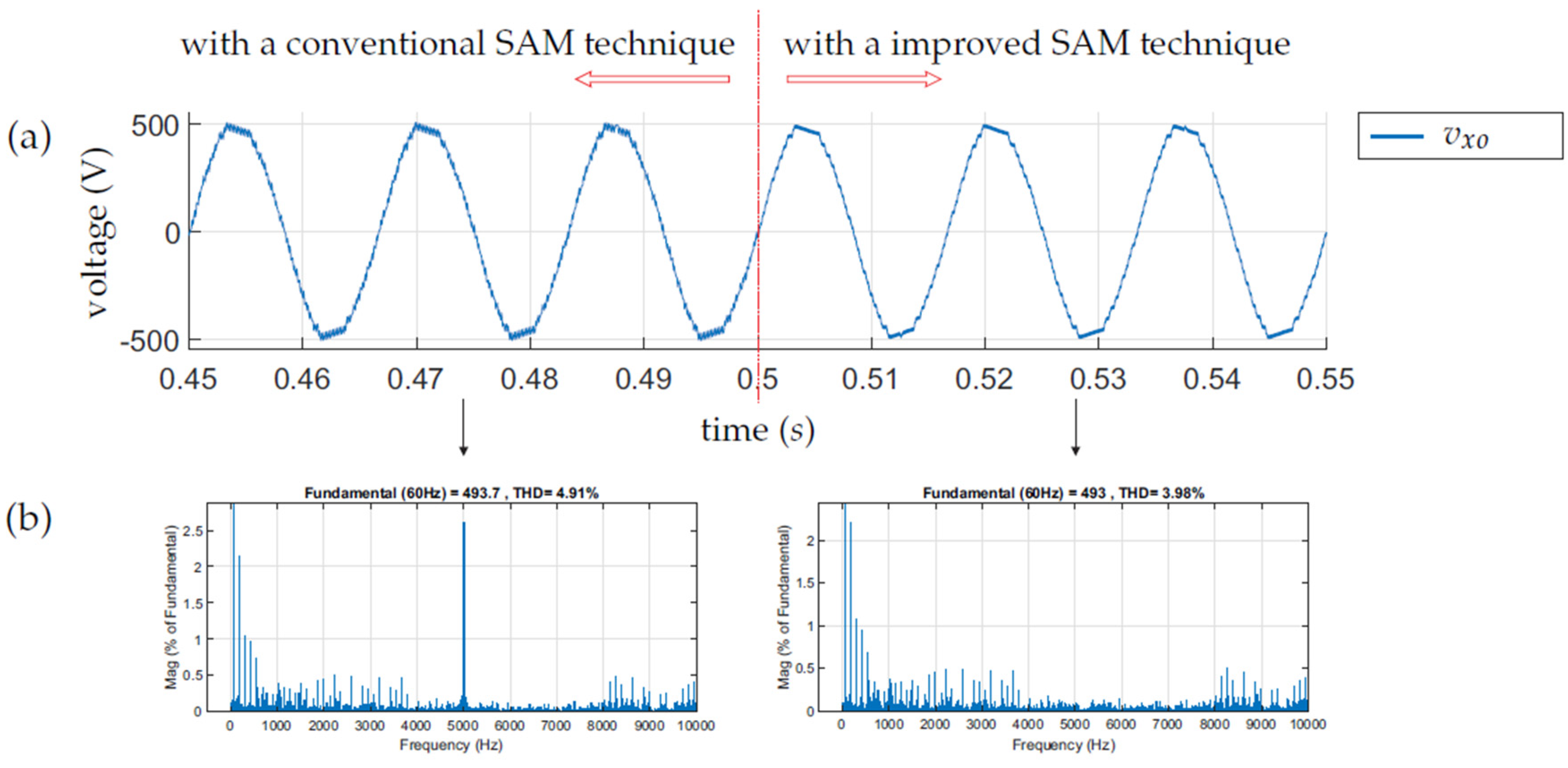
- The THD of the inverter output voltage (line-to-ground), [THD (%)], it is probably the most important parameter when considering a suitable modulation technique, due to this parameter defines the inherent passive components sizing (submodule capacitor and arm inductor) and external components to the MMC (line filters, rated power devices, according to the application).
- (2)
- The output voltage fundamental value, [ (V)], it is observed to check if the technique used ensures an adequate value without compromising the effectiveness of the MMC, this parameter is important for MMC with reduced number of submodules, which usually tends to be a problem as in Staircase modulation technique, this issue is widely discussed in [33].
- (3)
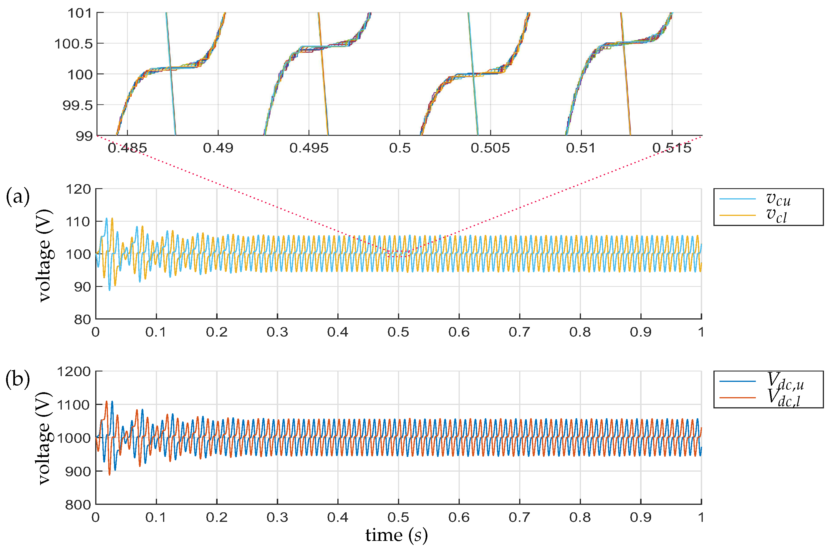
- The peak-to-peak variation of the capacitor voltage of upper and lower arm submodules, [ (V)], this parameter characterizes the suitable capacitor sizing and for that, firstly, it is necessary to define the modulation technique and then a suitable sizing method is applied for the inherent components. Since, the capacitor and the inductor inherent to the MMC should be sized relative to a modulation technique, so that, the dynamic behavior of the converter will be adequate for that specific method. In this case, standard sizing methods studied in Section 2 are used and, when compared to other modulation techniques, it was obtained an acceptable performance.
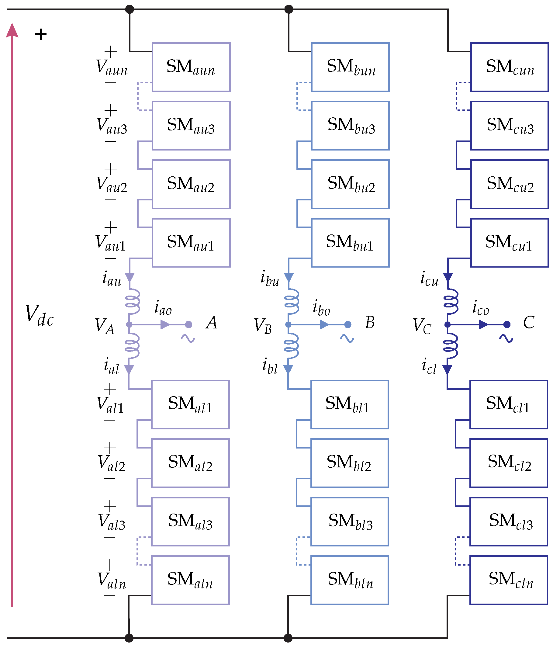
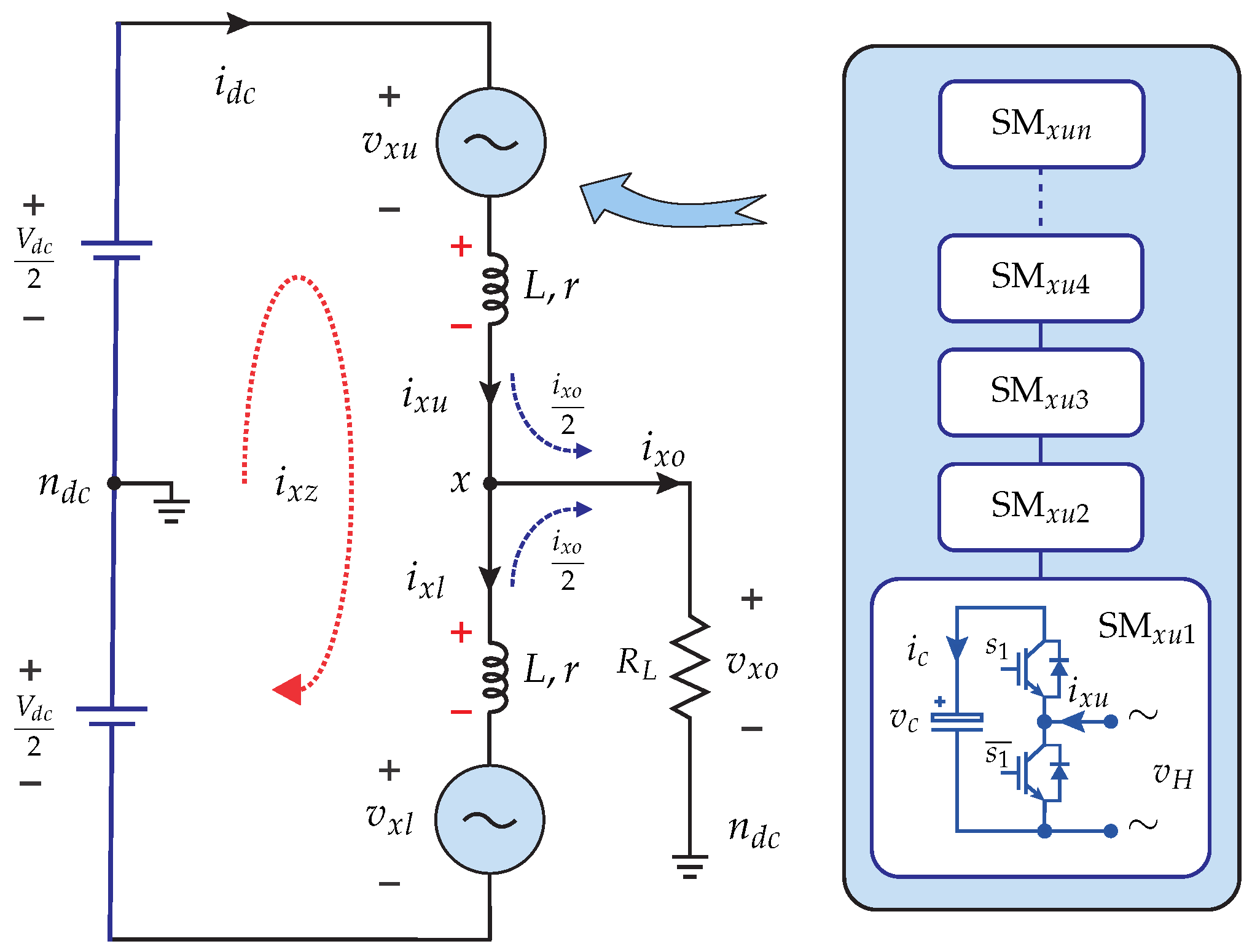
2. The MMC Operating Principles
2.1. Basic Principles
2.2. Mathematical Model
2.3. AC Circulating Current
2.4. Submodule Capacitor Sizing
2.5. Arm Inductor Sizing
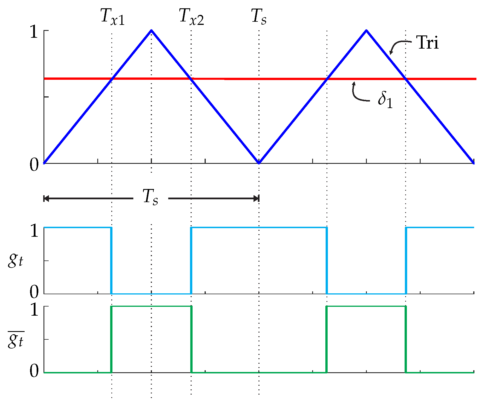
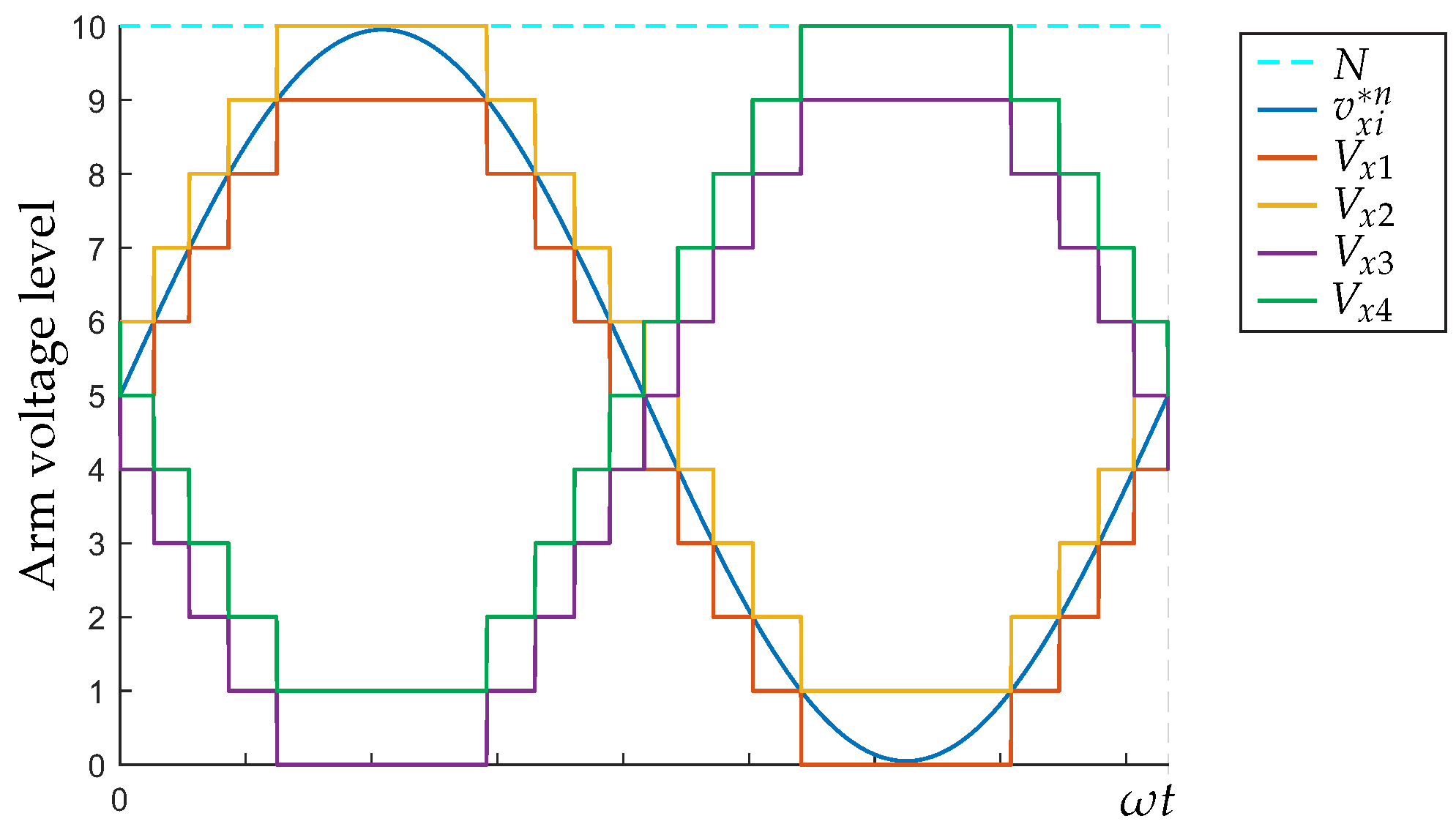
3. Conventional SAM Technique
3.1. Identification of Two Nearest Voltages
3.2. Calculation of Dwell Times
3.3. Calculation of the Arm Voltage Levels
- ∘
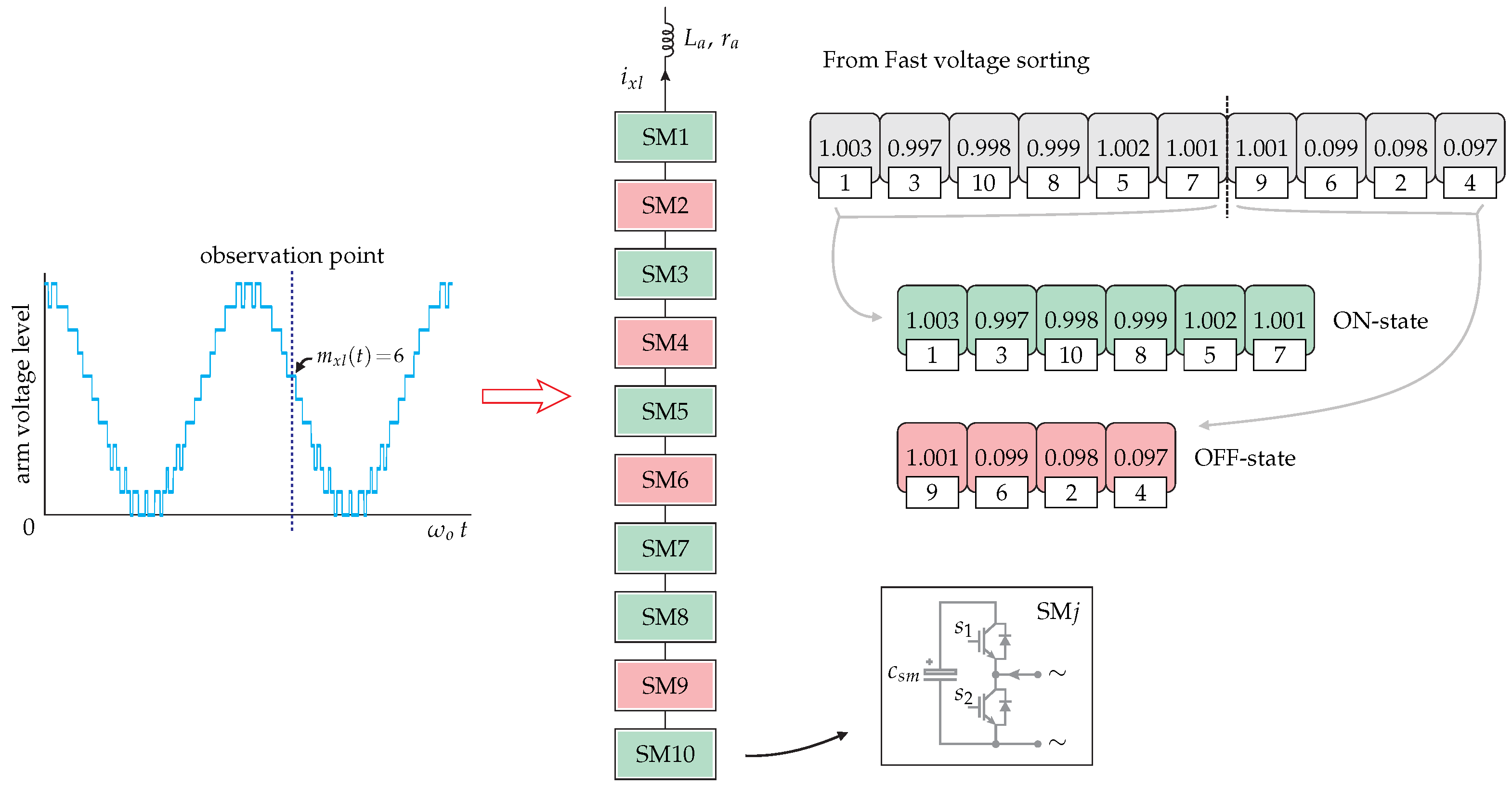
- In each sampling period, the number of submodules in ON-satate, considering the upper and lower arm, is maintained constant and equal to N (remember that the total number of submodules in one leg is equal to ).
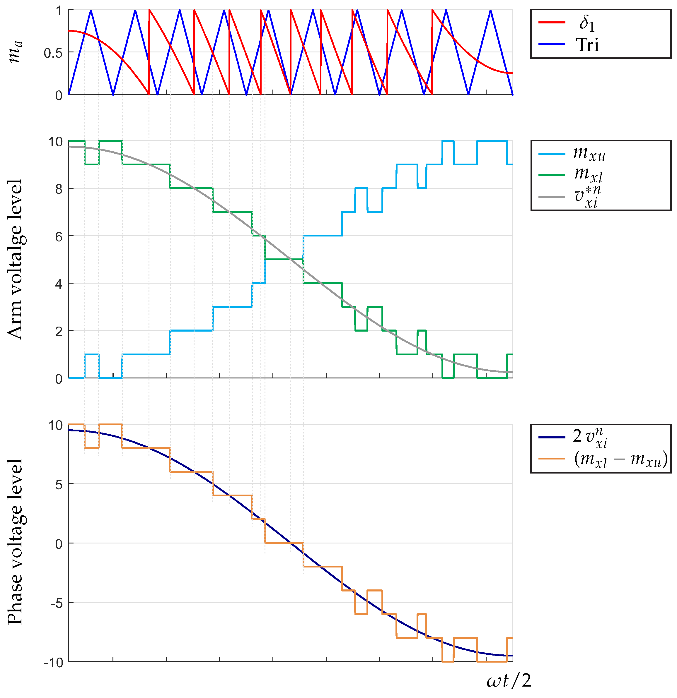
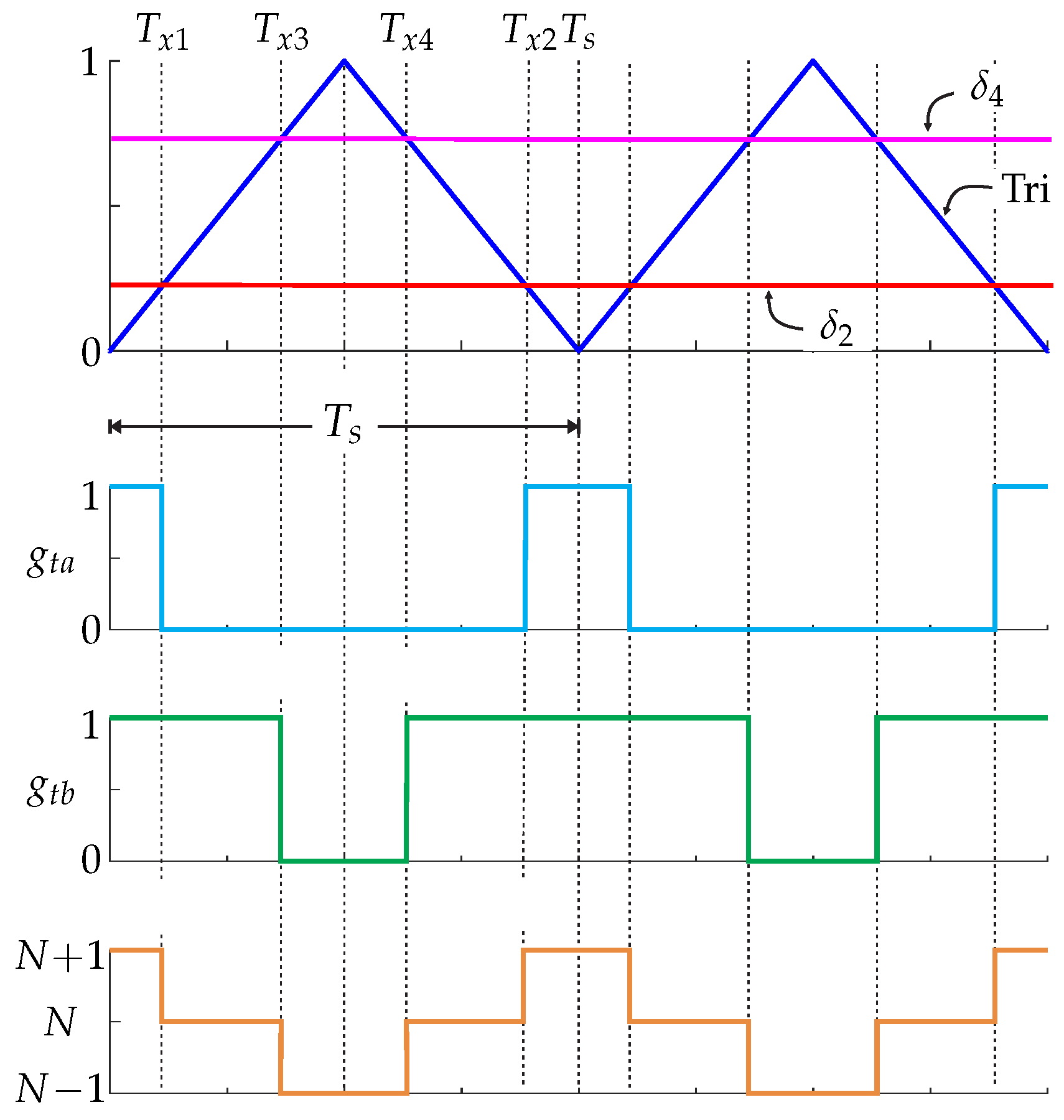
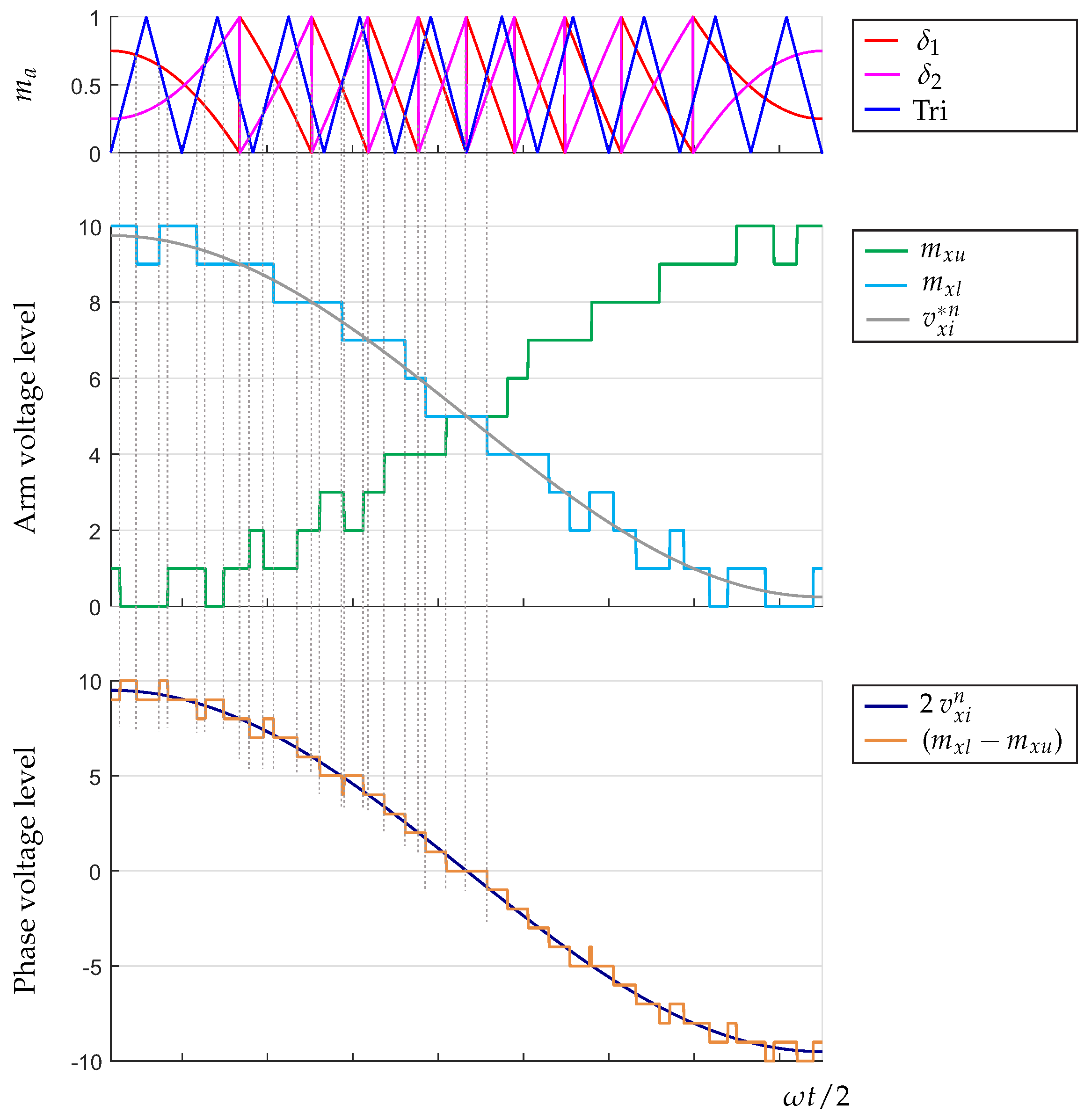
4. Improved SAM Technique
- The phase voltage waveform has levels only.
- The high THD’s value of the inverter output voltage.
4.1. Identification of Two Nearest Voltages
4.2. Calculation of Dwell Times
4.3. Calculation of Arm Voltage Levels
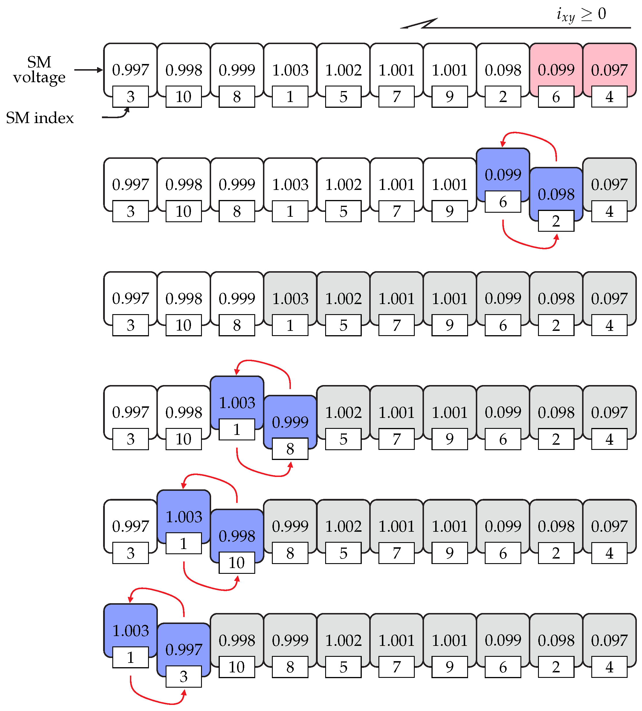
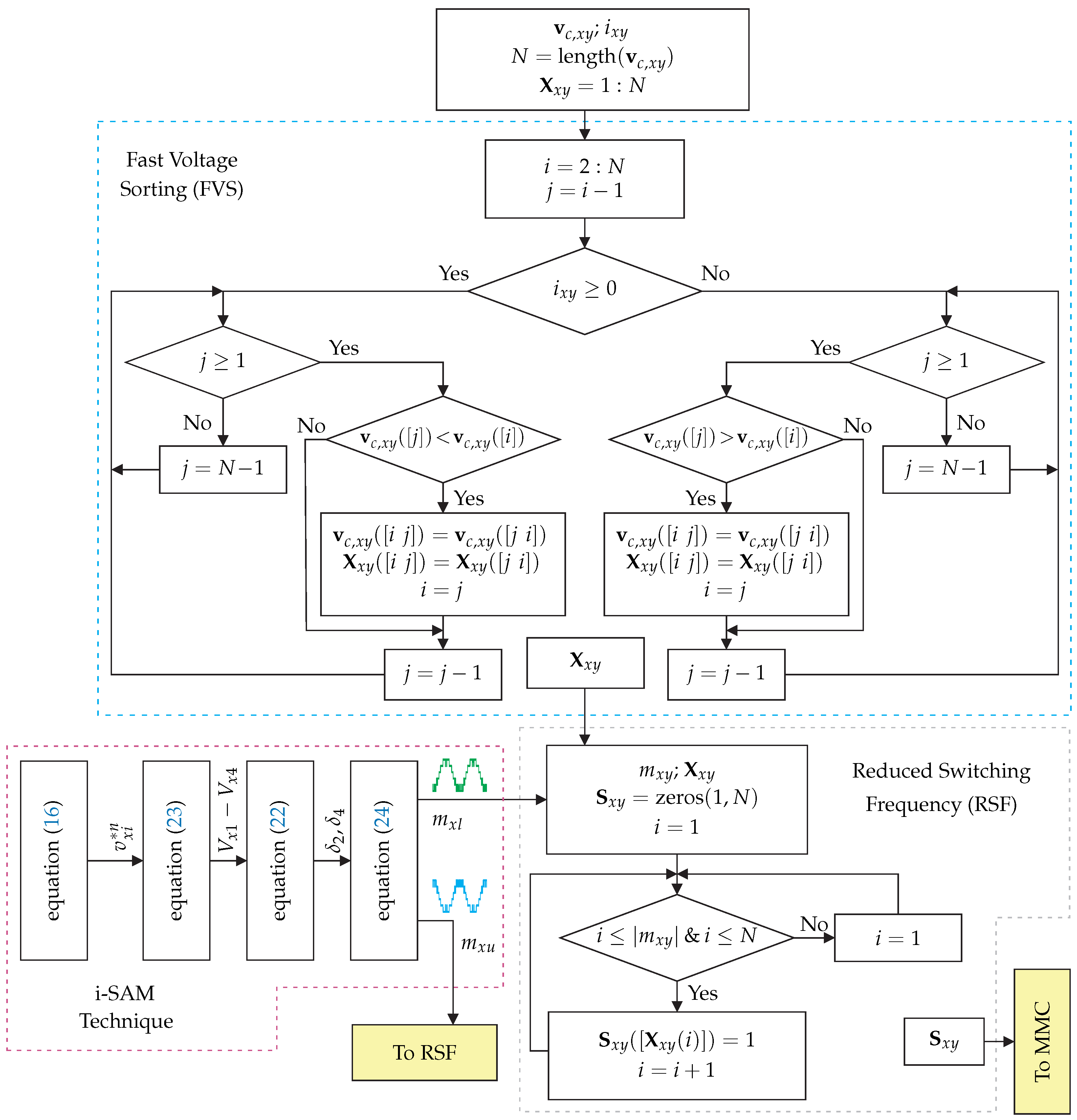
5. Voltage Balancing Algorithm Proposed
5.1. Fast Voltage Sorting Algorithm
5.2. Reduced Switching Frequency
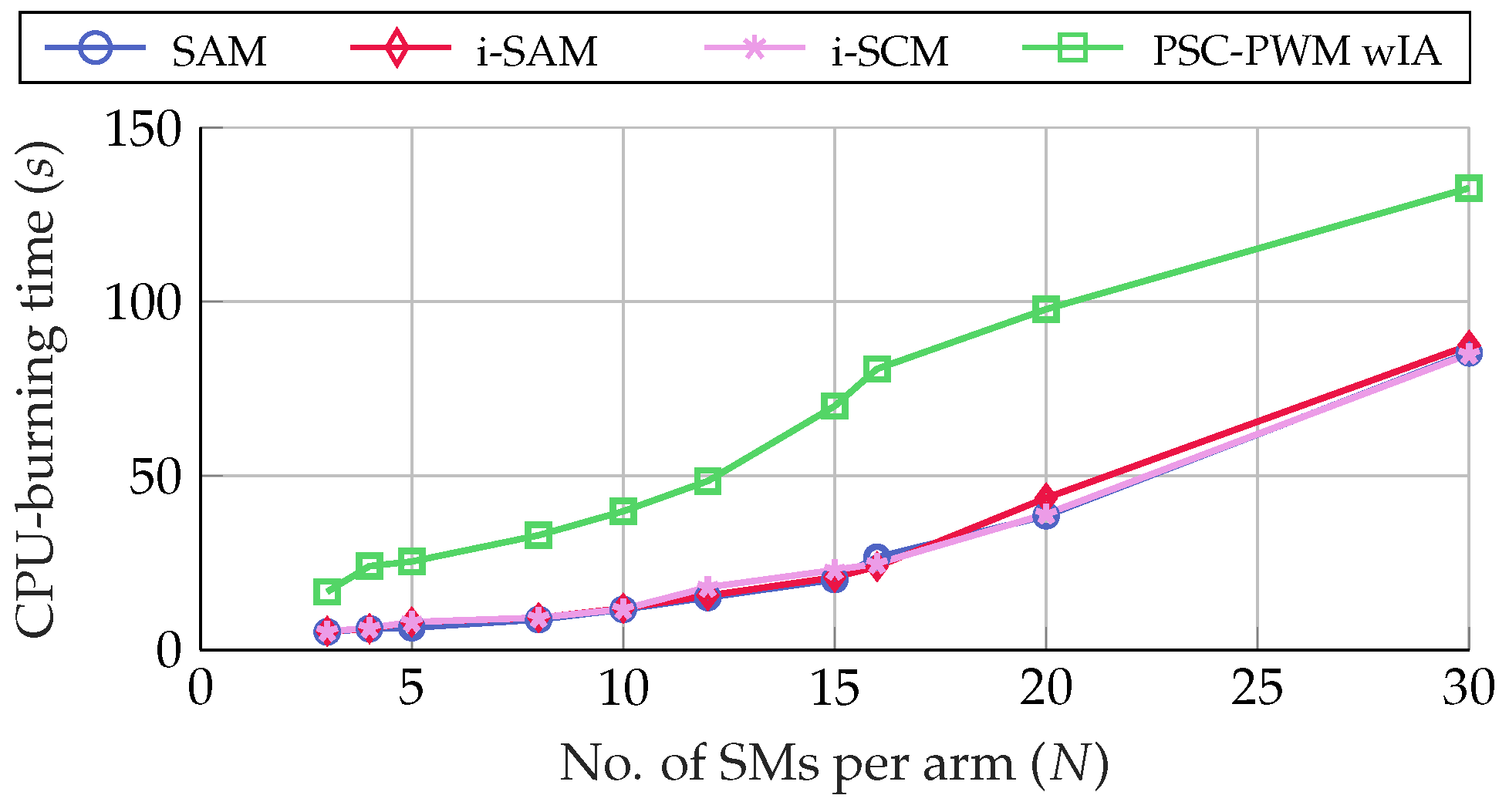
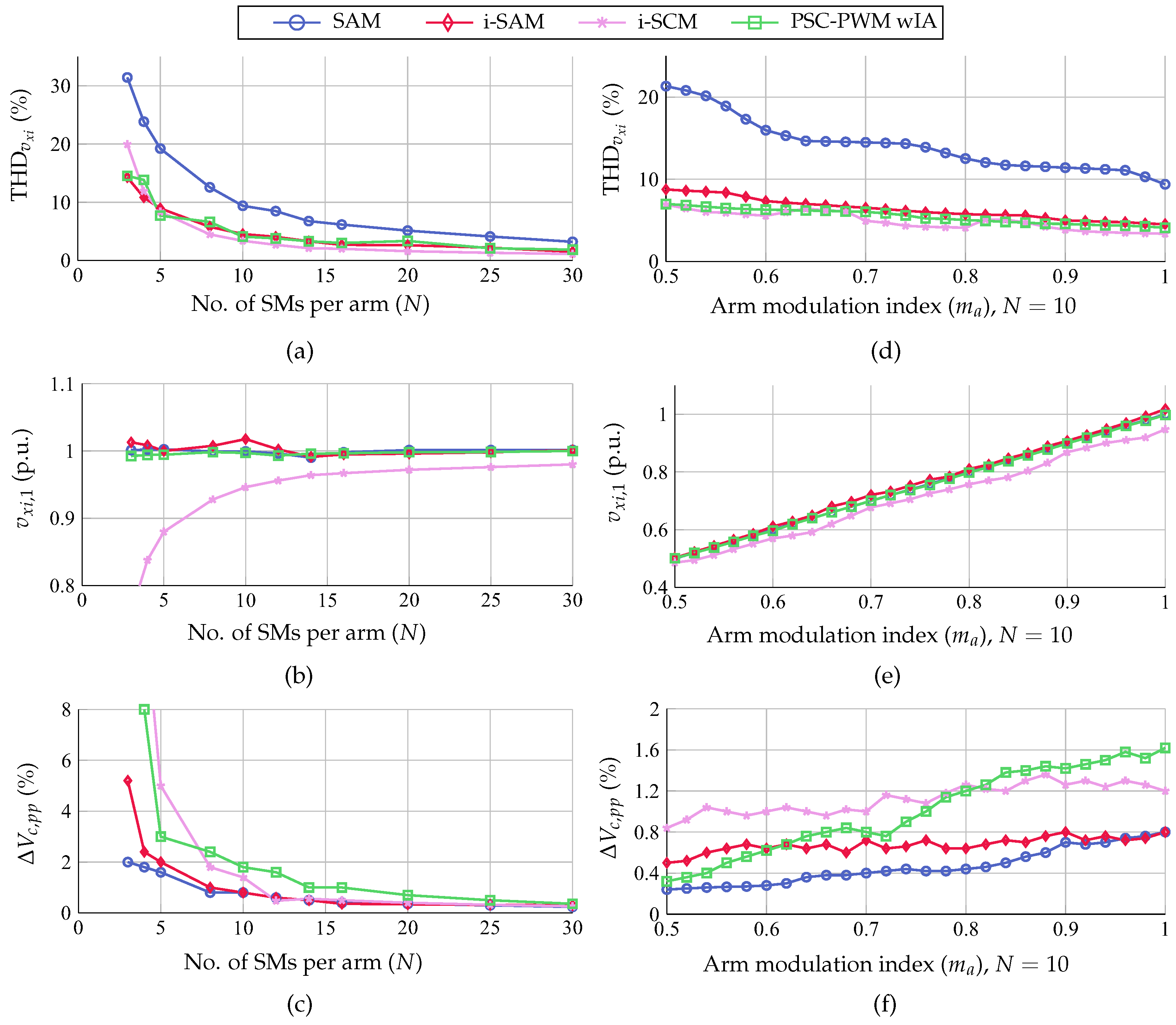
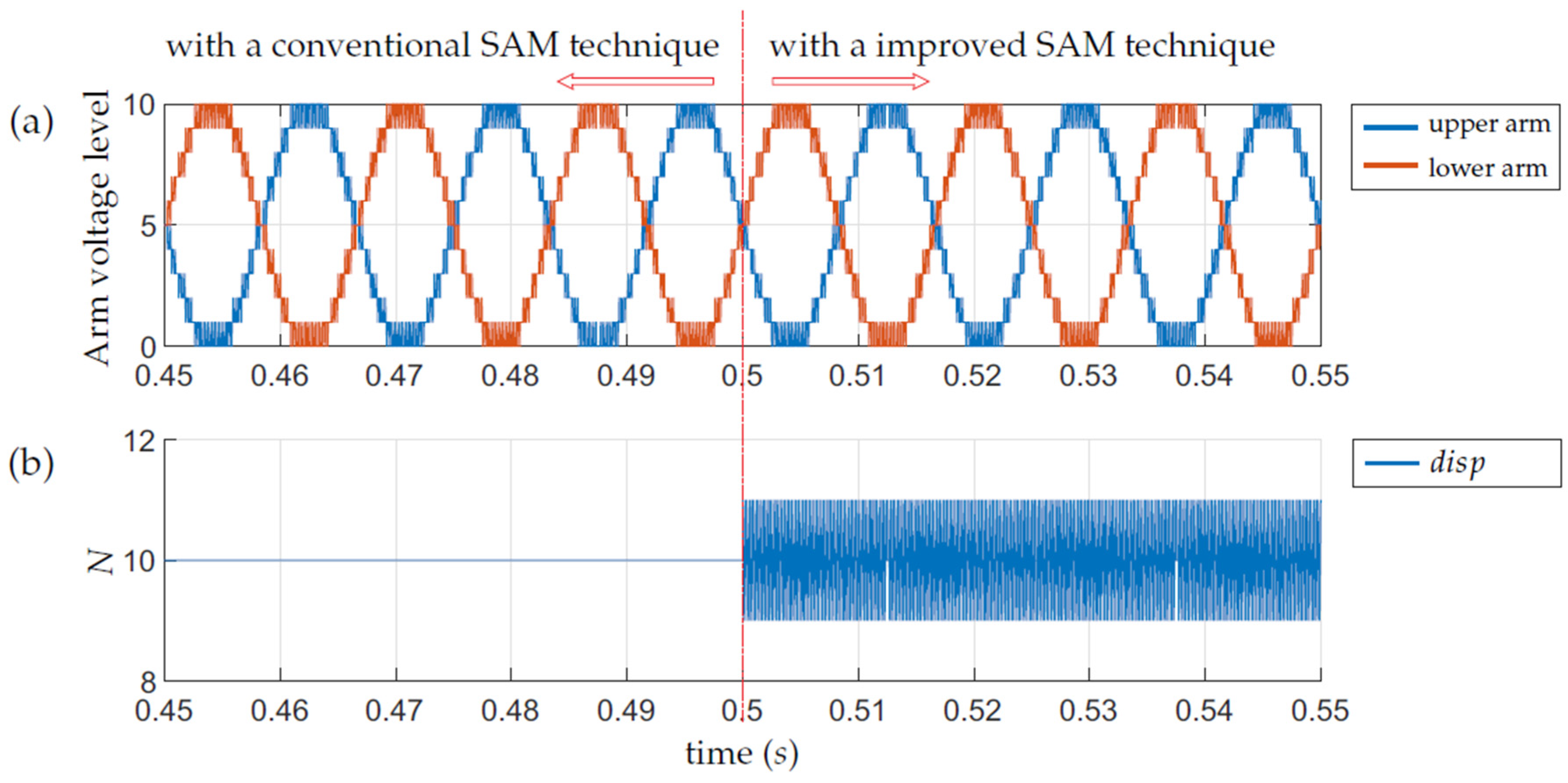
6. Simulation Results
- (1)
- The THD of the inverter output voltage (line-to-ground), [THD (%)], it is probably the most important parameter when considering a suitable modulation technique, due to this parameter defines the inherent passive components sizing (submodule capacitor and arm inductor) and external components to the MMC (line filters, rated power devices, according to the application).
- (2)
- The output voltage fundamental value, [ (p.u.)], it is observed to check if the technique used ensures an adequate value without compromising the effectiveness of the MMC, this parameter is important for MMC with reduced number of submodules, which usually tends to be a problem as in Staircase modulation technique, this issue is widely discussed in [33].
- (3)
- The peak-to-peak variation of the capacitor voltage of upper and lower arm submodules, [ (%)], this parameter characterizes the suitable capacitor sizing and for that, firstly, it is necessary to define the modulation technique and then a suitable sizing method is applied for the inherent components. Since, the capacitor and the inductor inherent to the MMC should be sized relative to a modulation technique, so that, the dynamic behavior of the converter will be adequate for that specific method. In this case, standard sizing methods studied in Section 2 are used and, when compared to other modulation techniques, it was obtained an acceptable performance.
Case of Study: Single-Phase
7. Conclusions
Author Contributions
Funding
Institutional Review Board Statement
Informed Consent Statement
Data Availability Statement
Acknowledgments
Conflicts of Interest
Abbreviations
| VSC | Voltage Source Converter |
| MLC | Multilevel Converter |
| MMC | Modular Multilevel Converter |
| PWM | Pulse Width Modulation |
References
- Gupta, K.K.; Ranjan, A.; Bhatnagar, P.; Sahu, L.K.; Jain, S. Multilevel Inverter Topologies With Reduced Device Count: A Review. IEEE Trans. Power Electron. 2016, 31, 135–151. [Google Scholar] [CrossRef]
- Priya, M.; Ponnambalam, P.; Muralikumar, K. Modular-multilevel converter topologies and applications—A review. IET Power Electron. 2018, 12, 170–183. [Google Scholar] [CrossRef]
- Vijeh, M.; Rezanejad, M.; Samadaei, E.; Bertilsson, K. A general review of multilevel inverters based on main submodules: Structural point of view. IEEE Trans. Power Electron. 2019, 34, 9479–9502. [Google Scholar] [CrossRef]
- Marquardt, R.; Lesnicar, A.; Hildinger, J. Modulares Stromrichterkonzept für Netzkupplungsanwendung bei Hohen Spannungen; ETG-Fachtagung: Bad Nauheim, Germany, 2002; Volume 114. [Google Scholar]
- Du, S.; Dekka, A.; Wu, B.; Zargari, N. Modular Multilevel Converters: Analysis, Control, and Applications; John Wiley & Sons: Hoboken, NJ, USA, 2018. [Google Scholar]
- Perez, M.A.; Bernet, S.; Rodriguez, J.; Kouro, S.; Lizana, R. Circuit topologies, modeling, control schemes, and applications of modular multilevel converters. IEEE Trans. Power Electron. 2014, 30, 4–17. [Google Scholar] [CrossRef]
- Debnath, S.; Qin, J.; Bahrani, B.; Saeedifard, M.; Barbosa, P. Operation, control, and applications of the modular multilevel converter: A review. IEEE Trans. Power Electron. 2014, 30, 37–53. [Google Scholar] [CrossRef]
- Shu, Z.; Liu, M.; Zhao, L.; Song, S.; Zhou, Q.; He, X. Predictive harmonic control and its optimal digital implementation for MMC-based active power filter. IEEE Trans. Ind. Electron. 2016, 63, 5244–5254. [Google Scholar] [CrossRef]
- Antonopoulos, A.; Ängquist, L.; Norrga, S.; Ilves, K.; Harnefors, L.; Nee, H.P. Modular multilevel converter ac motor drives with constant torque from zero to nominal speed. IEEE Trans. Ind. Appl. 2013, 50, 1982–1993. [Google Scholar] [CrossRef]
- Li, B.; Zhou, S.; Xu, D.; Finney, S.J.; Williams, B.W. A hybrid modular multilevel converter for medium-voltage variable-speed motor drives. IEEE Trans. Power Electron. 2016, 32, 4619–4630. [Google Scholar] [CrossRef] [Green Version]
- Nademi, H.; Das, A.; Burgos, R.; Norum, L.E. A new circuit performance of modular multilevel inverter suitable for photovoltaic conversion plants. IEEE J. Emerg. Sel. Top. Power Electron. 2015, 4, 393–404. [Google Scholar] [CrossRef]
- Rong, F.; Gong, X.; Huang, S. A novel grid-connected PV system based on MMC to get the maximum power under partial shading conditions. IEEE Trans. Power Electron. 2016, 32, 4320–4333. [Google Scholar] [CrossRef]
- Steurer, M.M.; Schoder, K.; Faruque, O.; Soto, D.; Bosworth, M.; Sloderbeck, M.; Bogdan, F.; Hauer, J.; Winkelnkemper, M.; Schwager, L.; et al. Multifunctional megawatt-scale medium voltage DC test bed based on modular multilevel converter technology. IEEE Trans. Transp. Electrif. 2016, 2, 597–606. [Google Scholar] [CrossRef]
- Raza, M.; Prieto-Araujo, E.; Gomis-Bellmunt, O. Small-signal stability analysis of offshore AC network having multiple VSC-HVDC systems. IEEE Trans. Power Deliv. 2017, 33, 830–839. [Google Scholar] [CrossRef]
- Xu, Q.; Ma, F.; He, Z.; Chen, Y.; Guerrero, J.M.; Luo, A.; Li, Y.; Yue, Y. Analysis and comparison of modular railway power conditioner for high-speed railway traction system. IEEE Trans. Power Electron. 2016, 32, 6031–6048. [Google Scholar] [CrossRef] [Green Version]
- Ronanki, D.; Williamson, S.S. Modular multilevel converters for transportation electrification: Challenges and opportunities. IEEE Trans. Transp. Electrif. 2018, 4, 399–407. [Google Scholar] [CrossRef]
- Chen, Y.; Li, Z.; Zhao, S.; Wei, X.; Kang, Y. Design and implementation of a modular multilevel converter with hierarchical redundancy ability for electric ship MVDC system. IEEE J. Emerg. Sel. Top. Power Electron. 2016, 5, 189–202. [Google Scholar] [CrossRef]
- Chen, Y.; Zhao, S.; Li, Z.; Wei, X.; Kang, Y. Modeling and control of the isolated DC–DC modular multilevel converter for electric ship medium voltage direct current power system. IEEE J. Emerg. Sel. Top. Power Electron. 2016, 5, 124–139. [Google Scholar] [CrossRef]
- Li, B.; Shi, S.; Xu, D.; Wang, W. Control and analysis of the modular multilevel DC de-icer with statcom functionality. IEEE Trans. Ind. Electron. 2016, 63, 5465–5476. [Google Scholar] [CrossRef]
- Nguyen, T.H.; Al Hosani, K.; El Moursi, M.S.; Blaabjerg, F. An overview of modular multilevel converters in HVDC transmission systems with STATCOM operation during pole-to-pole DC short circuits. IEEE Trans. Power Electron. 2018, 34, 4137–4160. [Google Scholar] [CrossRef]
- Lesnicar, A.; Marquardt, R. An innovative modular multilevel converter topology suitable for a wide power range. In Proceedings of the 2003 IEEE Bologna Power Tech Conference Proceedings, Bologna, Italy, 23–26 June 2003; Volume 3. [Google Scholar]
- Deng, F.; Zhu, R.; Liu, D.; Wang, Y.; Wang, H.; Chen, Z.; Cheng, M. Protection scheme for modular multilevel converters under diode open-circuit faults. IEEE Trans. Power Electron. 2017, 33, 2866–2877. [Google Scholar] [CrossRef] [Green Version]
- Luo, Y.; Li, Z.; Xu, L.; Xiong, X.; Li, Y.; Zhao, C. An adaptive voltage-balancing method for high-power modular multilevel converters. IEEE Trans. Power Electron. 2017, 33, 2901–2912. [Google Scholar] [CrossRef]
- Dekka, A.; Wu, B.; Yaramasu, V.; Zargari, N.R. Model predictive control with common-mode voltage injection for modular multilevel converter. IEEE Trans. Power Electron. 2016, 32, 1767–1778. [Google Scholar] [CrossRef]
- Dekka, A.; Wu, B.; Fuentes, R.L.; Perez, M.; Zargari, N.R. Evolution of topologies, modeling, control schemes, and applications of modular multilevel converters. IEEE J. Emerg. Sel. Top. Power Electron. 2017, 5, 1631–1656. [Google Scholar] [CrossRef]
- Dekka, A.; Wu, B.; Yaramasu, V.; Fuentes, R.L.; Zargari, N.R. Model Predictive Control of High-Power Modular Multilevel Converters—An Overview. IEEE J. Emerg. Sel. Top. Power Electron. 2018, 7, 168–183. [Google Scholar] [CrossRef]
- Wang, J.; Burgos, R.; Boroyevich, D. Switching-cycle state-space modeling and control of the modular multilevel converter. IEEE J. Emerg. Sel. Top. Power Electron. 2014, 2, 1159–1170. [Google Scholar] [CrossRef]
- Li, J.; Konstantinou, G.; Wickramasinghe, H.R.; Pou, J.; Wu, X.; Jin, X. Investigation of MMC-HVDC operating region by circulating current control under grid imbalances. Electr. Power Syst. Res. 2017, 152, 211–222. [Google Scholar] [CrossRef]
- Dekka, A.; Wu, B.; Zargari, N.R. A novel modulation scheme and voltage balancing algorithm for modular multilevel converter. IEEE Trans. Ind. Appl. 2016, 52, 432–443. [Google Scholar] [CrossRef]
- Konstantinou, G.S.; Agelidis, V.G. Performance evaluation of half-bridge cascaded multilevel converters operated with multicarrier sinusoidal PWM techniques. In Proceedings of the 2009 4th IEEE Conference on Industrial Electronics and Applications, Xi’an, China, 25–27 May 2009; pp. 3399–3404. [Google Scholar]
- Wang, K.; Zhou, L.; Deng, Y.; Lu, Y.; Wang, C.; Xu, F. Application range analysis and implementation of the logic-processed CPS-PWM scheme based mmc capacitor voltage balancing strategy. CPSS Trans. Power Electron. Appl. 2019, 4, 1–9. [Google Scholar] [CrossRef]
- Hu, P.; Jiang, D. A level-increased nearest level modulation method for modular multilevel converters. IEEE Trans. Power Electron. 2014, 30, 1836–1842. [Google Scholar] [CrossRef]
- Lin, L.; Lin, Y.; He, Z.; Chen, Y.; Hu, J.; Li, W. Improved nearest-level modulation for a modular multilevel converter with a lower submodule number. IEEE Trans. Power Electron. 2016, 31, 5369–5377. [Google Scholar] [CrossRef]
- Colque, J.C.; Ruppert, E.; Vargas, R.Z.; Azcue, J.L. Comparative analysis based on the switching frequency of modulation techniques for MMC applications. In Proceedings of the 2019 IEEE 15th Brazilian Power Electronics Conference and 5th IEEE Southern Power Electronics Conference (COBEP/SPEC), Santos, Brazil, 1–4 December 2019; pp. 1–6. [Google Scholar]
- Meshram, P.M.; Borghate, V.B. A simplified nearest level control (NLC) voltage balancing method for modular multilevel converter (MMC). IEEE Trans. Power Electron. 2014, 30, 450–462. [Google Scholar] [CrossRef]
- Far, Z.D.; Radan, A.; Far, M.D. Introduction and evaluation of novel multi-level carrier-based PWM strategies using a generalized algorithm. In Proceedings of the 2007 European Conference on Power Electronics and Applications, Aalborg, Denmark, 2–5 September 2007; pp. 1–10. [Google Scholar]
- Wang, H.; Zhao, R.; Deng, Y.; He, X. Novel carrier-based PWM methods for multilevel inverter. In Proceedings of the IECON’03. 29th Annual Conference of the IEEE Industrial Electronics Society (IEEE Cat. No. 03CH37468), Roanoke, VA, USA, 2–6 November 2003; Volume 3, pp. 2777–2782. [Google Scholar]
- Konstantinou, G.; Darus, R.; Pou, J.; Ceballos, S.; Agelidis, V.G. Varying and unequal carrier frequency PWM techniques for modular multilevel converters. In Proceedings of the 2014 International Power Electronics Conference (IPEC-Hiroshima 2014-ECCE ASIA), Hiroshima, Japan, 18–21 May 2014; pp. 3758–3763. [Google Scholar]
- Konstantinou, G.; Ciobotaru, M.; Agelidis, V. Selective harmonic elimination pulse-width modulation of modular multilevel converters. IET Power Electron. 2013, 6, 96–107. [Google Scholar] [CrossRef]
- Pérez-Basante, A.; Ceballos, S.; Konstantinou, G.; Pou, J.; Andreu, J.; de Alegría, I.M. (2N + 1) Selective harmonic elimination-PWM for modular multilevel converters: A generalized formulation and a circulating current control method. IEEE Trans. Power Electron. 2017, 33, 802–818. [Google Scholar] [CrossRef]
- Dahidah, M.S.; Konstantinou, G.; Agelidis, V.G. A review of multilevel selective harmonic elimination PWM: Formulations, solving algorithms, implementation and applications. IEEE Trans. Power Electron. 2014, 30, 4091–4106. [Google Scholar] [CrossRef]
- Li, B.; Yang, R.; Xu, D.; Wang, G.; Wang, W.; Xu, D. Analysis of the phase-shifted carrier modulation for modular multilevel converters. IEEE Trans. Power Electron. 2014, 30, 297–310. [Google Scholar] [CrossRef]
- Deng, Y.; Wang, Y.; Teo, K.H.; Harley, R.G. A simplified space vector modulation scheme for multilevel converters. IEEE Trans. Power Electron. 2015, 31, 1873–1886. [Google Scholar] [CrossRef]
- Dekka, A.; Wu, B.; Zargari, N.R.; Fuentes, R.L. A space-vector PWM-based voltage-balancing approach with reduced current sensors for modular multilevel converter. IEEE Trans. Ind. Electron. 2016, 63, 2734–2745. [Google Scholar] [CrossRef]
- Colque, J.C.; Ruppert, E.; Delgado-Hayta, I.; Azcue, J.L. A new space-vector selector modulation for the modular multilevel converter applications. In Proceedings of the 2020 IEEE XXVII International Conference on Electronics, Electrical Engineering and Computing (INTERCON), Lima, Peru, 3–5 September 2020; pp. 1–4. [Google Scholar]
- Rohner, S.; Bernet, S.; Hiller, M.; Sommer, R. Modulation, losses, and semiconductor requirements of modular multilevel converters. IEEE Trans. Ind. Electron. 2009, 57, 2633–2642. [Google Scholar] [CrossRef]
- Li, Z.; Wang, P.; Zhu, H.; Chu, Z.; Li, Y. An improved pulse width modulation method for chopper-cell-based modular multilevel converters. IEEE Trans. Power Electron. 2012, 27, 3472–3481. [Google Scholar] [CrossRef]
- Edpuganti, A.; Rathore, A.K. Optimal pulsewidth modulation of medium-voltage modular multilevel converter. IEEE Trans. Ind. Appl. 2016, 52, 3435–3442. [Google Scholar] [CrossRef]
- Gong, Z.; Wu, X.; Dai, P.; Zhu, R. Modulated model predictive control for MMC-based active front-end rectifiers under unbalanced grid conditions. IEEE Trans. Ind. Electron. 2018, 66, 2398–2409. [Google Scholar] [CrossRef]
- Gupta, R.; Ghosh, A.; Joshi, A. Multiband hysteresis modulation and switching characterization for sliding-mode-controlled cascaded multilevel inverter. IEEE Trans. Ind. Electron. 2009, 57, 2344–2353. [Google Scholar] [CrossRef]
- Marquardt, R.; Lesnicar, A. A new modular voltage source inverter topology. In Proceedings of the Euro Conference of Power Electronics Applications, Toulouse, France, 2–4 September 2003; pp. 1–6. [Google Scholar]
- Tu, Q.; Xu, Z.; Huang, H.; Zhang, J. Parameter design principle of the arm inductor in modular multilevel converter based HVDC. In Proceedings of the 2010 International Conference on Power System Technology, Hangzhou, China, 24–28 October 2010; pp. 1–6. [Google Scholar]
- Vatani, M.; Bahrani, B.; Saeedifard, M.; Hovd, M. Indirect finite control set model predictive control of modular multilevel converters. IEEE Trans. Smart Grid 2014, 6, 1520–1529. [Google Scholar] [CrossRef] [Green Version]


| Family | Techniques | Refs. | Dynamic Response | Implementation Complexity | Inverter Output Waveform Levels | Switching Frequency |
|---|---|---|---|---|---|---|
| Nearest Voltage Level | SCM | [35] | fast | low | fund. | |
| i-SCM | [32,33] | fast | low | fund. | ||
| Level Shifted Carrier | PD-PWM | [30,36] | moderate | medium | high | |
| POD-PWM | [30,36] | moderate | medium | high | ||
| APOD-PWM | [30,36] | moderate | medium | high | ||
| VF-PWM | [37,38] | moderate | medium | high | ||
| VFb-PWM | [38] | moderate | medium | high | ||
| Reprogrammed PWM | SHE | [39] | fast | medium | fund. | |
| i-SHE | [40] | fast | medium | fund. | ||
| SHM | [41] | fast | medium | fund. | ||
| Sub-harmonics | PSC-PWM | [30,31] | moderate | medium | med.–high | |
| PSC-PWM wIA | [31,42] | slow | medium | high | ||
| SD-PWM | [30] | moderate | medium | med.–high | ||
| HPS-PWM | [37] | moderate | medium | high | ||
| Space Vector | SV-PWM | [43] | slow | medium | low | |
| dual SV-PWM | [44] | slow | high | low | ||
| vector selector | [45] | slow | medium | fund.–var. | ||
| Submodules Unified | SU-PWM | [46] | moderate | medium | low | |
| i-SU-PWM | [47] | moderate | medium | low | ||
| Sampled Average Mod. | SAM | [29] | fast | medium | low–med. | |
| improved SAM | fast | medium | low–med | |||
| CO-PWM | [36] | moderate | medium | med.–high | ||
| SO-PMW | [48] | moderate | medium | fund./low | ||
| Modulated MPC-PWM | [49] | fast | high | variable | ||
| Multiband Hysteresis Modulation | [50] | moderate | medium | variable | ||
| Item | Variable | Value | Unit |
|---|---|---|---|
| Rated apparent power | S | 8000 | VA |
| DC-link voltage | 1000 | V | |
| Inverter output frequency | 60 | Hz | |
| Switching frequency | 1200 | Hz | |
| Load resistance | 125 | Ω | |
| Power factor | PF | 0.95 | |
| Arm modulation index | 0.99 | ||
| Sample time | 50 μs | ||
| Simulink solver | ode23t (mod. stiff/Trapezoidal) | ||
| Processor AMD A8-5500B APU | 3.20 | GHz | |
| No. of SMs/arm | (mF) | No. of SMs/arm | (mF) |
|---|---|---|---|
| 3 | 0.62 | 12 | 2.25 |
| 4 | 0.84 | 15 | 3.12 |
| 5 | 1.01 | 16 | 3.32 |
| 8 | 1.74 | 20 | 4.15 |
| 10 | 2.18 | 30 | 6.24 |
| 120 | 25.4 |
Publisher’s Note: MDPI stays neutral with regard to jurisdictional claims in published maps and institutional affiliations. |
© 2022 by the authors. Licensee MDPI, Basel, Switzerland. This article is an open access article distributed under the terms and conditions of the Creative Commons Attribution (CC BY) license (https://creativecommons.org/licenses/by/4.0/).
Share and Cite
Colque, J.C.; Filho, E.R.; Azcue, J.L. Improved Sampled Average Modulation Technique for the Modular Multilevel Converters. Energies 2022, 15, 4554. https://doi.org/10.3390/en15134554
Colque JC, Filho ER, Azcue JL. Improved Sampled Average Modulation Technique for the Modular Multilevel Converters. Energies. 2022; 15(13):4554. https://doi.org/10.3390/en15134554
Chicago/Turabian StyleColque, Juan Carlos, Ernesto Ruppert Filho, and José Luis Azcue. 2022. "Improved Sampled Average Modulation Technique for the Modular Multilevel Converters" Energies 15, no. 13: 4554. https://doi.org/10.3390/en15134554
APA StyleColque, J. C., Filho, E. R., & Azcue, J. L. (2022). Improved Sampled Average Modulation Technique for the Modular Multilevel Converters. Energies, 15(13), 4554. https://doi.org/10.3390/en15134554