Article

A Trans-Inverse Magnetic Coupling Single-Phase AC-AC Converter

1
Department of Electrical Engineering, Mazandaran University of Science and Technology, Babol 47166-85635, Iran
2
Department of Electrical Engineering, Amirkabir University of Technology, Tehran 15916-34311, Iran
3
Department of Electrical Engineering, Technical and Vocational University (TVU), Tehran 14357-61137, Iran
4
Faculty of Engineering and Applied Science, Memorial University of Newfoundland, St. John’s, NL A1B 3X5, Canada
5
College of Science and Engineering, Flinders University, Adelaide 5042, Australia
*
Author to whom correspondence should be addressed.
Energies 2022, 15(12), 4319; https://doi.org/10.3390/en15124319
Submission received: 10 April 2022 / Revised: 31 May 2022 / Accepted: 8 June 2022 / Published: 13 June 2022

Abstract

:
This paper introduces a new single-phase AC-AC converter based on an impedance source circuit. Like the existing single-phase impedance source AC-AC converters, it has the buck-boost ability and direct ac conversion. The input and output voltage possesses the same ground, and the phase angle is maintained and reversed smoothly. The presented converter utilizes a coupled transformer which allows the designer to exploit the transformer’s turns ratio as a variable to attain the desired output voltage. Additionally, the used transformer provides an option to obtain higher voltage gain by decreasing the turns ratio. Hence, smaller size of the coupled inductors is required for the higher voltage cases. To eliminate the switching voltage and current spikes on the power switches, a safe commutation strategy is used instead of utilizing snubber circuits. Furthermore, the input current is continuous and sinusoidal with low harmonics thanks to embedding the input inductor in series with the input source. Additionally, a dynamic voltage restorer is presented based on the proposed converter to compensate the voltage sag and swell faults. Simulation results are provided to evaluate the theoretical analysis. Finally, a laboratory prototype has been fabricated to demonstrate the validation of the presented converter.

1. Introduction

Nowadays, power quality problems are among the most critical concerns for sensitive loads’ consumers. Voltage sags and swells are the most common power quality issues, especially for single-phase home appliances. Recently, single-phase AC-AC converters have been exploited widely among sensitive loads to compensate voltage sags and swells [1]. Conventional indirect AC-AC converters, including two AC-DC and dc-ac conversions, have to employ expensive battery storage or super capacitors to supply compensating voltage [2,3,4]. Direct AC-AC converters usually cannot provide the voltage buck-boost possibility at the same time or suffer from the discontinuous input current and high current/voltage stress [5]. Likewise, matrix converters have limited voltage boost ability, which are not good choice for very high voltage drops compensation [6]. Over recent years, different impedance source networks have been introduced for the DC-DC, DC-AC, AC-DC, AC-AC conversions [7,8,9,10]. For the ac-ac cases, the three-phase impedance source converters have offered high voltage gain ranges and high efficient AC-AC conversion, current filtering, and frequency controlling for the renewable energy systems [11,12].
The direct single-phase AC-AC impedance source (Z-source) converter has been presented in [13] to provide buck-boost ability simultaneously. However, it cannot share the same ground between the input and output voltages. Furthermore, it needs snubber circuits to delete the switching voltage and current spikes. Topology in [14] has been recommended with a safe commutation method to solve the mentioned problem. Though, both of the topologies suffer from the high peak non-sinusoidal input current. Single-phase quasi Z-source and modified quasi Z-source converters gave continuous input current with the low harmonics and a safe commutation strategy and eliminated switching spikes [15,16].
In the last ten years, magnetically coupled impedance source networks have been exploited numerously in all types of power conversions [17,18,19,20,21,22]. The single-phase AC-AC magnetic coupling impedance source converters are classified into two types: isolated and non-isolated topologies. In [23,24], AC-AC high-frequency transformer isolated (HFTI) impedance source topologies are suggested. They can be used as a dynamic voltage restorer without utilizing heavy line low-frequency frequency transformers using extra bidirectional switches and passive elements. Figure 1 shows the first non-isolated single-phase AC-AC magnetically coupled impedance source topology, an AC Trans Z-source converter [17]. It offers the transformer’s turns ratio as an additional voltage control variable along with the switching duty cycle. By assuming ideal condition, the voltage gain in this converter can be derived as:
G v = v o   v i = 1 D   1 ( n + 2 ) D
A modified single-phase trans-Z-source AC-AC topology with no inductor in the output filter is introduced in [25] to meet reduced low-frequency fluctuations and a better power density. However, it applies more bidirectional switches than the existing single-phase Z-source AC-AC converters. In [26,27], passive components at the output filter are eliminated, which results in cost and volume reduction. Nonetheless, this elimination brings current and voltage ripple at the output waveforms. To minimize the transformer’s size and turns number, a single-phase AC Γ-source was in [18], which is illustrated in Figure 2. The main disadvantage of this converter is its discontinuous input current, which has a high peak value and high THD. By considering the ideal state, the voltage gain can be calculated as:
G v = v o   v i = 1 D   1 ( 1 + ( 1 n 1 ) ) D
To solve the discontinuous input current of the topology in [18] and the high transformer’s turns number of converters in [17,25], a new structure of an AC-AC converter based on coupled inductors has been proposed in [28]. It employs an input inductor linked in series with the input source, an extra capacitor, and the coupled transformer. The high output voltage is attained by decreasing the turn number of the coupled transformer. However, a brief introduction of the converter with just simulation results has been presented in [28]. To verify the performance of the converter with more accuracy, experimental evaluation and further detailed analyses of the topology is conducted in this study.
This paper continues the earlier work conducted in [28], which provides a comprehensive presentation of the trans-inverse magnetic coupling single-phase AC-AC converter; the operation states discussion in boost and buck operating modes, THD and efficiency analysis, parameters design, comparative analysis, and experimental results are presented. It discusses all benefits of the topologies as mentioned earlier and improves the input current’s profile of the converter. This manuscript is organized as follows; in Section 2, circuit description, commutation strategy, and the steady-state analysis are presented; parameters design of the proposed converter is provided in Section 3. Then, a single-phase dynamic voltage restorer based on the proposed converter has been presented in Section 4. Furthermore, comparative evaluation of the proposed converter is presented in Section 5. Simulation and experimental results are shown in Section 6 and Section 7, respectively. Then, further analyses on harmonics and efficiency of the presented topology are provided in Section 8 and Section 9, respectively. Eventually, the presented article is concluded in Section 10.

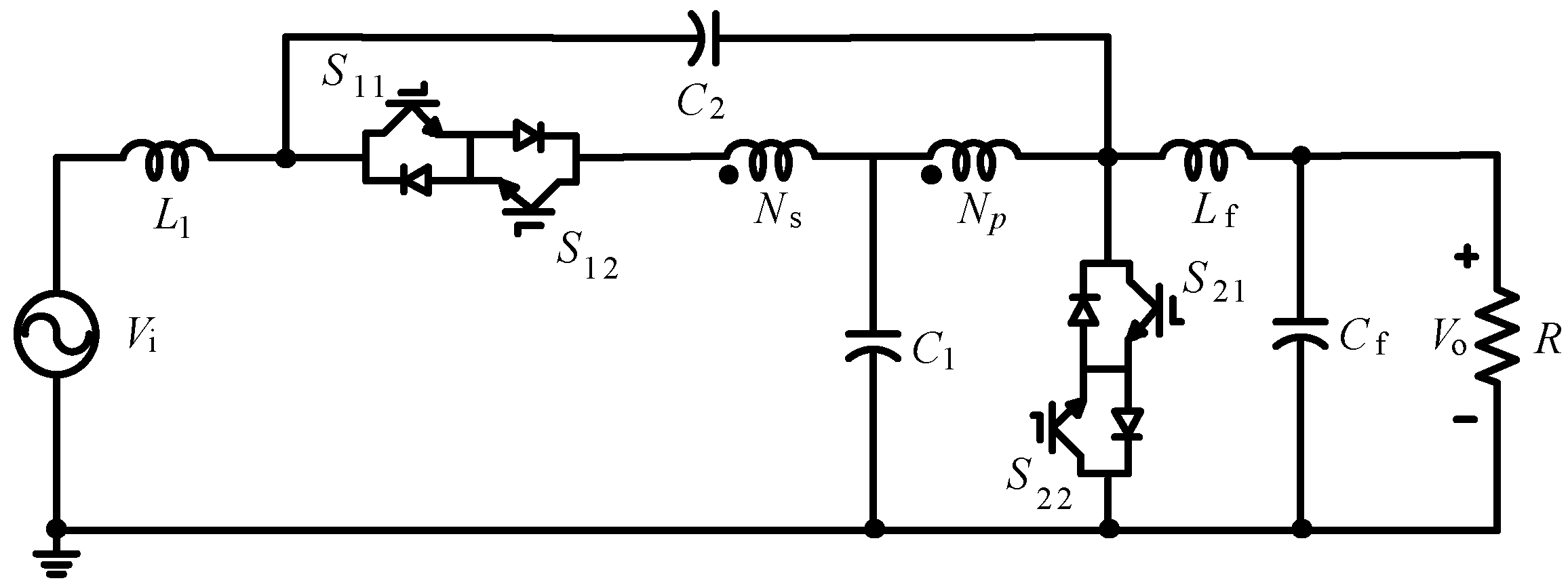
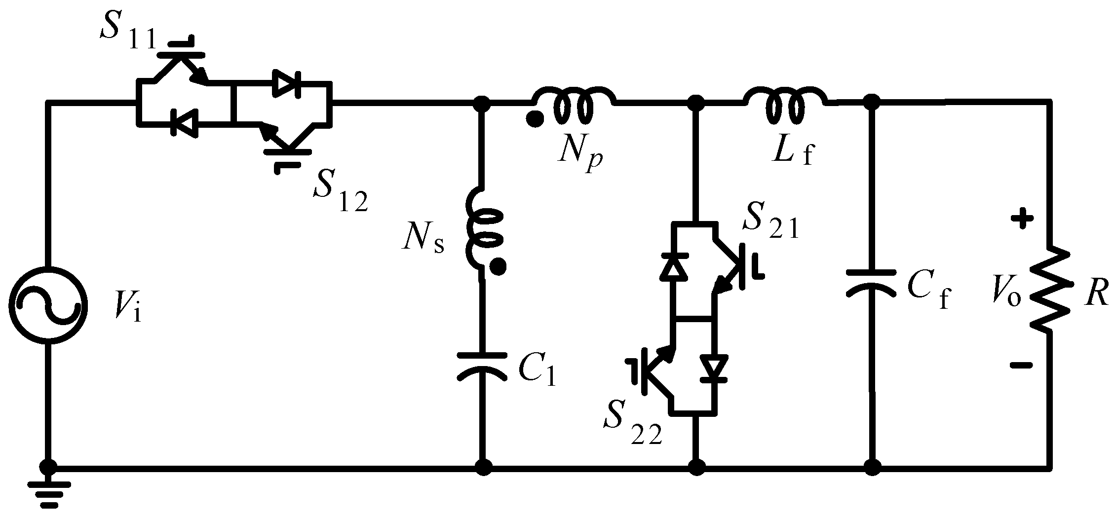
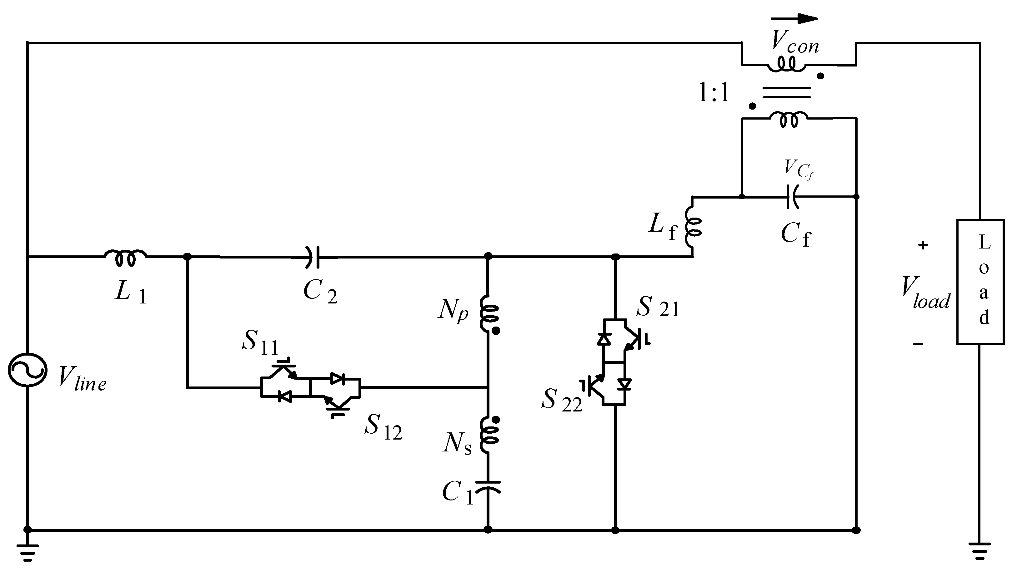
2. Trans-Inverse Magnetic Coupling Single-Phase AC-AC Converter

The presented trans-inverse magnetic coupling single-phase AC-AC converter is shown in Figure 3. The input inductor L1 is connected in series with the AC input source, resulting in a continuous and smooth current. The introduced topology exploits an impedance network, including an input inductor L1, a coupled transformer with the windings of NP-NS, and capacitors C1 and C2. The relationship between the transformer’s windings turns is N = NP/NS. Two power switches are used to transfer the power between the input and output sides bi-directionally. Each of the switches is a combination of two anti-parallel diodes and two back-to-back IGBTs or FETs. An output filter consisting of Lf and Cf is considered to decrease the ripples and harmonics. Hence, the proposed converter employs ten passive and active components, which is reasonable compared to the previous single-phase AC-AC converters. From Figure 3, it can be seen that the input and output sides have a common ground, which bring the advantages for the input and output waveforms.

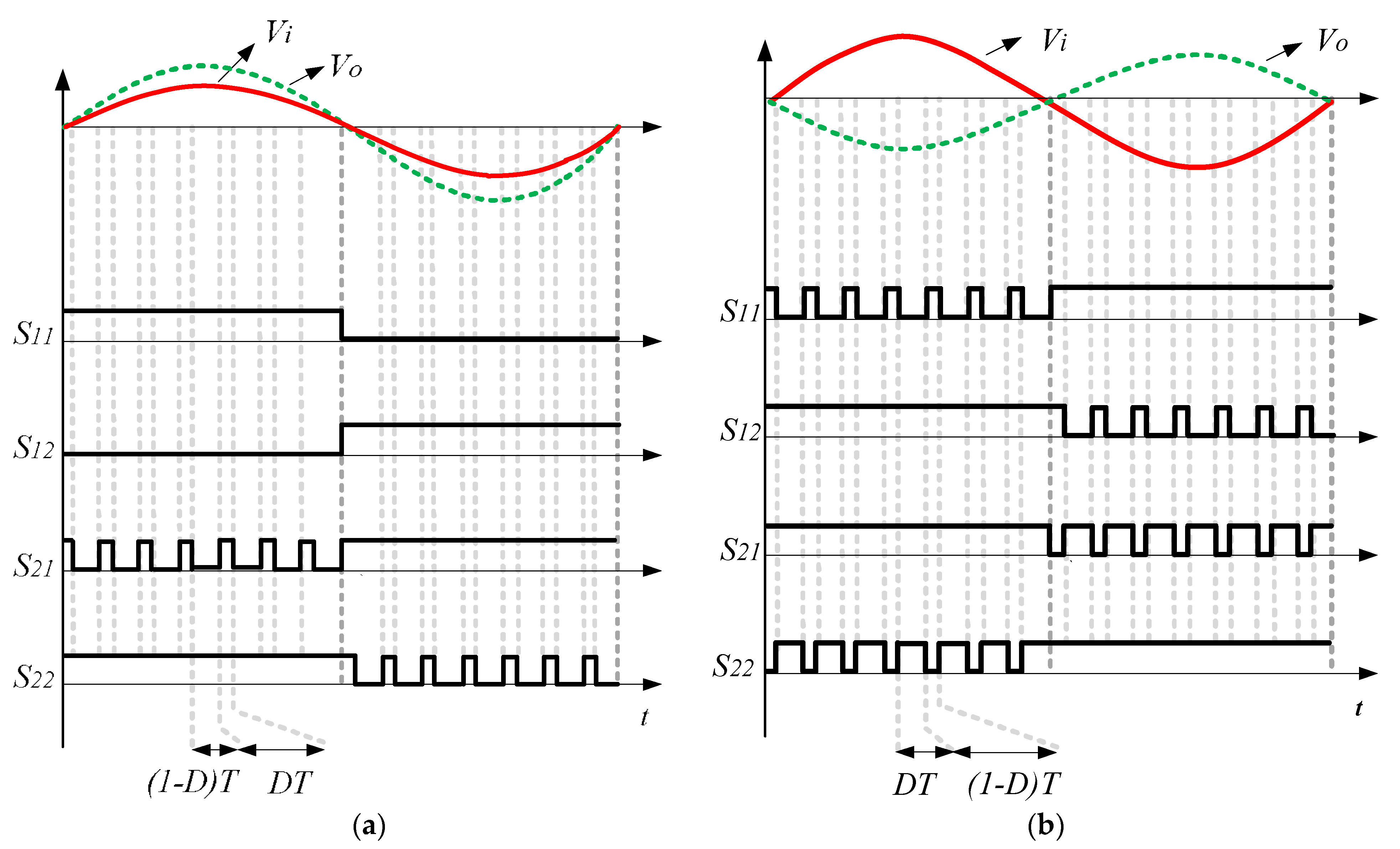
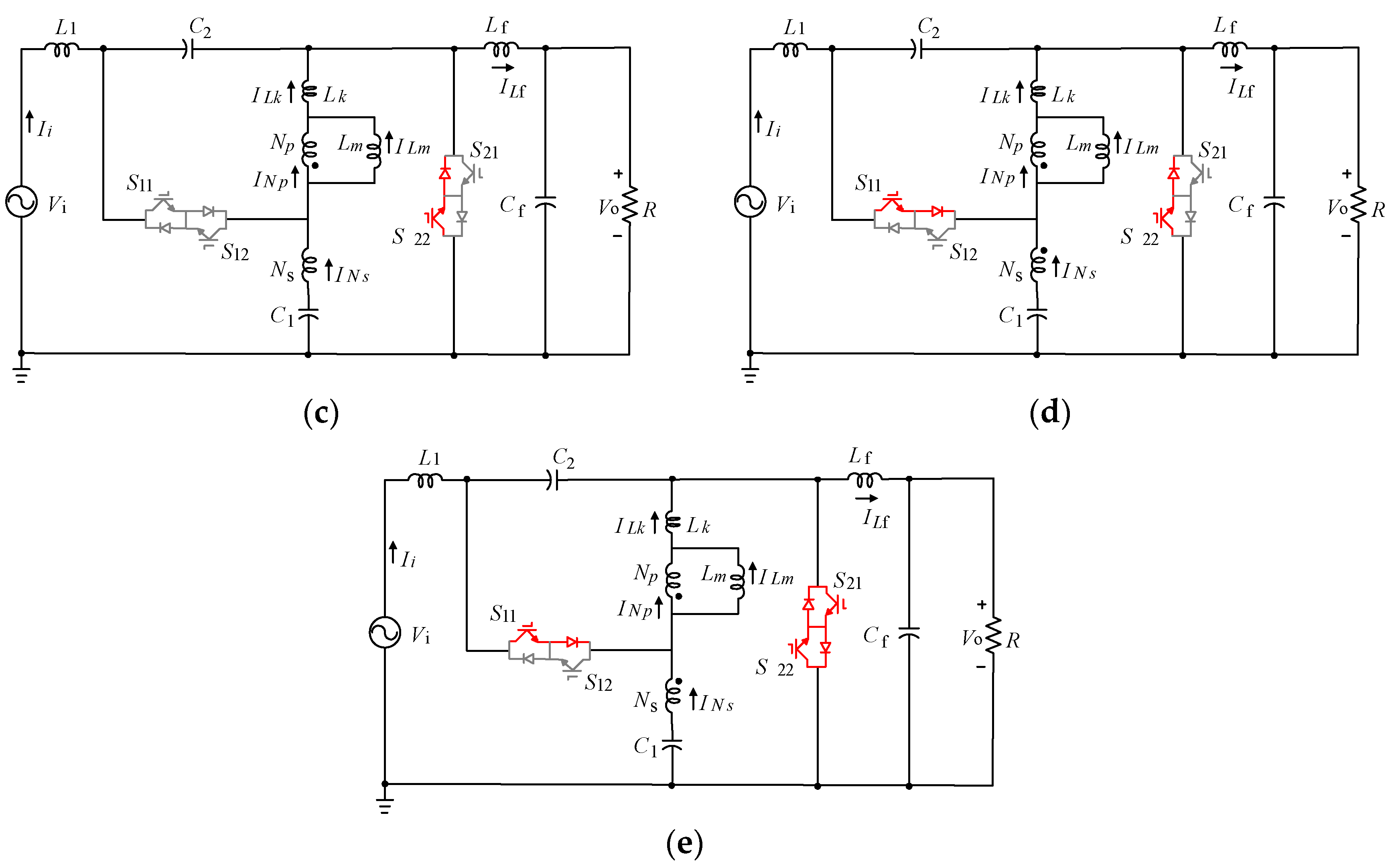
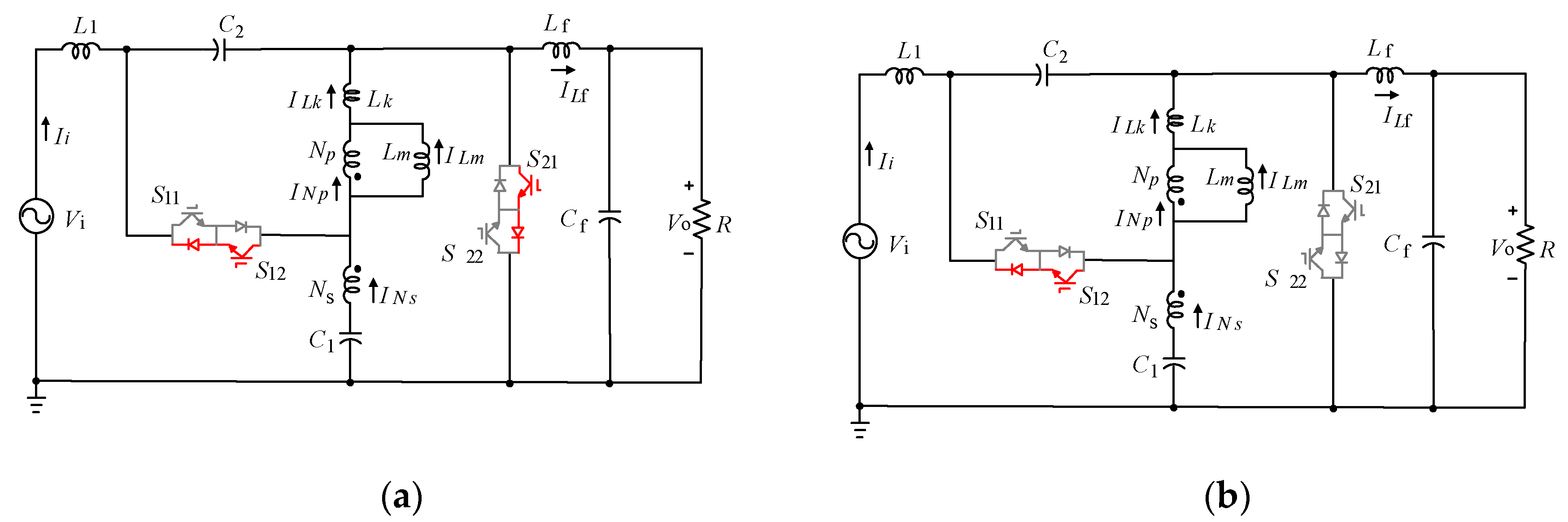
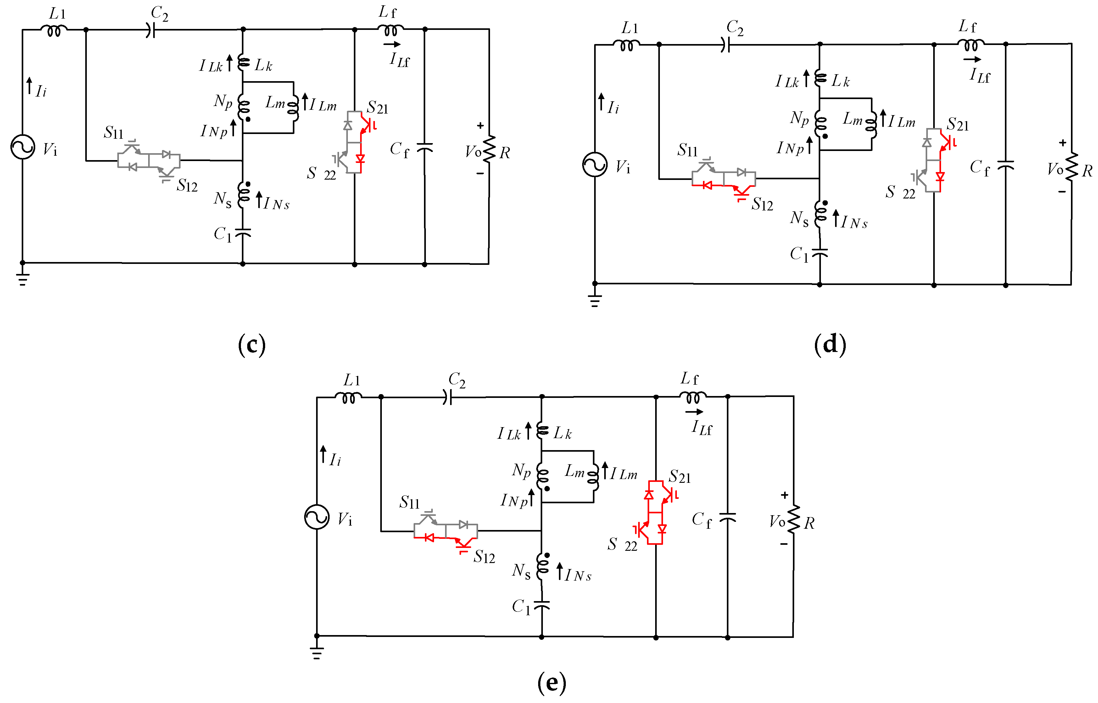
2.1. Commutation Strategy

Over the switching period, the power switches may sustain current and voltages spikes because of their overlap, dead-time effects, and instantaneous changes in capacitors’/inductors’ voltages/currents. Two ways can be applied to eliminate these destructive spikes: designing the snubber circuits or implementing a safe commutation strategy. Due to the complexity and cost increment and the efficiency reduction in the snubber circuits, implementing a safe commutation technique is considered a more efficient strategy. The switching pattern of the applied safe commutation method to the presented converter in boost in-phase mode and buck or boost out of phase mode is shown in Figure 4. To perform the mentioned commutation strategy, four switches must not be turned ON at the same time. Furthermore, the dead time for the switches must be considered in practice. From Figure 4a, for the positive input voltage, when the converter operates in boost in-phase mode, S 11 S 22 are switched on entirely, and S 12 S 22 are modulated complementary at a high frequency. For the negative input voltage and boost in-phase state, S 12 S 21 conduct thoroughly, while S 11 S 22 are modulated complementary at high frequency. In boost in-phase state and during the input voltage is positive/negative, we entirely turn OFF the S 12 / S 11 . Accordingly, semiconductors’ lifetime grows, and conducting losses are reduced dramatically. Additionally, the pulse width of S 21 and S 22 can directly change the voltage boost factor. As a result, by exploiting the presented coupled transformer, smaller pulse width of the switches can be applied to obtain high voltage boost ability. From Figure 4b, for boost/buck out-of-phase state, during the positive input voltage, S 11 S 22 are modulated complementarily, while S 12 S 21 conduct fully. Then, during the negative input voltage, S 11 S 22 are completely turned ON, and S 12 S 21 are modulated complementary.
The presented topology’s current paths in boost in-phase mode for the positive and negative input voltage are demonstrated in Figure 5 and Figure 6, respectively. From Figure 5, the operation intervals of the presented topology consist of a non-shoot-through state, dead time intervals, and a shoot-through state. Figure 5a shows the non-shoot-through mode when S11 is fully turned ON to conduct positive current from source to load, and S22 is conducting to remove commutation effects difficulty in a dead time interval, S21 is in OFF state, and as mentioned earlier, S12 is fully turned OFF. Three conditions happen before switching ON the output switches to reach the shoot-through mode during the dead time. According to Figure 5b, if Ii + ILkIlf > 0, S11 passes the current flow. If Ii + IlkIlf < 0, two conditions can occur; if ILk = ILm S22 conducts current flow that is demonstrated in Figure 5c, if ILk < ILm, the stored energy in Lm must be reduced through the S11 path. As shown in Figure 5d, this condition is kept until the save energy in Lm and Lk becomes equal, where Lm and Lk express magnetizing inductance and leakage inductance, respectively. Eventually, S21–S22 are turned ON to reach the shoot-through state, and S11 is switched ON for the commutation issue, shown by Figure 5e.
Figure 6 shows the operation intervals of the introduced topology in boost in-phase state for the negative input voltage. Figure 6a illustrates non-shoot-through mode, when switch S12 conducts to create a negative current flow and S21 is switched on because of removing the commutation difficulty. Based on indicated causes, S11 is entirely turned OFF. In order to provide shoot-through mode, three states can happen before switching on the S22 during dead time. According to Figure 6b, if Ii + IlkIlf < 0, S12 provides the negative current path. If Ii + ILkIlf > 0, there are two conditions based on the saved energy of Lk and Lm. If ILk = ILm the current path is provided through S21, which is shown in Figure 6c. From Figure 6d, if ILk > ILm S12 is turned ON in order to the stored energy of Lm and Lk to become balanced. Finally, S21 − S22 are turned ON to create the shoot-through state, and S12 is turned on to avoid commutation problems, as shown in Figure 6e.

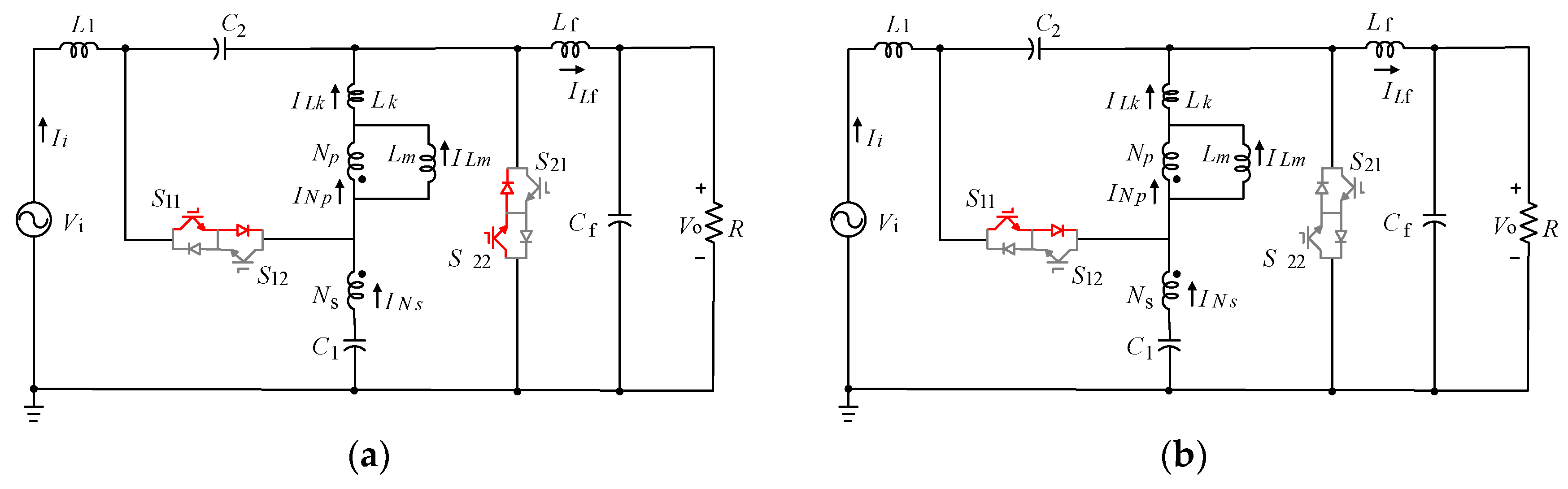
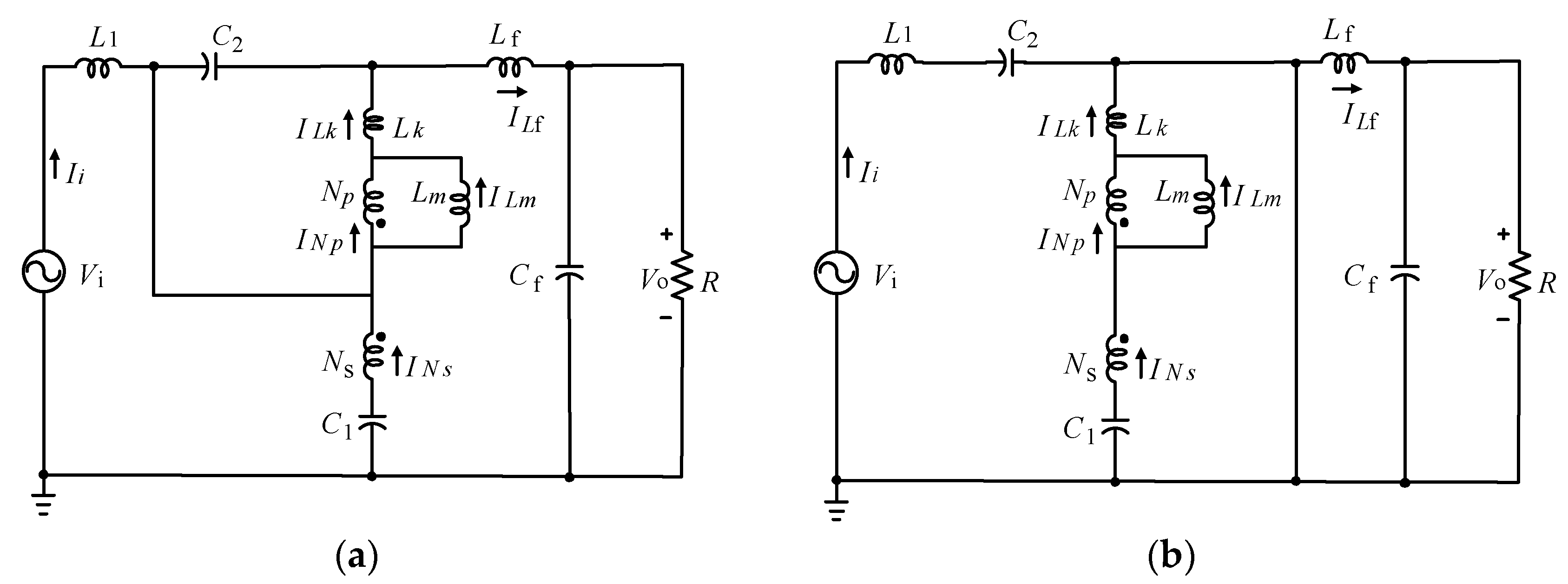
2.2. Circuit Analysis

The assumptions for the introduced topology analysis are considered as follows; it works in continuous conduction mode (CCM), the effects of the switches’ dead time are ignored, the switching frequency is higher than the source frequency. Likewise, the equivalent series resistance of capacitors, the parasitic resistance of inductors, the ON-resistance of the semiconductors are negligible. Additionally, the turns ratio (n) of the transformer and the coupling coefficient (k) are defined as:
n = V N p V N s = i N s i N p ,   k = L m L m + L k
Two operating modes are supposed in the steady-state analysis because of the ignorable effects of switches’ dead time: (1). non-shoot-through (NST) and (2). shoot-through (ST) states. Figure 7a,b show the equivalent circuits of the introduced converter in NST and ST states, respectively. According to Figure 7a, in NST mode, switch S1 ( S 11 S 12 ) is turned ON, and switch S2 ( S 21 S 22 ) is turned OFF. The time interval of this state is (1-D)T that D and T present the duty cycle and the switching period, respectively. So, by applying KVL and KCL, the equations are derived as (4). According to Figure 7b, in ST state, S2 (S21 − S22) is turned ON and switch S1 (S11 − S12) is turned OFF. In this state, DT is the time interval, and (5) can be obtained by KVL and KCL.
[ L 0 0 0 0 0 0 L m 0 0 0 0 0 0 L f 0 0 0 0 0 0 C 1 0 0 0 0 0 0 C 2 0 0 0 0 0 0 C f ] d d t [ i i ( t ) i L m ( t ) i L f ( t ) v C 1 ( t ) v C 2 ( t ) v o ( t ) ] = [ 0 0 0 1 k n 0 0 0 0 0 k 0 0 0 0 1 1 k n 1 1 0 1 0 0 0 1 n 1 n 1 n 0 0 0 0 0 1 0 0 1 R ] × [ i i ( t ) i L m ( t ) i L f ( t ) v C 1 ( t ) v C 2 ( t ) v o ( t ) ] + [ v i ( t ) 0 0 0 0 0 ]
[ L 0 0 0 0 0 0 L m 0 0 0 0 0 0 L f 0 0 0 0 0 0 C 1 0 0 0 0 0 0 C 2 0 0 0 0 0 0 C f ] d d t [ i i ( t ) i L m ( t ) i L f ( t ) v C 1 ( t ) v C 2 ( t ) v o ( t ) ] = [ 0 0 0 0 1 0 0 0 0 0 k n n k 0 0 0 0 0 0 1 0 n n 1 0 0 0 0 1 0 0 0 0 0 0 0 1 0 0 1 R ] × [ i i ( t ) i L m ( t ) i L f ( t ) v C 1 ( t ) v C 2 ( t ) v o ( t ) ] + [ v i ( t ) 0 0 0 0 0 ]
The average equations can be attained from (4) and (5) as follows:
[ L 0 0 0 0 0 0 L m 0 0 0 0 0 0 L f 0 0 0 0 0 0 C 1 0 0 0 0 0 0 C 2 0 0 0 0 0 0 C f ] d d t [ i i ( t ) i L m ( t ) i L f ( t ) v C 1 ( t ) v C 2 ( t ) v o ( t ) ] =   [ 0 0 0 D 1 k n D k n + D 0 0 0 0 0 ( D 1 ) K + D k n n k 0 0 0 0 1 D ( D 1 ) ( k n n ) 1 1 D n D n 1 D 1 0 0 0 1 n + D n D 1 D ( n 1 ) ( D 1 ) n 0 0 0 0 0 1 0 0 1 R ] [ i i ( t ) i L m ( t ) i L f ( t ) v C 1 ( t ) v C 2 ( t ) v o ( t ) ] + [ v i ( t ) 0 0 0 0 0 ]
According to average equation in each period and equaling the current average value of the capacitors and the voltage average value of the inductors to zero, we can get:
[ L 0 0 0 0 0 0 L m 0 0 0 0 0 0 L f 0 0 0 0 0 0 C 1 0 0 0 0 0 0 C 2 0 0 0 0 0 0 C f ] d d t [ i i ( t ) i L m ( t ) i L f ( t ) v C 1 ( t ) v C 2 ( t ) v o ( t ) ] = [ 0 0 0 0 0 0 ]
Hence, by solving (7), we have:
{ i i = n 1 n D + D   n 1 2 n D + D   v o R i o = i L f = v o R i L m = n 1 n D + D n D   ( i i i L f ) v C 1 = n k n D + k D k D 2 n D + n k   v i v C 2 = n D k D 2 n D + n k   v i v o = n k n D + k D   k D 2 n D + n k   v i
By supposing k = 1, the equation can be rewritten as:
{ v C 1 = n 1 n D + D n 1 2 n D + D   v i v C 2 = n D n 1 2 n D + D   v i v o = n 1 n D + D   n 1 2 n D + D   v i
Hence, the output voltage gain can be calculated as:
G v = v O v i = n 1 n D + D n 1 2 n D + D
From (10), we can get that the output voltage can be tuned by adjusting the transformer’s turns ratio (in the designing process) along with the duty cycle controlling. Additionally, if D < n 1 2 n 1 , the presented converter operates in the boost in-phase mode, and if D > n 1 2 n 1 , it operates in the buck/boost out-of-phase mode. Figure 8 demonstrates the output voltage gain versus the duty cycle of the presented converter with different transformer turn ratios. Obviously, in boost in-phase state, the introduced converter offers a higher voltage gain (in the same duty cycle) by reducing the turns ratio, which leads to size and cost reduction.

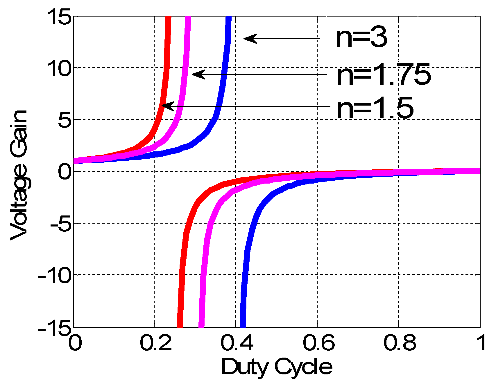
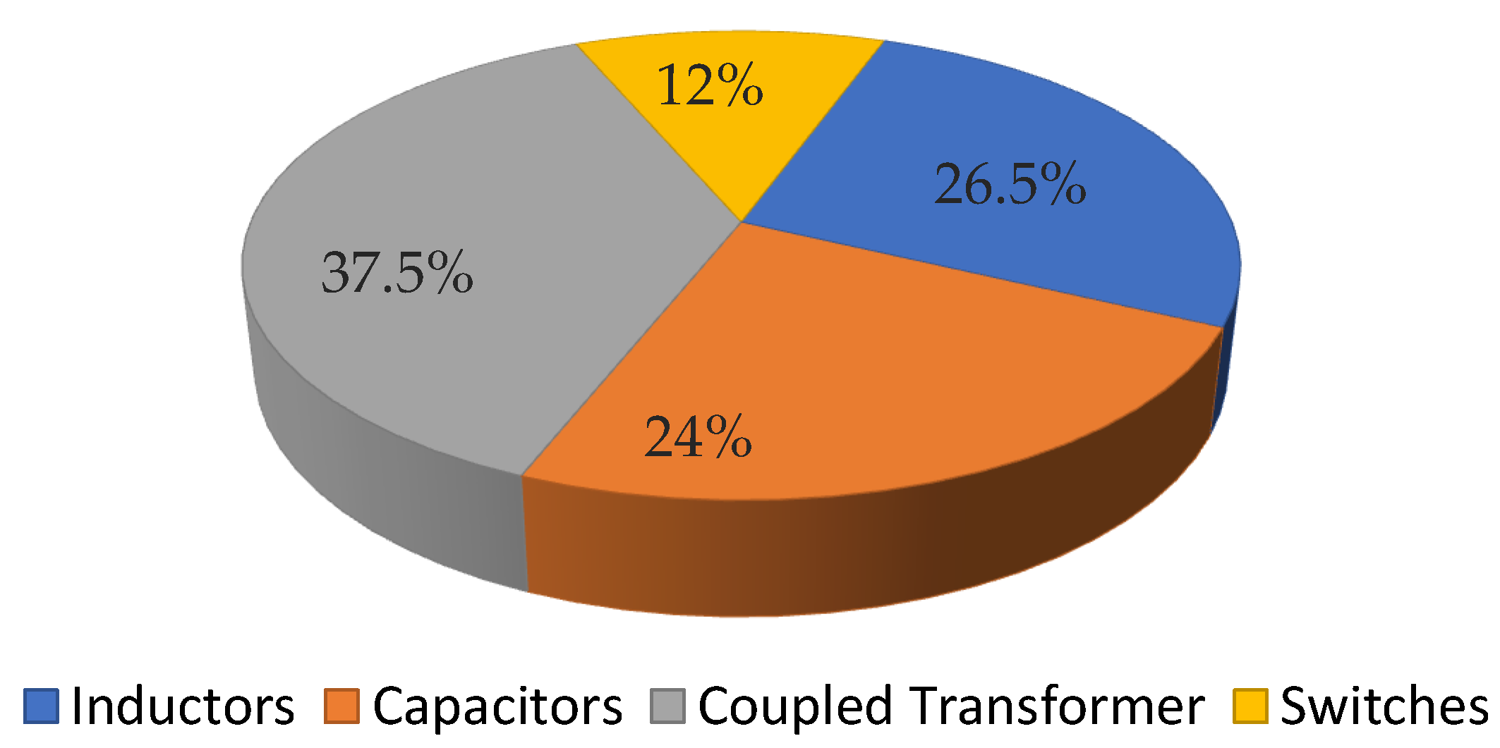
3. Parameter Design of the Proposed Converter

Firstly, magnetic components of the given topology are designed. Hence, the inductors parameters of the presented topology are designated based on their maximum current ripple in shoot-through state interval. Then, we have:
{ L = | V i   m a x + V C 2   m a x | d T Δ I i L m = | n V C 1   m a x n 1 | d T Δ I L m
If Δ I i and Δ I L m are considered as Δ I i x % i i and Δ I L m x % i L m , we can get:
{ L | V i   m a x + V C 2   m a x | D T x % i i = 2 V i 2 [ D n D + n 1 ] D T x % P O   [ D 2 n D + n 1 ] L m | n V C 1   m a x n 1 | D T x % i L m = 2 V i 2 T [ n 2 D ] [ n 1 n D + D + 2 D 2 ( n 1 ) ] x % P O [ n D + 2 D 2 ( n 1 ) ] [ n 1 ] [ D 2 n D + n 1 ]
It must be noted that i L m and i i represent current RMS values of Lm and L, respectively. Additionally, the capacitors’ parameters of the presented topology are selected based on their maximum voltage ripple in shoot-through state interval. Hence, we have:
{ C 1 = | n n 1 I L m | D T Δ v C 1 C 2 = | Ii | D T Δ v C 2
If Δ v C 1 and Δ v C 2 are considered as Δ v C 1 y % V C 1 and Δ v C 2 y % V C 2 , respectively, we have:
{ C 1 | n n 1 I L m | D T y % V C 1 = 2 P O [ n D + 2 D 2 ( n 1 ) ] [ D 2 n D + n 1 ] T y %   V i 2   [ ( n 1 ) 2 ] C 2   | Ii | D T y % V C 2 = 2 P O   [ D 2 n D + n 1 ]   T y %   V i 2   n
where, V C 1 and V C 2 present the RMS voltage of C1 and C2, respectively. Additionally, considering the RMS value of the input voltage (Vi), the maximum voltage stresses on bidirectional switches are derived by (15).
{ V S 1 , m a x = 2   n D 2 n D + n 1   V i V S 2 , m a x = 2   ( n 1 ) D 2 n D + n 1   V i

4. Application of the Proposed Converter

The proposed converter can be exploited as a dynamic voltage restorer. In this regard, the proposed converter operates as a line voltage conditioner by voltage sag and swell compensating. To explain more in details, the circuit of a dynamic voltage restorer based on the proposed converter has been shown in Figure 9. The input of the proposed converter is connected to the line voltage Vline in parallel. Furthermore, the output voltage of the converter Vcon is linked in series to the load voltage Vload and line voltage by an isolated transformer with 1:1 turn ratio. The presented system works in three operation modes according to the line voltage condition:
A. Bypass state
When the line voltage has a normal value, the proposed converter operates in bypass mode. In this mode, the proposed converter operates with D = 1 and the output voltage of zero. Additionally, the bidirectional switch S1 is fully turned OFF, and the bidirectional switch S2 is turned ON entirely.
B. Boost in-phase state
When the voltage sag occurs, the line voltage decreases to the lower value of demanded voltage. In this state, the proposed converter compensates the voltage sag amount. In this case, the proposed converter operates in boost in-phase mode. From the output voltage equation and by applying KVL to Figure 9, we have:
v l o a d = v l i n e + v c o n = v l i n e + ( n 1 n D + D   n 1 2 n D + D ) v l i n e = ( 2 n 2 3 n D + 2 D   n 1 2 n D + D ) v l i n e
C. Buck out-of-phase state
When the voltage swell happens, the line voltage increases to the higher value of normal voltage. In this mode, the proposed converter compensates the voltage swell amount. In this case, the proposed converter operates in buck out-of-phase state. From output voltage equation and by applying KVL to Figure 9, we can get:
v l o a d = v l i n e v c o n = v l i n e ( n + 1 + n D D   n 1 2 n D + D ) v l i n e = ( 2 n 2 3 n D + 2 D   n 1 2 n D + D ) v l i n e
Hence, we have the following relation between the switching duty cycle and transformer turn ratio for voltage sag and voltage swell conditions:
{ 0 D < n 1 2 n 1 , for   voltage   sag   condition 2 n 1 3 n 2 < D < 1 , for   voltage   swell   condition

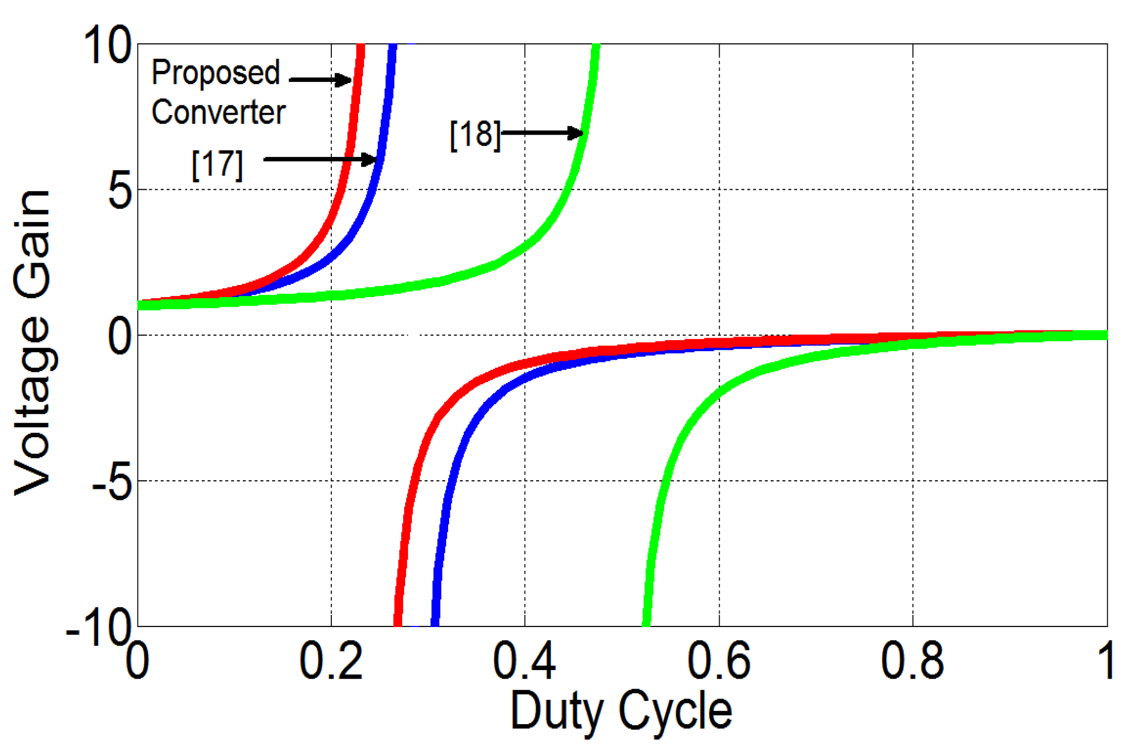
5. Comparative Analysis of the Proposed Converter

Contrary to the single-phase Γ -source AC-AC converter in [18], the presented converter offers a low continuous input current with low harmonics. Hence, it does not require any filter on the input side. Furthermore, contrary to the topology in [13,14], and [18], it shares the same ground between the input and output voltages. Unlike the single-phase AC-AC Trans Z-source and the modified single-phase ac-ac Trans Z-source topologies in [17,25], the introduced topology provides a high voltage boost factor by reducing the turns ratio instead of increasing it. From Figure 10, it can be obviously found that, compared with the Γ SC and ac Trans ZSC, the suggested converter presents a higher voltage boost factor with the same transformer’s turns ratio (n = 1.5) in a similar switching duty cycle. In addition, because of the unique feature of the exploited coupled transformer, using two coupled transformers is not needed like the topology in [19]. Finally, compared with the similar transformer-less single-phase AC impedance source converters, it supplies a higher voltage boost factor with shorter conducting pulses. According to the voltage gain equations in the selected topologies and by assuming Vo/Vi = 1.5 and n = 1.2 (for transformer types of the selected topologies), duty cycle for converters in [13,14,15,16,17,18,25], are 0.25, 0.21, 0.28, and 0.15, respectively.
The proposed converter provides the same output voltage gain with the duty cycle of 0.05. Hence, by utilizing the presented safe commutation strategy, the high output voltage can be attained by a low duty cycle and short time duration of switch conduction. It can play a significant role in the efficiency saving. Table 1 presents a brief comparison of the proposed converter and the selected topologies.

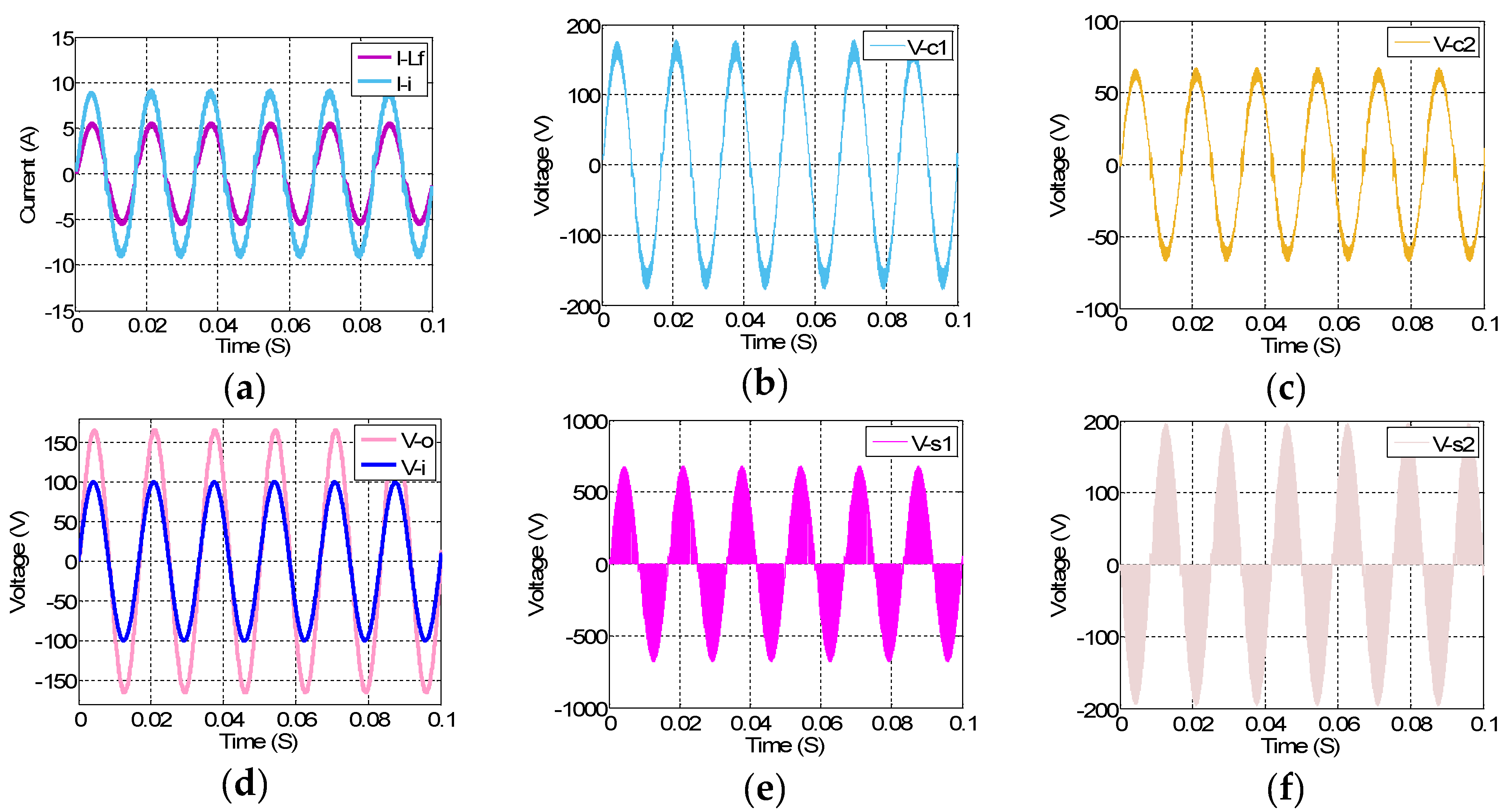
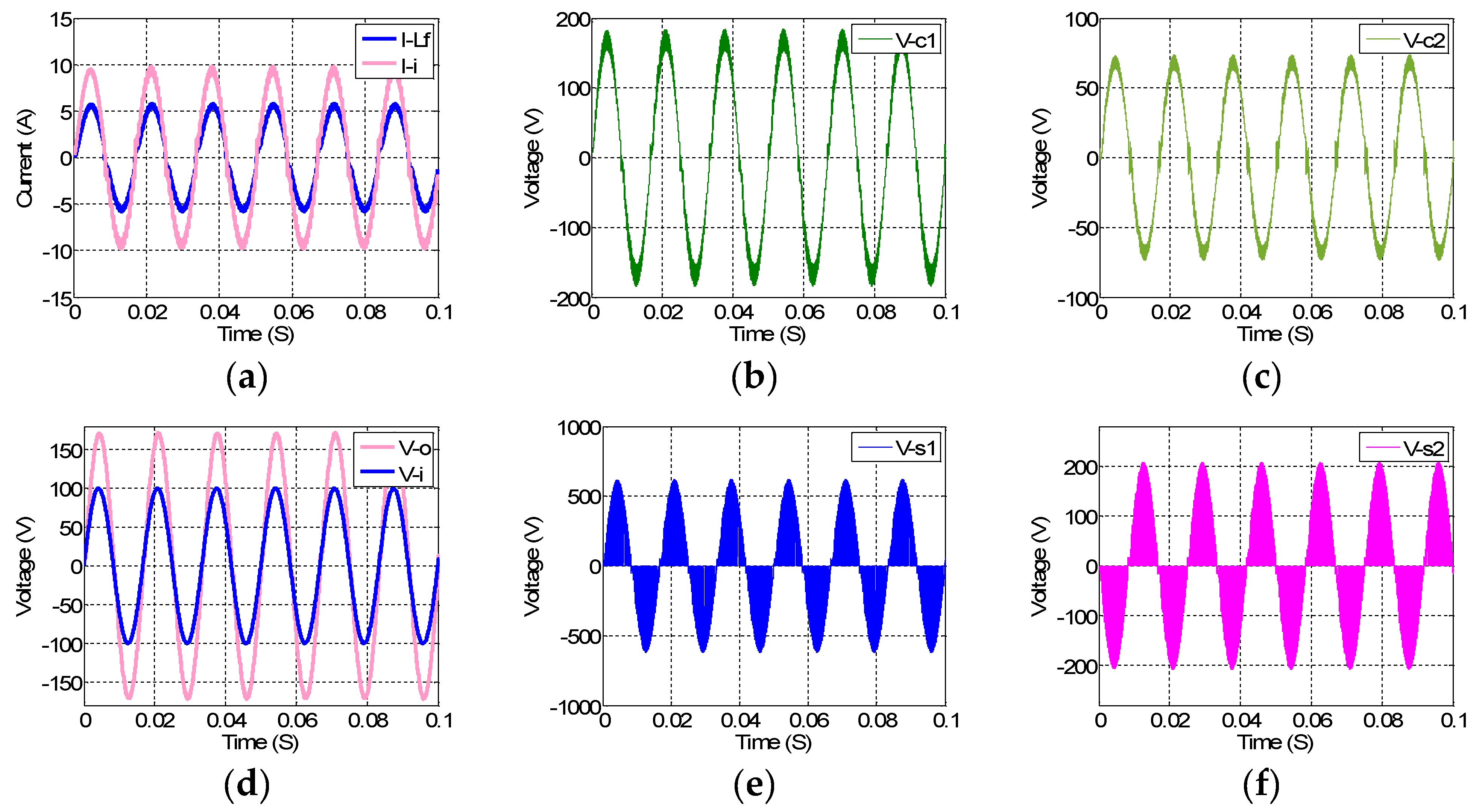
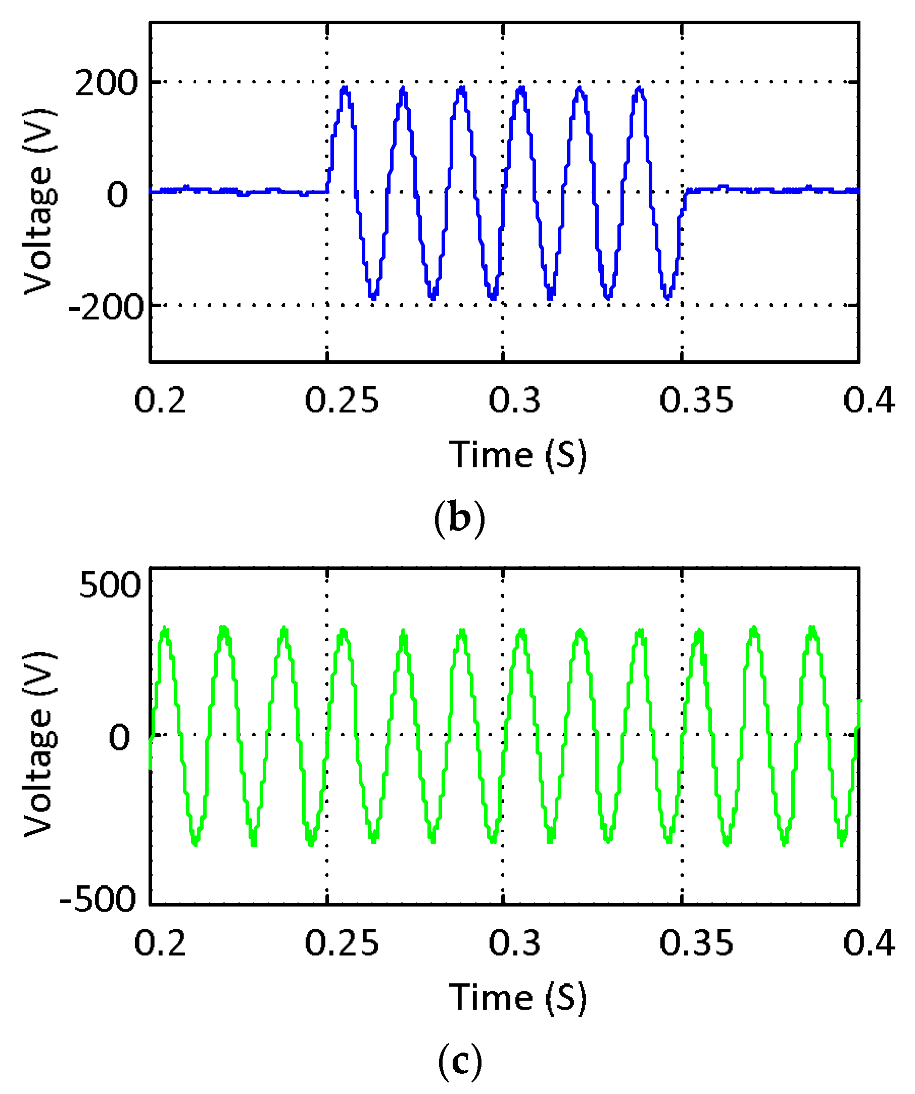
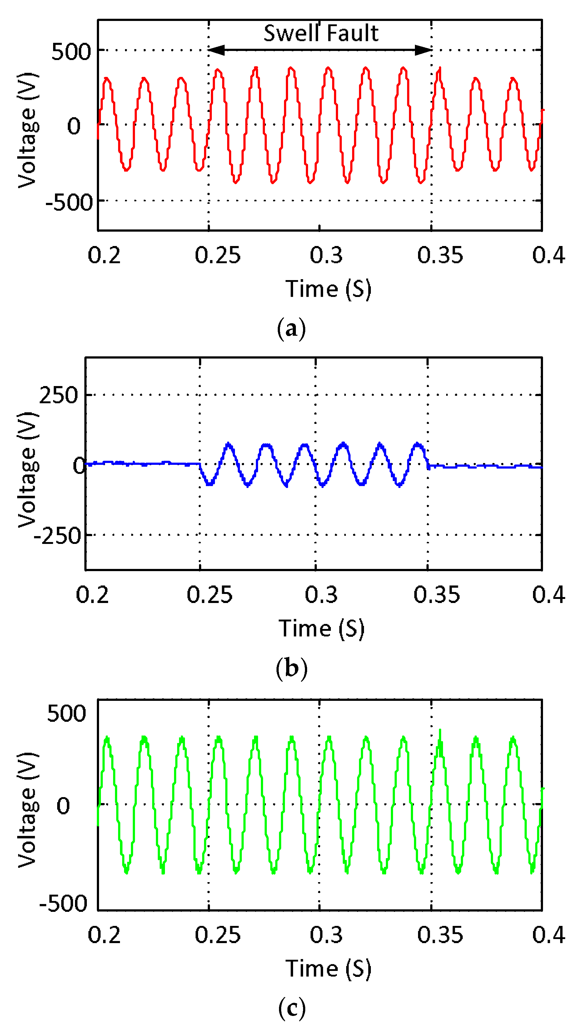
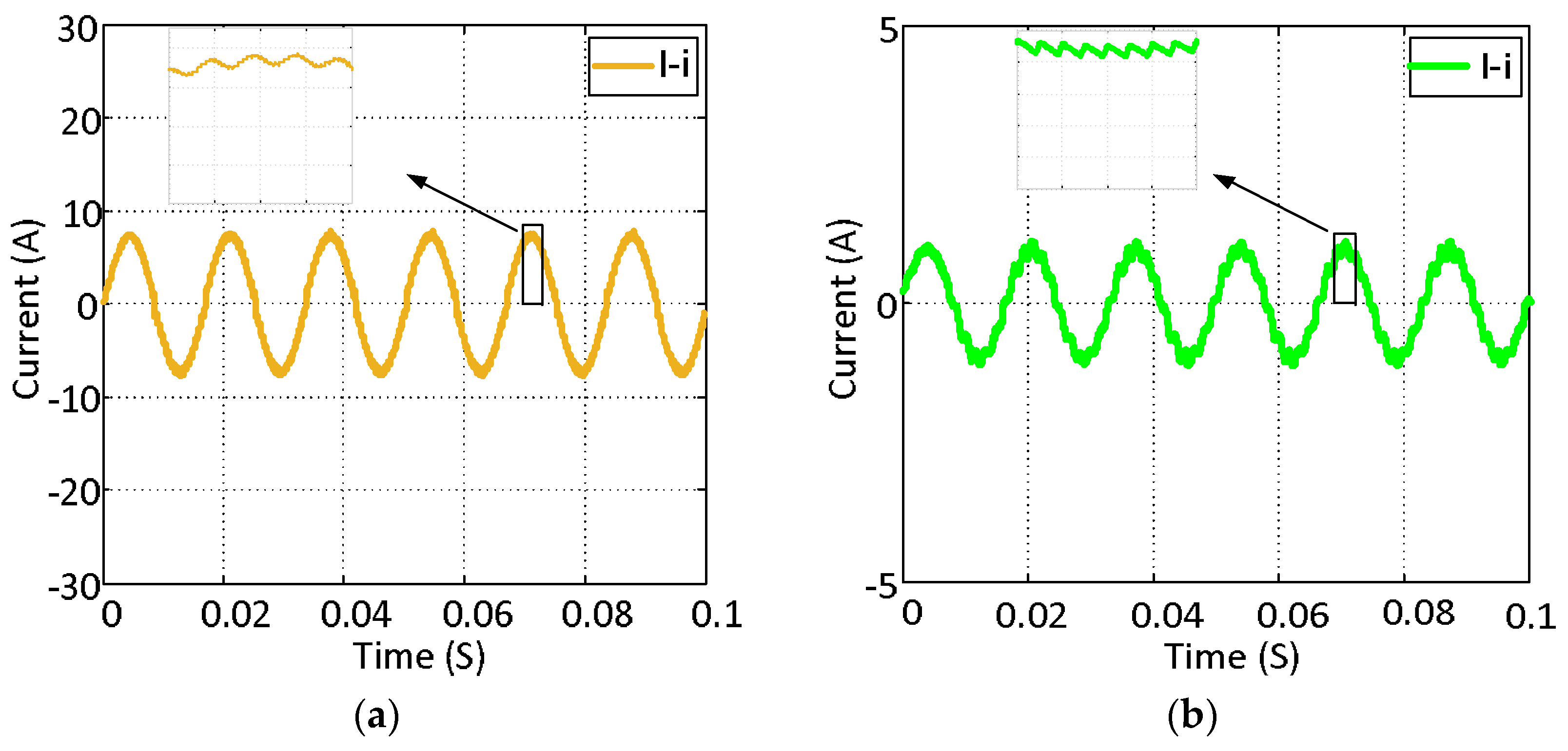
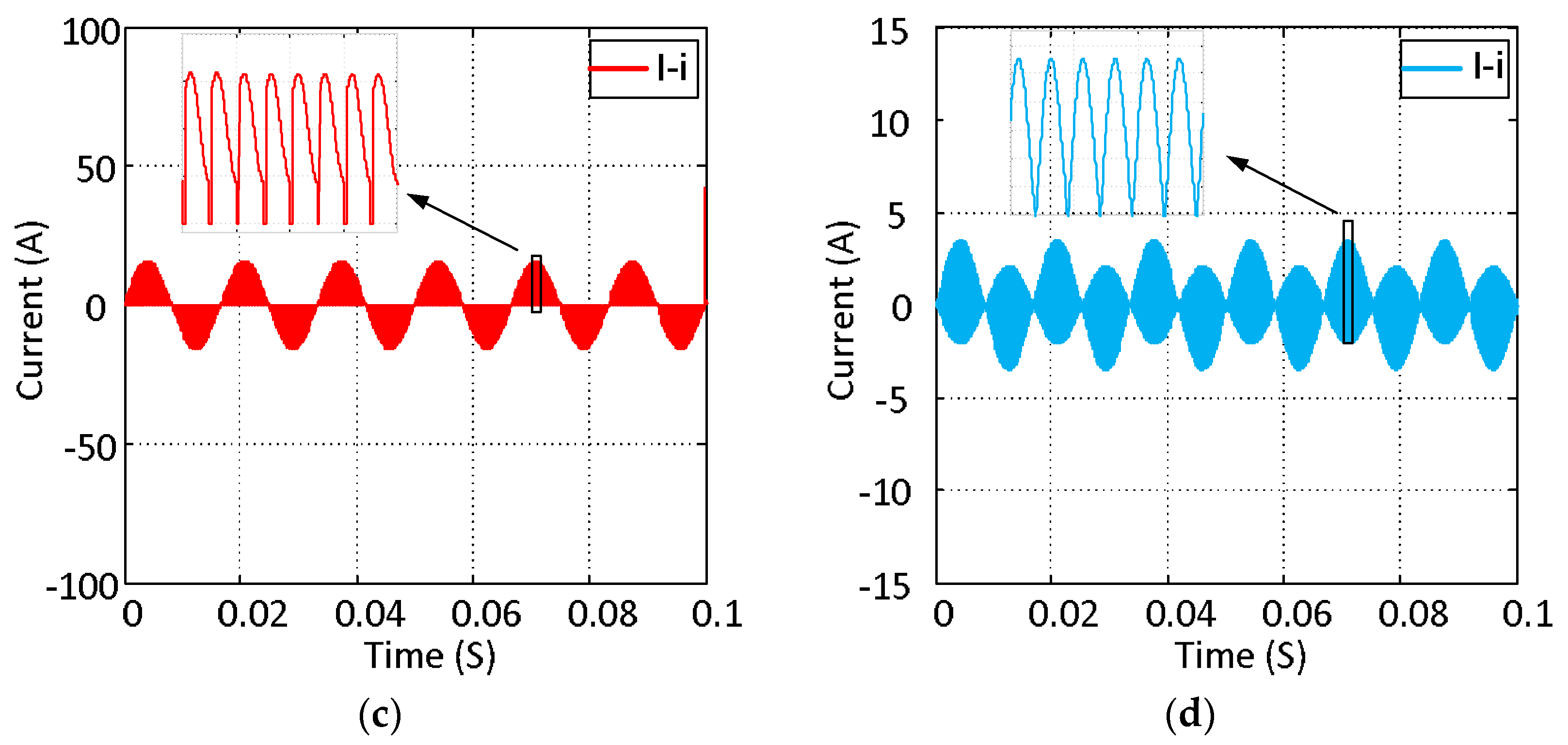
6. Simulation Results

To verify the design and operation of the proposed single-phase AC-AC converter, it is simulated in MATLAB/SIMULINK environment. The properties of the suggested topology in terms of circuit components and its operation modes are assumed as follows: the circuit components including capacitors (C1 = C2 = 6.8 µF, Cf = 47 µF) and inductors (Lf = 1.2 mH, LM = 0.8 mH, and L = 1 mH) are selected based on the mentioned design considerations. Notably, the coupling sufficient has been supposed k = 1. The structure of bidirectional power switches is simulated by using two back-to-back integrated MOSFETs. Notably, the input voltage and switching frequency of this study are 20 kHz and 60 Hz, respectively. Accordingly, the response of the proposed topology for both boost-in-phase and buck-out-of-phase operating modes with different conditions are investigated and the results are presented in the following.
The simulation results of the proposed converter in boost in-phase state with n = 1.5, D = 0.1, and R = 30 Ω are illustrated in Figure 11. As can be seen in Figure 11a, the input current is sinusoidal and continuous. From the theoretical results, the peak value of the input current, output current, voltage across C1, voltage across C2, output voltage, and voltage across S1 and S2 are approximately 7.5 A, 5 A, 150 V, 50 V, 150 V, 500 V, and 165 V, respectively, which can be verified by Figure 11a–f.
As mentioned in previous sections, the proposed topology is a trans- inverse magnetic coupling converter. So, by decreasing the transformer’s turns ratio the voltage boost factor must be increased. The operation of the proposed converter when the coupling ratio (n) was changed to 1.4 is studied and the simulation results of the boost in-phase state are shown in Figure 12. According to the mathematical equations, the peak value of the input current, output current, voltage across C1, voltage across C2, output voltage, and voltage across S1 and S2 are approximately 8.85 A, 5.4 A, 163 V, 63 V, 163 V, 630 V, and 180 V, respectively, which can be identified by Figure 12a–f. Moreover, the proposed converter’s output voltage can be controlled by adjusting the switching duty cycle, too. To verify this case, the proposed converter is simulated with n = 1.5, D = 0.12, and R = 30 Ω and the results are depicted in Figure 13. It can be understood that the output voltage can be raised by increasing the switching duty ratio. In this case, the peak value of the input current, output current, voltage across C1, voltage across C2, output voltage, and voltage across S1 and S2 are approximately 9.63 A, 5.7 A, 170 V, 70 V, 170 V, 570 V, and 190 V, respectively, which can be validated by Figure 13a–f. On the other hand, the proposed converter has high voltage buck ability at the same time. In order to assess the buck out-of-phase operating mode performance of the proposed AC-AC topology, it is simulated with n = 2, D = 0.8, and R = 2 Ω. The simulation results of this study are demonstrated in Figure 14. From the mathematical equations, the peak value of the input current, output current, voltage across C1, voltage across C2, output voltage, and voltage across S1 and S2 are about 1 A, 7 A, 14 V, 114 V, 14 V, 141 V, and 70 V, respectively, which can be identified by Figure 14a–f.
Figure 15 and Figure 16 show the simulation results of the presented dynamic voltage restorer based on the proposed converter with n = 1.5. A proportional integral (PI) controller has been utilized to adjust the load voltage. Figure 15a depicts the line voltage with an RMS value of 220 V when 60% voltage sag occurs at 0.25 s to 0.35 s. It is seen that the peak value of the line voltage decreases from 311 V to 125 V. Figure 15b demonstrates that when the line voltage is normal, the proposed converter operates in a bypass state, and when voltage sag happens, it operates in boost-in-phase mode. Figure 15c shows the line voltage without the fault effects. Figure 16a shows the line voltage under 25% voltage swell. It can be seen that the peak value of the line voltage rises from 311 V to 388 V. Figure 16b shows the output voltage of the proposed converter. It can be clearly seen that in the normal value of the line voltage, the proposed converter operates in bypass mode, while in the voltage swell period; it operates in buck out-of-phase mode to reduce the line voltage to its demanded value. So, the load voltage is maintained at the normal level, as can be seen in Figure 16c.

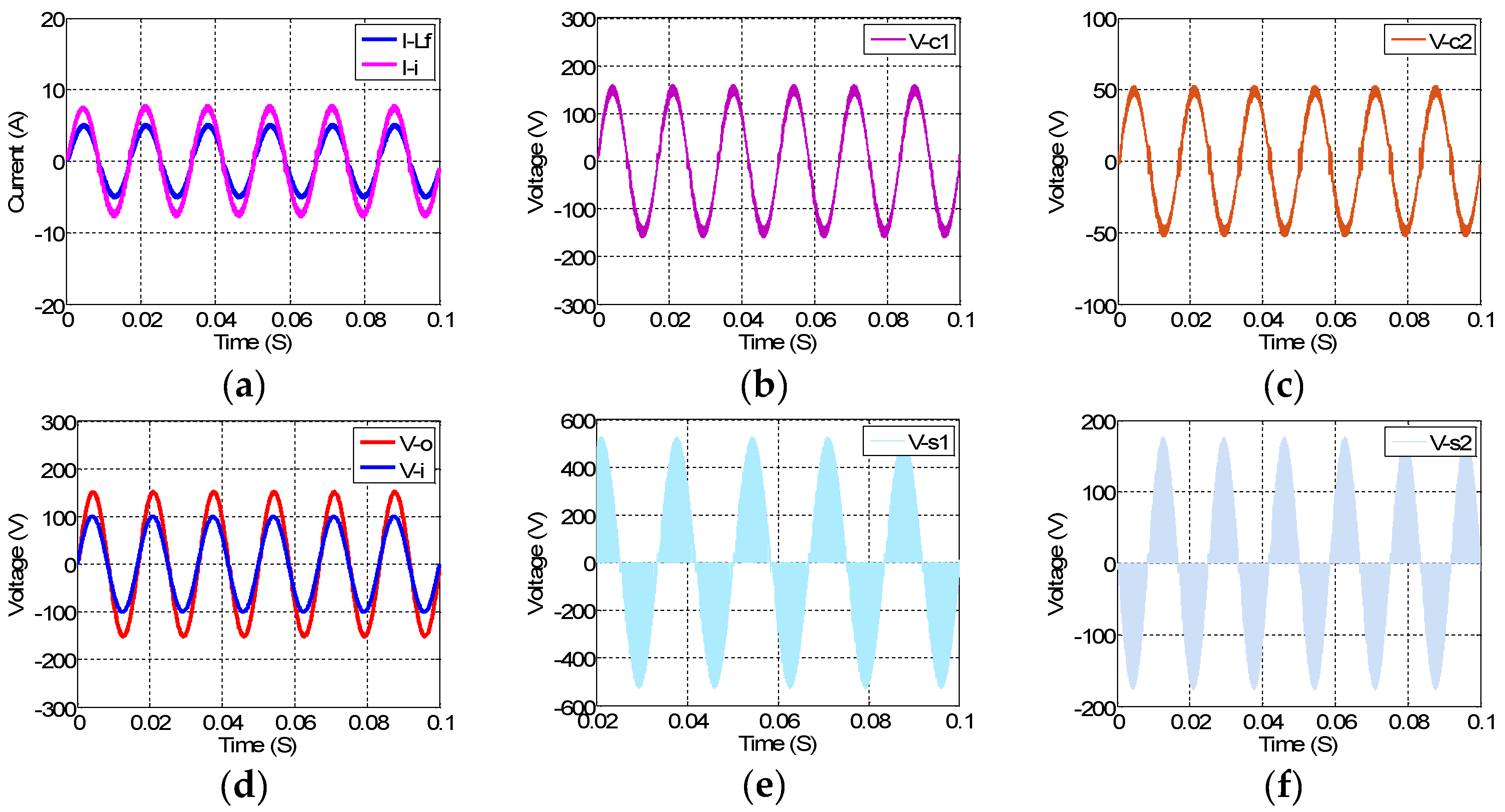
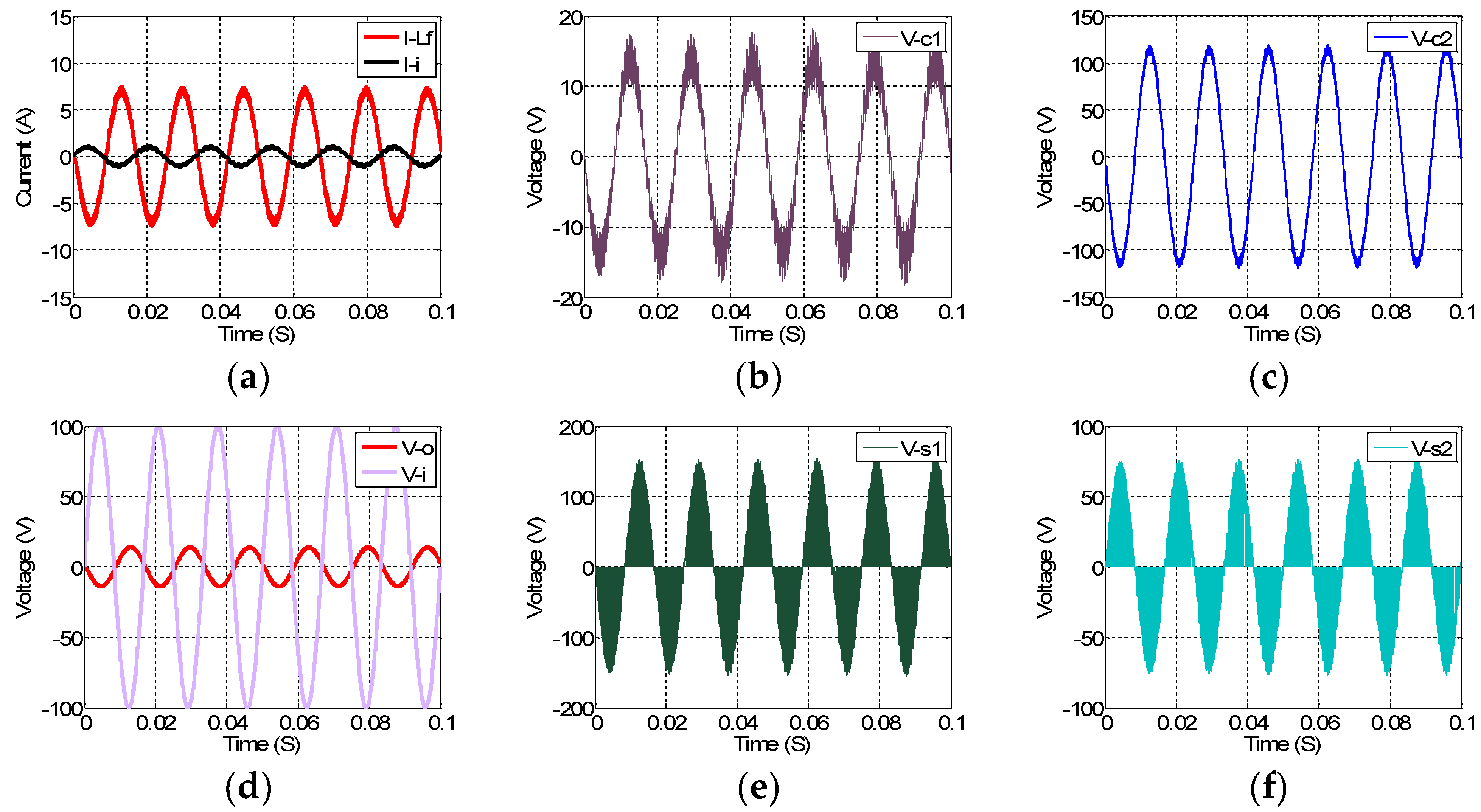
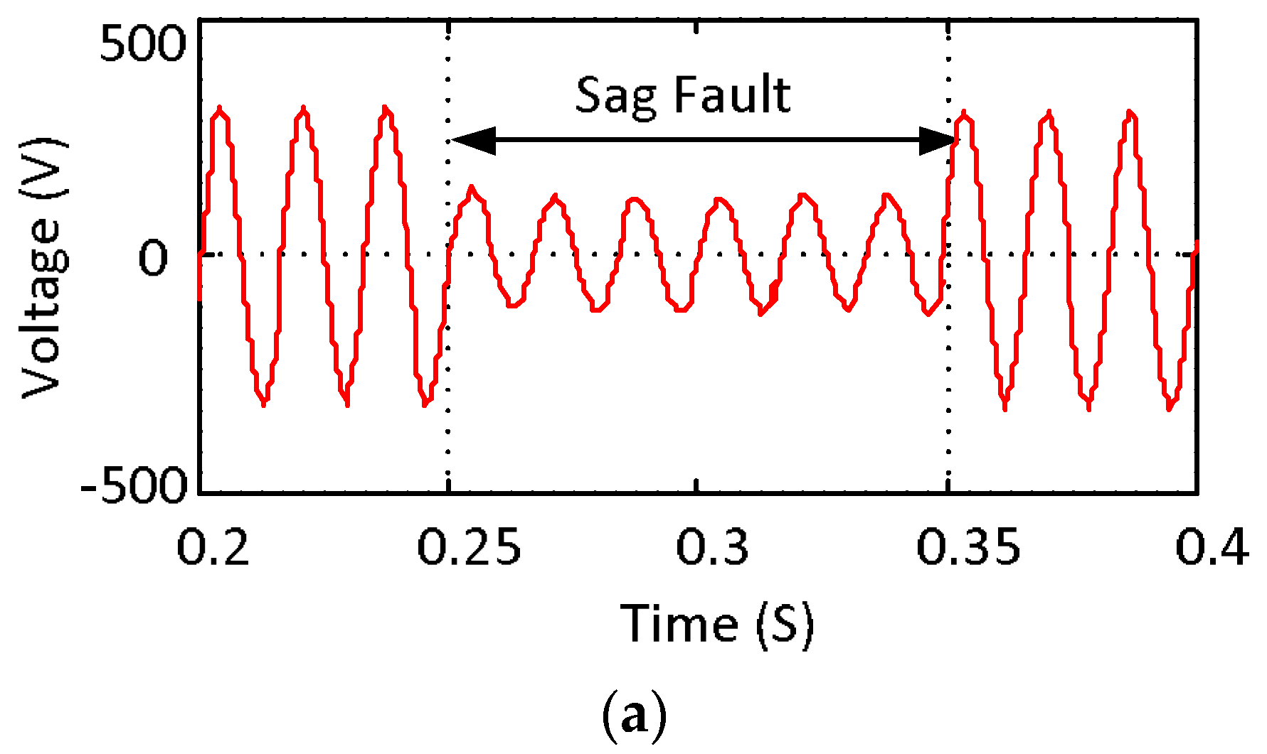
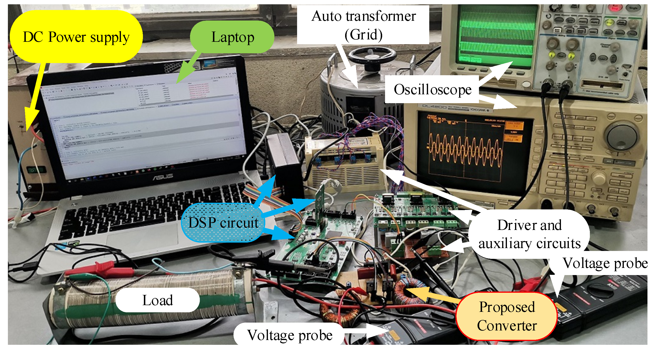
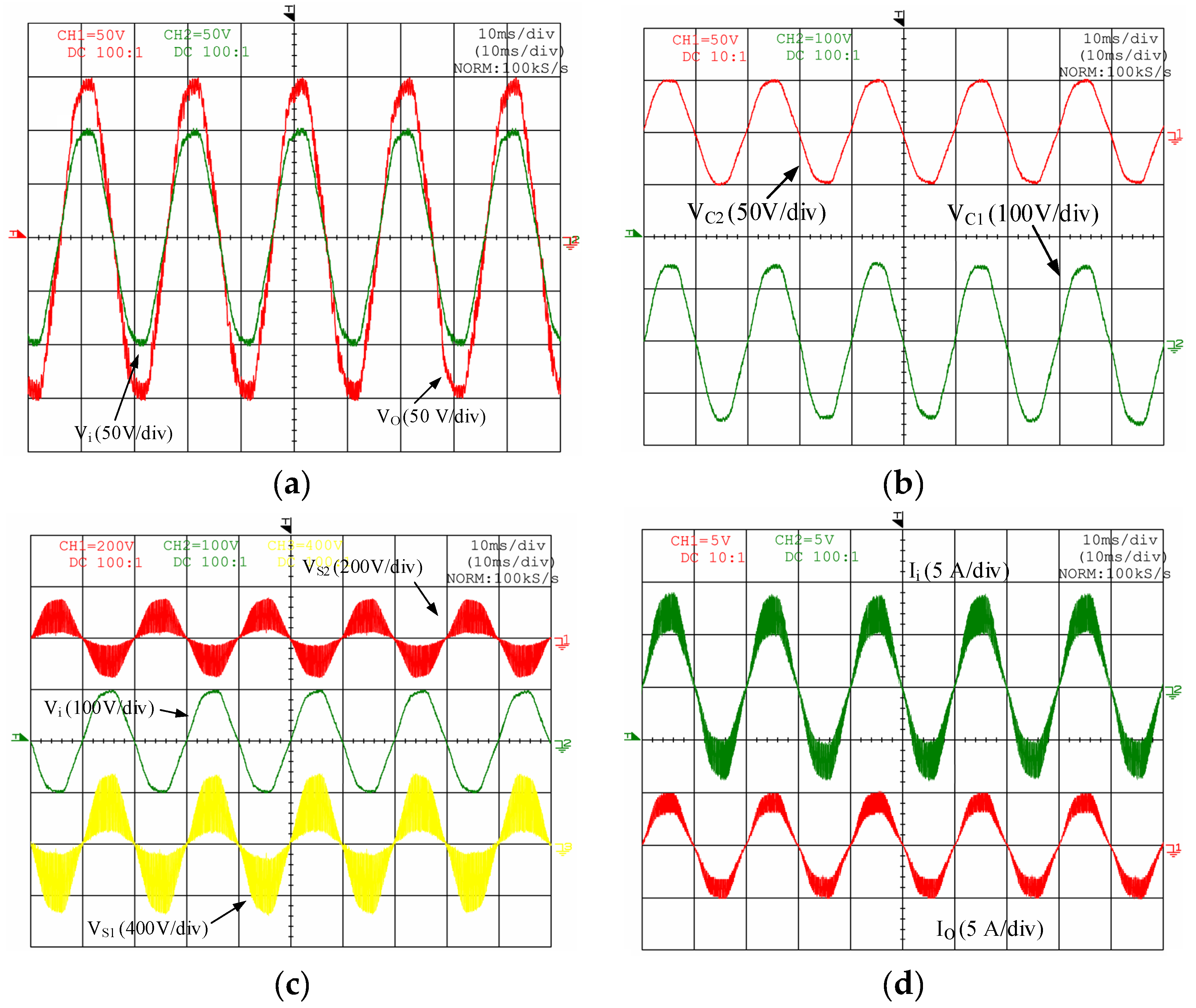
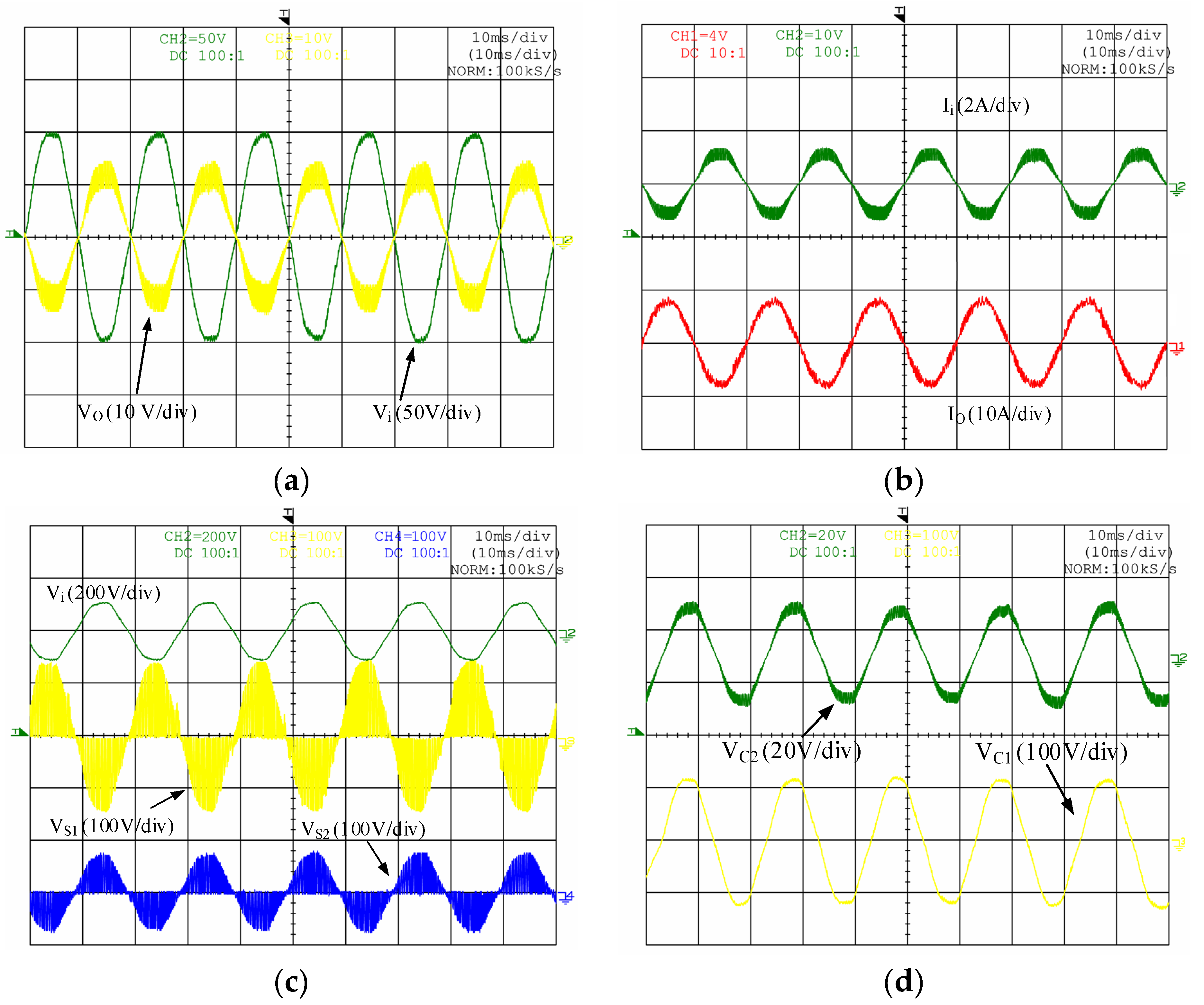
7. Experimental Results
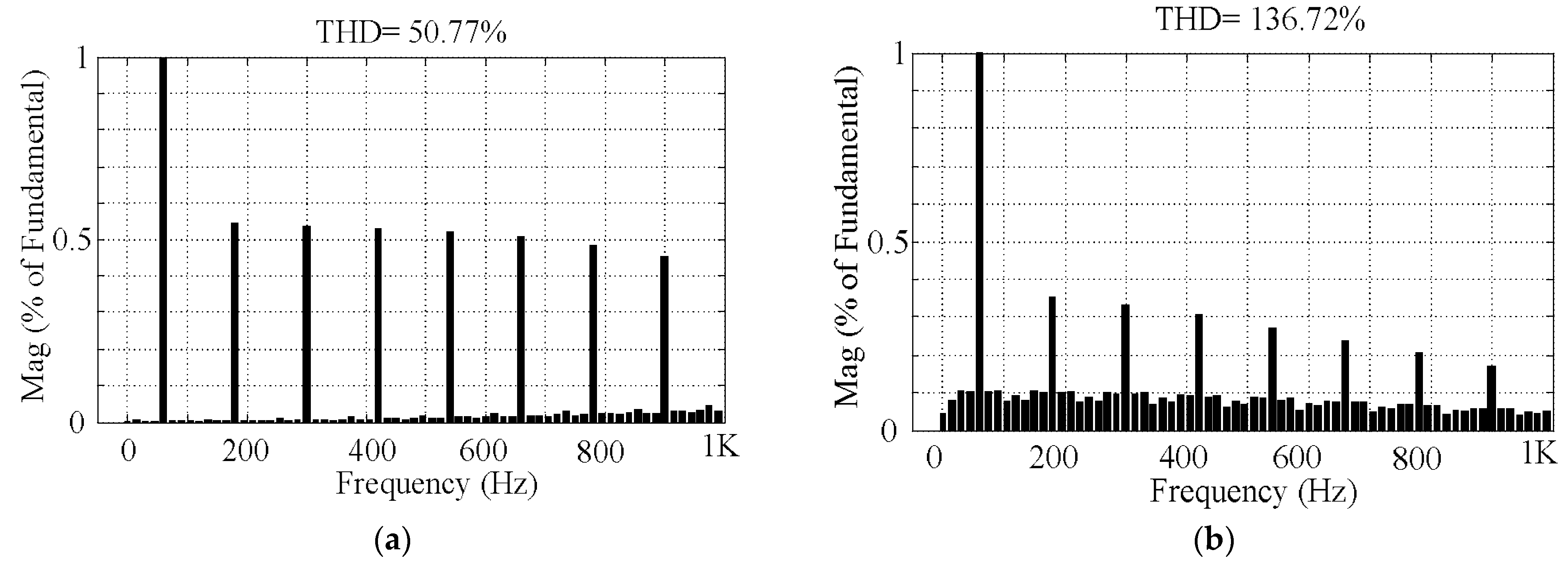
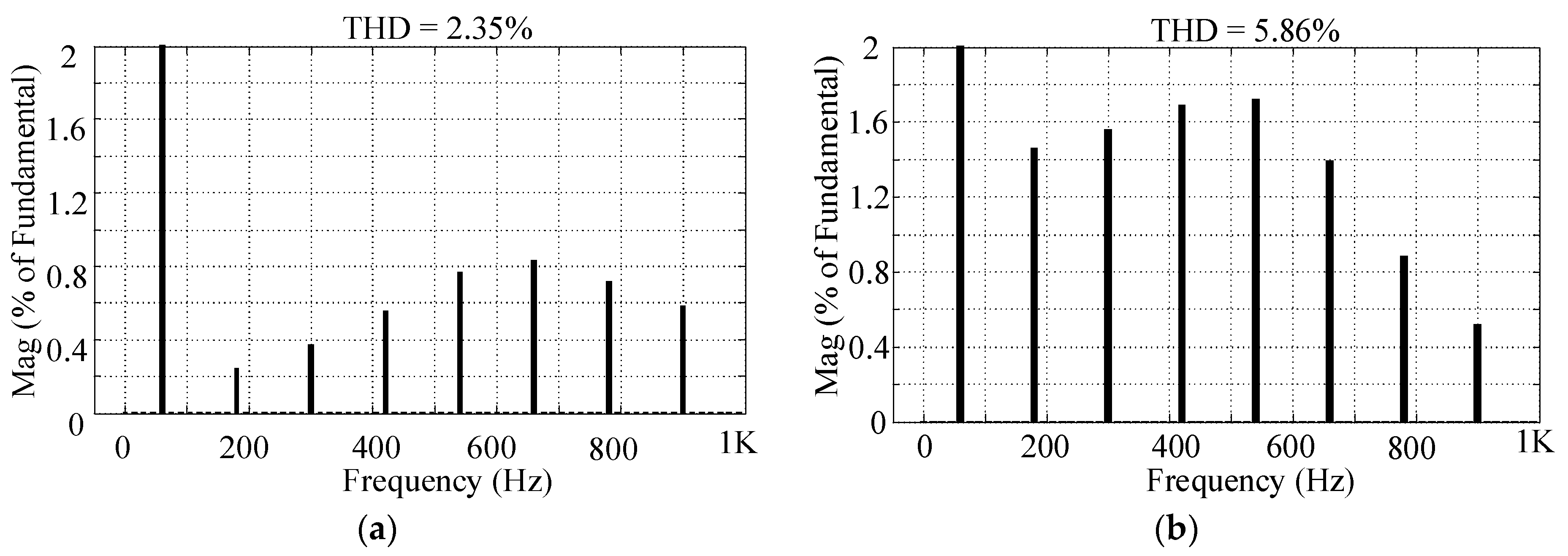
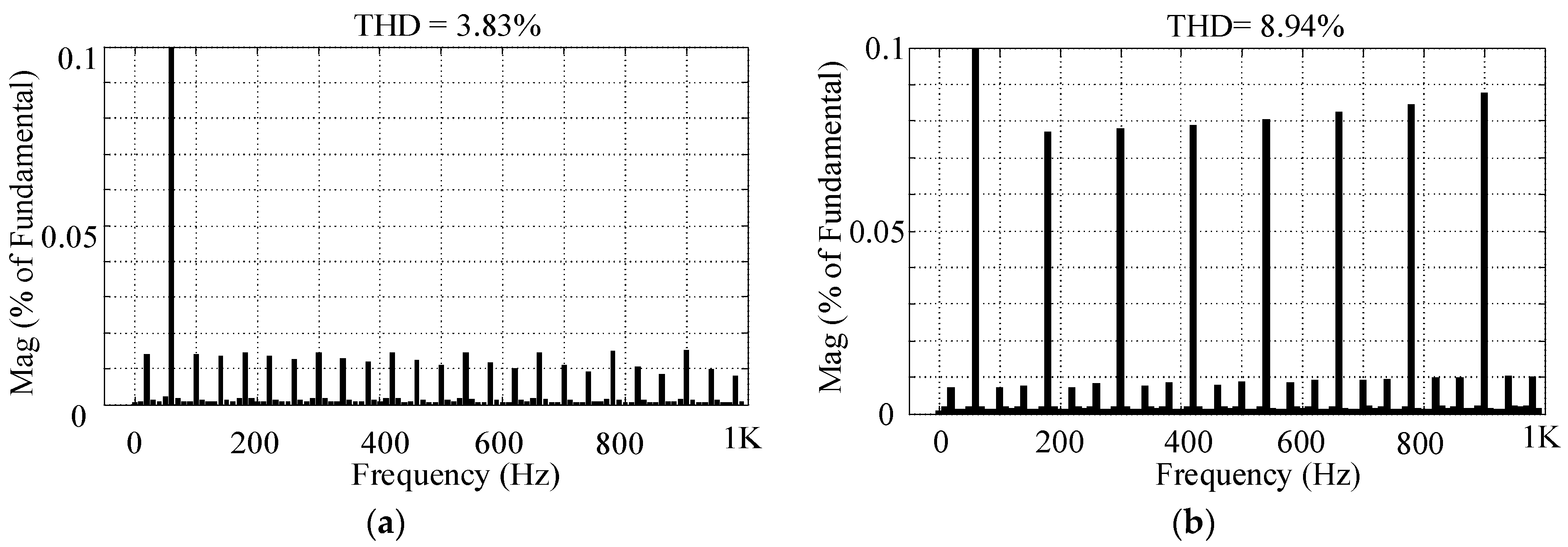
The circuit design’s feasibility and simulation results verification are examined by implementing a single-phase laboratory prototype. The picture of the test system is presented in Figure 17, and its properties are brought in Table 2. In order to perform the described safe-commutation strategy, a digital signal processor (DSP) was used. Additionally, the structure of each bidirectional switch was formed by using two back-to-back Power MOSFETs. A high-frequency coupled inductor with a coupling coefficient of almost one (k = 1) was designed.
To confirm the simulation results, both boosting and buck mode operations of the suggested topology are examined and the results are presented in Figure 18 and Figure 19, respectively. In this regard, to study the operation of the proposed single-phase AC-AC converter in boost in-phase state with D = 0.1, are illustrated in Figure 18. The turns’ numbers of the primary and secondary sides are 30 and 20, respectively, which results in a turn ratio of 1.5. Additionally, the resistive load is R = 30 Ω. The sinusoidal input and output voltage waveforms can be seen in Figure 18a. Additionally, it is clear that the output voltage can maintain the phase angle with the input voltage well. From (8), the peak value of the output voltage is attained 150 V, which can be identified in Figure 18a and (19).
v o p k = n k n D + k D k D 2 n D + n k   v i p k = 1.5 1 0.15 + 0.1   0.1 0.3 + 1.5 1 × 100 = 150   V
Besides, the voltages of the circuit capacitors are illustrated in Figure 18b. From (8), the peak value of the voltage stress across the capacitors C1 and C2 are 150 V and 50 V, respectively, which can be verified by Figure 18b. This case can be utilized for 50% voltage sag compensation. The voltage stress over the power switches accompanied by the input voltage is presented in Figure 18c. The peak values of the voltage stress across the S1 and S2 are about 500 V and 166 V, respectively, which can be clarified by Figure 18c. Additionally, by exploiting the presented safe commutation strategy, voltage spikes across the power switches are removed. Then, the converter’s input and output current waveforms are presented in Figure 18d. From the obtained current equations, the peak values of the input and output currents are 7.5 A and 5 A, which can be seen in Figure 18d. Form the figure, the input current is both sinusoidal and continuous approving the theoretical results. Hence, it can be clearly found that the proposed converter solves the discontinuous input current problem of the proposed topology in [18].
Turning to the confirmation of the buck mode operation of the proposed single-phase AC-AC converter, the performance of the suggested topology is also examined. The experimental results of buck out-of-phase state study with D = 0.8 and R = 2 Ω is presented in Figure 19.
To show the wide controllability of the proposed converter, the turn ratio of the coupled transformer is changed to 40/20 = 2. Accordingly, Figure 19a demonstrates the generated voltage in the output terminal of the proposed converter and the input one. From (8), the peak value of the output voltage is attained 150 V, which can be identified in Figure 19a and (20).
v o p k = n k n D + k D k D 2 n D + n k   v i p k = 2 1 1.6 + 0.8   0.8 3.2 + 1.5 1 × 100 = 14   V
Similarly, the current waveforms of the input and output terminal are presented in Figure 19b. It is worth noting that despite higher duty cycle for buck out-of-phase state, the generated voltage and current waveforms are in a sufficient sinusoidal form. This feature ensures the widespread operation of the converter from a low ratio of the output voltage for reducing the voltage amplitude to the higher one in an application. Furthermore, considering the importance of voltage stresses over switches in power converters, the voltage stress over the S1 and S2 141 V and 70 V, respectively, which are presented in Figure 19c. Finally, the voltages of the circuit capacitors are illustrated in Figure 19d, which have the same values with the simulation results. From the figure, all the voltage and current waveforms show both sinusoidal and continuous behavior that approves the theoretical as well as simulation results.

8. THD Analysis

Figure 20 shows the simulation waveforms of the input current in the conventional AC Γ-source converter [18] and the proposed converter. For a fair comparison, both converters have been simulated with the same output power and input voltage. Figure 20a,b depict the input current of the proposed converter for the boost in-phase and buck out-of-phase modes, respectively. It is clear that the proposed converter provides a sinusoidal and continuous input current without using an input filter, while from Figure 20c,d, it can be clearly seen that the proposed converter in [18] suffers from a non-sinusoidal and discontinuous input current in both boost in-phase and buck out-of-phase modes. Consequently, applying an input filter is necessary for this topology, especially in dynamic voltage restorer applications. Table 3 presents the input current THD of the proposed converter and the selected single-phase ac Γ -source converter [18] in both buck and boost operating modes. According to the theoretical calculations and results, the proposed converter provides a sinusoidal continuous input current with lower THD compared with the proposed AC Γ-source converter. Furthermore, Table 4 shows the simulation results of the output voltage THD in both buck and boost modes proving that the proposed converter offers a high output voltage with a low THD under the same conditions. Figure 21 shows the simulation input current spectrums of the topology in [18]. It can be seen that the input current THD in boost in-phase mode (D = 0.1) and buck out-of-phase mode (D = 0.78) are 50.77% and 136.72%, respectively. Figure 22 and Figure 23 present the simulation spectrums of the proposed converter. From Figure 22, for boost in-phase mode the peak input voltage, switching duty cycle, and transformer turn ratio are assumed 100 V, 0.1, and 1.5, respectively. In this case, the THD of the output voltage and input current are attained 2.35% and 5.85%, respectively. According to Figure 23, for buck out-of-phase state, the peak input voltage, switching duty cycle, and transformer turn ratio are assumed 100 V, 0.78, and 1.5, respectively. In this case, the THD of the output voltage and input current are attained 3.83% and 8.94%, respectively. Consequently, it can be found that the proposed converter provides a continuous and sinusoidal input current with high quality output voltage waveform in both boost and buck modes.

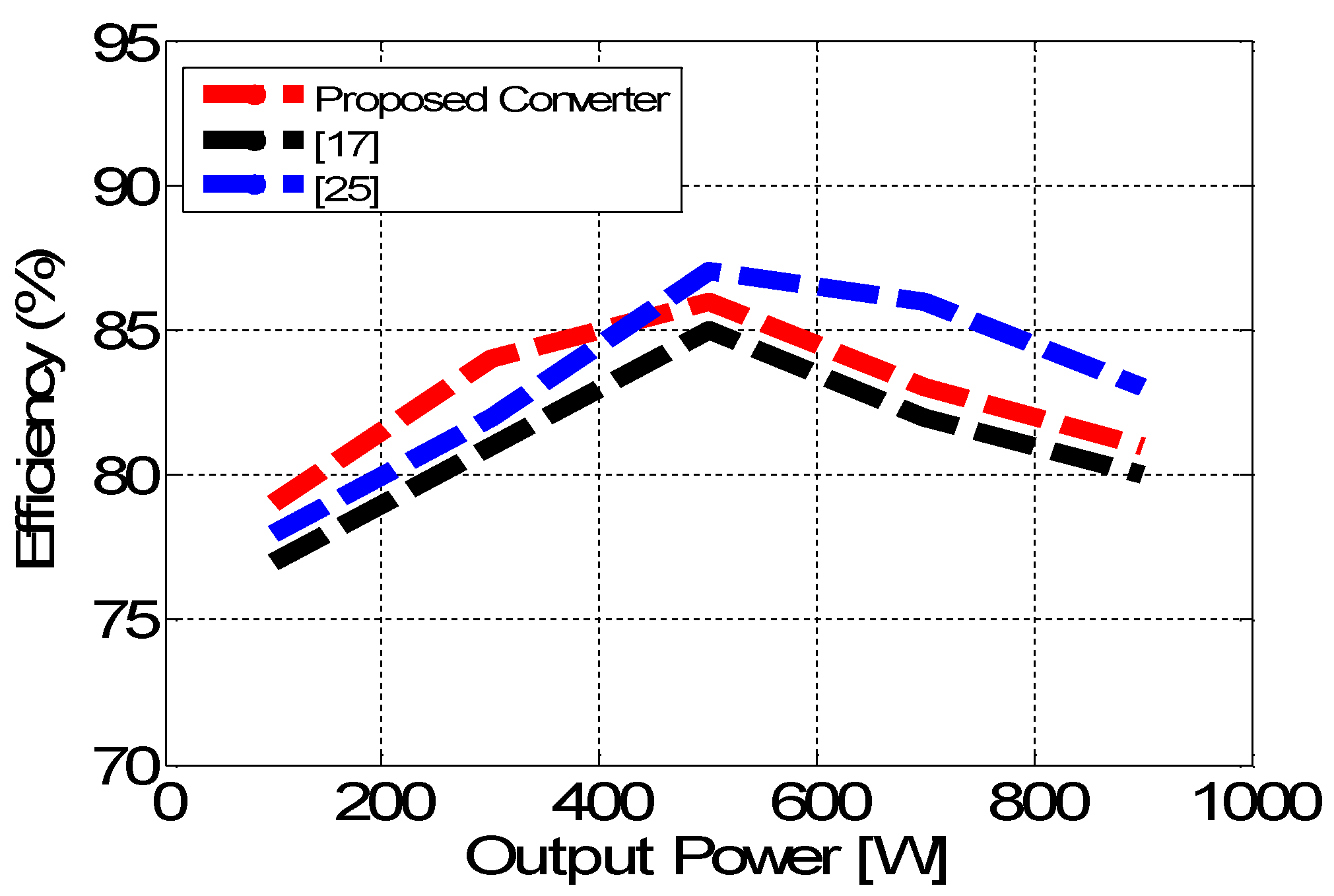
9. Efficiency Analysis

The major power losses of the proposed converter come from the magnetic losses, semiconductors losses, and ESR of the capacitors. The magnetic losses include copper and core losses. Semiconductor loss itself comprises switching and conduction loss, which can increase the power losses. For the efficiency calculation, some assumptions are supposed as follows; the equivalent series resistance (ESR) of capacitors is 2 Ω. The parasitic resistance of the coupled inductors and the input inductor are 1 Ω. Additionally, the leakage inductance of the coupled transformer is 4 µH, and the ON resistances of the switches are 0.27 Ω.
Figure 24 compares the efficiency of the suggested converter with the topologies in [17,25]. It can be seen that in D = 0.1, the proposed converter operates with higher efficiency for the output power range of 100–400 W. Figure 25 shows the power loss distribution of the suggested topology at PO = 375 W. Obviously, due to the exploited commutation strategy and using a smaller switching duty cycle, lower power loss comes from the bidirectional switches [29,30]. While in the existing topologies, semiconductors have a higher power loss rate.

10. Conclusions

In this study, a single-phase direct AC-AC converter has been introduced. The proposed converter can operate in buck-boost mode with a high voltage buck and boost ability. A trans-inverse coupled transformer has been exploited to attain high output voltage with a low switching duty cycle in boost in-phase mode. Unlike conventional single-phase AC -source converter, the proposed topology has a sinusoidal continuous input current with a low THD. Furthermore, the proposed converter shares the same ground between the output and input voltage, increasing the phase angle maintenance ability. To validate the performance of the proposed converter, it is simulated, and the impact of variations in each component in different operating points was investigated. Finally, a prototype of the proposed single-phase converter was implemented, and experimental tests were conducted to verify the operation of the circuit. The sufficiency of experimental results approved the theoretical design and simulations for both boost and buck states.

Author Contributions

All authors contributed equally to this work. All authors have read and agreed to the published version of the manuscript.

Funding

This research received no external funding.

Institutional Review Board Statement

Not applicable.

Informed Consent Statement

Not applicable.

Data Availability Statement

Not applicable.

Conflicts of Interest

The authors declare no conflict of interest.

References

  1. Moghassemi, A.; Padmanaban, S. Dynamic Voltage Restorer (DVR): A Comprehensive Review of Topologies, Power Converters, Control Methods, and Modified Configurations. Energies 2020, 13, 4152. [Google Scholar] [CrossRef]
  2. Liu, Y.; Sun, Y.; Su, M.; Li, X.; Ning, S. A Single Phase AC/DC/AC Converter with Unified Ripple Power Decoupling. IEEE Trans. Power Electron. 2017, 33, 3204–3217. [Google Scholar] [CrossRef]
  3. De Freitas, N.B.; Jacobina, C.B.; Gehrke, B.S.; Cunha, M.F. Transformer-Based Single-Phase AC–DC–AC Topology for Grid Issues Mitigation. IEEE Trans. Ind. Appl. 2019, 55, 4001–4011. [Google Scholar] [CrossRef]
  4. Felinto, A.S.; Jacobina, C.B.; Fabricio, E.L.L.; de Lacerda, R.P. Six-Leg Three-Phase AC–DC–AC Converter with Shared Legs. IEEE Trans. Ind. Appl. 2021, 57, 5227–5238. [Google Scholar] [CrossRef]
  5. Ashraf, N.; Abbas, G.; Ullah, N.; Al-Ahmadi, A.A.; Yasin, A.R.; Awan, A.B.; Jamil, M. A Transformerless AC-AC Converter with Improved Power Quality Employed to Step-Down Power Frequency at Output. Energies 2022, 15, 667. [Google Scholar] [CrossRef]
  6. Vijayagopal, M.; Zanchetta, P.; Empringham, L.; De Lillo, L.; Tarisciotti, L.; Wheeler, P. Control of a Direct Matrix Converter with Modulated Model-Predictive Control. IEEE Trans. Ind. Appl. 2017, 53, 2342–2349. [Google Scholar] [CrossRef]
  7. Maroti, P.K.; Esmaeili, S.; Iqbal, A.; Meraj, M. High step-up single switch quadratic modified SEPIC converter for DC microgrid applications. IET Power Electron. 2020, 13, 3717–3726. [Google Scholar] [CrossRef]
  8. Esmaeili, S.; Mahmoudi, A.; Kahourzadeh, S.; Mostaan, A. Dual winding magnetically coupled impedance-source inverters with Dc-rail voltage clamping circuits. In Proceedings of the 2021 IEEE 12th Energy Conversion Congress & Exposition-Asia (ECCE-Asia), Singapore, 24–27 May 2021. [Google Scholar]
  9. Esmaeili, S.; Karimi, S.; Siadatan, A.; Afjei, E.; Iqbal, A. Tapped switched-coupled-inductors Γ-source inverter. In Proceedings of the 2019 10th International Power Electronics, Drive Systems and Technologies Conference (PEDSTC), Shiraz, Iran, 12–14 February 2019. [Google Scholar]
  10. Esmaeili, S.; Iqbal, A.; Padmanaban, S.; Maroti, P.K.; Samiullah, M.; Lam, J. Asymmetrical switched inductor embedded impedance source inverters with reduced number of components. In Proceedings of the 2020 IEEE International Conference on Power Electronics, Drives and Energy Systems (PEDES), Jaipur, India, 16–19 December 2020. [Google Scholar]
  11. Guo, M.; Liu, Y.; Ge, B.; Abu-Rub, H. Optimum Boost Control of Quasi-Z Source Indirect Matrix Converter. IEEE Trans. Ind. Electron. 2018, 65, 8393–8404. [Google Scholar] [CrossRef]
  12. Bozorgi, A.M.; Hakemi, A.; Farasat, M.; Monfared, M. Modulation techniques for common-mode voltage reduction in the Z-source ultra-sparse matrix converters. IEEE Trans. Power Electron. 2019, 34, 958–970. [Google Scholar] [CrossRef]
  13. Fang, X.P.; Qian, Z.M.; Peng, F.Z. Single-phase Z-source PWM ACAC converters. IEEE Power Electron. Lett. 2005, 3, 121–124. [Google Scholar] [CrossRef]
  14. Tang, Y.; Xie, S.J.; Zhang, C.H. Z-source AC-AC converters solving commutation problem. IEEE Trans. Power Electron. 2007, 22, 2146–2154. [Google Scholar] [CrossRef]
  15. Nguyen, M.K.; Jung, Y.G.; Lim, Y.C. Single-phase AC-AC converter based on quasi-Z-source topology. IEEE Trans. Power Electron. 2010, 25, 2200–2210. [Google Scholar] [CrossRef]
  16. Nguyen, M.-K.; Lim, Y.C.; Kim, Y.-J. A Modified Single-Phase Quasi-Z-Source AC–AC Converter. IEEE Trans. Power Electron. 2011, 27, 201–210. [Google Scholar] [CrossRef]
  17. Banaei, M.R.; Ahrabi, R.; Elmi, M. Single-phase safe commutation trans-Z-source AC-AC converter. IET Power Electron. 2015, 8, 190–201. [Google Scholar] [CrossRef]
  18. Banaei, M.R.; Alizadeh, R.; Jahanyari, N.; Najmi, E.S. An ac Z-source converter based on gamma structure with safe-commutation strategy. IEEE Trans. Power Electron. 2016, 31, 1255–1262. [Google Scholar] [CrossRef]
  19. Aleem, Z.; Yang, H.-K.; Ahmed, H.F.; Winberg, S.L.; Park, J.-W. A Class of Single-Phase Z-Source AC–AC Converters with Magnetic Coupling and Safe-Commutation Strategy. IEEE Trans. Ind. Electron. 2021, 68, 8104–8115. [Google Scholar] [CrossRef]
  20. Sharifi, S.; Monfared, M. Modified Series and Tapped Switched-Coupled-Inductors Quasi-Z-Source Networks. IEEE Trans. Ind. Electron. 2019, 66, 5970–5978. [Google Scholar] [CrossRef]
  21. Reddivari, R.; Jena, D. A Negative Embedded Deferential Mode Γ -Source Inverter with Reduced Switching Spikes. IEEE Trans. Circuits Syst. 2020, 7, 2009–2013. [Google Scholar]
  22. Liu, H.; Zhou, B.; Li, Y. High-Efficiency T-Source Inverter with Low Voltage Spikes across the Switch Bridge. IEEE Trans. Power Electron. 2020, 35, 10554–10566. [Google Scholar] [CrossRef]
  23. Ahmed, H.F.; Cha, H. A New Class of Single-Phase High-Frequency Isolated Z-Source AC–AC Converters with Reduced Passive Components. IEEE Trans. Power Electron. 2018, 33, 1410–1419. [Google Scholar] [CrossRef]
  24. Ahmed, H.F.; El Moursi, M.S.; Irshad, T.; El-Saadany, E. Family of single-phase isolated high-frequency transformer integrated improved magnetically coupled Z-source AC–AC converters. IET Power Electron. 2020, 13, 1901–1910. [Google Scholar] [CrossRef]
  25. He, L.Z.; Nai, J.X.; Zhang, J.H. Single-phase safe-commutation trans-z-source AC-AC converter with continuous input current. IEEE Trans. Ind. Electron. 2018, 65, 5135–5145. [Google Scholar] [CrossRef]
  26. Esmaeili, S.; Siadatan, A.; Jahromi, A.Z.; Shirazi, P. A filterless single-phase AC-AC converter based on coupled inductors with safe commutation strategy and continuous input current. In Proceedings of the IEEE International Conference on Industrial Technology (ICIT), Toronto, ON, Canada, 22–25 March 2017; pp. 12–17. [Google Scholar]
  27. Mousavi, S.M.J.; Babaei, E.; Alizadeh, D.; Komurcugil, H. Single-phase AC-AC Z-source converter based on asymmetrical gamma structure with continuous input current and safe commutation strategy. IET Power Electron. 2021, 14, 680–689. [Google Scholar] [CrossRef]
  28. Esmaeili, S.; Mahmoudi, A.; Kahourzadeh, S. Sinusoidal input current single-phase AC-AC converter based on coupled transformer with reduced turns ratio. In Proceedings of the IEEE 12th Energy Conversion Congress & Exposition-Asia (ECCE-Asia), Singapore, 24–27 May 2021. [Google Scholar]
  29. Azimi, E.; Khodaparast, A.; Rostami, M.J.; Adabi, J.; Adabi, M.E.; Rezanejad, M.; Rodrigues, E.M.G.; Pouresmaeil, E. X-Type Step-Up Multi-Level Inverter with Reduced Component Count Based on Switched-Capacitor Concept. Electronics 2020, 9, 1987. [Google Scholar] [CrossRef]
  30. Khodaparast, A.; Azimi, E.; Azimi, A.; Adabi, M.E.; Adabi, J.; Pouresmaeil, E. A New Modular Multilevel Inverter Based on Step-Up Switched-Capacitor Modules. Energies 2019, 12, 524. [Google Scholar] [CrossRef] [Green Version]
Figure 1. Schematic of the single-phase AC-AC Trans Z-source converter [17].
Energies 15 04319 g001
Figure 2. Schematic of the single-phase AC-AC Γ -source converter [18].
Energies 15 04319 g002
Figure 3. Trans-inverse magnetic coupling single-phase AC-AC converter.
Energies 15 04319 g003
Figure 4. Switching signals of safe commutation approach in (a) boost in-phase mode and (b) buck/boost out-of-phase mode.
Energies 15 04319 g004
Figure 5. Operation intervals of the introduced topology for boost in-phase state when Vi > 0, (a): non-shoot-through state, (b): commutation state if Ii + ILkIlf > 0, (c): commutation mode when Ii + IlkIlf < 0 and ILk = ILm, (d): commutation state if Ii + Ilk-Ilf < 0 and ILk − ILm < 0, (e): shoot-through state.
Energies 15 04319 g005aEnergies 15 04319 g005b
Figure 6. Operation intervals of the introduced topology for boost in-phase mode when Vi < 0, (a): non-shoot-through state, (b): commutation state if Ii + IlkIlf < 0, (c): commutation state if Ii + ILkIlf > 0 and ILk = ILm, (d): commutation state if Ii + IlkIlf > 0 and ILkILm > 0, (e): shoot-through state.
Energies 15 04319 g006aEnergies 15 04319 g006b
Figure 7. Equivalent circuits of the suggested topology: (a) NST state and (b) ST state.
Energies 15 04319 g007
Figure 8. Output voltage gain versus duty cycle with different turns ratio.
Energies 15 04319 g008
Figure 9. Dynamic voltage restorer based on the proposed converter.
Energies 15 04319 g009
Figure 10. Output voltage gain verse the duty cycle for the introduced topology, topology [17], and topology [18], with the same turns ratio (n = 1.5).
Energies 15 04319 g010
Figure 11. Simulation results of the boost in-phase mode with n = 1.5, R = 30 Ω, and D = 0.1. (a) output filter and input current; (b) Voltage across C1; (c) voltage across C2; (d) output and input voltages; (e) voltage across S1; (f) voltage across S2.
Energies 15 04319 g011
Figure 12. Simulation results of the boost in-phase mode with n = 1.4, R = 30 Ω, and D = 0.1. (a) output filter and input current; (b) Voltage across C1; (c) voltage across C2; (d) output and input voltages; (e) voltage across S1; (f) voltage across S2.
Energies 15 04319 g012
Figure 13. Simulation results of the proposed converter in boost in-phase mode with n = 1.5, R = 30 Ω, and D = 0.12. (a) output filter and input current; (b) Voltage across C1; (c) voltage across C2; (d) output and input voltages; (e) voltage across S1; (f) voltage across S2.
Energies 15 04319 g013
Figure 14. Simulation results of the buck out-of-phase mode with n = 2, R = 2 Ω and D = 0.8. (a) output filter and input current; (b) Voltage across C1; (c) voltage across C2; (d) output and input voltages; (e) voltage across S1; (f) voltage across S2.
Energies 15 04319 g014
Figure 15. Simulation results of the proposed DVR at 60% voltage sag compensation: (a) line voltage, (b) output voltage of the converter, (c) load voltage.
Energies 15 04319 g015aEnergies 15 04319 g015b
Figure 16. Simulation results of the proposed DVR at 25% voltage swell compensation: (a) line voltage, (b) output voltage of the converter, (c) load voltage.
Energies 15 04319 g016
Figure 17. The overview of the implemented test setup.
Energies 15 04319 g017
Figure 18. The experimental results of the proposed single-phased topology for Boost-in-phase operating mode: (a) input and output voltage waveforms, (b) capacitors’ voltages, (c) voltages of the power switches, and (d) input and output current waveforms.
Energies 15 04319 g018
Figure 19. The experimental results of the proposed topology for Buck out-of-phase operating mode: (a) input and output voltage waveforms, (b) input and output current waveforms, (c) voltage stresses over power switches, and (d) capacitors’ voltages.
Energies 15 04319 g019
Figure 20. Simulation waveforms of the input current for: (a) boost in-phase operating mode in the proposed converter, (b) buck out-of-phase operating mode in the proposed converter, (c) boost in-phase operating mode in the conventional AC Γ-source converter [18], (d) buck out-of-phase operating mode in the conventional AC Γ-source converter [18].
Energies 15 04319 g020aEnergies 15 04319 g020b
Figure 21. Simulation input current spectrums of the proposed topology in [18] for: (a) boost in-phase operating mode when D = 0.1, (b) buck out-of-phase operating mode when D = 0.78.
Energies 15 04319 g021
Figure 22. Simulation spectrums of the proposed topology for the boost in-phase operating mode when D = 0.1: (a) output voltage, (b) input current.
Energies 15 04319 g022
Figure 23. Simulation spectrums of the proposed topology for the buck out-of-phase operating mode when D = 0.78: (a) output voltage, (b) input current.
Energies 15 04319 g023
Figure 24. Measured efficiency of the proposed converter and converters in [17,25] with D = 0.1.
Energies 15 04319 g024
Figure 25. Power loss distribution in the suggested converter at PO = 375 W.
Energies 15 04319 g025
Table 1. Comparison of the proposed converter and the similar topologies.
Parameter[13][15][16][17][18][25]Proposed
Converter
V o V i 1 D 1 2 D 1 D 1 2 D 1 D 1 2 D 1 D 1 ( n + 2 ) D 1 D 1 ( 1 + 1 n + 1 ) D 1 1 ( n + 2 ) D ( 1 D ) ( n 1 ) n 1 2 n D + D
Ii P o V i 1 D P o V i P o V i P o V i d P o V i ( 1 D ) P o V i P o V i
V C 1 V i 1 D 1 2 D 1 D 1 2 D 1 D 1 2 D ( n + 1 ) D 1 ( n + 2 ) D 1 D 1 ( 1 + 1 n + 1 ) D ( n + 1 ) D 1 ( n + 2 ) D ( 1 D ) ( n 1 ) n 1 2 n D + D
V C 2 V i 1 D 1 2 D 1 D 1 2 D 1 D 1 2 D 1 D 1 ( n + 2 ) D - 1 D 1 ( n + 2 ) D n D n 1 2 n D + D
IL1 P o V i P o V i P o V i P o V i - P o V i P o V i
IL2 P o V i P o V i ( 1 D ) P o d V i ----
Num. of capacitors3323233
Num. of inductors + coupled transformer3 + 03 + 02 + 02 + 11 + 11 + 12 + 1
Num. of switches2444464
Total num. of components81081081110
Table 2. Test system properties.
ParametersValues
Maximum input voltage (Vi)100 V
input voltage frequency (fin)50 Hz
switching frequency (fsw)20 kHz
DSPTMS320F28335
Load (R)30 Ω and 2 Ω
Power switch (MOSFET)IRFP460
C110 µF
C210 µF
L1 mH
Lf1.2 mH
Cf47 µF
LM820 µH
Table 3. THD ii in the proposed converter and Γ SC in [18].
THD ii Γ SC in [18] Proposed Converter
Boost in-phase mode (D = 0.1)50.77%5.86%
Buck out-of-phase mode (D = 0.78)136.72%8.94%
Table 4. THD vo in the proposed converter.
THD voProposed Converter
Boost in-phase mode (D = 0.1)2.35%
Buck out-of-phase mode (D = 0.78)3.83%
Publisher’s Note: MDPI stays neutral with regard to jurisdictional claims in published maps and institutional affiliations.

