1. Introduction
Power electronics converters play a major role in numerous critical applications, causing internal converter faults to carry significant consequences. Internal faults can disrupt or even interrupt critical processes, bringing severe economic losses, service unavailability, safety risks, or even loss of life. Therefore, power converter reliability and system resilience have become extremely important over the last years. Fault tolerance provides a way to mitigate the effects of internal converter faults, allowing the system to remain in operation until the faults are repaired. This significantly reduces the impact of faults and dramatically increases the system’s resilience, avoiding undesired downtime. Semiconductor faults are one of the main causes of converter failure, so the development of fault-tolerant techniques to mitigate semiconductor faults is critical.
An Uninterruptible Power Supply (UPS) provides protection to a critical load, improving its resilience. Hence, it is imperative to guarantee that the load is protected not only against grid faults but also from internal faults in the UPS system itself. Therefore, fault-tolerant strategies are crucial to reduce or eliminate the effect of internal UPS faults, allowing the UPS and, consequently, the critical load to remain in operation after a fault occurs. This is particularly important in double-conversion UPS systems since all power supplied to the load flows permanently through the power converters.
Multilevel converters are now largely used in high-power and high-voltage industrial applications, including UPS systems, presenting significant advantages over conventional 2-level converters, such as improved power quality, lower switching losses and lower semiconductor voltage stress [
1]. Neutral-Point-Clamped (NPC) converters represent one of the most widely used multilevel topologies in industrial systems [
1].
Several fault-tolerant approaches have been proposed to correct semiconductor faults in power electronics converters over the years [
2,
3,
4,
5,
6,
7,
8,
9]. These approaches can be classified into two fundamental types: redundant and non-redundant. Redundant techniques typically include redundant equipment, which can substitute any damaged part(s). Redundant topologies can have three types of redundancy: switch-level, phase-level, and converter-level redundancy. In switch-level redundancy, additional switches are typically installed in series or parallel with the base topology switches to ensure converter operation when one of the switches fails [
2,
4]. In phase-level redundancy, an additional converter leg is added, which can replace the faulty leg entirely or complement its operation. The redundant leg may display the same configuration as the main legs [
9,
10,
11,
12,
13], effectively substituting the faulty one in post-fault operation, or a distinct topology [
14,
15,
16,
17,
18,
19,
20], which may provide advantages in regular operation but does not entirely replace the faulty phase after the fault. Converter-level redundancy consists of the association of several identical converters, which can continue to operate even if one (or more) of them fails. This approach is often used in high-power UPS systems, which adopt a modular structure with several converters installed in parallel. By installing surplus converter modules, fault tolerance is obtained. When a converter fails, the UPS can continue operating normally, as long as the remaining modules can supply enough power to the load. With this approach, reliability increases with the number of surplus power modules, but so does the cost. This solution can be costly and is only viable to protect highly critical loads, such as high-tier datacenters.
Non-redundant fault tolerance techniques do not use redundant hardware and typically present significantly lower costs. On the other hand, a complete correction of the fault is not always possible. This type of approach can be based solely on software adaptations, relying only on changes to the control and modulation strategies [
21,
22,
23,
24,
25,
26,
27,
28,
29,
30], or require some changes to the converter topology [
29,
30,
31,
32,
33,
34,
35,
36,
37,
38,
39,
40,
41,
42,
43,
44,
45,
46,
47,
48,
49,
50,
51,
52,
53,
54,
55,
56,
57,
58,
59,
60,
61,
62,
63,
64,
65,
66,
67]. Software-based fault correction presents the lowest possible complexity and cost but typically carries significant operational limitations, resulting in reduced post-fault performance. This type of approach cannot correct the loss of available switching states and therefore presents a limited correction potential. Nonetheless, these techniques have the advantage of requiring no hardware changes, which means they can be implemented in any system.
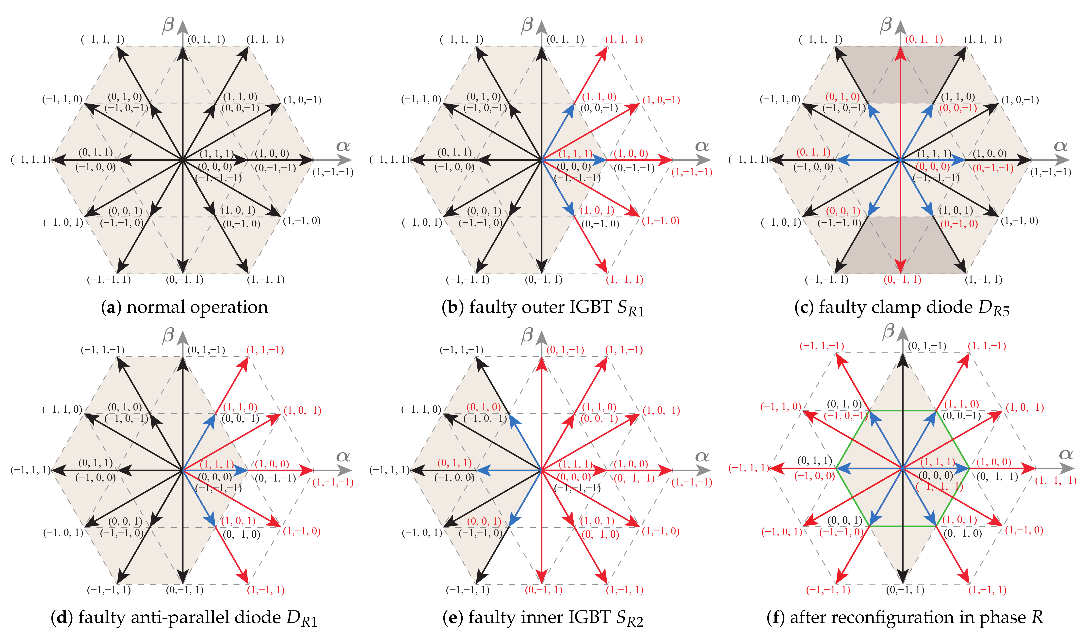
In NPC converters, the inherent voltage vector redundancy allows a greater degree of control when in the presence of a fault, in comparison to 2-level converters. Hence, several solutions have been proposed to alter the control and modulation stages to correct IGBT faults in PWM-based AC/DC converters [
22,
23,
24,
25,
26,
27,
29]. In AC/DC applications, the IGBTs have a reduced use compared to the diodes, which allows these techniques to acceptably correct outer IGBT faults [
22,
23]. In the case of inner IGBT faults, the effect of the fault can only be attenuated [
23,
24,
25] since a large number of switching states is lost. In DC/AC applications, IGBT faults have a more severe impact on the NPC converter and cannot be fully corrected without topology changes, causing a derating [
30].
NPC clamp diode faults can also be corrected through controller adaptations, as proposed in [
28]. In that solution, clamp diode faults are corrected by altering the PWM patterns to inhibit the use of switching states that use the affected diode. However, this correction is only valid for this type of fault.
Most proposed solutions for controller and modulation adaptations in post-fault operation completely eliminate the switching states affected by the fault from the switching possibilities or modulation patterns.
Given the limited corrective potential of fault-tolerant schemes based solely on controller and modulation changes, several topology changes have been proposed to improve non-redundant fault-tolerant performance. Several topology changes have been proposed for NPC converters. One of the NPC-derived topologies is the Active NPC topology [
32,
33,
34,
35,
36], which achieves increased control state redundancy by adding 2 IGBTs in the clamping circuit.
Other topologies adopt minor changes to the standard NPC configuration, adding only slow switches, such as triacs or solid-state relays (SSR), to increase the fault-tolerant capabilities of the converter without significantly increasing the cost of the system. One of the most common non-redundant solutions is the permanent connection of the AC terminal of the faulty phase to the midpoint of the DC bus. This solution requires only one additional bidirectional switch per phase, making it a very cost-effective solution. This solution has been widely used in both 2-level [
37,
38,
40,
41,
42,
43,
44,
45,
46,
63,
64,
65,
66] and NPC [
29,
30,
31,
47,
48,
49,
50,
51,
52,
53,
54,
55] converters. A similar approach has been proposed for 2-level converters in [
61,
62], connecting the faulty phase to an auxiliary capacitor instead of the DC bus midpoint. In [
67], 2 additional switches are used to bypass the inner IGBTs when faulty. With these approaches, the controller can only operate normally with modulation indexes below 0.5, which implies a derating of the system. Even though a derating may be acceptable in some applications [
30], such as motor drives [
37,
40,
51,
54,
67] or generation [
38,
46,
47,
53,
63,
64], it is not viable in UPS applications since the system cannot compromise or restrict the operation of the protected critical load.
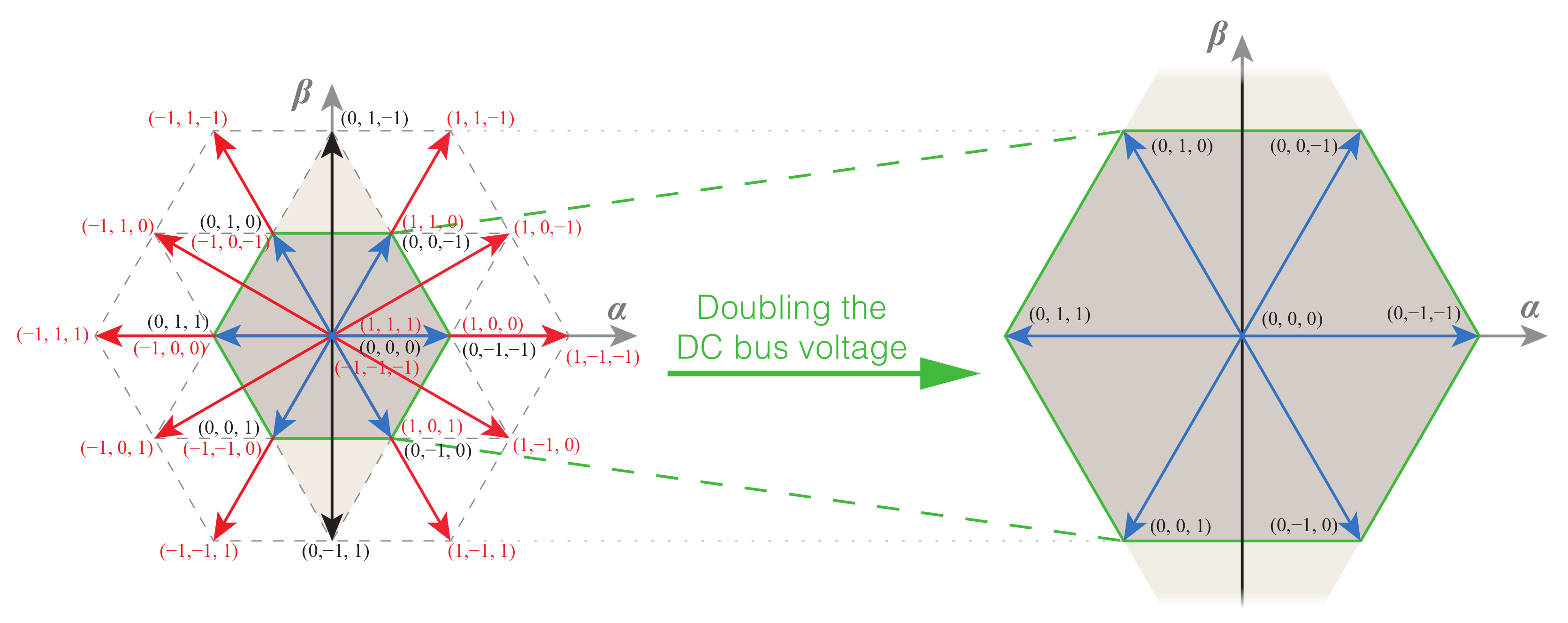
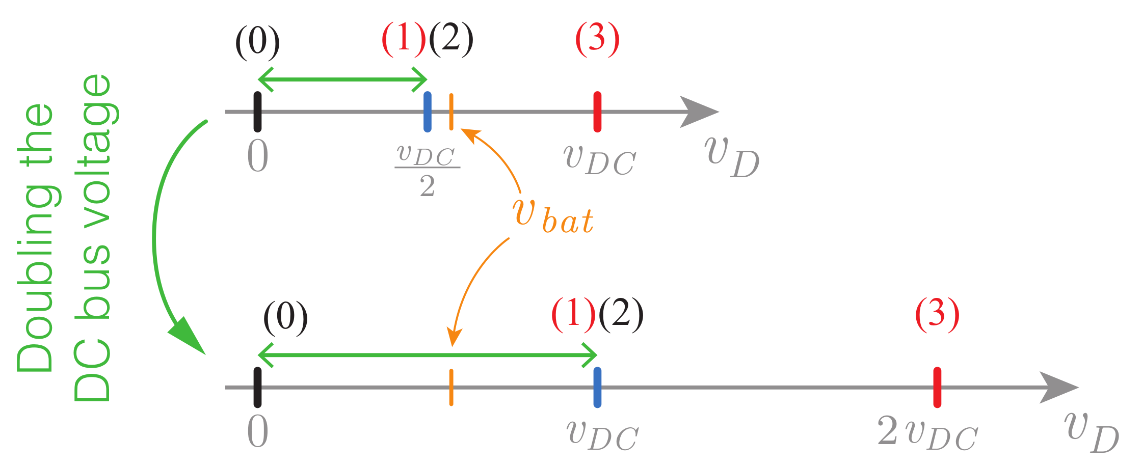
One solution proposed to avoid a post-fault derating of the converter is to increase the DC bus voltage after the fault [
31,
48,
49,
50,
61,
65]. This ensures that the initial modulation area is kept in post-fault scenarios, enabling the system to retain full-rated capacity. On the other hand, this implies that all power switches and capacitors need to have a higher voltage rating.
Some solutions have also been proposed based on the connection of the DC bus midpoint to the neutral point of the machine (in machine drives) or power supply (when available) [
37,
38,
39].
In back-to-back systems, another possible solution is the sharing of a converter leg between the two converters to improve the post-fault performance of the system [
40,
56,
57,
58,
59,
60]. This effectively reduces the back-to-back converters to a 5-leg configuration but allows acceptable performance after a fault occurs. This strategy does, however, increase the dependency between the two converters in the back-to-back configuration. In the case of a UPS, this could compromise the protection of the load from phenomena in the grid.
In the last years, Model Predictive Control (MPC) has received extensive attention from the research community and has proven to be an excellent control solution for power electronics converters [
68,
69,
70,
71,
72,
73]. In particular, Finite-Control-Set MPC (FCS-MPC) has become extremely popular in power electronics applications, leveraging the discrete nature of power converters to formulate an intuitive control algorithm, without requiring a modulator.
FCS-MPC presents several important advantages, such as its fast dynamic response, intuitive formulation, easy inclusion of non-linearities and operation constraints and simultaneous control of multiple variables in a single control loop [
70]. The ability to control multiple variables simultaneously makes FCS-MPC highly advantageous in systems with multiple concurrent objectives, since it does not require the tuning of several interdependent control loops. FCS-MPC is also advantageous for multi-converter systems, since the controller(s) can consider the cumulative impact of several converters, promoting improved cooperation and system performance [
74].
Another major advantage of FCS-MPC is its versatility. The ability to easily include non-linearities and system constraints allows a direct application to complex systems for which a conventional controller would be very hard to design. The ability to include advanced control restrictions presents great potential for fault-tolerant applications. The techniques proposed in this paper take advantage of this to implement a selective switching state exclusion from the available control set.
Despite its advantages, FCS-MPC still presents some important challenges [
68,
69,
70,
71,
72]. Weighting factor selection is typically a lengthy and complex procedure, which optimizes converter performance in specific operating conditions—often compromising performance in other operating points or the dynamic response [
75,
76,
77]. To tackle this problem, several techniques have been proposed to automatically adjust weighting factors during operation [
77,
78,
79,
80]. In particular, the solution proposed in [
77] provides a continuous weighting factor adjustment, allowing the controller to adapt to different operating conditions and improving both steady-state performance and the dynamic response. Due to its high adaptability to different conditions, this technique presents great potential for fault-tolerant applications, since it can adapt to new (and initially unforeseen) operating conditions without re-tuning.
A cooperative FCS-MPC principle is proposed in [
74], to improve multi-converter performance without increasing the overall computational load of the system (compared to independent controllers). This cooperative solution is combined with the dynamically weighted FCS-MPC technique proposed in [
77] and applied to a 3-level double conversion UPS system. The resulting control system proposed in [
74] is highly adaptable and promotes high cooperation between all converters of the UPS, improving the overall performance and dynamic response.
Other FCS-MPC solutions have also been proposed for UPS applications. For example, in [
81,
82,
83,
84,
85] FCS-MPC solutions are proposed for 2-level UPS inverters. However, all these solutions focus uniquely on the inverter stage of the UPS and overlook the remaining system. Other studies focus on the parallel connection of multiple UPS inverters using FCS-MPC techniques [
86,
87]. Once again, these techniques focus only on the inverter stage of the UPS and a 2-level topology is used. In [
74] a full 3-level UPS system is studied, considering all UPS converters (rectifier, inverter and DC-DC) and all operation modes. In [
87,
88] FCS-MPC techniques are proposed to control full UPS modules (rectifier+inverter) connected in parallel. These studies use both 2-level [
87] and 3-level [
88] topologies. However, the DC-DC converter and UPS battery bank are overlooked. Thus the operation of a full UPS system using FCS-MPC was rarely studied, especially with multilevel topologies. In addition, most solutions in the literature use conventional fixed weighting factor approaches, which may not provide sufficient adaptability to enable post-fault operation without altering controller parameters.
Due to the dynamic nature of the controller proposed in [
74], this technique should be particularly suited for use in fault-tolerant UPS systems, since it can dynamically adapt to different operating conditions without changes to the controller parameters. The cooperative principle used between the converters of the UPS is also advantageous, since it allows each converter to aid in compensating the limitations imposed by faults in the others only when needed (without compromising normal operation). Even though [
74] demonstrated the advantages of this controller, it did not study the system response in case of faults and did not propose any mechanisms to allow post-fault operation. Thus, this paper uses the control system proposed in [
74], now proposing several control adaptations, topology changes and additional techniques to create a highly resilient non-redundant fault-tolerant UPS system.
Some solutions have previously been presented featuring fault-tolerant measures to correct IGBT open-circuit (OC) faults in FCS-MPC-based systems. The studies in [
41,
42,
43,
44,
45] correct OC faults in 2-level grid-connected converters by connecting the faulty phase to the midpoint of the DC bus using additional switches. A similar approach is taken in [
61], where the faulty phase is connected to an auxiliary capacitor charged at half the DC bus voltage. In these cases, the prediction model is altered in order to consider the correct post-fault output voltage in the faulty phase. In [
41,
44] an additional objective is included in the cost function, to maintain DC bus capacitor balance in post-fault conditions. In [
44] the system can operate even with a phase current sensor fault. In [
45] the objective function is altered to minimize post-fault power ripple. In [
43], a multi-vector approach is taken, applying multiple voltage vectors in each sampling period. Thus, in fault-tolerant operation the controller presents a modulator-like output. All solutions mentioned above require a distinct control-set and altered prediction model to be used after the fault.
In [
47], a fault-tolerant FCS-MPC controller is proposed for doubly-fed induction generator applications, using 3-level NPC converters. As in the previous cases, slow switches are used to connect the faulty-phase to the midpoint of the DC bus, in all cases of IGBT OC fault in the NPC converter (regardless of the faulty switch). After the reconfiguration, the controller permanently considers a fixed switching state in the faulty phase (equivalent to the reconfiguration), thus reducing the available control set. The technique in [
47] can also correct short-circuit faults, by permanently removing the switching states that cause a short-circuit from the control-set. In both cases, the post-fault control-set is merely a subset of the one available in normal conditions instead of a distinct one, making controller implementation significantly simpler. The solutions in [
27,
31] provide fault-tolerant capabilities to 3-level NPC rectifiers and motor drive inverters and also consider a subset of the initial control set for fault-tolerant operation. In these cases, switching states affected by the fault are excluded from the control set only when current in the faulty phase flows in a specific direction (affected by the fault), which allows the converter to still use them in other conditions. However, these studies do not explain how this exclusion is implemented. Moreover, [
27] considers only faults in inner IGBTs of the NPC converter (all other faults are overlooked) and, since no other corrective actions are taken, the converter is actually unable to correct the effect of these faults (it is somewhat reduced, but high current distortion still exists). In [
31] both inner and outer IGBT faults can be corrected. In the case of inner IGBTs, the faulty phase is connected to the DC bus midpoint using additional switches. To avoid derating, the DC bus voltage is increased in post-fault conditions. However, the new DC bus voltage value is chosen manually, so it cannot automatically adapt to varying load conditions.
The previously described fault-tolerant FCS-MPC techniques study fault-tolerance in a single converter and imply a derating of the system in post-fault operation. Only the solution in [
61] avoids system derating, by doubling the DC bus voltage after a fault is detected (using an auxiliary boost converter which drives the DC bus of the inverter).
Despite the great versatility of FCS-MPC, its application to fault-tolerant solutions has been relatively limited, focusing mostly on the study of single-converter systems (most frequently of 2-level type) and correcting only IGBT faults. Moreover, few studies have leveraged the versatility of FCS-MPC to impose advanced switching constraints in fault-tolerant operation. Also, little to no studies have focused on fault-tolerant FCS-MPC UPS systems and most solutions consider a post-fault derating, which is unacceptable in UPS applications.
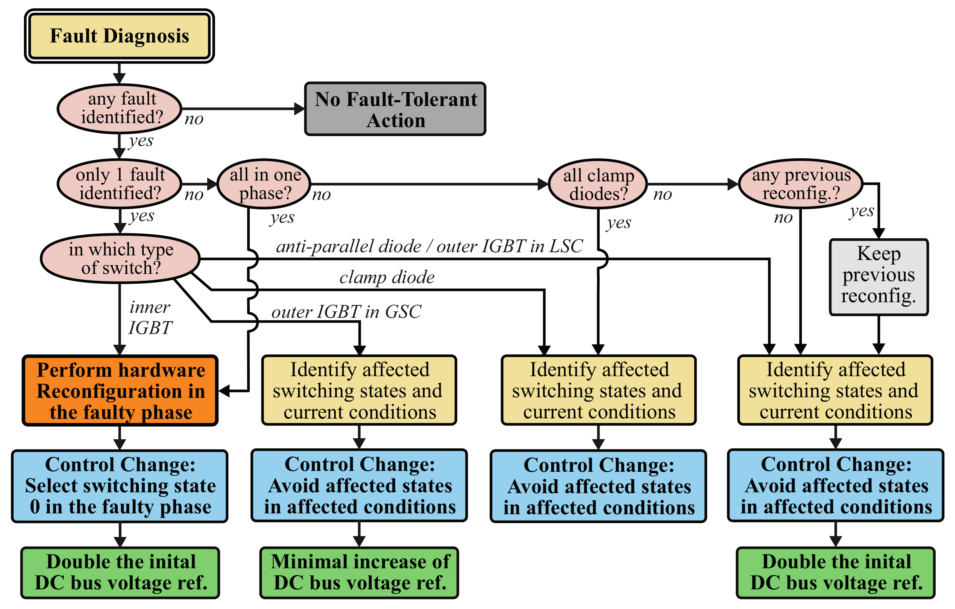
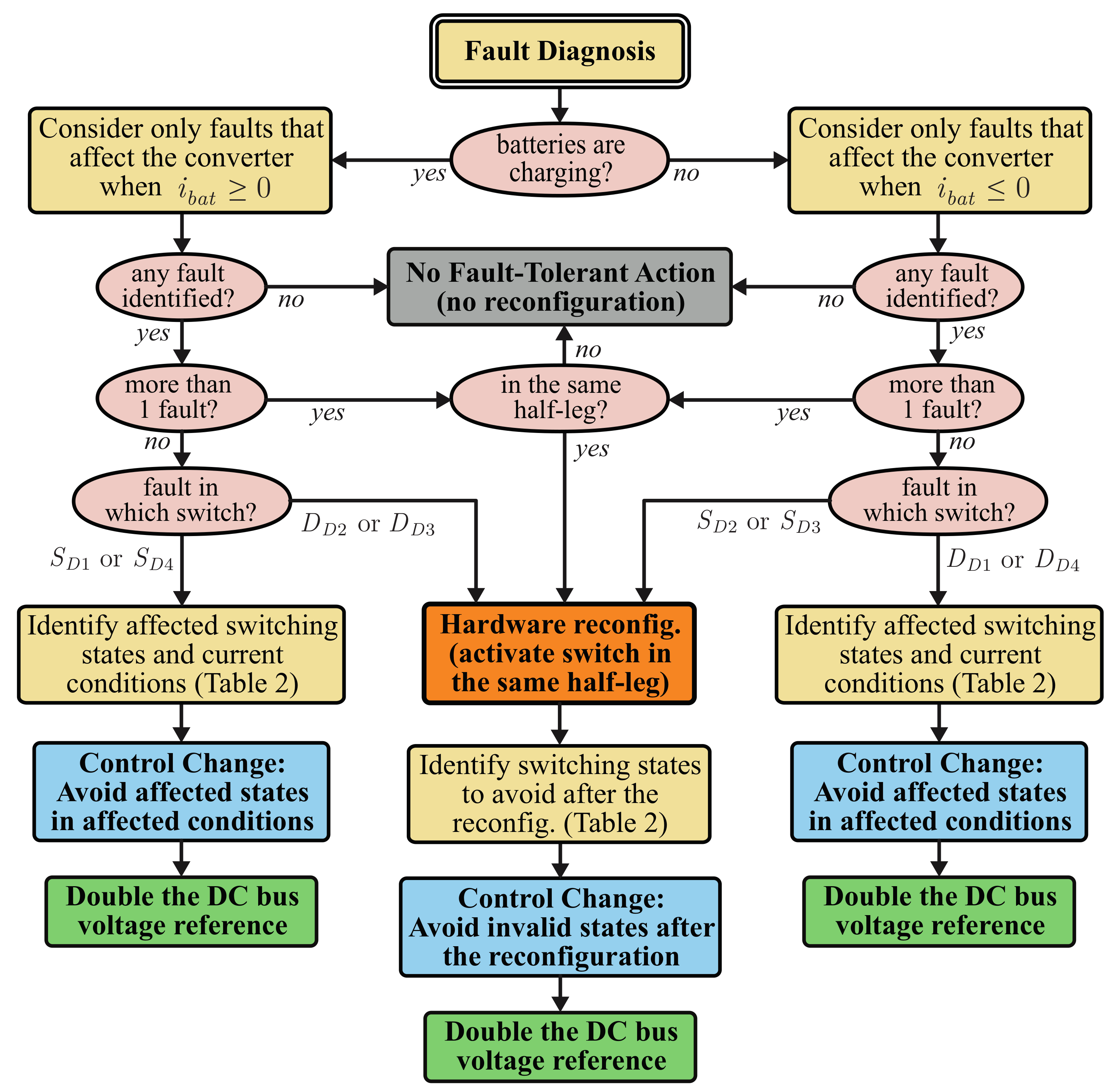
This paper proposes a new non-redundant fault-tolerant technique for a complete double-conversion UPS, based on multilevel topologies and leveraging the versatility of FCS-MPC. The proposed system uses two 3-level NPC converters and a 3-level DC-DC converter. A fault-tolerant scheme is proposed to correct faults in all UPS converters, guaranteeing full-rated operation after open-circuit faults in any semiconductor of the UPS. Unlike the solutions found in the literature, which focus mostly on the correction of OC faults in the IGBTs, the technique proposed in this paper can correct faults in all semiconductors of the UPS: IGBTs, clamping diodes, and anti-parallel diodes.
Even though numerous fault-tolerant solutions have been proposed for NPC converters, the fault-tolerant operation of a full multilevel-based double-conversion UPS system has not been properly studied. Also, little to no studies have approached fault tolerance in the 3-level DC-DC converter, especially when used in this kind of system. The proposed solution uses a common approach for all UPS converters, based on three types of corrective actions: controller adaptations, hardware reconfiguration, and DC bus voltage adjustment.
Unlike most previously proposed solutions, the technique proposed in this paper does not use the same corrective action for all types of faults. Instead, highly differentiated corrective actions are taken depending on the faulty semiconductor type and location. This minimizes the impact of the fault correction on the remaining converters and maximizes the overall UPS performance in post-fault conditions.
In addition, conversely to most fault-tolerant solutions found in the literature (FCS-MPC and modulator-based), the proposed technique does not entirely prevent the use of the switching states affected by the fault. Instead, a new technique is described in detail to selectively remove these switching states from the control-set only in affected current conditions. This means those switching states can still be used in all conditions that do not require the faulty component to carry a current. Thus, the converter retains higher control versatility. This type of advanced switching state exclusion is made possible by FCS-MPC and would be impossible to implement with most other control techniques.
The proposed solution requires minimal hardware expansion and allows full rated post-fault operation even after simultaneous faults in all UPS converters. The proposed technique can even correct multiple simultaneous faults in the same converter, depending on the faulty switches.
To summarize, this paper presents a detailed fault impact analysis and proposes a new, highly comprehensive, non-redundant fault-tolerant technique for multilevel-based UPS systems, which allows fast correction of OC faults in any semiconductor in the UPS (IGBTs or diodes) and full-rated post-fault operation. The proposed solution leverages the power and versatility of FCS-MPC to enable a selective switching state exclusion and implements highly differentiated corrective action for different faults, thus maximizing post-fault performance. The proposed technique can simultaneously correct faults in the 3 converters of the UPS and even several cases of multiple simultaneous faults within the same converter.
Experimental results are presented to demonstrate the performance and advantages of the proposed fault-tolerant solution in different scenarios.
This paper is organized as follows: in
Section 2, the studied UPS system is described.
Section 3 presents a detailed fault impact analysis on the modulation capabilities of the grid-side and load-side converters and the proposed fault-tolerant solutions for these converters are presented.
Section 4 presents a fault impact analysis on the DC-DC converter as well as the proposed fault-tolerant solution for this converter. In
Section 5, experimental results are presented and discussed. The advantages, shortcomings, and applicability of the proposed solution are discussed in detail in
Section 6.
2. System Description
In this paper, a 3-level double conversion UPS system is proposed, consisting of two 3-Level Neutral-Point-Clamped (3LNPC) converters and a 3-Level DC-DC (3LDC) converter sharing a single DC bus, as represented in
Figure 1.
The grid-side converter (GSC) is connected to the grid by an inductive filter, while the load-side converter (LSC) is connected to the load using an LC filter. The DC-DC converter (DCC) connects the DC bus to the battery bank using an inductive filter. In this paper, the 3 phases on the grid side are represented by while on the load side, they are represented by . The IGBTs on each leg are denoted as , where X denotes the phase and n identifies the IGBT, numbered from top (1) to bottom (4). The anti-parallel diodes are identified as , using the same numbering. The clamping diodes are denoted as and (numbered from top to bottom). The IGBTs and anti-parallel diodes of the 3LDC converter as denoted as and (numbered from top to bottom).
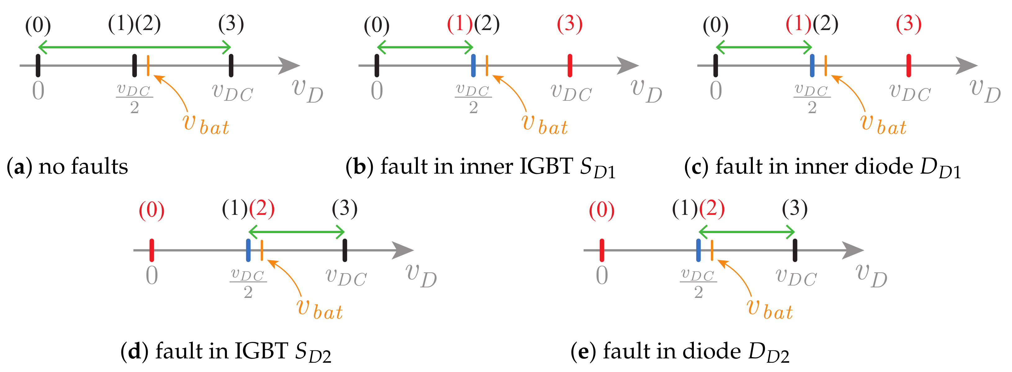
Each 3LNPC converter has 3 possible switching states in each phase X (), which activate different IGBT pairs and produce pole voltage values , respectively.
The 3LDC converter has 4 possible switching states, , which activate different IGBT pairs and produce voltage values , respectively.
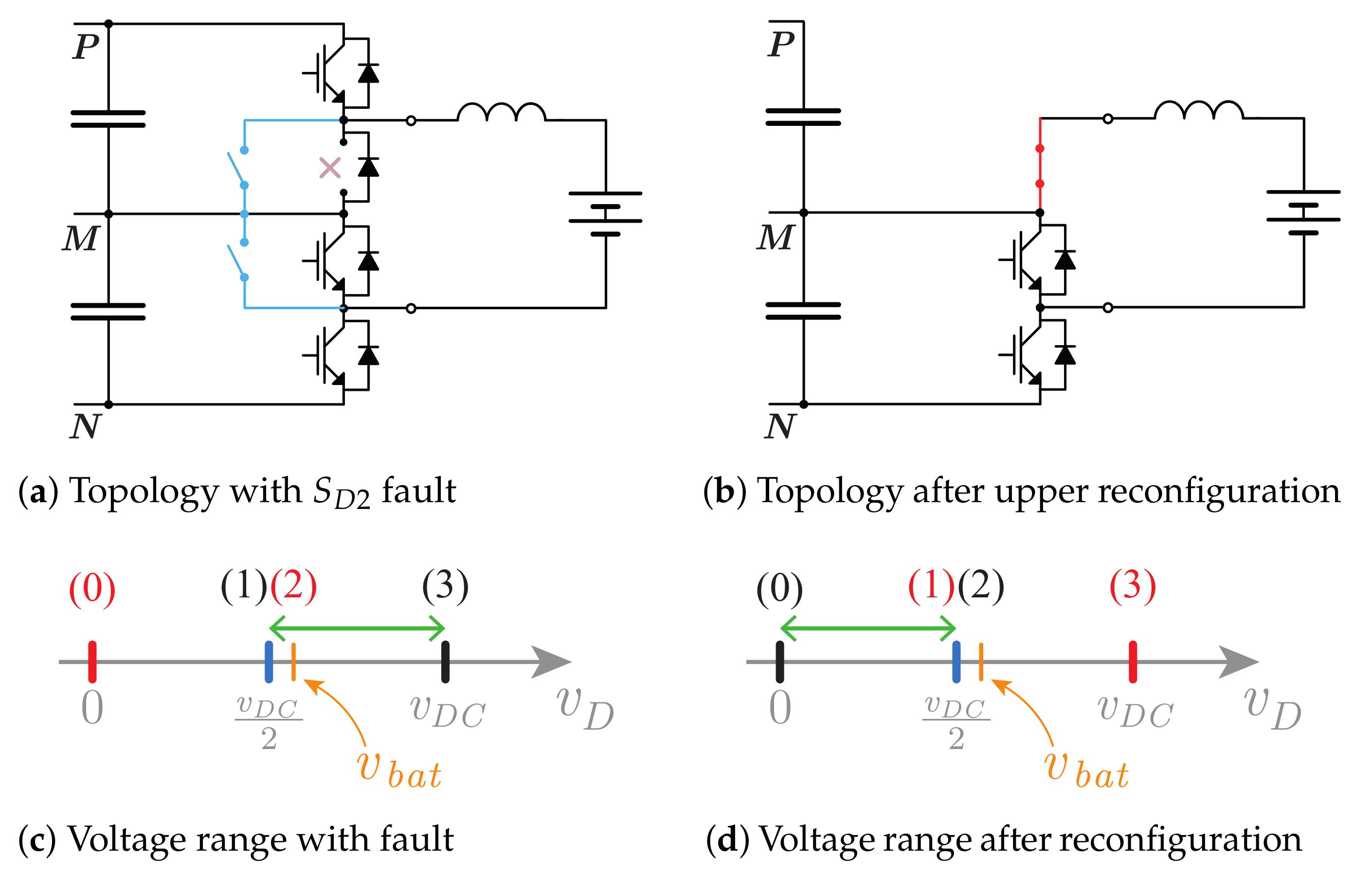
The proposed fault-tolerant UPS does not use redundant components and requires only minimal hardware expansion. Only 8 additional bidirectional switches are needed for fault tolerance (shown in red in
Figure 1). These can be relays, triacs or contactors, for example. This presents a relatively a low cost and complexity increase when compared to the standard (non-fault-tolerant) system.
The three converters in the UPS system are controlled using a Cooperative and Dynamically Weighted Finite-Control-Set Model Predictive Control technique, proposed in [
74]. This technique provides excellent dynamic response and steady-state performance, as well as improved converter cooperation. The use of a Model Predictive Control technique is highly advantageous for fault-tolerant purposes, since it allows the inclusion of advanced restrictions on the control-set, allowing the proposed technique to effectively limit/restrict the use of switching states affected by the existing fault in specific conditions. Since the used control technique is not the main focus of this work, it will not be discussed in detail in this paper (for more details, interested readers may refer to [
74]). Instead, only the specific changes made to the controller in the scope of the fault-tolerant operation will be described.
Even though the detection and identification of faults is critical for the correct activation of fault-tolerant measures, they can be studied separately from the fault tolerance approach. Hence, this paper will focus uniquely on the fault-tolerant techniques used to correct faults on the UPS power converters and not on the techniques used to detect and identify those faults. For the experimental implementation of this work, a fault diagnosis technique based on those proposed in [
89,
90] is used to trigger the proposed fault-tolerant measures.
5. Experimental Results
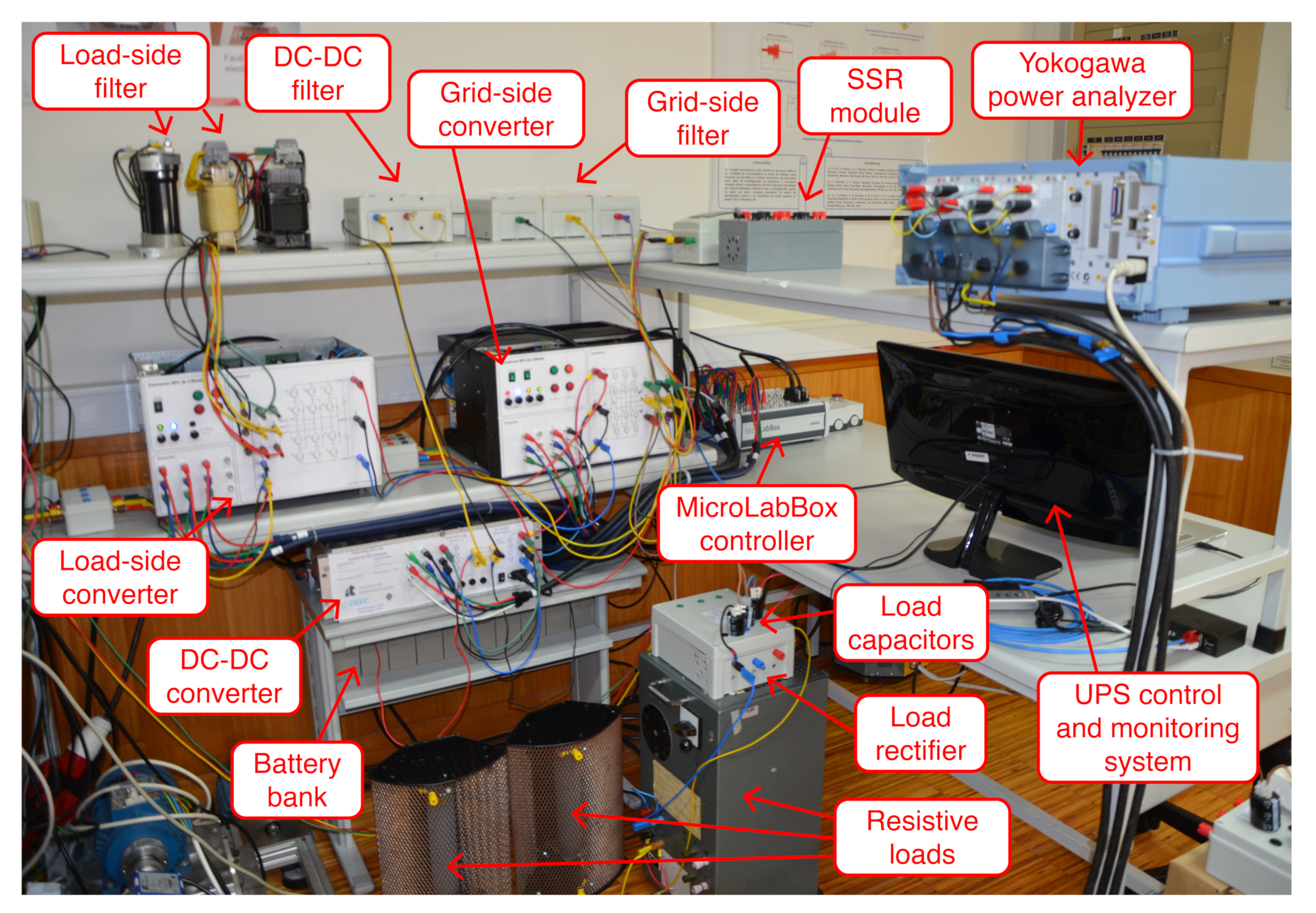
Experimental results are now presented, demonstrating the advantages of the proposed fault-tolerant technique. The prototype developed to test the proposed fault-tolerant UPS system is shown in
Figure 11.
All relevant circuit and controller parameters are shown in
Table 4.
For prototype safety, the grid voltage is adjusted to (rms) with an autotransformer and the DC bus reference in the absence of faults is set to . The UPS supplies a non-linear load, composed of a 3-phase resistive load ( resistors connected in ) connected in parallel with a 3-phase diode rectifier feeding a load. All controllers, fault diagnosis and fault-tolerant techniques are implemented in Matlab/Simulink and executed in real-time in a dSpace MicroLabBox platform, with a sampling time of . A Yokogawa WT3000 power analyzer is used to monitor system performance. Custom-made Mosfet-based SSRs are used to perform the hardware reconfigurations.
5.1. Normal UPS Operation
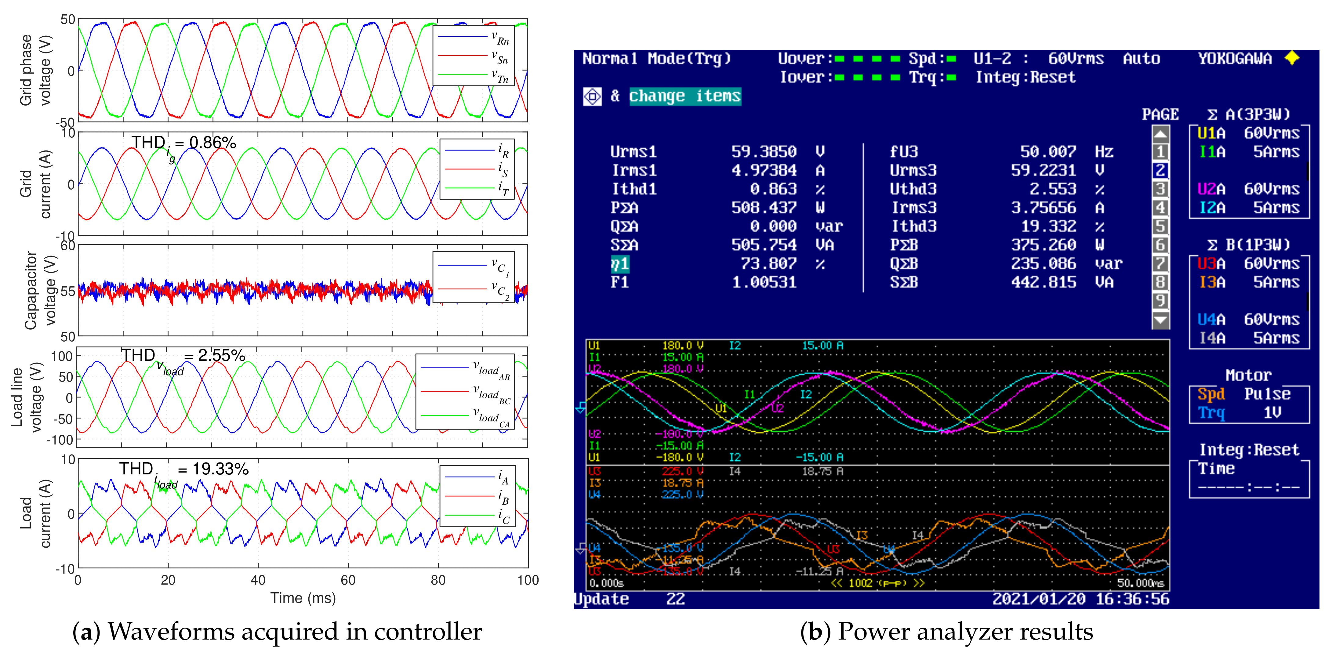
The steady-state performance of the proposed UPS is shown in
Figure 12. As seen in this figure, the load draws a highly distorted current from the UPS (
), but the UPS ensures low load voltage distortion (
), well within the acceptable range. The load draws a approximately
and
. The UPS draws approximately sinusoidal currents from the grid (
) with unity power factor. In these conditions, the CSG and LSC display an average switching frequency of approximately
and
, respectively. Given the low voltage and low power conditions used for prototype safety, the UPS displays an overall efficiency of approximately
in this test.
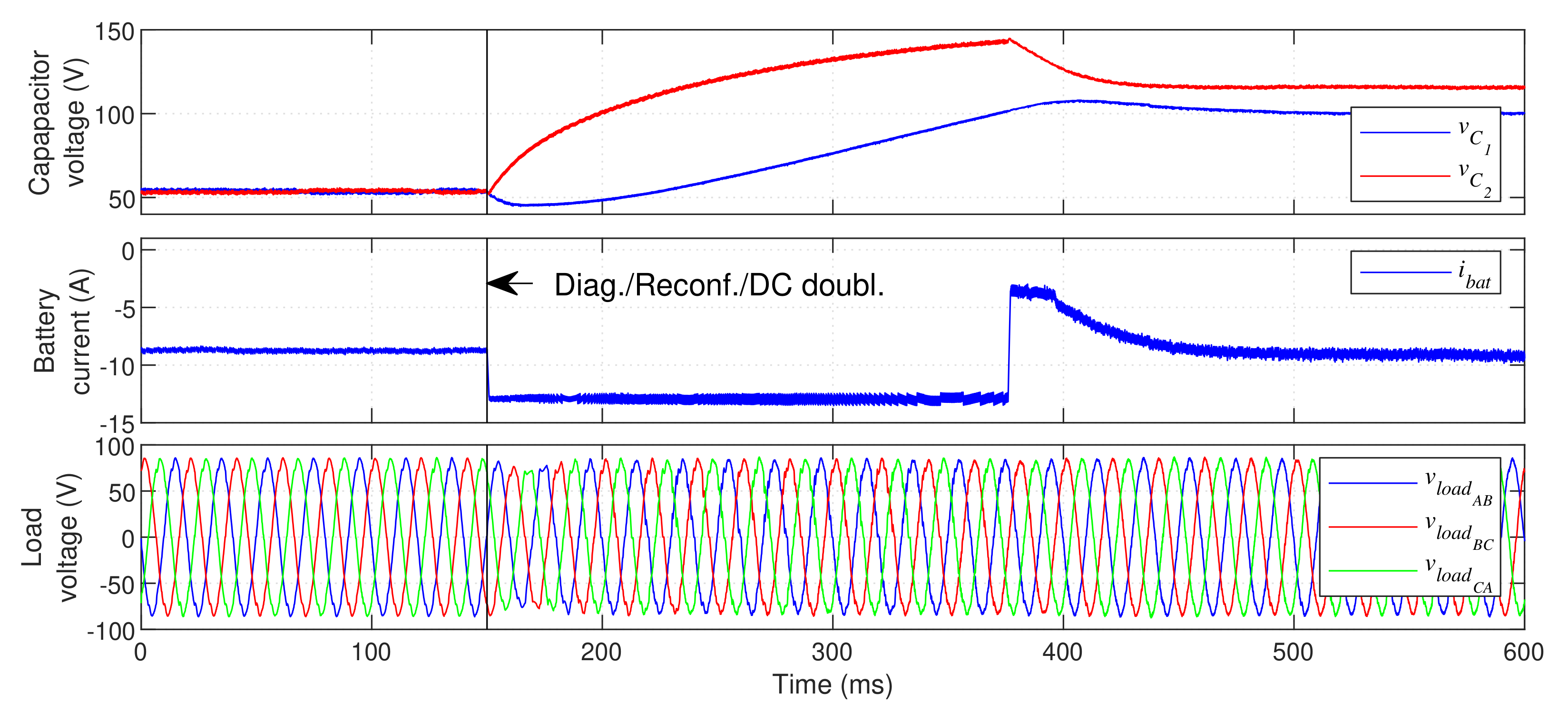
5.2. Grid-Side Converter Faults
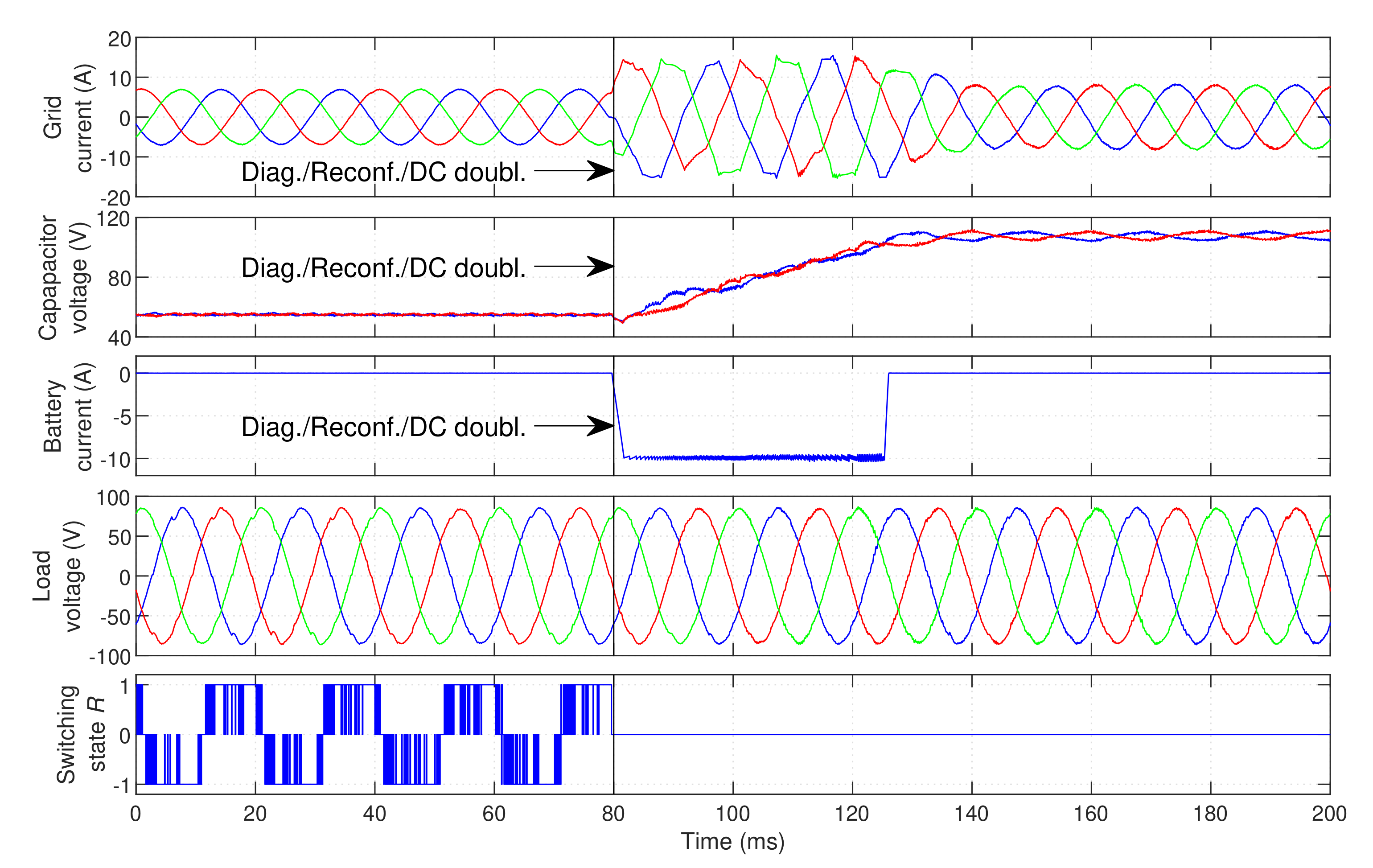
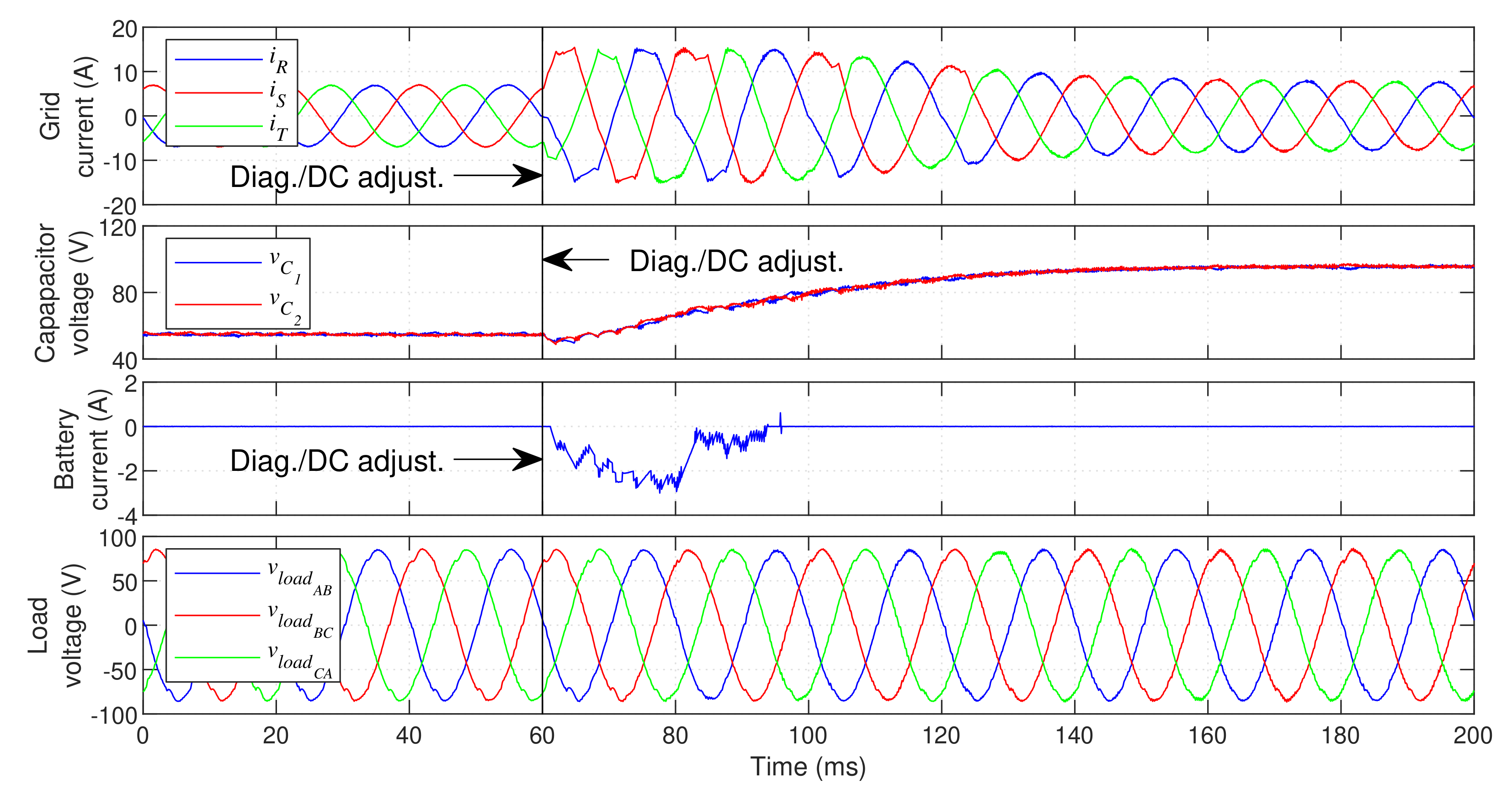
Figure 13 displays the fault-tolerant response of the UPS when a fault occurs in inner IGBT
.
An OC fault is created in IGBT
at
and is quickly identified. After the diagnosis, the reconfiguration is immediately performed and the DC bus voltage reference is doubled to
. As seen in
Figure 13, the switching state 0 is permanently selected in phase
R after the reconfiguration. As soon as the fault is detected, the GSC and DCC immediate increase their current references to the maximum defined value (
in the GSC and
in the DCC). This ensures that they supply the maximum possible power to the DC bus, in order to quickly charge it. After approximately
both capacitors surpass 90% of the target voltage (
per capacitor), returning the current references to their regular calculated value. This results in a very fast transition to post-fault operation. The load voltage is not affected by the fault or DC bus charging, continuously ensuring a high-quality voltage waveform at the critical load.
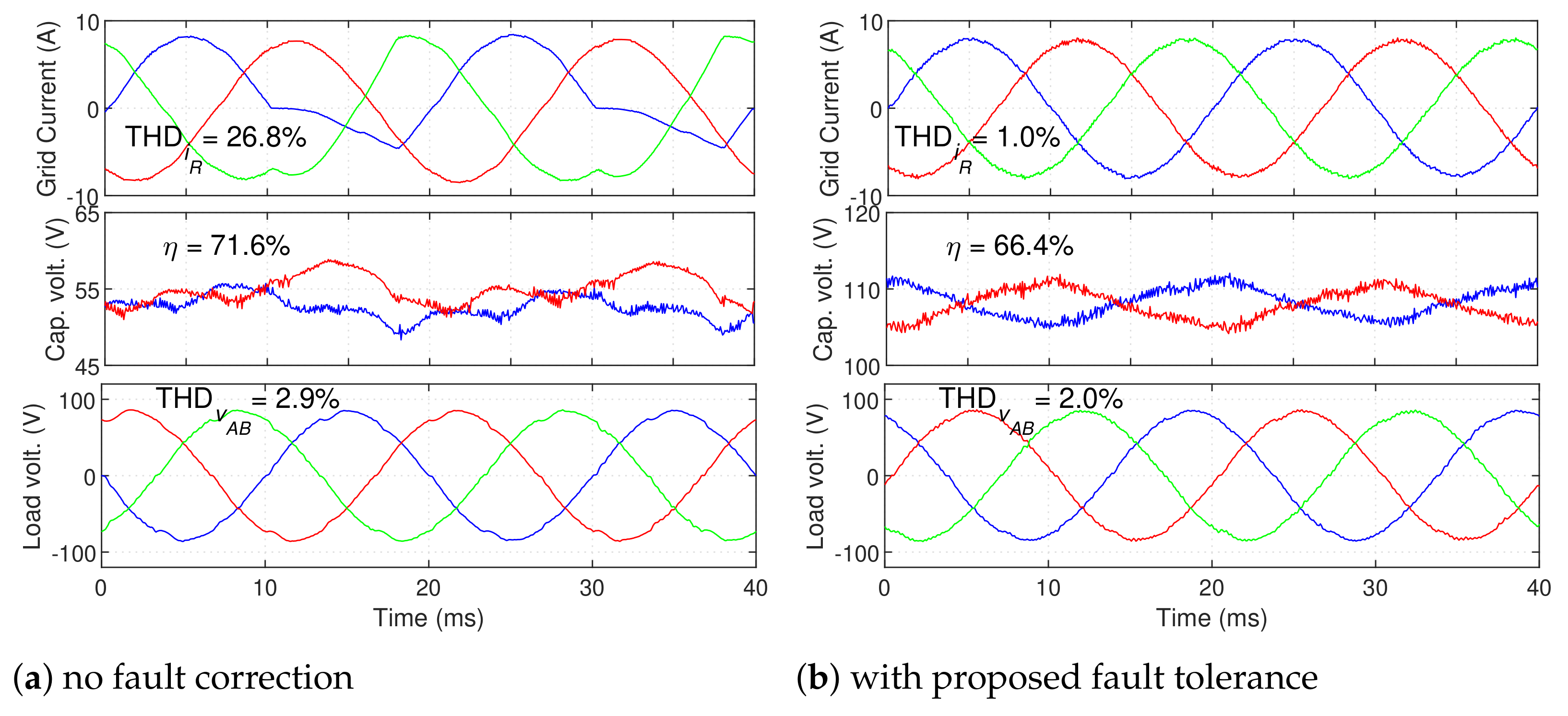
Figure 14 demonstrates the UPS operation in the presence of an
fault (with no correction) and the steady-state post-fault operation with the proposed technique. It is clear that an uncorrected fault severely degrades the grid current waveform, resulting in a very high THD.
On the other hand, with the proposed fault-tolerant solution the UPS presents approximately the same grid current distortion as in normal operation (). The THD of the load voltage waveform actually decreases in post-fault operation. Even tough this reduction seems contradictory, it can be easily explained. After the DC voltage is doubled, the LSC mostly uses the inner voltage vectors. However, since this converter is healthy, the outer voltage vectors are still available (with double the amplitude). These larger vectors provide faster compensation of the current spikes generated by the non-linear load, reducing the small “dips” caused by these spikes on the load voltage waveform and therefore reducing the overall THD. Thus, the harmonic content found on the UPS does not increase in post-fault operation. Even though phase R no longer presents switching (since it is permanently connected to the DC bus midpoint), phases S and T display a higher switching frequency than in normal operation (≈3.6 kHz). More importantly, the higher voltage and lack of medium voltage vectors (now located at the outside of the initial modulation area) lead to a significantly higher switching frequency on the LSC (close to compared to in normal operation). Consequently, the higher voltage applied to each semiconductor and higher switching frequency lead to increased converter losses. This is clear in the overall UPS efficiency, which drops from an initial 73.8% to approximately 66.4%.
This demonstrates that an efficiency reduction is expected in post-fault conditions. However, it must be noted that the amplitude of this reduction is not representative of the one expected in an industrial system. Since very low power is drawn from the UPS in this test, even a small increase in losses produces a significant efficiency reduction. In high-power operation, the efficiency should be reduced, but not in such a considerable way. Even with this efficiency reduction, fault tolerance is highly advantageous, since it allows the system to remain in operation until the fault is repaired.
It is also clear from
Figure 13 that the capacitor balance is reduced after the fault, resulting in higher capacitor voltage oscillation than in normal operation. Despite the efficiency reduction, the UPS successfully maintains operation in the same conditions after the fault, without compromising the operation of the critical load.
The fault correction procedure in case of an outer IGBT fault (in
) is shown in
Figure 15. The fault is detected at
and the converter immediately triggers the DC voltage adjustment. As seen in the figure, the grid currents are distorted while the DC bus increases, but resume sinusoidal waveform once the DC bus approaches its target voltage. In this case, the DC bus voltage is not doubled, but increased only to the voltage value calculated using (
4).
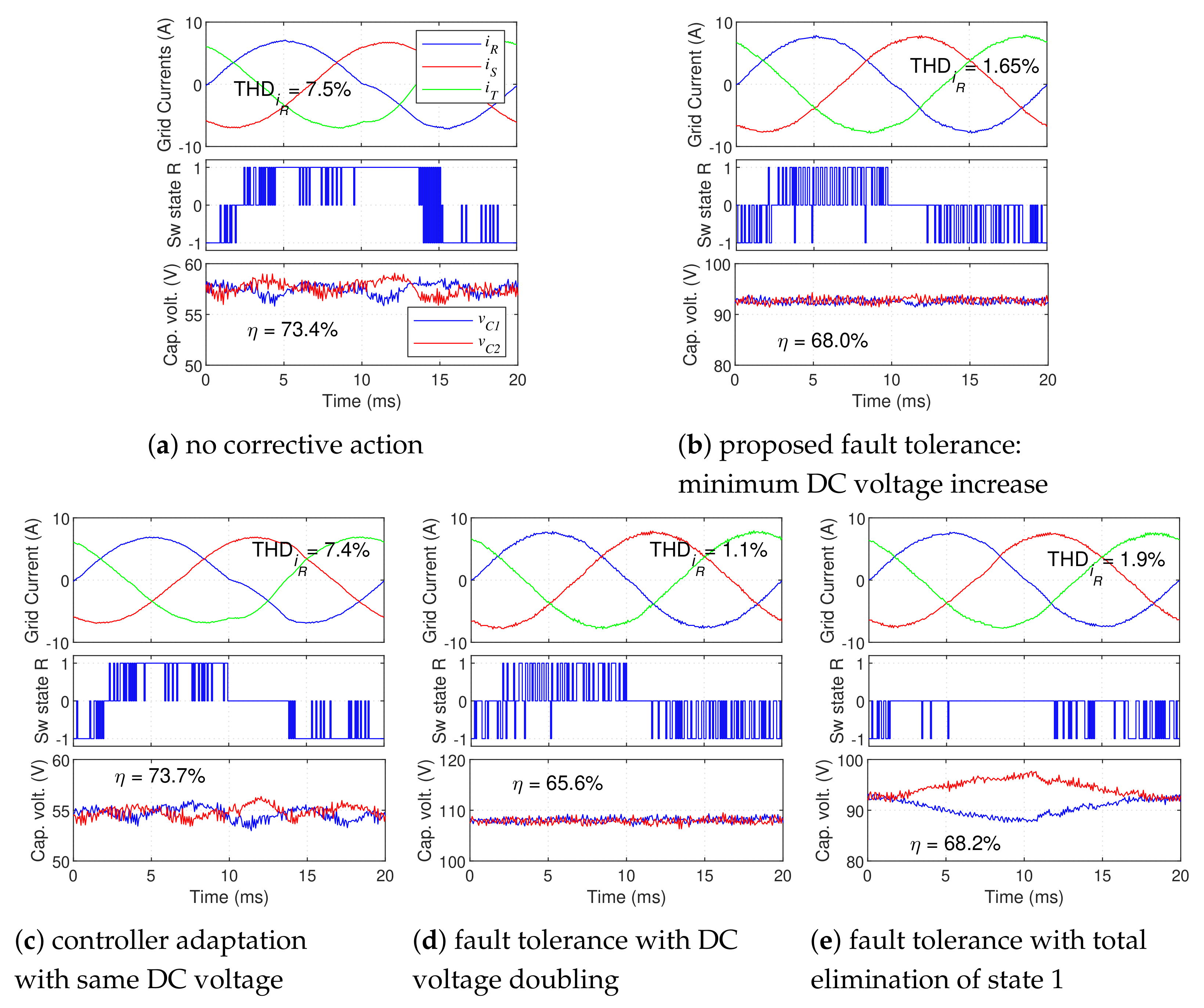
The advantages of the proposed technique in steady-state are shown in
Figure 16.
From
Figure 16a it is clear that this fault only affects the converter for a short portion of the period, during the transition to negative current (as seen in
Figure 5). Nonetheless, it causes significant grid current distortion, which needs to be corrected. As shown in
Figure 16b, the proposed technique reduces the current THD to approximately
. Several design choices made in the fault-tolerant technique can be better understood by studying
Figure 16c–e.
Figure 16c clearly demonstrates that without adjusting the DC bus voltage, an acceptable correction may not be possible (depending on the operating conditions). Comparing
Figure 16b,d, one can conclude that a higher THD reduction would be possible by doubling the DC bus voltage, instead of performing a minimal DC bus voltage increase. However, a higher DC bus voltage also leads to higher switching losses in both the GSC and LSC—with full DC bus voltage doubling, the average GSC/LSC switching frequency is
/
vs.
/
in the minimal voltage increase case—consequently causing lower UPS efficiency (65.6% vs. 68%). This is why a minimal voltage increment is advantageous.
It is important to note that the minimal voltage increase in this case was quite significant (from
to approximately
—roughly a 68% increase). This is mainly due to the very low grid voltage used in the tests (for prototype safety). If higher voltage is used, a significantly lower voltage increase would be seen (proportionally). For example, with a grid voltage of
,
DC bus and the converter drawing
from the grid, Equation (
4) would result in a minimum DC voltage of approximately
—a 19.5% increase. Thus, in industrial applications this approach will carry even higher advantage than demonstrated by these results.
Finally,
Figure 16e demonstrates the UPS performance obtained with a complete elimination of the affected switching state (1) from phase
R. This approach reduces the control versatility more than the proposed solution, since the state cannot be used in the conditions in which it is not affected by the fault. Even though this does not compromise the modulation area, it reduces the DC bus balancing capabilities of the converter, which leads to higher DC bus unbalance (clearly seen in the figure), as well as a higher grid current THD. This clearly demonstrates the advantages of using the proposed selective switching state exclusion technique.
Figure 17 displays the case of a fault in clamp diode
of the GSC. As shown in
Figure 17, the proposed technique is able to correct the clamp diode fault merely through software adaptations.
If no corrective action is taken, the current in the faulty phase
R is slightly distorted, as seen in
Figure 17a. More importantly, the unexpected voltage output of the affected switching state leads to erroneous DC bus power calculation, which raises the DC bus voltage level (from
to about
). By avoiding the affected control state, this problem is entirely avoided and the grid current THD remains similar to pre-fault conditions. As before, the proposed selective state exclusion promotes better DC bus voltage balance than a full state exclusion. In this fault case, the DC bus voltage remains the same and the switching frequency is not significantly altered, resulting in approximately the same efficiency as in normal operation.
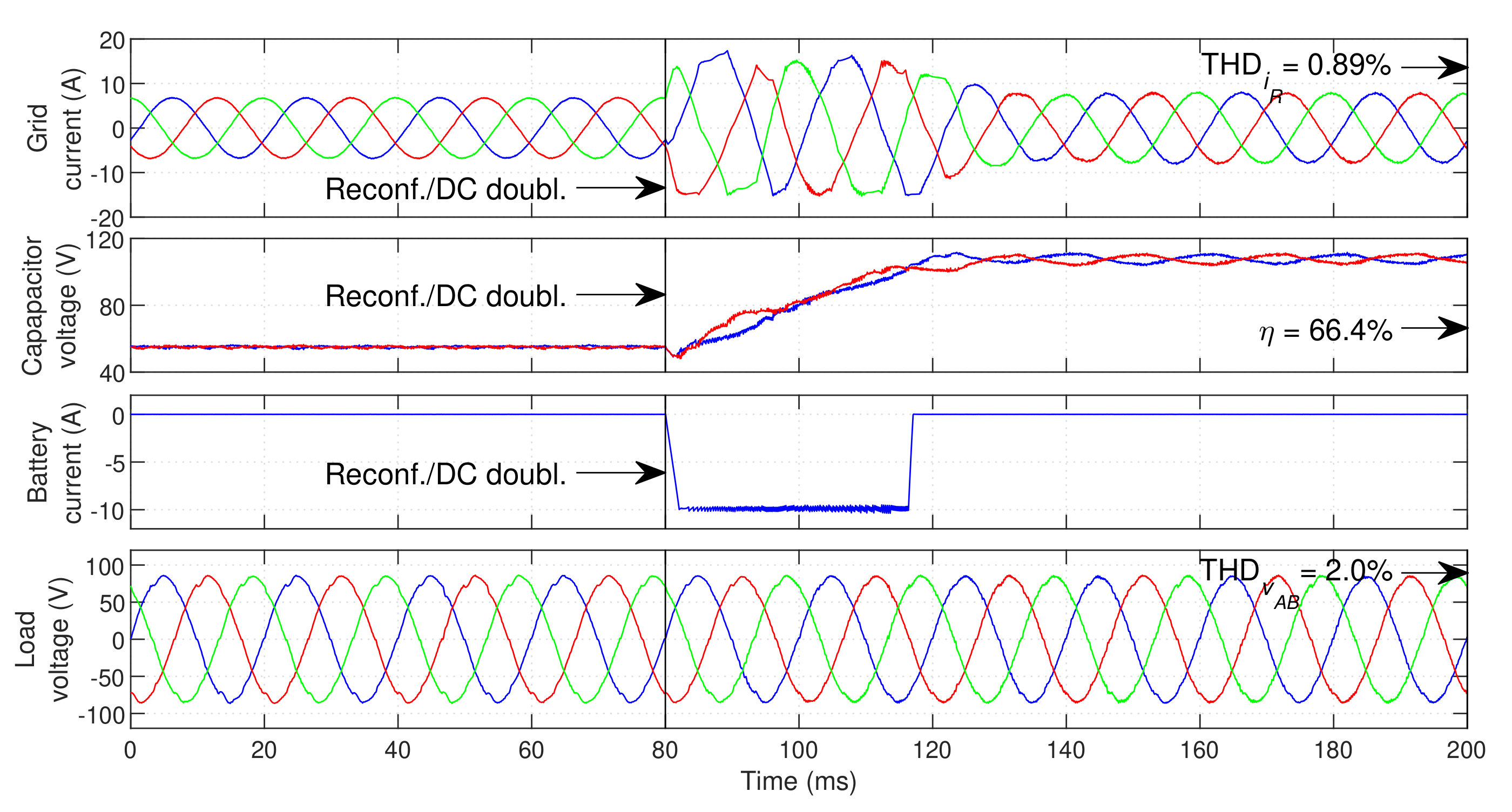
Since anti-parallel diode faults could be potentially destructive for the developed prototype, due to the high voltage spikes caused by the sudden phase current elimination, this type of fault was not tested experimentally. Instead, the fault-tolerant procedure was triggered without an actual fault, merely to demonstrate the transient and post-fault performance with this type of fault. This is illustrated in
Figure 18.
As in previous cases, the DC bus voltage reference is immediately doubled and the controller selectively avoids the switching states that use the faulty diode (thus avoiding causing additional voltage spikes). During the DC bus voltage doubling the grid currents are considerably distorted, but resume operation with low distortion as soon as the target DC voltage is reached ( in steady-state). The load voltage THD is reduced, as previously explained. As before, a UPS efficiency reduction is observed in fault-tolerant operation.
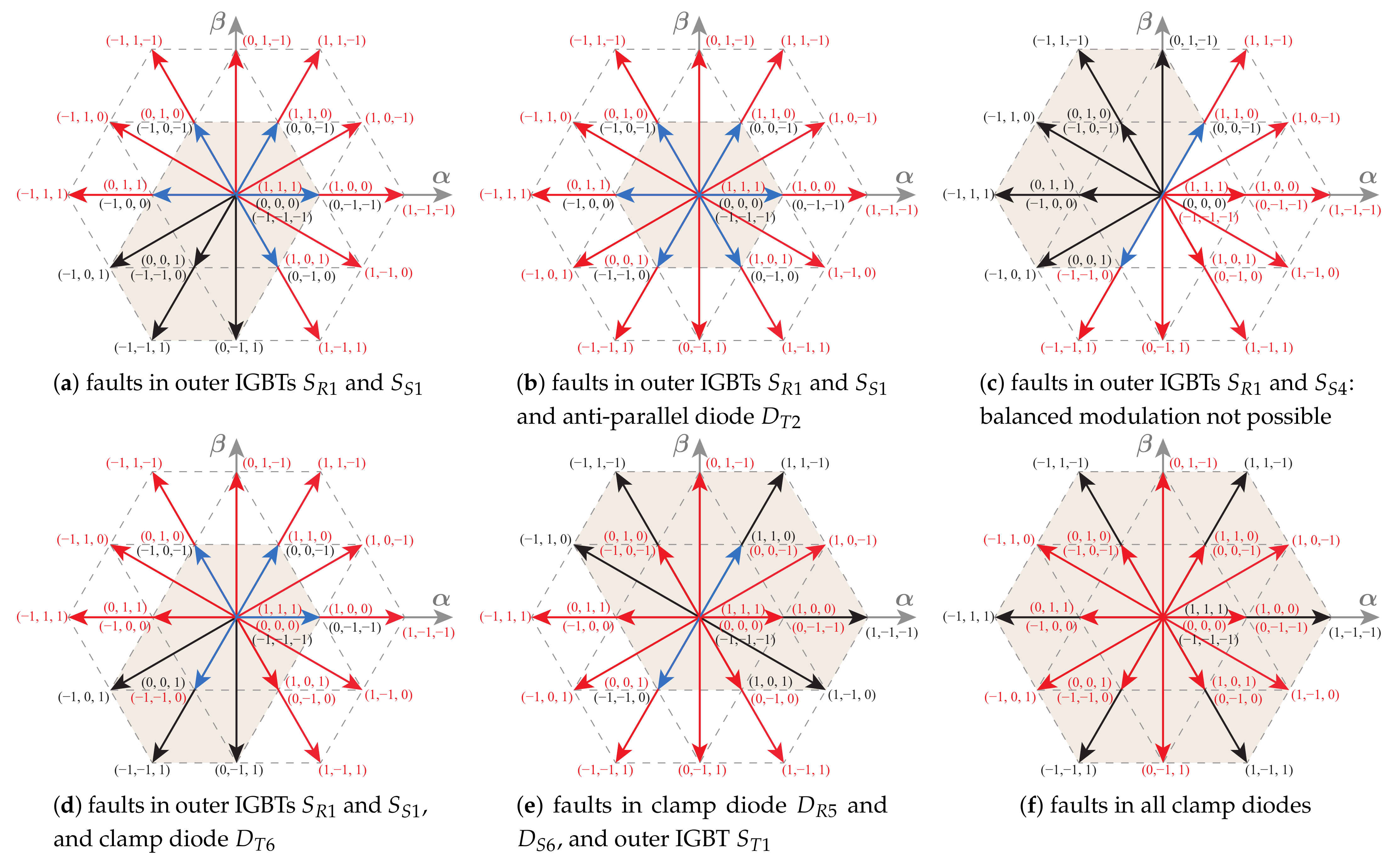
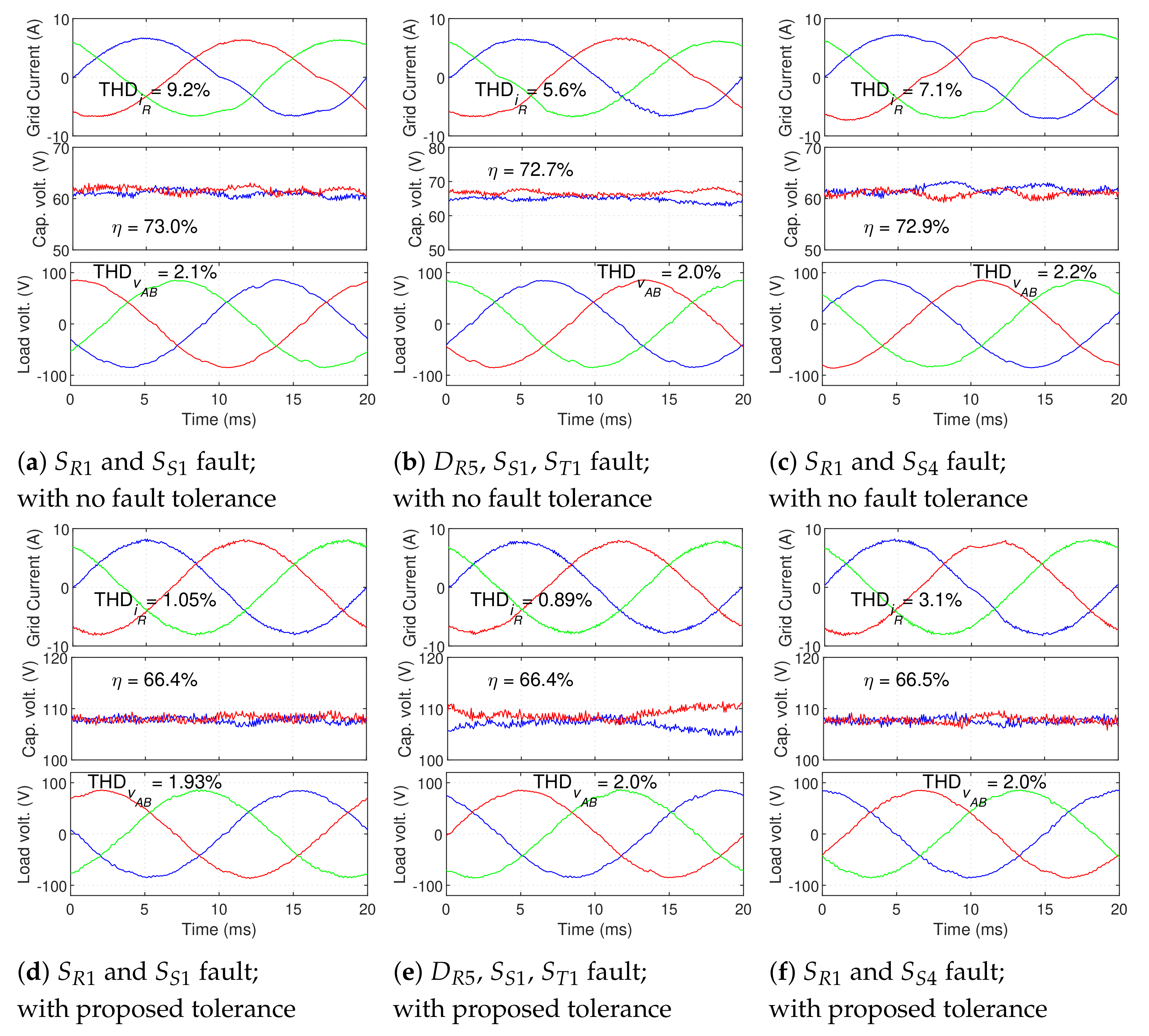
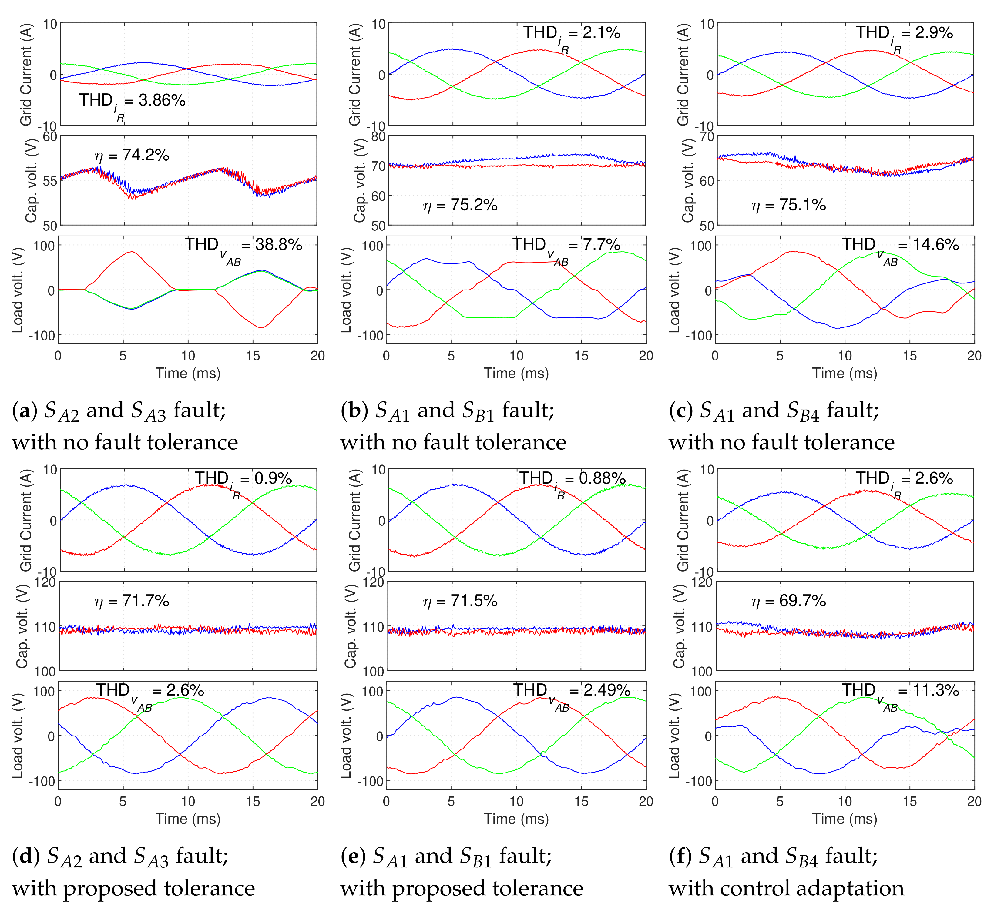
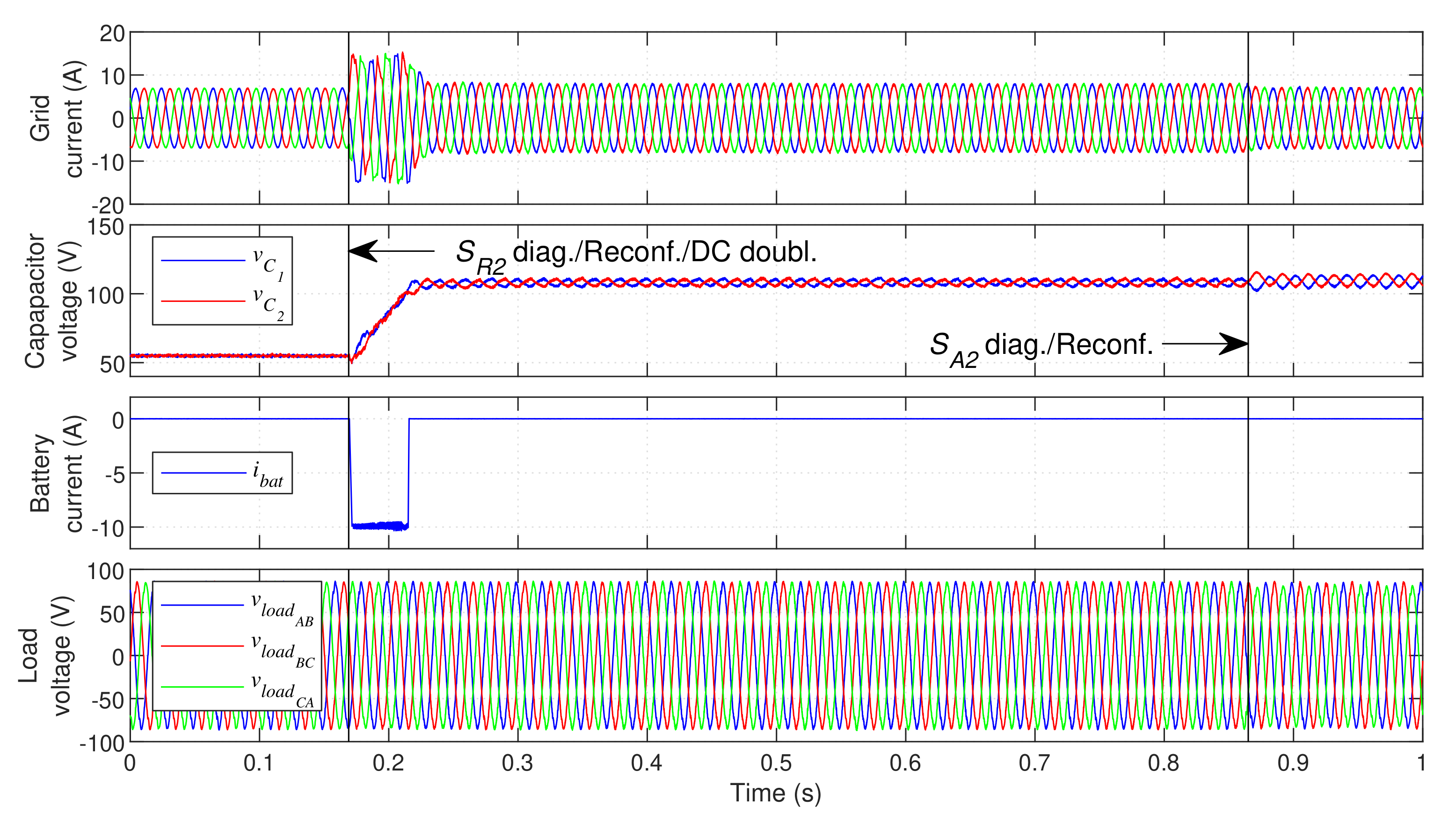
Figure 19 demonstrates the corrective potential of the proposed technique in cases where multiple simultaneous faults exist in the GSC.
The UPS post-fault performance in each presented case is demonstrated with no corrective action (on top) and with the proposed fault-tolerant mechanism (on the bottom). In all cases, it is clear that the proposed technique significantly reduces the impact of the faults on the grid current waveform and on the DC bus voltage level (which tends to deviate from the intended reference when in the presence of faults). The load voltage waveform also tends to slightly improve. In the first and second cases, the post-correction THD values are similar to those found in normal operation (lower in the case of voltage THD, as previously explained)—seen in
Figure 19d,e. The third case, shown in
Figure 19c,f, represents the case of two faults in outer IGBTs, located both in an upper a lower half-leg (
and
). From
Table 1, this type of fault cannot be completely corrected, since it is impossible to recover a full modulation area. Nonetheless, the proposed technique is able to significantly reduce the effect of the fault, leaving the resulting grid current THD with an acceptable value (
). This demonstrates that even in cases in which a full modulation area cannot be obtained, the doubling of the DC bus and the proposed selective state exclusion can provide acceptable post-fault performance. In all cases, GSC/LSC switching frequency significantly increases after the DC voltage doubling (to slightly over
/
), once again leading to an efficiency reduction.
5.3. Load-Side Converter Faults
Experimental results are now presented for the case of faults in the LSC.
Figure 20 demonstrates the steady-state UPS operation after a fault in IGBTs
and
, when no corrective actions are applied. As visible, these faults have a very high impact on the load voltage waveform, especially in the inner IGBT case. These faults severely distort the load voltage waveforms and alter their RMS value, which can compromise the operation of the protected critical load.
Figure 21 displays the response of the proposed fault-tolerant UPS when a fault occurs in inner IGBT
of the LSC.
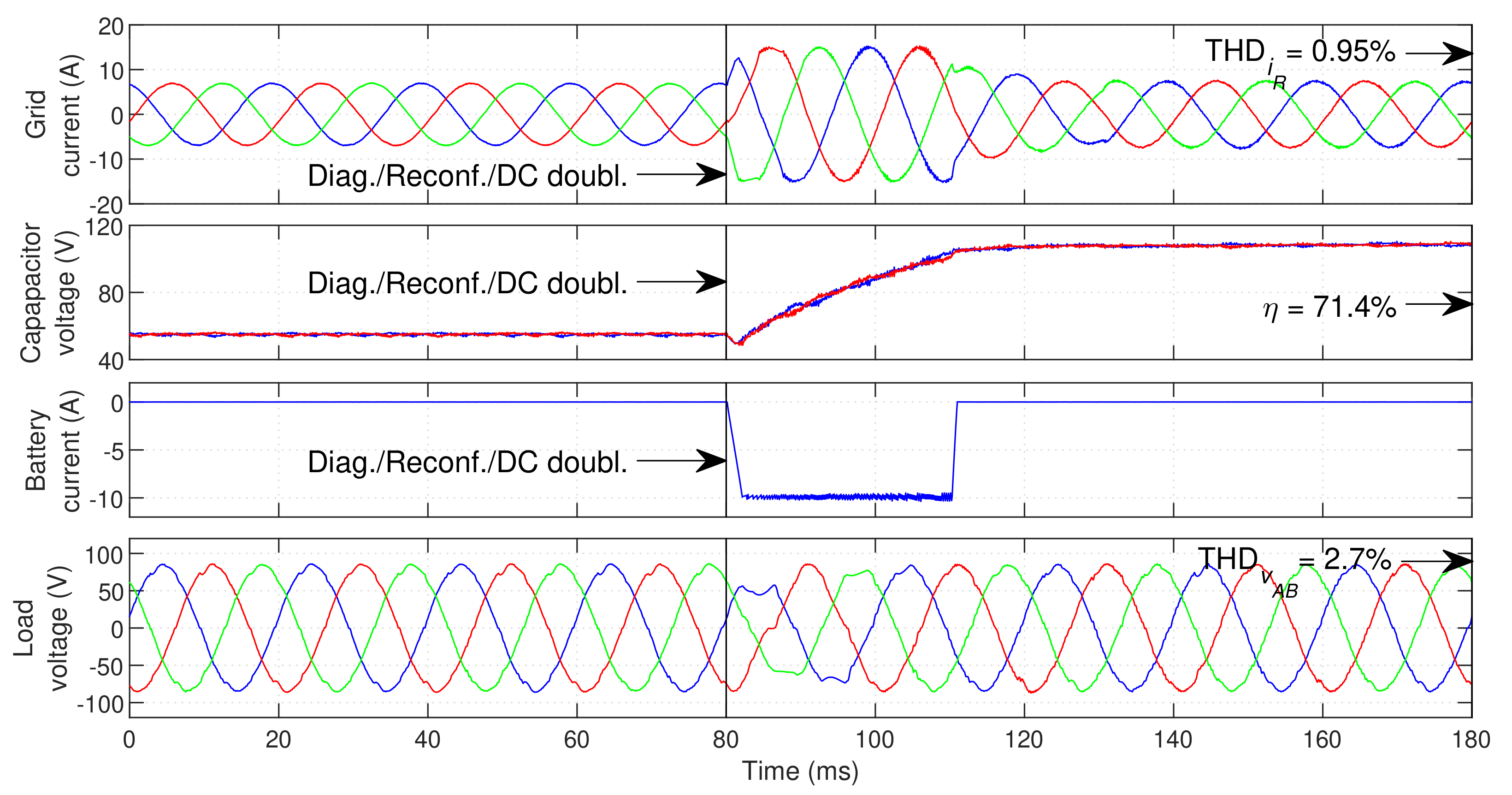
The fault occurs at and is quickly identified. The DC bus voltage reference is immediately doubled and the controller avoids the affected switching states. The GSC and DCC immediately begin to inject as much power as possible into the DC bus, raising its voltage to the new reference value () in little over . The grid-current distortion remains close to the pre-fault values. The load voltage distortion after the reconfiguration is not significantly increased (raises from 2.55% to 2.7%). During the transient, the load voltage is distorted (mainly in phase A). However, this distortion is relatively mild and lasts only for about one fundamental period, which should not compromise the critical load operation. The DC bus capacitors balance is not significantly affected by LSC faults, since the GSC is the main responsible for maintaining the DC bus capacitors balanced. In post-fault operation, the GSC switching frequency increases to approximately . The switching frequency in phases B and C of the LSC increases to approximately . Thus, the system displays switching frequencies significantly lower than in the case of GSC faults. In addition, phase A no longer has switching losses, since a hardware reconfiguration is performed. This results in an overall efficiency considerably higher than in the case of GSC faults—system efficiency is reduced from 73.8% to 71.4%.
The response of the proposed fault-tolerant system when a fault occurs in outer IGBT
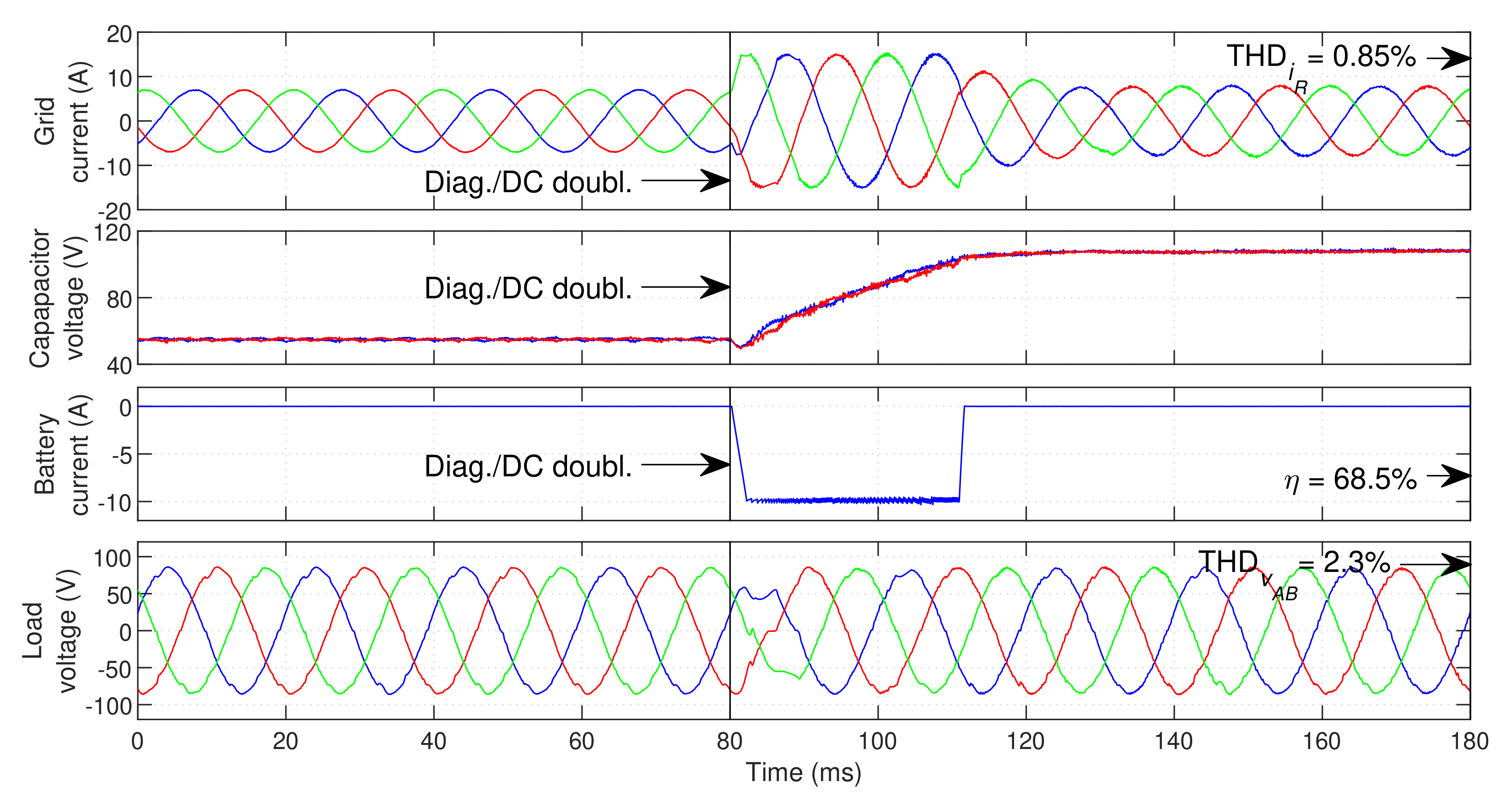
is displayed in
Figure 22.
In this case, as seen in the decision process in
Figure 6, no hardware reconfiguration is performed. The DC bus voltage doubling is similar to the previous case. Since a reconfiguration is not performed, the LSC retains higher control versatility, which is why it can achieve lower load voltage distortion than in the previous case (
). In this case, the load voltage distortion during the transient is corrected even faster than in the previous case. Hence, the critical load operation is not affected by the fault. With this type of fault, the average switching frequency in post-fault operation is higher than in the previous case (
in the GSC and ≈
in the LSC, with all phases in operation). For this reason, a lower efficiency is obtained.
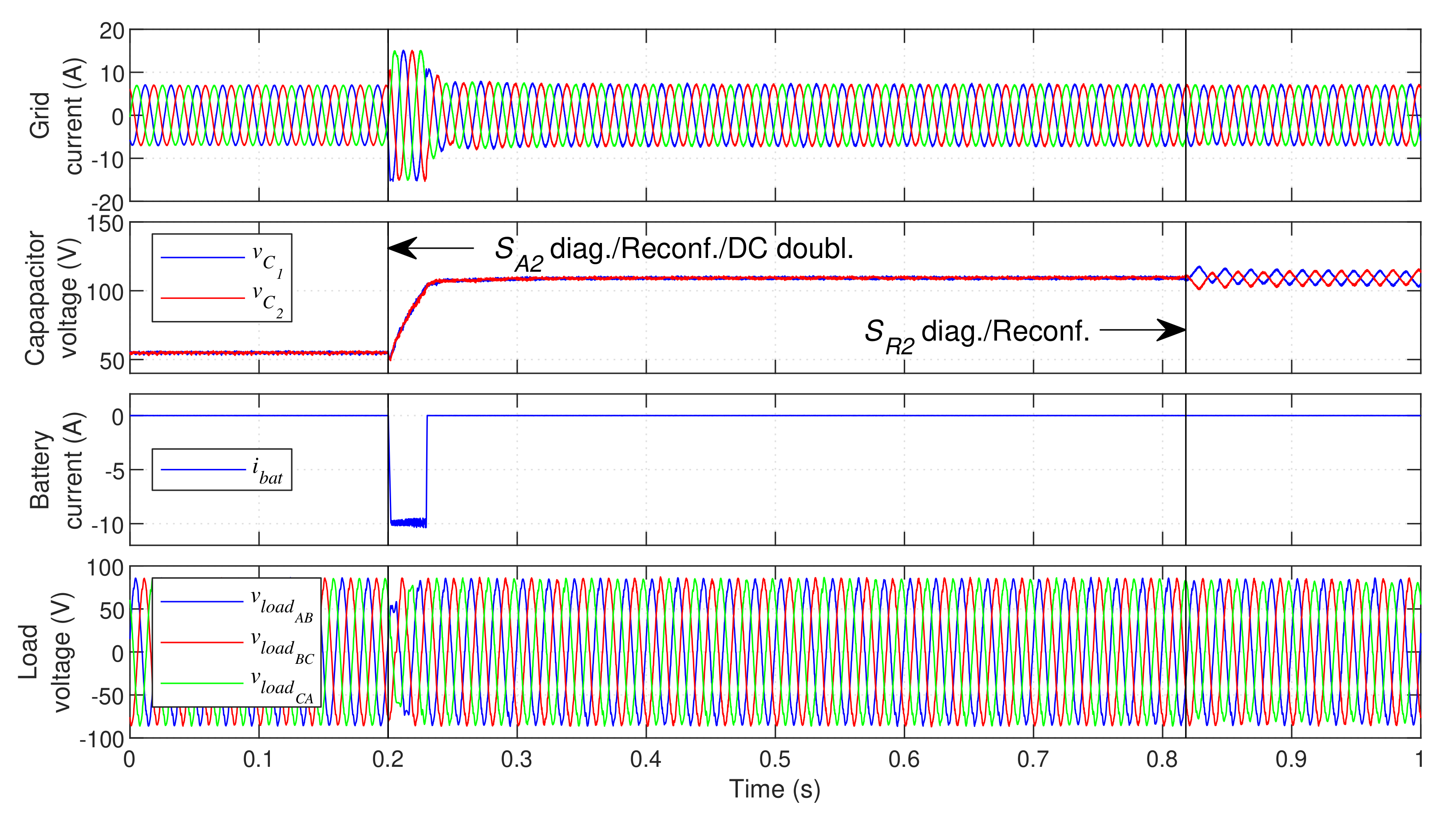
The clamp diode and anti-parallel cases are similar to those presented for the GSC (and are therefore omitted). Some cases of multiple simultaneous faults in the LSC are shown in
Figure 23, without any fault correction (on top) and with the proposed fault-tolerant scheme (on the bottom).
The first case, shown in
Figure 23a,d represents the case of 2 faults in the same phase (IGBTs
and
). As seen in
Figure 23a, these faults critically compromise the load voltage waveform when uncorrected. On the other hand, when the proposed fault tolerance is used, these 2 faults can be corrected through the reconfiguration of phase
A and the doubling of the DC bus voltage. As seen in
Figure 23d, the UPS keeps similar grid current and load voltage distortion after the fault. As in the previous cases, the overall UPS efficiency is reduced, but is considerably higher than in the case of GSC faults.
The second case, displayed in
Figure 23b,e, represents the case of 2 faults in outer IGBTs in different phases, both in the upper half-leg. In this case, the fault can be completely corrected, resulting in performance similar to the pre-fault operation (with a lower efficiency).
The case in
Figure 23c,f represents one of the cases in which a complete modulation area cannot be achieved—two outer IGBTs in different half-legs (
and
, in this case)—refer to
Table 1. As predicted, these two faults cannot be completely compensated by the proposed technique. Unlike the analogous case of GSC faults (in
Figure 19f), sufficient fault mitigation cannot be achieved and significant voltage distortion is seen on the load voltage waveform (
), which will most likely compromise the operation of the critical load.
Nonetheless, several cases of simultaneous multiple faults can be effectively corrected in the LSC.
5.4. DC-DC Converter Faults
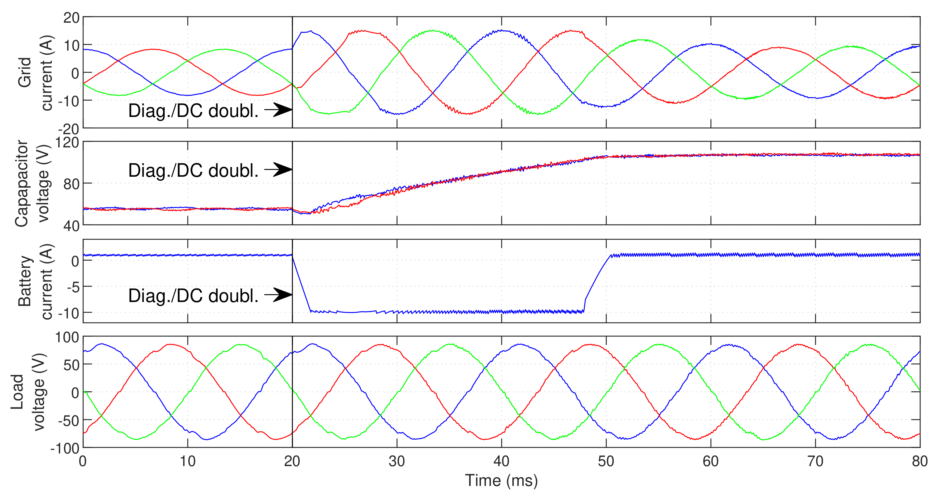
Results are now presented demonstrating the performance of the system when an OC fault occurs in the DC-DC converter.
Figure 24 demonstrates the UPS operation when a fault occurs in outer IGBT
of the 3LDC converter, while the batteries are being charged.
As visible in
Figure 24, the batteries are initially being charged with a
current. Then, at
, an OC fault is created in IGBT
. The DC bus voltage reference is immediately doubled. Both the GSC and the DCC immediately begin charging the DC bus. The fault in
does not affect the discharging of the batteries, so the DCC can contribute to raise the DC bus voltage without restrictions. As the DC bus is charged, the DCC resumes battery charging. At this point, correct operation with positive current is already possible and a normal operation is resumed.
Figure 25 displays the case of a fault in inner IGBT
. The UPS operates in stored energy mode when the fault occurs, with the DCC supplying all energy to the load.
When the fault is identified, at , the reconfiguration is immediately performed, which restores the ability of the converter to generate negative current. Simultaneously, the DC bus voltage reference is doubled. This makes the DCC draw as much power as possible from the batteries, in order to raise the DC bus voltage. In this particular case, since the UPS operates in stored energy mode, the GSC cannot contribute to raise the DC bus voltage, making DC bus charging slower. To minimize this problem, the DCC can draw higher current from the batteries to speed up this process (effectively operating in overload for the duration of the process). This is possible because batteries typically support higher discharge currents for short periods (higher than the rated continuous discharge current). Since the DC charging process is usually fast (the DCC operates in overload only for approximately in this test), this does not pose a risk for the batteries. In the experimental tests, the battery overcurrent limit established for this period is . Depending on the used battery type and characteristics, this overcurrent limit can be significantly higher (for example, with lithium batteries)—the higher the current drawn from the batteries, the faster the transition to post-fault operation.
After the reconfiguration, the DCC looses its ability to balance the DC bus capacitors, and is only able to charge capacitor
. Thus, as the converter tries to raise the DC bus voltage, it also significantly increases the unbalance between the two capacitors (reaching values as high as
—visible in
Figure 25). This case is particularly affected by this limitation because the GSC is not available in stored-energy mode and cannot contribute to the DC bus balance. The LSC contributes to correct this unbalance, but due to the higher priority given by this converter to the output voltage waveform the capacitor balancing is relatively slow. Due to an initial drop in
voltage, the load voltage waveform is slightly affected for approximately 2 fundamental periods (with a small reduction of peak value).
Approximately after the fault, at , steady-state is reached. Since the DCC can only charge capacitor , the LSC is the only converter responsible for maintaining capacitor balance. Thus, an unbalance of approximately is maintained in steady-state. The overall post-fault unbalance could be lowered by raising the relative weight of the DC bus balancing objective in the LSC global FCS-MPC cost function, but this would lead to a degradation of the load voltage waveform. This unbalance (approximately 7% of the total DC bus voltage) is not ideal, but does not compromise the continuous operation of the UPS in fault-tolerant mode, especially since the UPS can only remain in stored energy mode for a relatively short period of time (until the batteries are depleted). It is also important to note that this case is relatively unlikely, since a UPS rarely operates in stored energy mode (only when the grid fails) and only for short periods of time. Despite this, the proposed fault-tolerant solution ensures a continuous and uninterrupted load supply in any fault case.
5.5. Multiple Converter Faults
The ability of the proposed non-redundant fault-tolerant scheme to correct faults in multiple converters simultaneously is demonstrated in
Figure 26 and
Figure 27.
In
Figure 26 a fault in inner IGBT
of the GSC is created first. The fault is quickly identified, and the hardware reconfiguration is performed in phase
R of the GSC. The DC bus voltage reference is immediately doubled. At
, a fault in inner IGBT
of the LSC is created. The reconfiguration is immediately performed in phase
A of the LSC and, since the DC bus voltage is already doubled, post-fault operation is immediately achieved (with a practically instantaneous transition). After the second fault occurs, a higher DC bus capacitor voltage oscillation can be observed. Nonetheless, this is not significant and does not affect the UPS operation.
In
Figure 27, the same two faults occur, but in reverse order. Thus, as the LSC fault happens first, the LSC needs to wait for the DC bus voltage doubling to achieve post-fault operation, leading to a short period of slight voltage waveform distortion, as seen in
Figure 21.
When the GSC fault occurs, its transition to post-fault operation is practically instantaneous, since it does not need to wait for the DC bus voltage doubling.
As this example demonstrates, the proposed non-redundant fault-tolerant strategy allows the correction of simultaneous faults in different converters, retaining full-rated capabilities. Faults can be corrected simultaneously in all converters of the UPS.
6. Discussion and Conclusions
As described in
Section 3 and
Section 4 and demonstrated by the experimental results in
Section 5, the proposed fault-tolerant technique has a very high fault correction potential, especially since this is a non-redundant system. In this section, the advantages, disadvantages and industrial applicability of the proposed technique are discussed in light of the presented results and the most important conclusions are presented.
Fault-tolerant solutions in the literature mostly focus on IGBT OC faults, with only a few solutions considering clamp diode faults. On the other hand, the proposed fault-tolerant technique can correct OC faults in all semiconductors of the UPS—IGBTs, their respective anti-parallel diodes, and the clamp diodes—resulting in a very comprehensive correction solution. Additionally, the proposed technique provides fault tolerance not only in the 3-level NPC converters, but also in the 3-level DC-DC converter—something not done before.
The proposed system requires a low amount of additional hardware, adding little complexity to the system topology—only three bidirectional switches are required for each 3-level NPC converter and only two switches for the 3-level DC-DC converter (a total of eight switches). On the other hand, since the fault-tolerant procedure requires (in some cases) a doubling of the DC bus voltage, the minimum voltage rating of the DC bus capacitors and all the IGBTs is doubled. A higher component voltage rating can significantly increase the system cost, especially in high-voltage systems. When the required IGBT voltage ratings are close to the limit of current technology, raising the voltage rating may exponentially increase system cost, rendering the solution unfeasible. For this reason, this solution is unlikely to be economically viable in medium to high-voltage applications.
Nonetheless, 3-level converters are also used industrially in low voltage systems (such as in high-power datacenter UPS systems), due to their higher power quality, lower losses and smaller filtering requirements. In this type of system, the required IGBT voltage in a 3-level converter is relatively low. Thus, even when the voltage requirements are doubled, the IGBTs still falls within a very commonly used voltage range, which means the price increase is not overwhelming. In these cases, even though the UPS cost increase is not negligible, it is acceptable given the increase in system resilience. Consider the example of a datacenter UPS: the UPS system typically feeds only low voltage loads and needs to be extremely reliable. If, for example, a DC bus voltage of 800V is used, each IGBT would need to be rated at in a regular system or in the proposed fault-tolerant solution. Nowadays, IGBTs up to are extremely common, which makes them relatively affordable. Hence, even though the required investment is not negligible, the significantly higher reliability of the proposed fault-tolerant system justifies it, especially in highly critical facilities, such as high-tier datacenters, in which resilience is the top priority.
The proposed technique allows all UPS converters to retain full modulation capacity after internal faults. This avoids derating the system and ensures that the critical load can continue to operate in the same conditions, regardless of the fault.
Previous work in the literature has used the hardware reconfiguration adopted for the 3-level NPC converters. However, the reconfiguration is typically performed whenever a fault is detected, regardless of its type. The proposed fault-tolerant solution performs this reconfiguration only when strictly necessary—in case of 3LNPC inner IGBT fault or multiple faults in the same phase, or in the case of 3LDC inner semiconductor fault (IGBT or diode). Thus, a reconfiguration is avoided in most cases. By avoiding an unnecessary reconfiguration, the faulty converter retains more usable switching states, ensuring higher control flexibility and minimizing the fault impact on the overall UPS performance.
The increasing of the DC bus voltage leads to increased losses in the converter, reducing its efficiency. However, this is not a critical problem, for two reasons: (1) the main objective of the UPS is protect the critical load, which is ensured by the proposed technique; (2) the UPS will only work in fault-tolerant conditions for a relatively short period, until the faults are repaired. Nonetheless, a minimal DC bus voltage increase technique is also proposed specifically for the case of outer IGBT faults in the GSC. This approach allows the correction of this type of fault with lower DC bus voltage increase, which leads to a lower UPS efficiency reduction in post-fault operation.
Unlike most solutions found in the literature, the proposed solution does not entirely prevent the converter from using the switching states affected by the fault. Instead, the adaptations made to the FCS-MPC controller ensure that the switching states affected by the fault are selectively avoided only in the conditions in which the faulty switch would need to carry a current (and fail to do so). In all other conditions, the switching state is still usable. This significantly reduces the impact of the control changes, compared to the standard solution of entirely eliminating the affected switching states from the available switching options. As demonstrated by the results, this provides more significant fault correction and reduces the negative impact of the fault. This selective exclusion of control states or each specific fault case is only made possible by the use of Model Predictive Control, which enables the inclusion of advanced control-set restrictions.
One of the main advantages of the proposed scheme is its highly differentiated approach to fault correction, depending on the existing fault(s). This minimizes the negative impact of fault correction on all UPS system converters and maximizes its overall performance.
The proposed technique can correct faults in all converters of the UPS simultaneously. Depending on the type of fault, different actions can be taken in each converter. This can result, for example, in the simultaneous reconfiguration of all converters. In addition, it is also possible to correct several cases of multiple simultaneous faults in the same converter. In all cases in which a full post-fault modulation area is achievable, similar grid current and load voltage behavior can be obtained. In the remaining cases, the proposed selective exclusion of the affected switching states and the doubling of the DC bus enable only partial mitigation of the fault effect on the grid (which can be sufficient for GSC faults, but not for LSC faults). The proposed fault-tolerant technique provides very high UPS reliability by compensating the effect of faults in all semiconductors of the UPS, thus allowing the system to remain in operation after any semiconductor fault occurs. The possibility of multiple fault correction further increases the resilience of the proposed fault-tolerant system.
It should be noted that even though the fault correction ensures a full modulation area in the faulty converters, it reduces their DC bus balancing capabilities. This is typically not critical as the controller can maintain an acceptable capacitor balance. However, if all active converters are simultaneously faulty and have their balancing capabilities reduced, the DC bus capacitors may become more significantly unbalanced, especially when operating in stored-energy mode.
A new fault-tolerant technique for the 3-level DC-DC converter is also proposed in this paper, based on the same principle used in the 3-level NPC converters. This technique allows the DC-DC converter to operate continuously with a full operating range, thus guaranteeing the viability of the UPS in case of an internal fault. Despite having a higher battery current ripple and severely reduced DC bus balancing capabilities in post-fault operation, the DC-DC converter can continue to operate uninterruptedly after an internal fault, ensuring proper UPS operation until the faults are repaired.
The proposed technique takes differentiated action depending on the faulty switch and whether the batteries need to be charged, minimizing the effect of the fault correction on the converter. The solution can simultaneously correct faults affecting each battery mode (charge/discharge).
Even though the proposed technique requires the charging of the DC bus, and therefore does not provide an instant transition to fault-tolerant operation, the transient impact on the critical load is relatively low. As demonstrated by the presented results, the load voltage generated by the UPS is not significantly affected by faults in the GSC and DCC, even during the reconfiguration and voltage doubling procedure. When a fault occurs in the LSC, the load voltage waveform can be slightly distorted while the DC bus voltage is increased. However, this distortion is relatively low and exists only during a short period of time, so it should not have a significant impact on the critical load operation. In the tested conditions, the proposed UPS system complies with the power quality standards EN 50160 and IEC-6100-3-2, both in relation to the output voltage and to the current drawn from the grid, even in fault-tolerant operation. In the presented results, the output voltage total harmonic distortion is kept below 3% for all correctable faults, which is well below the maximum limit of 8% defined for a point-of-delivery. Individual harmonics also present low values, well below the admissible limits defined in EN 50160. The current drawn from the grid also presents low distortion, with each harmonic component bellow the limits established in IEC-6100-3-2, even in the cases with higher distortion (within the fault cases correctable with the proposed technique). The developed prototype represents a scaled-down lab-oriented system, working at low voltage/current levels, so there is relatively little value in the compliance with these standards. Nonetheless, a full-scale system using these techniques should display an analogous response, resulting in a high-quality, highly resilient UPS system.
It is also important to note that the proposed corrective measures need to be triggered by fault diagnosis. Thus, the correction can only be as fast as the used diagnostic technique. If the used diagnostic algorithm does not provide a fast detection and identification of the faulty switch, there may be a small period after the fault occurs and until the diagnosis is completed, in which the fault affects the UPS operation and no corrective action was taken yet. For this reason, it is very important to have a fast and accurate fault diagnosis solution, to minimize this delay as much as possible.
Generally speaking, fault diagnosis is typically harder to achieve when a given fault has a relatively low impact on the converter (e.g., clamp diode faults). This can potentially lead to a slower identification and consequent delay of the fault-tolerant action. However, since the impact of the fault on the UPS is low in these cases, this short delay does not usually carry significant consequences. In a UPS system, the main concern is the protection of the critical load, so it is particularly important to quickly correct faults in the LSC. Since all faults in the LSC have a significant impact on the UPS, fault identification is easier to achieve and a fast diagnosis is obtained.
As demonstrated by the results, the UPS efficiency can be considerably lower in fault-tolerant operation. It is important to note that a very steep efficiency reduction was seen in the results due to the low-power levels used in the tests (for prototype safety). The magnitude of this reduction does not convey the one that would be found in a high-power system, but it does demonstrate that an efficiency reduction is to be expected. The UPS can also present higher DC bus capacitor unbalance in post-fault scenarios and higher harmonic distortion. Given that the main priority of the UPS is to protect a critical load, the observed efficiency reduction is entirely acceptable, since it carries costs greatly inferior to an unscheduled critical process interruption or disruption. Moreover, fault-tolerant operation should be a temporary state, maintained only until the fault is repaired. In highly critical applications, such as high-tier datacenters or other critical infrastructures, maintenance teams should be able to quickly perform maintenance operations and replace the faulty component(s), reverting the system to normal operation in a relatively short time-frame. The proposed techniques effectively keep the UPS system in operation with acceptable performance and full-rated characteristics, protecting the critical process and avoiding unscheduled interruptions and downtime.


