Article

Analysis of Instability Behavior and Mechanism of E-Mode GaN Power HEMT with p-GaN Gate under Off-State Gate Bias Stress

1
Department of Mechanical Engineering, National Yang Ming Chiao Tung University, Hsinchu City 30010, Taiwan
2
Department of Material Science and Engineering, National Yang Ming Chiao Tung University, Hsinchu City 30010, Taiwan
*
Author to whom correspondence should be addressed.
All authors contributed equally to this work.
Energies 2021, 14(8), 2170; https://doi.org/10.3390/en14082170
Submission received: 23 February 2021 / Revised: 6 April 2021 / Accepted: 10 April 2021 / Published: 13 April 2021

Abstract

:
In this study, we investigate the degradation characteristics of E-mode GaN High Electron Mobility Transistors (HEMTs) with a p-GaN gate by designed pulsed and prolonged negative gate (VGS) bias stress. Device transfer and transconductance, output, and gate-leakage characteristics were studied in detail, before and after each pulsed and prolonged negative VGS bias stress. We found that the gradual degradation of electrical parameters, such as threshold voltage (VTH) shift, on-state resistance (RDS-ON) increase, transconductance max (Gm, max) decrease, and gate leakage current (IGS-Leakage) increase, is caused by negative VGS bias stress time evolution and magnitude of stress voltage. The significance of electron trapping effects was revealed from the VTH shift or instability and other parameter degradation under different stress voltages. The degradation mechanism behind the DC characteristics could be assigned to the formation of hole deficiency at p-GaN region and trapping process at the p-GaN/AlGaN hetero-interface, which induces a change in the electric potential distribution at the gate region. The design and application of E-mode GaN with p-GaN gate power devices still need such a reliability investigation for significant credibility.

1. Introduction

High electron mobility transistors (HEMTs) based on Gallium Nitride (GaN) are certainly becoming superior devices for high-frequency, high-voltage, and high-power applications with respect to their excellent physical properties [1] such as wide bandgap (3.4 eV), high breakdown voltage (3.3 MV/cm), and low permittivity. In addition, the GaN HEMT devices have low on-resistance [2], high power densities [3], and high breakdown voltages [4], which help design compact high-power RF and high-efficiency amplifiers [5]. Meanwhile, these excellent device performances are obtained with an AlGaN/GaN hetero-junction and the formation of a 2-dimensional electron gas (2DEG) between hetero-junctions, which has comparatively high charge density and high mobility at room temperature [6]. Moreover, these GaN power devices have an important role in power electronic applications (PEAs), which includes their usage in power adapters, battery chargers, load converters, PV, and motor drives [7,8,9]. With this wide range of applications for the GaN power electronic technology, the basic characteristic requirements such as good controllability, high efficiency, cost-effectiveness, and reliability are simultaneously increasing for power devices [10].
In the GaN HEMT power device structure, the 2DEG (with respect to the piezoelectric and spontaneous polarization of the GaN) [11] forms without any gate voltage, which confirms that the GaN devices are naturally depletion-mode (D-mode) or normally-on. Further, the fabrication of enhancement-mode or normally-off (E-mode) GaN HEMT power devices is implemented by several methods: the combination of a metal-insulator-semiconductor (MIS) stack with the use of gate recess [12]; the integration of a series connection between the normally-on GaN HEMT and low-voltage Si Metal Oxide Semiconductor Field Effect Transistor (MOSFET) cascode package [13,14]; the fluorine implantation [15]; the oxide charge engineering [16]; and the use of a p-AlGaN [17] or p-GaN as p-type gate material [18], where the conduction band shifts towards up, and results a depletion for the channel of negative gate voltages. Among D-mode and E-mode GaN HEMTs, the E-mode device is preferred for most PEAs as it requires to evince a normally-off condition with large power range [19]. In recent years, the E-mode GaN with p-GaN gate power devices achieved very low resistance 10 mΩ for a 90 A commercial transistor (GaN—GS61008T) and with very low leakage current (100 nA at 650 V [20]). Typically, these achievements demand the E-mode GaN HEMT with p-GaN gate device to maintain efficient operation at high frequencies and hard switching conditions, which leads to device instability and low reliability. The reliability of the p-GaN gate HEMTs is one of its most considerable problems at present.
In this study, for the conditions of fail-safe and easy gate-control operation in use as power switches, a normally-off device is demonstrated by the use of a p-GaN layer. Figure 1 shows the most favorable schematic diagram of an E-mode GaN HEMT with a p-GaN gate. Even though the p-GaN demonstrates easy gate control VTH, this method still lacks enough negative gate bias experiment studies to verify the VTH stability and device degradation. Meantime, the p-GaN demonstrated E-mode GaN HEMT device instability behavior induced by the positive gate bias stress and off-state drain bias stress, and under hard switching operations, was well discussed and reported in several studies [21,22,23]. In this paper, we focused on studying the degradation and instability behavior of the device, which was induced by the negative gate bias stress in the form of pulsed and prolonged stress conditions at room temperature.

1.1. Gate-Lag Effect

The pulsed negative gate bias stress (Gate-Lag effect) is a phenomenon where the drain current shows slow transients for the sudden change in gate voltage, which results in a critical problem in both digital and analog applications. Under the short duty cycle of negative gate bias stress, the variation and degradation of device electrical parameters were reported for different power devices such as GaN- and SiC-based FETs [24,25]. In this case, the leakage of electrons from the gate channel for the respective pulsed negative VGS bias stress is trapped and de-trapped by surface states, which is considered as a mechanism behind device degradation and instability issues. This pulsed negative VGS bias stress modulates the negatively charged trap density with an increase in VGS bias stress and increase in stress pulse (tstress). However, the p-GaN gate HEMT device structure has no oxide layer compared with the MIS-HEMT device, which tells us that the reported surface state trapping mechanisms with oxide layer are not applicable here, although some research on the reliability of commercialized E-mode GaN HEMT with p-GaN gate under reverse electrostatic discharge stress and repetitive short circuit stress has reported that the degradation mechanism could be addressed by the formation of traps at the barrier layer, p-GaN/AlGaN hetero-interface, and AlGaN/GaN interface [26,27]. At the present work, we studied the degradation behavior and mechanism for the impact of various negative gate stress voltage pulses without drain stress bias at room temperature.

1.2. Prolonged Negative Gate Bias Stress

Negative bias temperature instability (NBTI) was found to be the most important reliability issue for power transistors, such as GaN FET, HEMT and MIS-HEMT, and Si, SiC MOSFETs [28,29]. Negative gate bias (NBTI) studies on the MIS-HEMT devices already show that the VTH instability is characterized by positive charge trapping at interface states or near interface traps. During NBTI stress conditions, the electron injection from the metal region into the gate dielectric region has been proven from dynamic and static measurements. The p-GaN HEMTs hold no dielectric layer above the p-GaN cap, indicating that the MIS-HEMT oxide layer quality issues are not considerable in the p-GaN gate HEMT structure for NBTI experiments. Further, the gate channel of p-GaN gate HEMTs represented as a back-to-back series connection between a Schottky junction (JSchottky) and a p-i-n junction. In this p-GaN gate case, a peculiar conduction mechanism under prolonged negative gate bias stress conditions could cause device instability and degradation issues. However, few researches on device degradation and instability of p-GaN gate device under negative VGS bias stress and off-state drain stress have been reported where the hole deficiency or positive charge deficiency in the p-GaN region has considered as a mechanism behind device degradation [30,31]. In this experiment, we focused on the relations between pulsed and prolonged stress induced device degradations and instability issues. Therefore, an in-depth investigation and comparison of p-GaN gate device degradation and instability under both pulsed and prolonged negative gate stress is of significance to accelerate the developments of emerging GaN power device technology.
This study aims to investigate the physical mechanisms behind the electrical parameter instabilities of the E-mode GaN with p-GaN under negative gate (VGS) bias stress. In this paper, the dynamic trapping phenomena from the instability and degradation of E-mode GaN with p-GaN gate transistors under VGS negative bias stresses are as follows: (i) double-pulsed VGS bias stress, which might occur in a typical practical application such as half-bridge circuits, and (ii) prolonged VGS bias stress (negative bias instability test), which continuously performed as a qualification reliability tests in semiconductor industries (High-Temperature Gate Bias). The device capability to withstand conditions over the negative gate bias with parameter degradation is one of the critical reliability issues. This paper contributes to an understanding of the dynamics of trapping process in E-mode GaN power switch with p-GaN under pulsed and prolonged negative VGS bias stress.

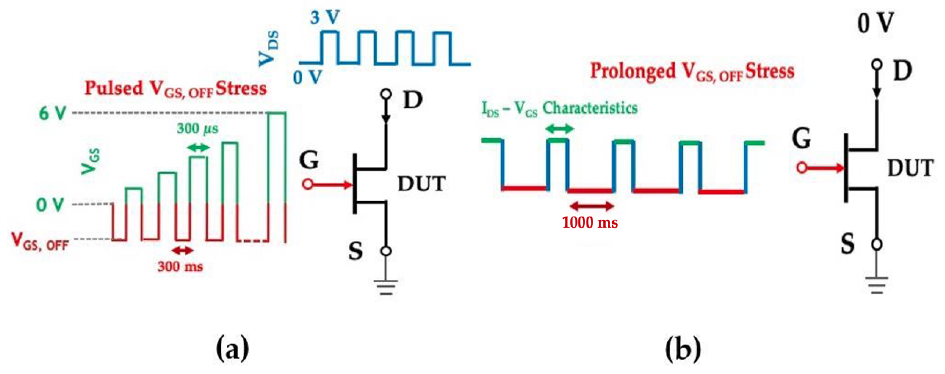
2. Experimental Details

A commercially available E-mode HEMT with p-GaN gate switches (200 V breakdown voltage) was used to investigate the dynamic instability and static reliability. The device under test (DUT) made up of AlGaN barrier layer, p-GaN layer, GaN transition layer, and a GaN buffer layer is shown in the schematic diagram of p-GaN gate HEMT in Figure 1. At present, we have studied the footprint of negative gate stress conditions through the device electrical parameters defined in the linear and saturation operating regions at VDS = 3 V. We focus our interest on the stability of VTH, increase of RDS-ON, degradation of Gm, max, and IGS-Leakage. A fresh device is used in this study to exhibit electrical characteristics, which includes output characteristics (IDS-VDS), transfer characteristics (IDS-VGS), and gate leakage characteristics (IGS-Leakage-VGS) before the negative gate (VGS) stress conditions, which are shown in Figure 2a,b. Thermally stable values of VTH = 1.6 V (observed at linear region of IDS = 0.05 A), RDS-ON = 25 mΩ (observed at saturation region of IDS, Max with VDS = 3 V and VGS = 6 V), Gm, max =1.5 S (defined at VDS = 3 V) and IGS, Leakage versus VGS characteristics (observed at VDS = 3 V and VGS from 0 V to 6 V) are confirmed with the data sheet. Further, fresh devices are put through to an extensive study of trapping or detrapping effect analysis under negative VGS bias stress at room temperature. All double-pulsed and prolonged VGS bias stress experiments were done with the Keithley 2651 A and 2601 A source meter systems.
In the pulsed negative VGS bias stress experiment, we studied the effect of pulsed negative gate bias stress conditions from the device parameter instability and degradation. A double pulse experiment technique was explored and used in the pulsed negative VGS bias stress experiment [32,33]. Device electrical parameters, such as VTH shift, IDS, Max or RDS-ON degradation, IGS-Leakage increase, and Gm, max, were investigated under pulsed VGS bias stress through two regimes of stress conditions. In the first regime, the influence of low pulsed VGS stress on the device electrical parameters of the DUT was obtained, where the pulsed stress VGS bias = −1 to −3 V and VDS = 3 V at room temperature. At the another regime, an increase in mid/high-stress voltages is studied for DUT, where the pulsed VGS bias stress = −5 V to −30 V and VDS = 3 V at room temperature. The reason for the large or harsh negative gate bias stress experiments is to observe the gate terminal stability level and variations in degradation phenomena of the device. Using a double pulse technique for each negative VGS pulse on DUT, the device stressed at Off-State for 300 ms and the on-state VGS pulse given for 300 μs. During each negative VGS bias pulse, both drain and source terminals are grounded with VDS = 0 V. The waveform for pulsed negative VGS bias stress experiments on the p-GaN gate HEMT device is shown in the Figure 3a.
In the prolonged negative VGS bias stress experiment, the stress time (tstress) of mid/high stress voltages was increased to observe device instability and degradation [34]. The negative gate bias instability on the E-mode GaN with p-GaN device at room temperature was studied. Under prolonged negative VGS bias stress, both the drain and source terminals are grounded with VDS = 0 V. From the studies of pulsed VGS stress experiment, the device is selectively subjected to the mid/high VGS bias stress from −10 V to −20 V. From the literature, under high negative gate bias stress, GaN-based powered devices have shown significant variation in degradation phenomena as stress voltage increases [28,34]. Based on previous studies, in this experiment the devices are subjected and studied with high stress voltage to ensure the gate terminal withstandability and degradation phenomena under harsh stress conditions. As we show below, for a harsh stress condition (such as −20 V), there is non-recoverable damage at room temperature after stress compared to low/mid stress conditions. For each prolonged negative VGS bias stress, different devices are used. Similar to the pulsed VGS stress experiment, the device initially characterized for fresh/virgin transfer characteristics with VDS = 3 V. Further, the device was subjected to VGS bias stress for 10,000 s. During the DUT stress phase, transfer characteristics were obtained at every 1000 s interval to extract VTH shift, IDS, Max or RDS-ON degradation, Gm, max degradation, and IGS-Leakage characteristics. The waveform for prolonged negative VGS bias stress experiments on the E-mode GaN power HEMT device is shown in Figure 3b.

3. Results and Discussion

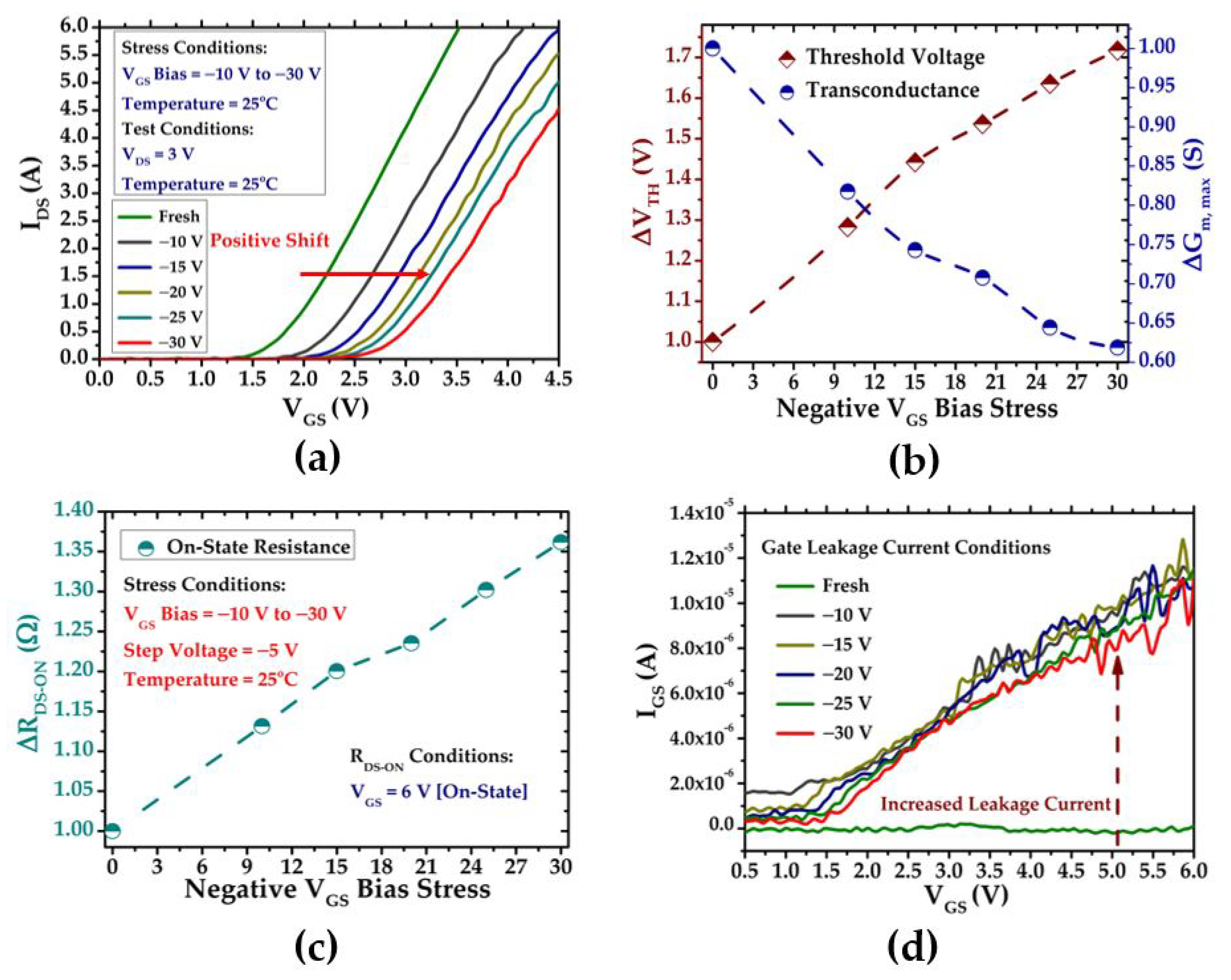
3.1. Degradation of Electrical Parameters under Pulsed VGS Bias Stress

Figure 4a shows the extracted △VTH and △Gm, max for different pulsed negative VGS bias stress (VGS bias = −1 V to −5 V & VDS = 3 V, room temperature) according to the preliminary data sheet standards. △RDS-ON and IGS-Leakage were extracted and shown in Figure 4b. The degradation parameters △VTH, △Gm, max, and △RDS-ON are normalized values of VTH, Gm, max, and RDS-ON (defined at VTH stress/VTH fresh), respectively. The transfer characteristics curve shifts in the positive direction with minimal significance under the low-voltage stress conditions, which results in an increase in the △VTH from 1 V to 1.11 V with respect to change in stress voltage. At the same time, the △Gm, max of the device decreases from 1 S to 0.90 S and △RDS-ON increases from 1 Ω to 1.04 Ω. Overall, the p-GaN gate HEMT, under the low stress voltage condition, show negligible and easily recoverable degradation at room temperature.
In parallel, the impact of high negative pulsed VGS bias stress (VGS Bias = −10 to −30 V and VDS = 3 V at room temperature), investigated through the transfer curve characteristics, is shown in Figure 5a. Further, the extracted △VTH and △Gm, max under constant voltage (VDS = 3 V) is shown in Figure 5b. The transfer characteristics curve shows the shifts towards positive direction quickly for the increase in negative VGS bias stress, and the normalized △VTH shift from 1 V to 1.71 V. From Figure 5b, the normalized △Gm, max degrades rapidly from 1 S to 0.61 S after the increase in stress. In general, the VTH of p-GaN gate HEMT device varies based on the inflow of holes from the JSchottky (Schottky junction) to outflow of holes through PN junction (p-GaN/2DEG). Therefore, the VTH shift obtained due to the trapping effect is close to the gate region for the VGS bias stress. In addition, Figure 5c shows the variation of △RDS-ON under high stress conditions, which is extracted at VGS = 6 V (On-State). The conductivity of the device decreases very rapidly with increase in negative stress voltage, whereas the normalized △RDS-ON increases from 1 Ω to 1.36 Ω after −30 V stress. Usually, the degradation of the RDS-ON could be caused by influence of traps in the gate region. It can be addressed that the dynamic trapping or detrapping process takes place in the gate channel region under negative VGS bias stress which causes the increases in RDS-ON with the shift of VTH. Figure 5d shows the gate leakage current characteristics of the device were studied with different negative VGS bias stress (VGS bias = −10 V to −30 V and VDS = 3 V at room temperature). Up to VGS = 1.5 V, the IGS-Leakage is very minimal and negligible. Moreover, the gate leakage current increases slightly for each step gate voltage under the device’s semi-on- and on-state.

3.2. Influence of Stress Time Evolution on Negative VGS Bias Stresses

The gate stress investigations show the influences of the mentioned instability and degradation of the device on the designers, which could directly affect the reliability of the system. At this experiment, the impact of various negative VGS bias stresses with respect to stress time evolution was investigated. Usually, the high negative gate bias stress (VGS bias = −10 V, −15 V, and −20 V) phases are not carried always in the most of the systems. However, these high values of gate bias stress show a notable effect on the device degradation and stability due to the trapping or detrapping task, which needs to be studied.
Figure 6a,b shows the extracted normalized △VTH shift and recovery, and Figure 6c,d shows the extracted normalized △RDS-ON degradation and recovery. The instability of VTH and degradation of RDS-ON are very minimal and fully recoverable at −5 V stress conditions. Further, these two electrical parameters are shown to be increasing as the magnitude of negative VGS bias stress increases. However, with increasing stress time, the device shows a gradual increase in △RDS-ON and the saturation of VTH degradation at each stress bias. In this, the △VTH initially shows the strong increase from 1 V to 1.6 V after 103 s stress and further increased minimal from 1.6 V to 1.98 V after 103 s to 104 s stress under a −20 V stress condition. The rapid increase in VTH at beginning shows the device’s strong dependence on stress voltage over stress time. At such a high stress voltage condition, the device does not show full recovery under room temperature compared to other stress voltage conditions. Similarly, the conductivity of the device is strongly affected by high stress condition, whereas the △RDS-ON increased from 1 Ω to 2.17 Ω within 104 s of stress. The △RDS-ON of the device shows full recovery under room temperature, which is shown in Figure 6d. The influence of stress time evolution on the gate leakage characteristics under mid/high prolonged negative VGS bias stresses is shown in the Figure 7a. Figure 7b shows the influence of stress voltage on IGS-Leakage versus gate bias with VDS = 3 V at room temperature. The gate current leakage over stress time for various stress voltages reveals that the IGS-Leakage has no changes with respect to increase in stress time. Further, a very minimal and negligible increase in the IGS-Leakage versus gate bias for various stress voltages is shown in Figure 7b. The pulsed negative VGS bias stress shows the strong impact on the device IGS-Leakage compared to the prolonged stress conditions.

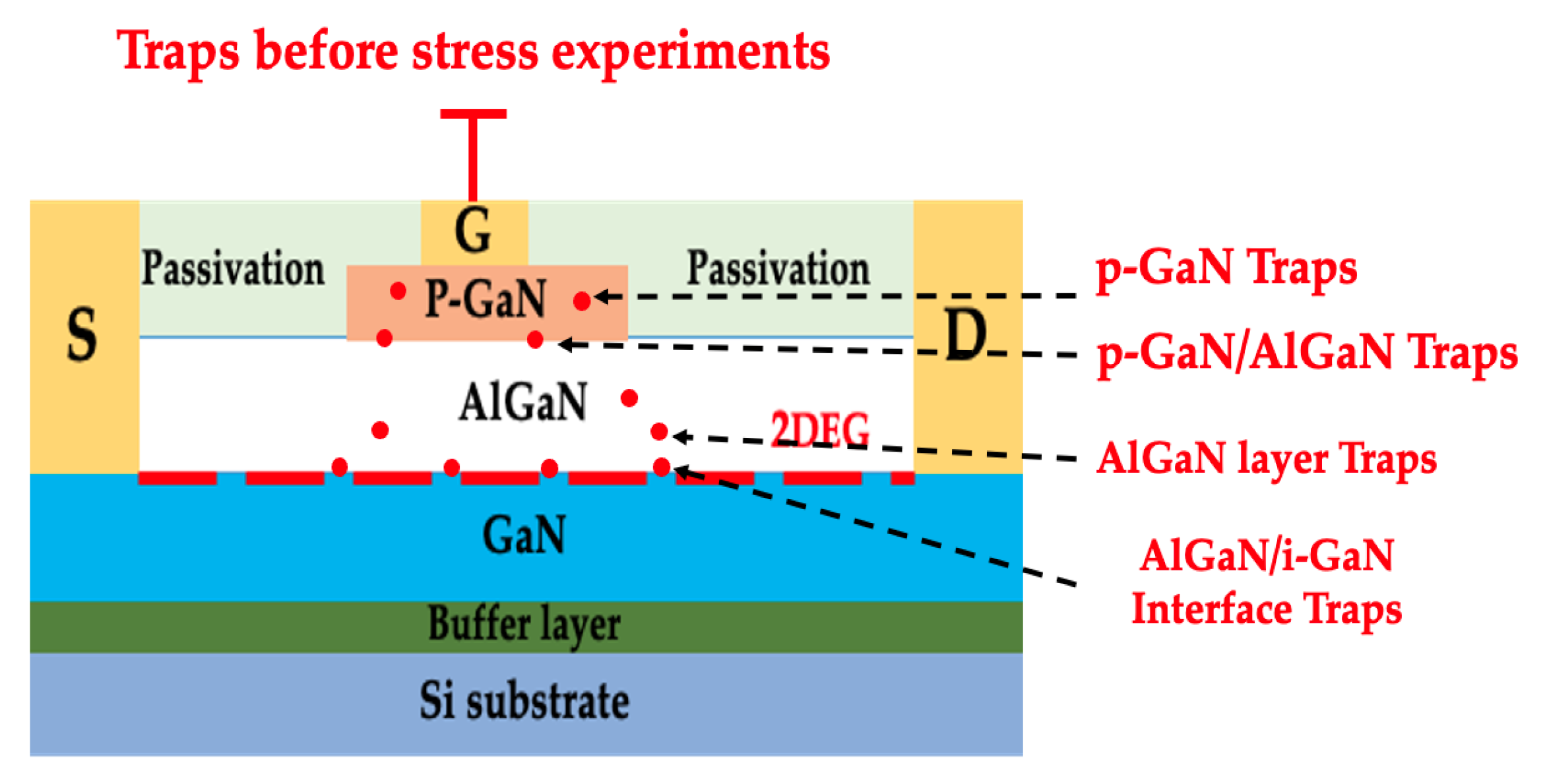
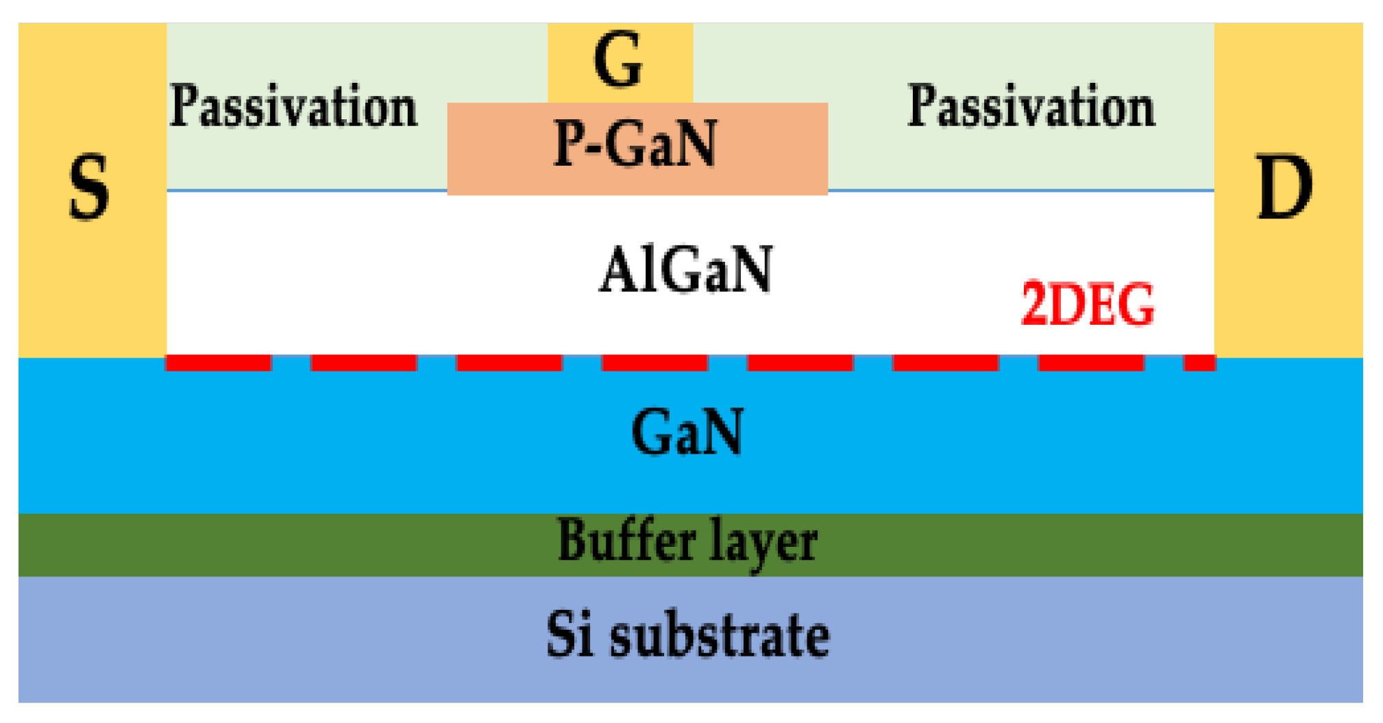
3.3. Influenced Degradation Mechanism and Analyzations

The GaN-based HEMT device holds several kinds of traps, which exist in the p-GaN region, the AlGaN barrier layer of the device, and the hetero-structure interface [35,36], such as Ga vacancy (VGa), Ga-N divacancy (VGa-VN) or oxygen impurity centers (ON), gallium antisite (NGa), or N vacancy (VN) [37]. Figure 8 shows the schematic p-GaN gate HEMT device diagram with trap states before stress conditions. According to the degraded electrical parameters under the negative VGS bias stress conditions in the p-GaN gate device, the degradation mechanisms are significantly influenced by trapping process under the gate region. The keen degradation and instabilities of electrical parameters under negative gate bias stress take place at room temperature, which could to be caused by hole deficiency and p-GaN/AlGAN interface traps. Therefore, the p-GaN gate-modeled HEMT structure is further subjected to in detail investigation for the above-mentioned device degradation mechanisms.
The physical mechanism behind the degradation effects for pulsed and prolonged VGS bias stress on the p-GaN gate HEMT is explained in the Figure 9a,b. In view of the Schottky gate contact of the studied device, where the metal/p-GaN hetero-structure acts as Schottky junction diode and the p-GaN/AlGaN/GaN structure acts as p-i-n junction diode, and respective junction capacitances [38,39]. Under negative gate bias, the JSchottky is forward biased, with small voltage drop on it. The p-i-n junction has reverse bias under negative gate bias stress, and all the voltage drops on the p-i-n junction (p-GaN/AlGaN/GaN). A small depletion takes place under stress conditions, where p-GaN is nearby the barrier layer AlGaN. As a result, the removal of holes flows from the depletion region in p-GaN to the gate region, and the p-i-n junction capacitor is charged which is shown in Figure 9a. Some of the donor-type holes at the p-GaN/AlGaN interface trao state also released under this charge process. When the gate bias switched to the positive level, the reduced charges at the p-GaN and interface of p-GaN/AlGaN are not immediately restored, which plays a strong role in the positive shift of threshold voltage (VTH), increase of on-state resistance (RDS-ON), and degradation of transconductance (Gm, max). As the magnitude of stress voltage is increased, the high order of hole deficiency takes place in the strong instability and degradations. As the stress time increases, the formation of the built-in electric potential by ionizing the donor-type holes will reduce the holes’ deficiency from the trap state, which leads to the saturation of the VTH shift degradation degree. Under the negative gate bias stress condition, the release of donor type holes from the p-GaN/AlGaN interface trap state by the reverse biased p-i-n junction capacitor charge process is not modulated due to the lack of an electron injection or recombination process under VGS stress bias. Meanwhile, the acceptor-like traps at the AlGaN/i-GaN interface and the buffer layer are also very difficult to activate as the electric potential is very low at buffer layer and the drain bias is zero during negative gate bias stress. At this point, detrapping the activated donor-type traps from the interface (p-GaN/AlGaN) and holes from gate region could primarily influence the electrical parameters degradation and instabilities. If the gate bias increases more negative, the number of released holes from the p-GaN and p-GaN/AlGaN trap state will be increased, which results in more significant degradations and instabilities. This agrees with the results shown in both pulsed and prolonged negative gate bias stress experiment as shown in the Figure 5 and Figure 6.

4. Conclusions

In summary, we have investigated the static electrical performances of E-mode GaN HEMTs with p-GaN gate under negative VGS bias stresses as well as the physics-based mechanism behind the device degradation. The existence holes trapping at the gate region can play a role in the positive shift of the VTH, increase of the RDS-ON, decrease of the Gm, max, and the increase of the IGS-Leakage. Under prolonged negative VGS bias stress, the ionization of donor-type holes occurs at the p-GaN/AlGaN interface trap state, which results in a saturation of the degree of VTH positive shift over the stress time evolution. Meanwhile, the on-state resistance under prolonged stress simultaneously increases with evolution of both the magnitude of the stress voltage and stress time. The extracted values for both pulsed and prolonged stress experiments show great agreement with the dominant degradation mechanisms. To achieve long-term system stability and reliability, more attention needs to be paid to the importance of electrical degradation, which is affected by a negative gate bias stress condition. This paper gives an understanding of the E-mode GaN HEMT with p-GaN gate devices, static reliability, and dynamic instability issues for system designers to avoid unsuitable negative bias conditions.

Author Contributions

Conceptualization, methodology, formal analysis, investigation, data curation, and writing—original draft preparation, S.E.; writing—review and editing, validation, supervision, funding acquisition, and project administration, S.C.; visualization and resources E.Y.C. All authors have read and agreed to the published version manuscript.

Funding

This research received no external funding.

Institutional Review Board Statement

Not applicable.

Informed Consent Statement

Not applicable.

Data Availability Statement

The data presented in this study are available on request from the corresponding author.

Conflicts of Interest

The authors declare no conflict of interest.

References

  1. Mishra, U.K.; Shen, L.; Kazior, T.E.; Wu, Y.F. GaN-based RF power devices and amplifiers. Proc. IEEE 2008, 96, 287–305. [Google Scholar] [CrossRef]
  2. Tang, Y.; Shinohara, K.; Regan, D.; Corrion, A.; Brown, D.; Wong, J.; Schmitz, A.; Fung, H.; Kim, S.; Micovic, M. Ultrahigh-speed GaN high-electron-mobility transistors with fT/fmax of 454/444 GHz. IEEE Electron Device Lett. 2015, 36, 549–551. [Google Scholar] [CrossRef]
  3. Wu, Y.F.; Moore, M.; Saxler, A.; Wisleder, T.; Parikh, P. 40-W/mm double field-plated GaN HEMTs. In Proceedings of the 2006 64th Device Research Conference, State College, PA, USA, 26–28 June 2006; pp. 151–152. [Google Scholar]
  4. Lu, B.; Palacios, T. High Breakdown (>1500 V) AlGaN/GaN HEMTs by Substrate-Transfer Technology. IEEE Electron Device Lett. 2010, 31, 951–953. [Google Scholar] [CrossRef]
  5. Pengelly, R.S.; Wood, S.M.; Milligan, J.W.; Sheppard, S.T.; Pribble, W.L. A review of GaN on SiC high electron-mobility power transistors and MMICs. IEEE Trans. Microw. Theory Tech. 2012, 60, 1764–1783. [Google Scholar] [CrossRef]
  6. Oeder, T.; Castellazzi, A.; Pfost, M. Experimental study of the short-circuit performance for a 600V normally-off p-gate GaN HEMT. In Proceedings of the 2017 29th International Symposium on Power Semiconductor Devices and IC’s (ISPSD), Sapporo, Japan, 28 May–1 June 2017; pp. 211–214. [Google Scholar]
  7. Li, H.; Li, X.; Wang, X.; Lyu, X.; Cai, H.; Alsmadi, Y.M.; Liu, L.; Bala, S.; Wang, J. Robustness of 650-V enhancement-mode GaN HEMTs under various short-circuit conditions. IEEE Trans. Ind. Appl. 2018, 55, 1807–1816. [Google Scholar] [CrossRef]
  8. Fernández, M.; Perpiñá, X.; Vellvehi, M.; Jorda, X.; Roig, J.; Bauwens, F.; Tack, M. Short-circuit capability in p-GaN HEMTs and GaN MISHEMTs. In Proceedings of the 2017 29th International Symposium on Power Semiconductor Devices and IC’s (ISPSD), Sapporo, Japan, 28 May–1 June 2017; pp. 455–458. [Google Scholar]
  9. Fernández, M.; Perpiñà, X.; Roig, J.; Vellvehi, M.; Bauwens, F.; Jordà, X.; Tack, M. P-GaN HEMTs drain and gate current analysis under short-circuit. IEEE Electron Device Lett. 2017, 38, 505–508. [Google Scholar] [CrossRef]
  10. Del Alamo, J.A.; Joh, J. GaN HEMT reliability. Microelectron. Reliab. 2009, 49, 1200–1206. [Google Scholar] [CrossRef]
  11. Meneghini, M.; Rossetto, I.; Rizzato, V.; Stoffels, S.; Van Hove, M.; Posthuma, N.; Wu, T.L.; Marcon, D.; Decoutere, S.; Meneghesso, G.; et al. Gate stability of GaN-based HEMTs with p-type gate. Electronics 2016, 5, 14. [Google Scholar] [CrossRef]
  12. Wu, T.L.; Marcon, D.; De Jaeger, B.; Van Hove, M.; Bakeroot, B.; Lin, D.; Stoffels, S.; Kang, X.; Roelofs, R.; Groeseneken, G.; et al. The impact of the gate dielectric quality in developing Au-free D-mode and E-mode recessed gate AlGaN/GaN transistors on a 200mm Si substrate. In Proceedings of the 2015 IEEE 27th International Symposium on Power Semiconductor Devices & IC’s (ISPSD), Hong Kong, China, 10–14 May 2015; pp. 225–228. [Google Scholar]
  13. Huang, X.; Liu, Z.; Li, Q.; Lee, F.C. Evaluation and application of 600 V GaN HEMT in cascode structure. IEEE Trans. Power Electron. 2013, 29, 2453–2461. [Google Scholar] [CrossRef]
  14. Chen, S.H.; Chou, P.C.; Cheng, S. Evaluation of thermal performance of packaged GaN HEMT cascode power switch by transient thermal testing. Appl. Therm. Eng. 2016, 98, 1003–1012. [Google Scholar] [CrossRef]
  15. Wu, C.H.; Han, P.C.; Liu, S.C.; Hsieh, T.E.; Lumbantoruan, F.J.; Ho, Y.H.; Chen, J.Y.; Yang, K.S.; Wang, H.C.; Lin, Y.K.; et al. High-performance normally-OFF GaN MIS-HEMTs using hybrid ferroelectric charge trap gate stack (FEG-HEMT) for power device applications. IEEE Electron Device Lett. 2018, 39, 991–994. [Google Scholar] [CrossRef]
  16. Hung, T.H.; Park, P.S.; Krishnamoorthy, S.; Nath, D.N.; Rajan, S. Interface charge engineering for enhancement-mode GaN MISHEMTs. IEEE Electron Device Lett. 2014, 35, 312–314. [Google Scholar] [CrossRef]
  17. Uemoto, Y.; Hikita, M.; Ueno, H.; Matsuo, H.; Ishida, H.; Yanagihara, M.; Ueda, T.; Tanaka, T.; Ueda, D. Gate injection transistor (GIT)—A normally-off AlGaN/GaN power transistor using conductivity modulation. IEEE Trans. Electron Devices 2007, 54, 3393–3399. [Google Scholar] [CrossRef]
  18. Zanandrea, A.; Bahat-Treidel, E.; Rampazzo, F.; Stocco, A.; Meneghini, M.; Zanoni, E.; Hilt, O.; Ivo, P.; Wuerfl, J.; Meneghesso, G. Single-and double-heterostructure GaN-HEMTs devices for power switching applications. Microelectron. Reliab. 2012, 52, 2426–2430. [Google Scholar] [CrossRef]
  19. Moens, P.; Vanmeerbeek, P.; Banerjee, A.; Guo, J.; Liu, C.; Coppens, P.; Salih, A.; Tack, M.; Caesar, M.; Uren, M.; et al. On the impact of carbon-doping on the dynamic Ron and off-state leakage current of 650V GaN power devices. In Proceedings of the 2015 IEEE 27th International Symposium on Power Semiconductor Devices & IC’s (ISPSD), Hong Kong, China, 10–14 May 2015; pp. 37–40. [Google Scholar]
  20. Mahajan, D.; Khandelwal, S. Impact of p-GaN layer doping on switching performance of enhancement mode GaN devices. In Proceedings of the 2018 IEEE 19th Workshop on Control and Modeling for Power Electronics (COMPEL), Padua, Italy, 25–28 June 2018; pp. 1–4. [Google Scholar]
  21. He, J.; Tang, G.; Chen, K.J. VTH Instability of p-GaN Gate HEMTs Under Static and Dynamic Gate Stress. IEEE Electron Device Lett. 2018, 39, 1576–1579. [Google Scholar]
  22. Efthymiou, L.; Murukesan, K.; Longobardi, G.; Udrea, F.; Shibib, A.; Terrill, K. Understanding the threshold voltage instability during OFF-state stress in p-GaN HEMTs. IEEE Electron Device Lett. 2019, 40, 1253–1256. [Google Scholar] [CrossRef]
  23. Wang, H.; Xie, R.; Liu, C.; Wei, J.; Tang, G.; Chen, K.J. Maximizing the performance of 650 V p-GaN gate HEMTs: Dynamic ron characterization and gate-drive design considerations. In Proceedings of the 2016 IEEE Energy Conversion Congress and Exposition (ECCE), Milwaukee, WI, USA, 18–22 September 2016; pp. 1–6. [Google Scholar]
  24. Vetury, R.; Zhang, N.Q.; Keller, S.; Mishra, U.K. The impact of surface states on the DC and RF characteristics of AlGaN/GaN HFETs. IEEE Trans. Electron Devices 2001, 48, 560–566. [Google Scholar] [CrossRef]
  25. Nguyen, C.; Nguyen, N.; Grider, D. Drain current compression in GaN MODFETs under large-signal modulation at microwave frequencies. Electron. Lett. 1999, 35, 1380–1382. [Google Scholar] [CrossRef]
  26. Chen, Y.; Feng, J.; Wang, J.; Xu, X.; He, Z.; Li, G.; Lei, D.; Chen, Y.; Huang, Y. Degradation behavior and mechanisms of E-mode GaN HEMTs with p-GaN gate under reverse electrostatic discharge stress. IEEE Trans. Electron Devices 2020, 67, 566–570. [Google Scholar] [CrossRef]
  27. Xu, X.; Li, B.; Chen, Y.; Wu, Z.; He, Z.; En, Y.; Huang, Y. Analysis of trap and recovery characteristics based on low-frequency noise for E-mode GaN HEMTs with p-GaN gate under repetitive short-circuit stress. J. Phys. D Appl. Phys. 2020, 53, 175101. [Google Scholar] [CrossRef]
  28. Guo, A.; del Alamo, J.A. Negative-bias temperature instability of GaN MOSFETs. In Proceedings of the 2016 IEEE International Reliability Physics Symposium (IRPS), Pasadena, CA, USA, 17–21 April 2016; pp. 4A-1-1–4A-1-6. [Google Scholar]
  29. Yen, C.T.; Hung, H.T.; Hung, C.C.; Lee, C.Y.; Lee, H.Y.; Lee, L.S.; Huang, Y.F.; Cheng, C.Y.; Chuang, P.J.; Hsu, F.J. Negative Bias Temperature Instability of SiC MOSFET. In Materials Science Forum; Trans Tech Publications Ltd.: Stafa-Zurich, Switzerland, 2016; Volume 858, pp. 595–598. [Google Scholar]
  30. Chen, J.; Hua, M.; Wei, J.; He, J.; Wang, C.; Zheng, Z.; Chen, K.J. OFF-state Drain-voltage-stress-induced VTH Instability in Schottky-type p-GaN Gate HEMTs. IEEE J. Emerg. Sel. Top. Power Electron. 2020. [Google Scholar] [CrossRef]
  31. Zhang, C.; Liu, S.; Li, S.; Li, N.; Tao, X.; Hou, B.; Zhou, B.; Wei, J.; Chen, Y.; Sun, W. Electrical performances degradations and physics based mechanisms under negative bias temperature instability stress for p-GaN gate high electron mobility transistors. Semicond. Sci. Technol. 2020, 36, 014007. [Google Scholar] [CrossRef]
  32. Elangovan, S.; Cheng, S.; Chang, E.Y. Reliability characterization of gallium nitride MIS-HEMT based cascode devices for power electronic applications. Energies 2020, 13, 2628. [Google Scholar] [CrossRef]
  33. Santarelli, A.; Cignani, R.; Gibiino, G.P.; Niessen, D.; Traverso, P.A.; Florian, C.; Schreurs, D.M.P.; Filicori, F. A double-pulse technique for the dynamic I/V characterization of GaN FETs. IEEE Microw. Wirel. Components Lett. 2013, 24, 132–134. [Google Scholar] [CrossRef]
  34. Guo, A.; del Alamo, J.A. Unified mechanism for positive-and negative-bias temperature instability in GaN MOSFETs. IEEE Trans. Electron Devices 2017, 64, 2142–2147. [Google Scholar] [CrossRef]
  35. Wu, T.L.; Marcon, D.; You, S.; Posthuma, N.; Bakeroot, B.; Stoffels, S.; Van Hove, M.; Groeseneken, G.; Decoutere, S. Forward bias gate breakdown mechanism in enhancement-mode p-GaN gate AlGaN/GaN high-electron mobility transistors. IEEE Electron Device Lett. 2015, 36, 1001–1003. [Google Scholar] [CrossRef]
  36. Chang, T.F.; Hsiao, T.C.; Huang, C.F.; Kuo, W.H.; Lin, S.F.; Samudra, G.S.; Liang, Y.C. Phenomenon of drain current instability on p-GaN gate AlGaN/GaN HEMTs. IEEE Trans. Electron Devices 2014, 62, 339–345. [Google Scholar] [CrossRef]
  37. Rossetto, I.; Meneghini, M.; Rizzato, V.; Ruzzarin, M.; Favaron, A.; Stoffels, S.; Van Hove, M.; Posthuma, N.; Wu, T.L.; Marcon, D.; et al. Study of the stability of e-mode GaN HEMTs with p-GaN gate based on combined DC and optical analysis. Microelectron. Reliab. 2016, 64, 547–551. [Google Scholar] [CrossRef]
  38. Li, S.; Liu, S.; Tian, Y.; Zhang, C.; Wei, J.; Tao, X.; Li, N.; Zhang, L.; Sun, W. High-temperature electrical performances and physics-based analysis of p-GaN HEMT device. IET Power Electron. 2019, 13, 420–425. [Google Scholar] [CrossRef]
  39. Ma, X.H.; Zhu, J.J.; Liao, X.Y.; Yue, T.; Chen, W.W.; Hao, Y. Quantitative characterization of interface traps in Al2O3/AlGaN/GaN metal-oxide-semiconductor high-electron-mobility transistors by dynamic capacitance dispersion technique. Appl. Phys. Lett. 2013, 103, 033510. [Google Scholar] [CrossRef]
Figure 1. Most favorable schematic cross section of the E-mode GaN High Electron Mobility Transistor (HEMT) with p-GaN gate.
Energies 14 02170 g001
Figure 2. Representative of commercialized 200 V E-mode GaN power HEMT switch fresh electrical characteristics at room temperature: (a) output characteristics and (b) transfer characteristics.
Energies 14 02170 g002
Figure 3. Schematic stress waveform of negative gate stress applied on E-mode GaN power HEMT with p-GaN device under test: (a) Pulsed Negative Gate Bias Stress and (b) Prolonged Negative Gate Bias Stress.
Energies 14 02170 g003
Figure 4. Extracted (a) △VTH and △Gm, max and (b) △RDS-ON and IGS-Leakage under low-voltage pulsed stress conditions.
Energies 14 02170 g004
Figure 5. (a) Extracted Transfer Characteristics of p-GaN HEMT, (b) extracted △Gm, max and △VTH, (c) extracted △RDS-ON and (d) IGS-Leakage under high voltage pulsed stress conditions.
Energies 14 02170 g005
Figure 6. Extracted (a) △VTH shift under stress conditions, (b) △VTH recovery under room temperature, (c) extracted △RDS-ON degradation under stress conditions, and (d) △RDS-ON recovery under room temperature.
Energies 14 02170 g006
Figure 7. The gate leakage characteristics of p-GaN gate HEMT as a function of (a) stress time and (b) stress voltages during prolonged negative VGS bias stress.
Energies 14 02170 g007
Figure 8. Schematic cross section of p-GaN HEMT device with traps in fresh device before stress conditions.
Energies 14 02170 g008
Figure 9. Band diagram of the p-GaN gate HEMT (a) device under negative gate bias stress condition and the (b) device after stress condition under turn-on state.
Energies 14 02170 g009
Publisher’s Note: MDPI stays neutral with regard to jurisdictional claims in published maps and institutional affiliations.

