
100 kW Three-Phase Wireless Charger for EV: Experimental Validation Adopting Opposition Method


Abstract
:1. Introduction
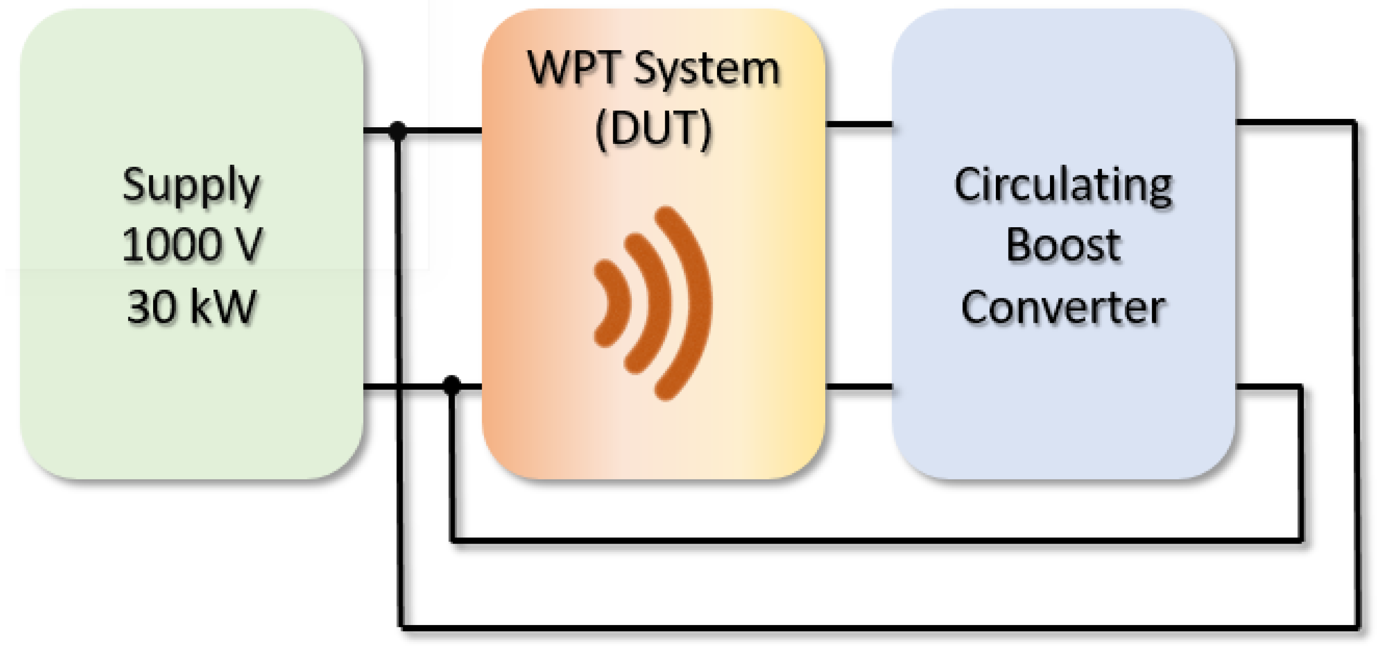
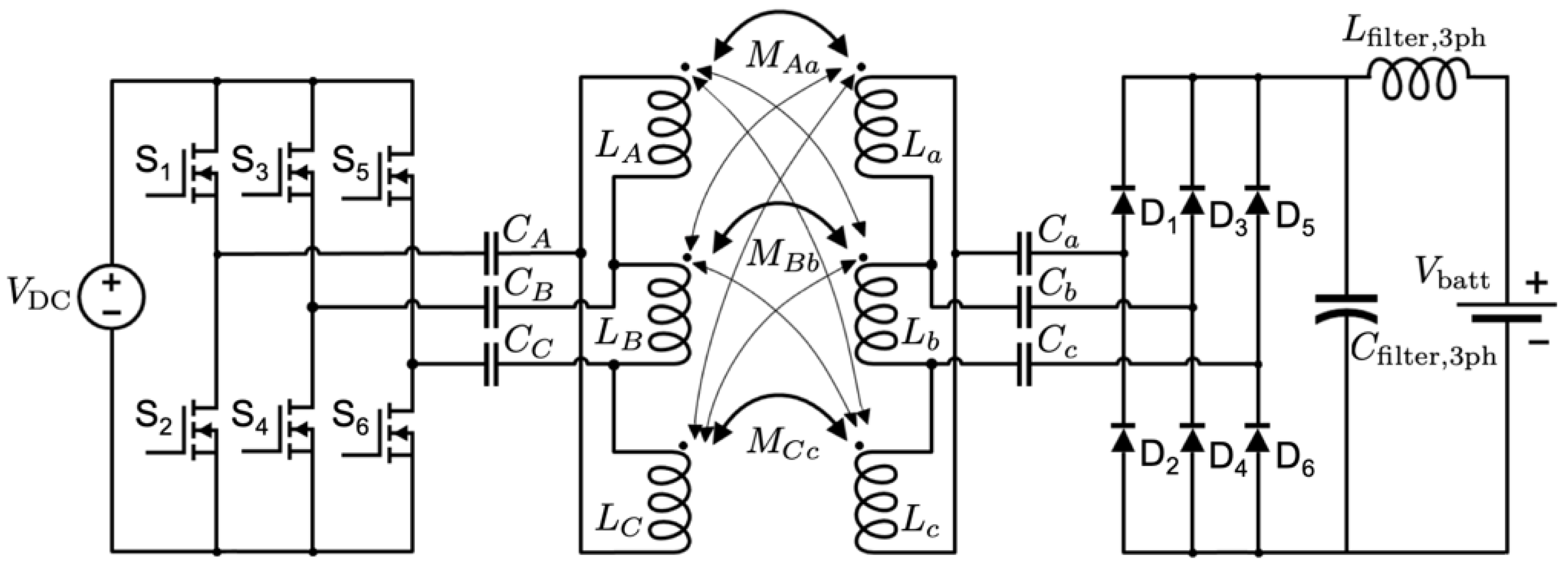
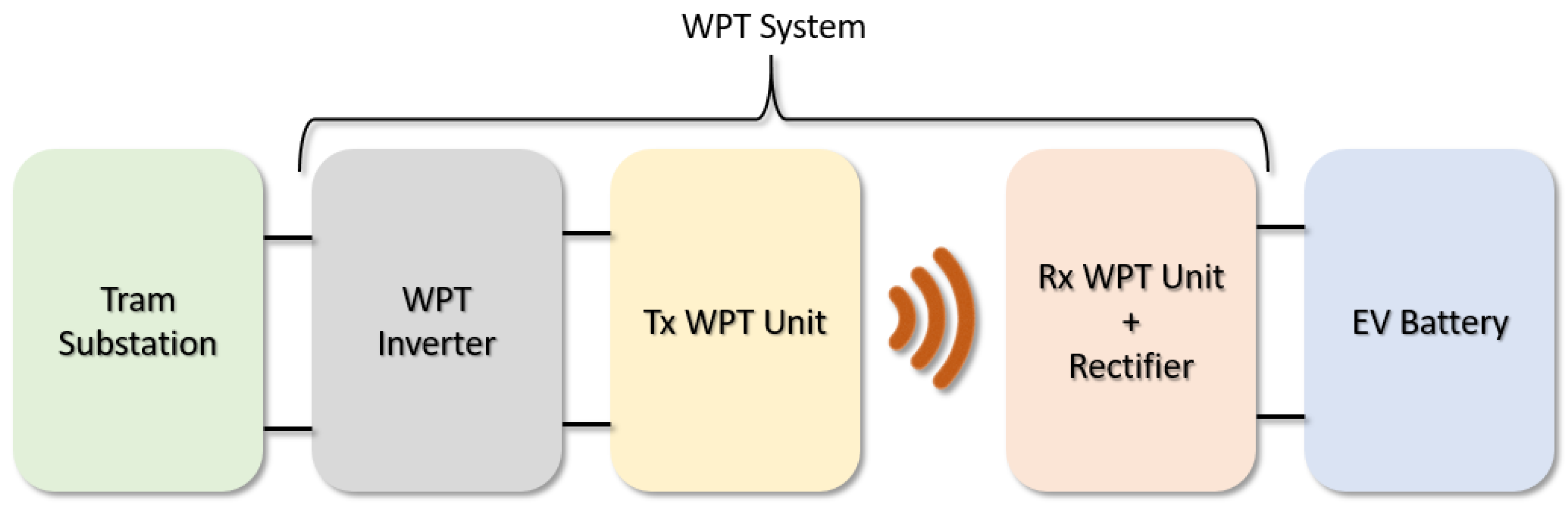
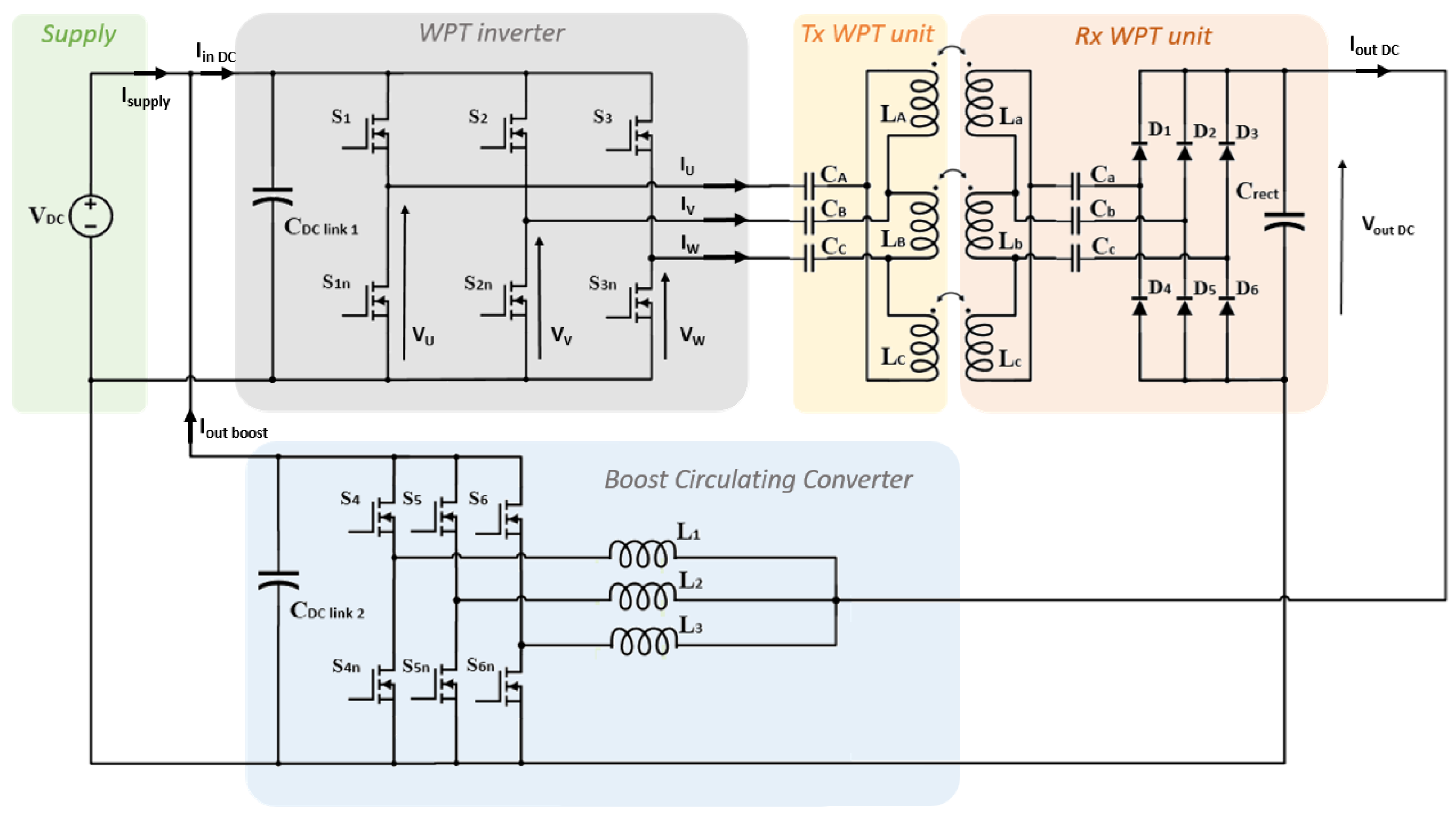
2. Charging Structure
3. System Modelling
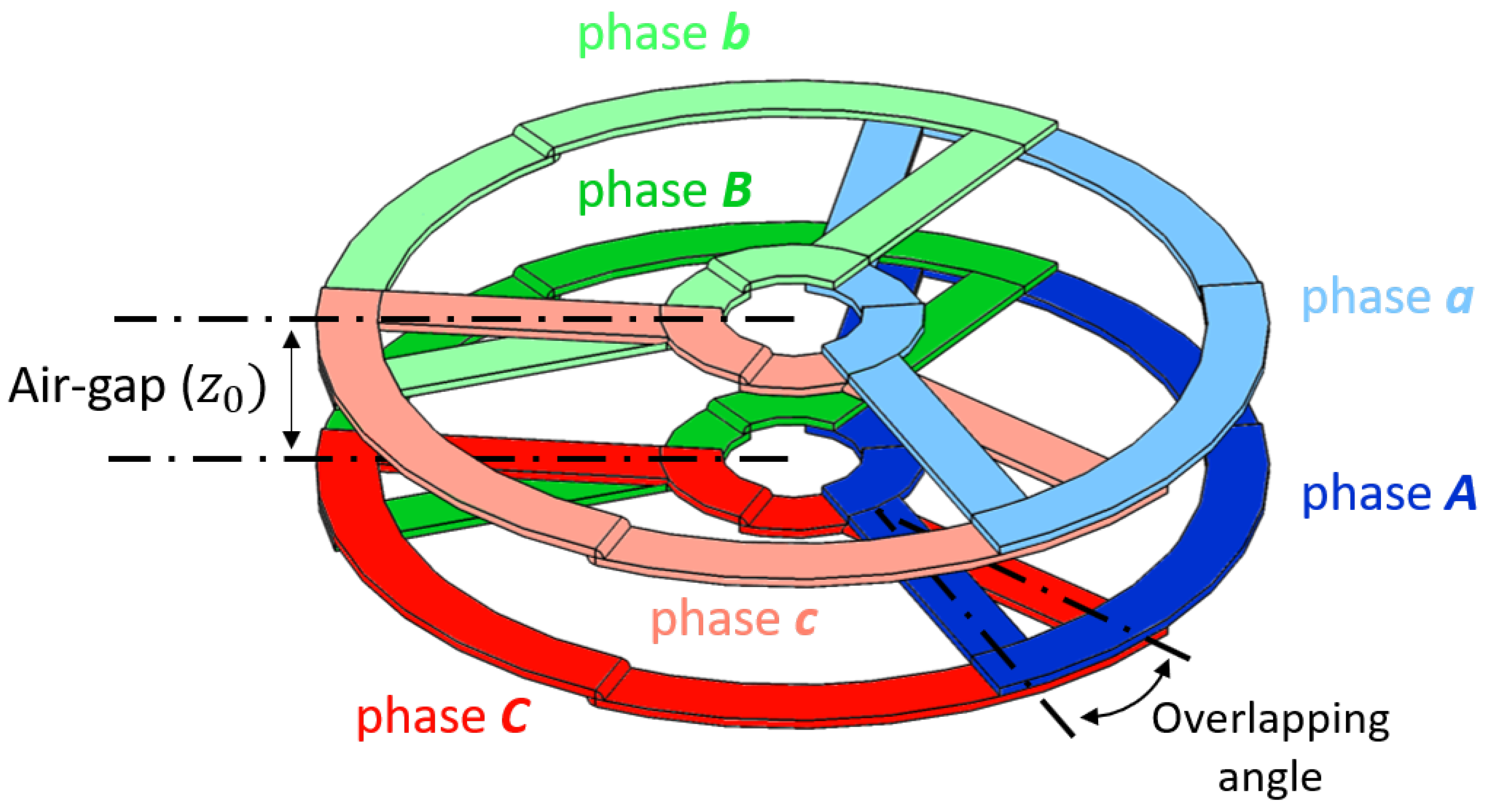
3.1. Electromagnetic Structure Description
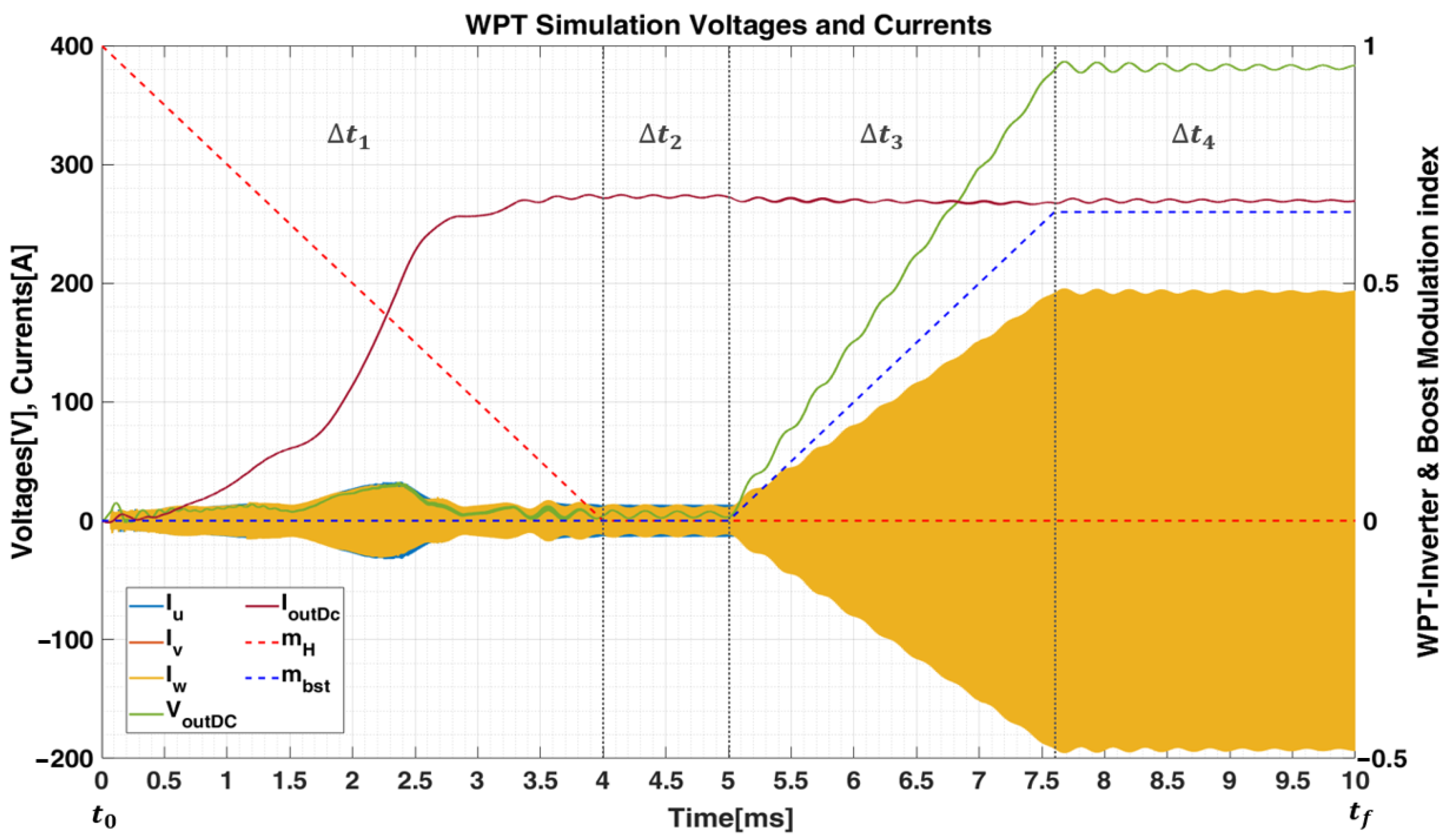
3.2. Control and Simulation Analysis
- At time , at the very beginning of the process, the system is at the starting condition. Considering the WPT inverter, it is possible to notice that the modulation depth is . In this condition, the TPP primary side can be considered to be an open circuit. At the same time, the boost converter has a modulation index or in another way can be considered to be an equivalent short circuit at the output of the WPT system. At the end of this state, all the bus capacitors are pre-charged and at a steady state.
- For , the modulation index of the WPT inverter increases, following a linear ramp variation, till reaches the value of . In this condition the output-phase voltages waveforms starting to be non-null till the end of the ramp, instant in which they reach the of pulse width. At the same time, the boost converter is forced to maintain the value of , still a short circuit see from diode bridge terminals. Within this status, the voltage at the battery side increases slightly due to the death time of the converter switches. However, side some more words are needed regarding the current evolution at the battery. In fact, replacing the AC physical dimensions with the corresponding DC Battery-side aspects in (2) and writing the DC current function of the other dimensions, the following relationship can be obtained:From (9) can be deduced that the current at DC output increases as the voltage at the primary side grows. The maximum is reached within at WPT inverter.
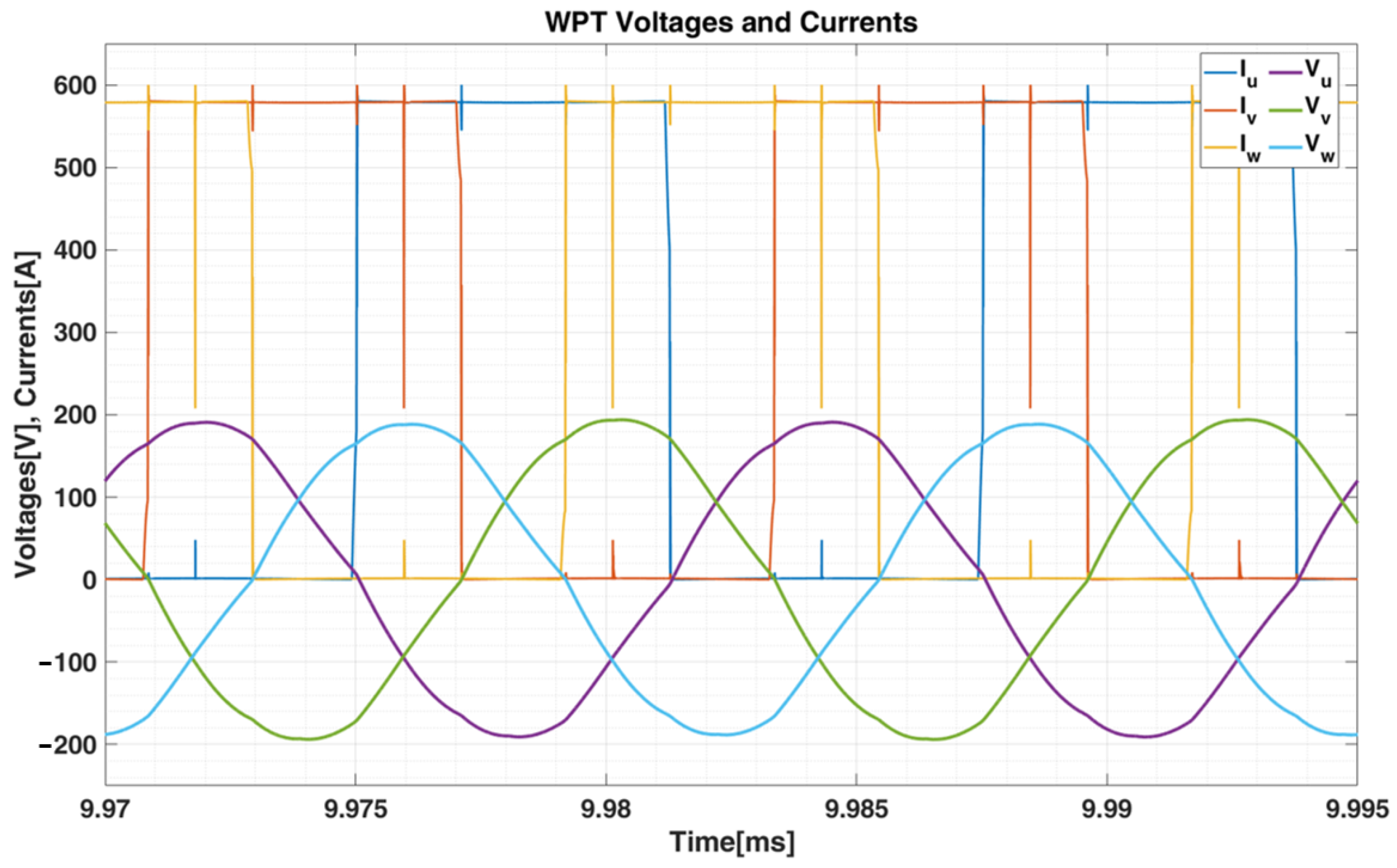
- For , the modulation depth of WPT inverter reached . Thus, the equivalent duty cycle is and the output-phase voltages become full square wave. In this condition, the boost remains still with and as a consequence the voltage at the battery side remains low, while the current reaches the maximum. This state has been introduced to obtain a steady-state at the primary side, where the phase currents and the voltages are in phase thanks to the resonance of the WPT system.
- For , the WPT inverter can be considered in steady state with modulation index . In this portion of the analysis the boost increases its modulation depth from , following a linear ramp variation, to reach at the terminals of diode bridge a final DC value of V. Considering now again the inductance model for the equivalent single-phase system [30], it is possible to rearrange the (2) highlighting the relationship between the output DC voltage and the input current of the electromagnetic system as:From the (10) it is clear that if the output voltage on the battery side increases, the current at the primary side grows too.
- For , the boost converter reaches the final value for its modulation index (i.e., ) which corresponds to the final value of the DC voltage at battery side V. From (9) the DC after the diode bridge remains the same because of the full square wave at the primary side. However, the output current of the WPT inverter, thanks to (10) reaches a steady-state, as can be seen from Figure 7 due to the constant output voltage at the battery side. This is the final steady-state of the analysis. The output DC voltage and current reach the target values equivalent to a State-Of-Charge (SOC ) of EV battery charge. In the fast-charging process, in fact, the charge will stop after having reached this SoC level.
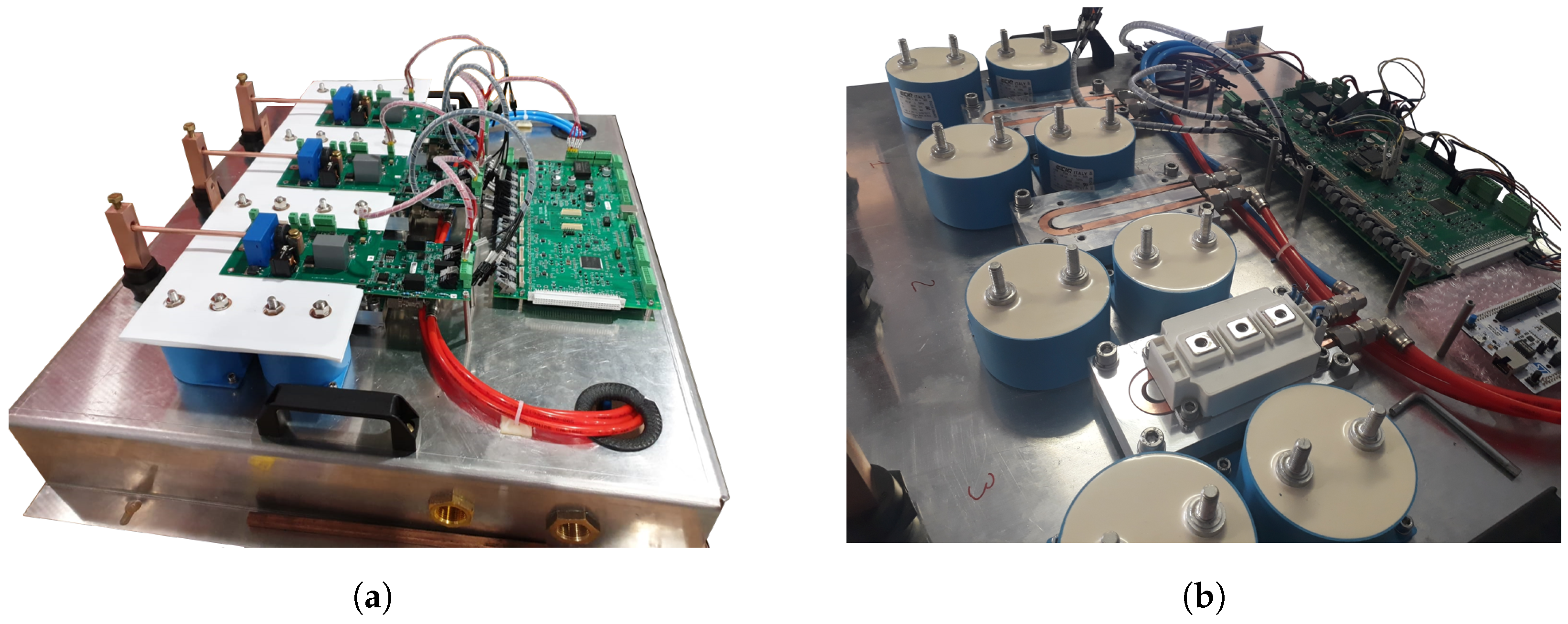
4. Prototype System
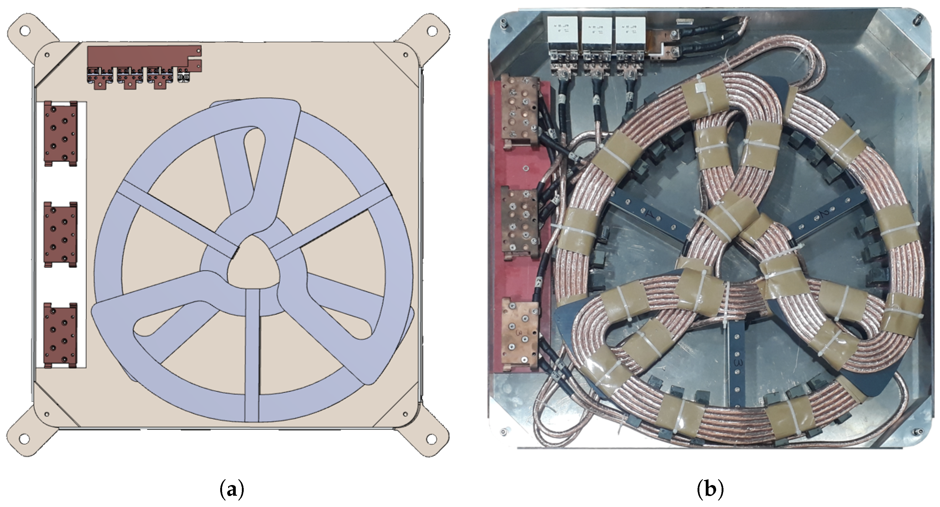
4.1. WPT Unit Realization
4.2. Converter Design
5. Experimental Validation
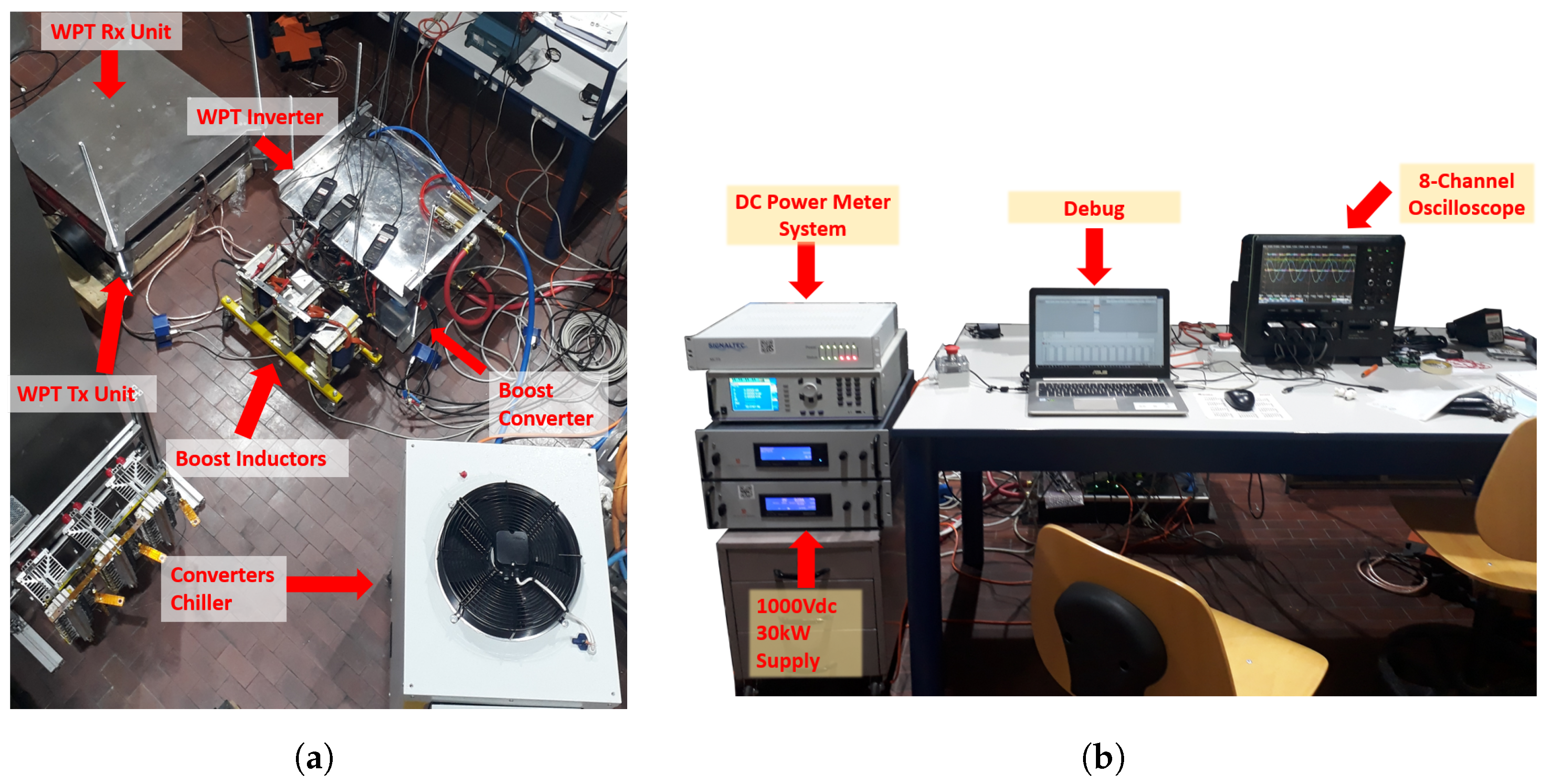
5.1. Experimental Setup
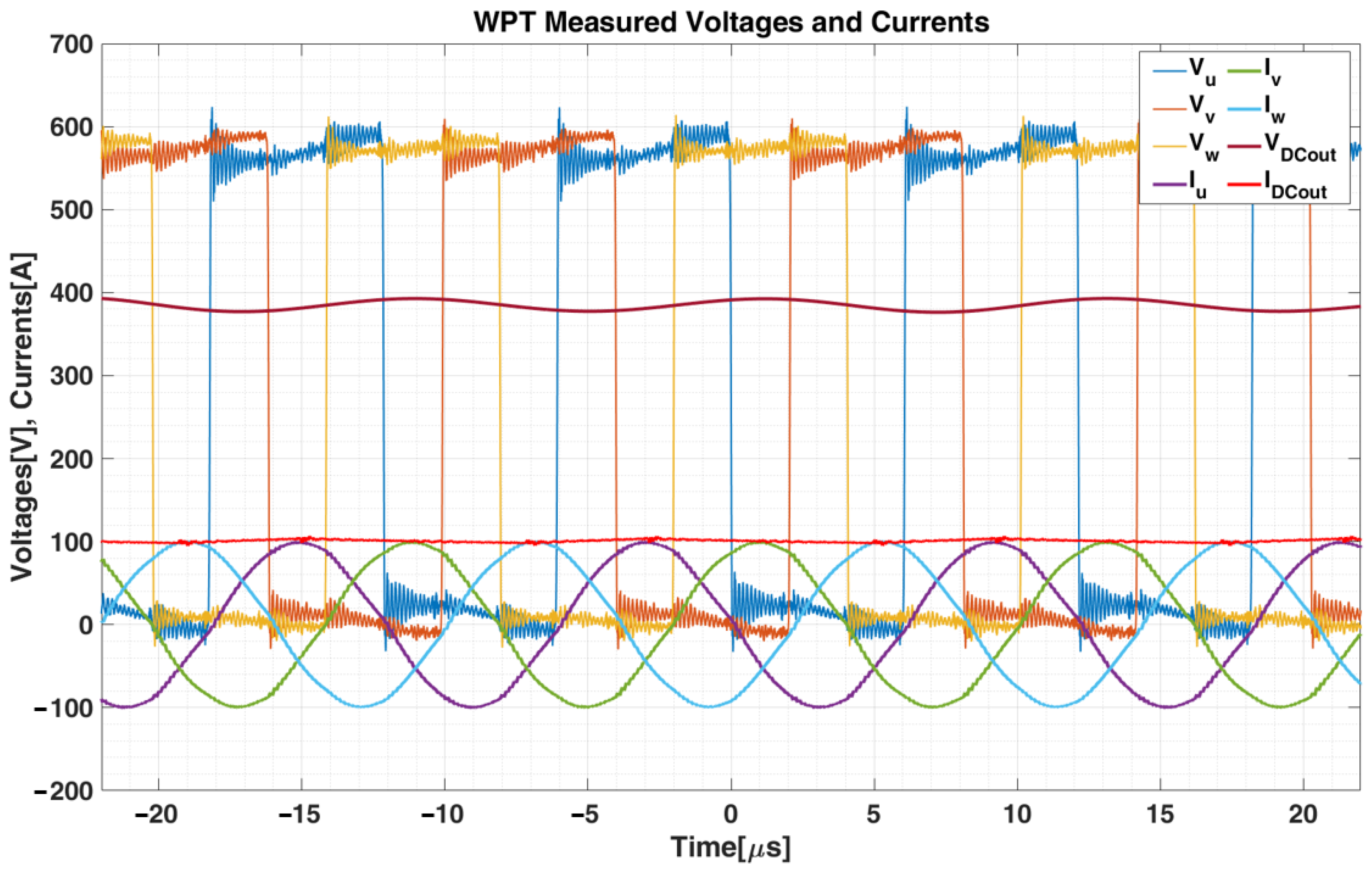
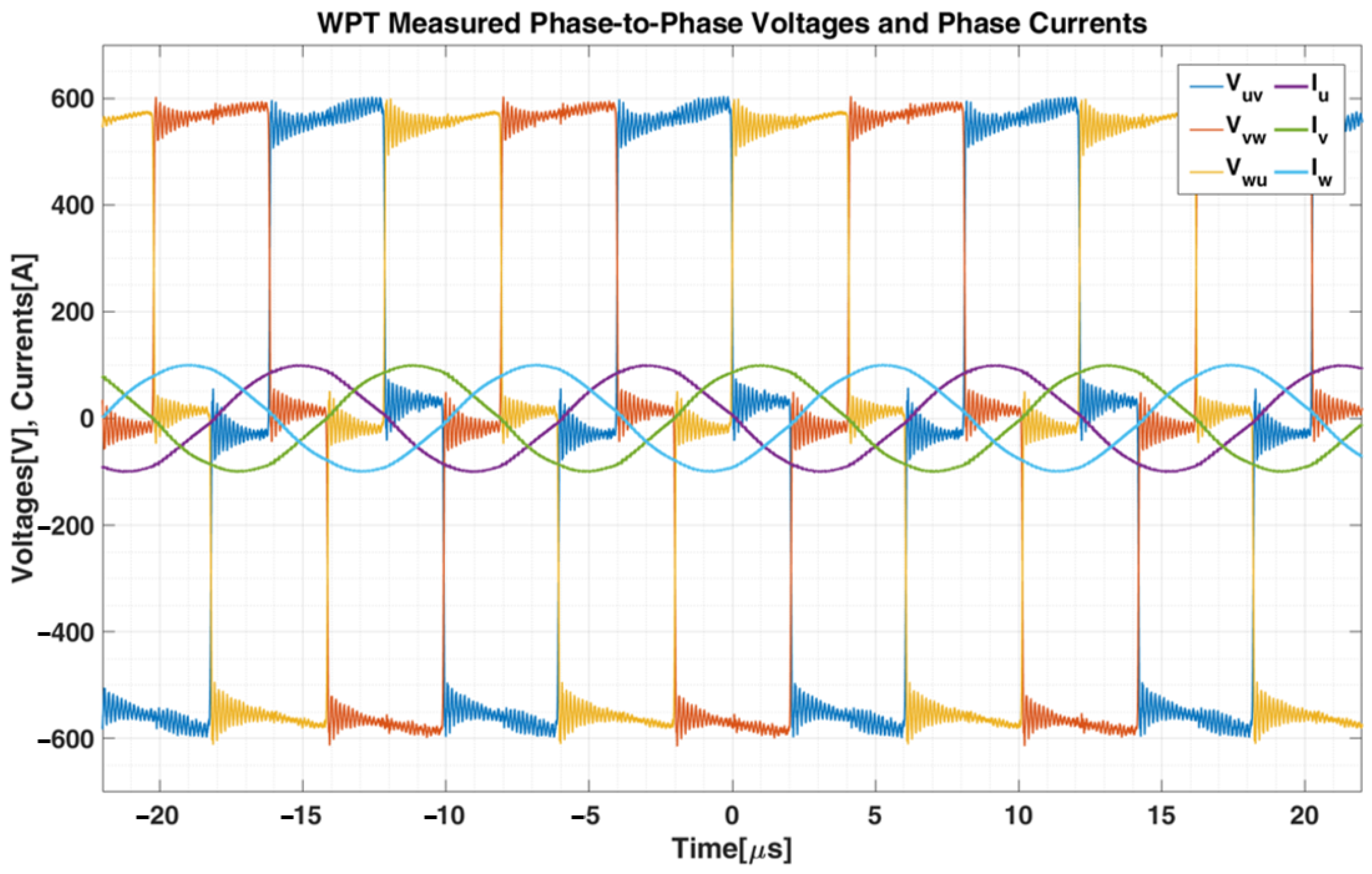
5.2. Experimental Results
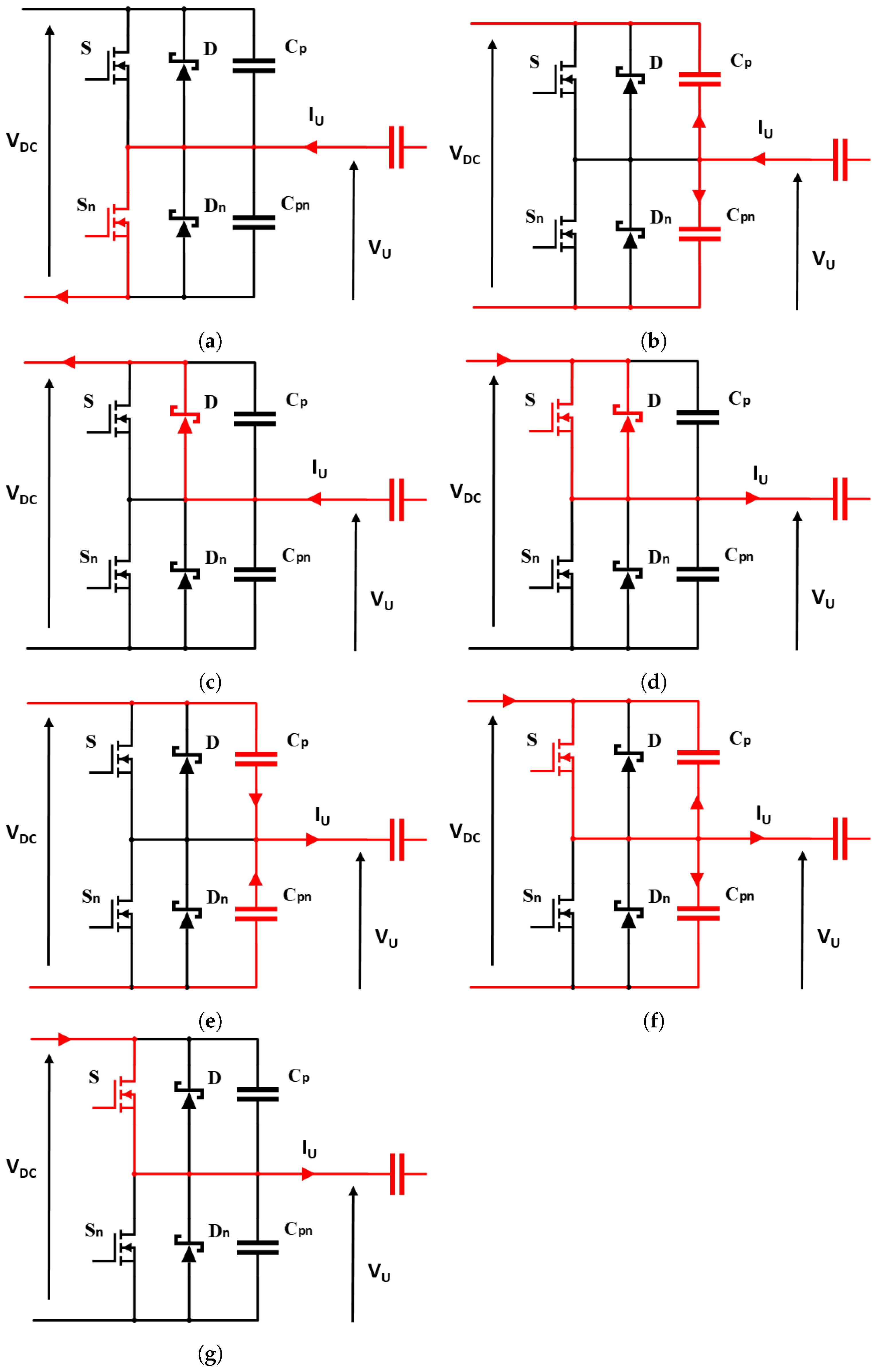
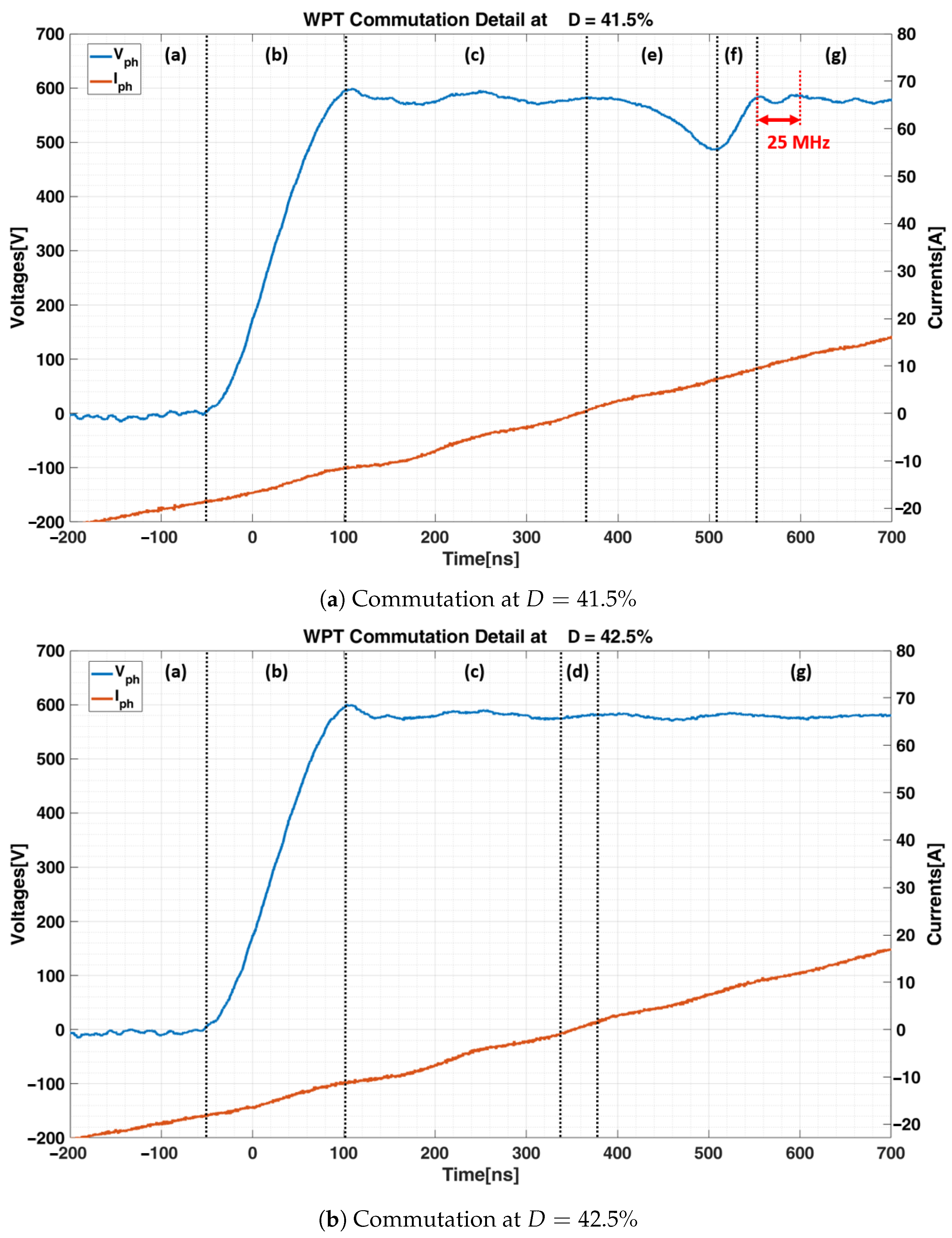
- a.
- Starting from a condition in which the low-side switch is in conduction state (Figure 13a) the phase voltage is zero and the phase current is negative.
- b.
- When is off the current flows through the parasitic capacitance and . The output voltage increase until the DC-link voltage is reached (Figure 13b).
- c.
- is equal to the DC-link voltage, the current forces the Schottky diode to pass in conduction mode. Then the current path in this period is provided by the diode (Figure 13c).
- d.
- The soft switching occurs when the high-side switch (S) is closed (Figure 13d) while the diode is in conduction mode.
- e.
- A duty cycle less than allow the to freely oscillate (Figure 13e). Due to the direction of the current the phase voltage decrease following the charging and discharging process of the parasitic capacitance.
- f.
- The high-side switch is turned on during the charging and discharging process of the parasitic capacitance. This led to a hard switching condition. The voltage across (S) differs from zero and the current has a positive value (Figure 13f).
- g.
- The high-side switch is on the state, keeping the at the DC-link level and the positive direction of the phase current (Figure 13g).
6. Conclusions
Author Contributions
Funding
Institutional Review Board Statement
Informed Consent Statement
Data Availability Statement
Acknowledgments
Conflicts of Interest
References
- Madawala, U.K.; Neath, M.; Thrimawithana, D.J. A Power–Frequency Controller for Bidirectional Inductive Power Transfer Systems. IEEE Trans. Ind. Electron. 2013, 60, 310–317. [Google Scholar] [CrossRef]
- Miller, J.M.; Onar, O.C.; Chinthavali, M. Primary-Side Power Flow Control of Wireless Power Transfer for Electric Vehicle Charging. IEEE J. Emerg. Sel. Top. Power Electron. 2015, 3, 147–162. [Google Scholar] [CrossRef]
- Li, W.; Zhao, H.; Li, S.; Deng, J.; Kan, T.; Mi, C.C. Integrated LCC Compensation Topology for Wireless Charger in Electric and Plug-in Electric Vehicles. IEEE Trans. Ind. Electron. 2015, 62, 4215–4225. [Google Scholar] [CrossRef]
- Covic, G.A.; Boys, J.T. Modern Trends in Inductive Power Transfer for Transportation Applications. IEEE J. Emerg. Sel. Top. Power Electron. 2013, 1, 28–41. [Google Scholar] [CrossRef]
- Covic, G.A.; Boys, J.T. Inductive Power Transfer. Proc. IEEE 2013, 101, 1276–1289. [Google Scholar] [CrossRef]
- Iruretagoyena, U.; Garcia-Bediaga, A.; Mir, L.; Camblong, H.; Villar, I. Bifurcation Limits and Non-Idealities Effects in a Three-Phase Dynamic IPT System. IEEE Trans. Power Electron. 2020, 35, 208–219. [Google Scholar] [CrossRef]
- Kim, S.; Covic, G.A.; Boys, J.T. Comparison of Tripolar and Circular Pads for IPT Charging Systems. IEEE Trans. Power Electron. 2018, 33, 6093–6103. [Google Scholar] [CrossRef]
- Cirimele, V.; Colussi, J.; Villa, J.L.; Ganga, A.L.; Guglielmi, P. Modelling of a 100 kW-85 kHz Three-Phase System for Static Wireless Charging and Comparison with a Classical Single-Phase System. In Proceedings of the IEEE International Symposium on Circuits and Systems (ISCAS), Seville, Spain, 10–21 October 2020; pp. 1–5. [Google Scholar] [CrossRef]
- Covic, G.A.; Boys, J.T.; Kissin, M.L.G.; Lu, H.G. A Three-Phase Inductive Power Transfer System for Roadway-Powered Vehicles. IEEE Trans. Ind. Electron. 2007, 54, 3370–3378. [Google Scholar] [CrossRef]
- Kim, M.; Kim, H.; Kim, D.; Jeong, Y.; Park, H.; Ahn, S. A Three-Phase Wireless-Power-Transfer System for Online Electric Vehicles With Reduction of Leakage Magnetic Fields. IEEE Trans. Microw. Theory Tech. 2015, 63, 3806–3813. [Google Scholar] [CrossRef]
- Thrimawithana, D.J.; Madawala, U.K. A three-phase bi-directional IPT system for contactless charging of electric vehicles. In Proceedings of the IEEE International Symposium on Industrial Electronics, Gdansk, Poland, 27–30 June 2011; pp. 1957–1962. [Google Scholar] [CrossRef]
- Iruretagoyena, U.; Villar, I.; Garcia-Bediaga, A.; Mir, L.; Camblong, H. Design and Characterization of a Meander-Type Dynamic Inductively Coupled Power Transfer Coil. IEEE Trans. Ind. Appl. 2017, 53, 3950–3959. [Google Scholar] [CrossRef]
- Cui, S.; Wang, Z.; Han, S.; Zhu, C.; Chan, C.C. Analysis and Design of Multiphase Receiver With Reduction of Output Fluctuation for EV Dynamic Wireless Charging System. IEEE Trans. Power Electron. 2019, 34, 4112–4124. [Google Scholar] [CrossRef]
- Li, H.; Liu, Y.; Zhou, K.; He, Z.; Li, W.; Mai, R. Uniform Power IPT System with Three-Phase Transmitter and Bipolar Receiver for Dynamic Charging. IEEE Trans. Power Electron. 2019, 34, 2013–2017. [Google Scholar] [CrossRef]
- Matsumoto, H.; Neba, Y.; Ishizaka, K.; Itoh, R. Model for a Three-Phase Contactless Power Transfer System. IEEE Trans. Power Electron. 2011, 26, 2676–2687. [Google Scholar] [CrossRef]
- Matsumoto, H.; Shibako, Y.; Shiihara, Y.; Nagata, R.; Neba, Y. Three-Phase Lines to Single-Phase Coil Planar Contactless Power Transformer. IEEE Trans. Ind. Electron. 2018, 65, 2904–2914. [Google Scholar] [CrossRef]
- Kim, S.; Covic, G.A.; Boys, J.T. Tripolar Pad for Inductive Power Transfer Systems for EV Charging. IEEE Trans. Power Electron. 2017, 32, 5045–5057. [Google Scholar] [CrossRef]
- Thrimawithana, D.J.; Madawala, U.K.; Francis, A.; Neath, M. Magnetic modeling of a high-power three phase bi-directional IPT system. In Proceedings of the IECON 2011—37th Annual Conference of the IEEE Industrial Electronics Society, Melbourne, Australia, 7–10 November 2011; pp. 1414–1419. [Google Scholar] [CrossRef]
- Song, Y.; Madawala, U.K.; Duleepa, J.T.; Hu, A.P. Cross coupling effects of poly-phase bi-directional inductive power transfer systems used for EV charging. In Proceedings of the IEEE 2nd International Future Energy Electronics Conference (IFEEC), Taipei, Taiwan, 1–4 November 2015; pp. 1–7. [Google Scholar] [CrossRef]
- Song, C.; Kim, H.; Jung, D.H.; Yoon, K.; Cho, Y.; Kong, S.; Kwack, Y.; Kim, J. Three-phase magnetic field design for low EMI and EMF automated resonant wireless power transfer charger for UAV. In Proceedings of the IEEE Wireless Power Transfer Conference (WPTC), Boulder, CO, USA, 13–15 May 2015; pp. 1–4. [Google Scholar] [CrossRef]
- Wang, C.-S.; Covic, G.A.; Stielau, O.H. Power transfer capability and bifurcation phenomena of loosely coupled inductive power transfer systems. IEEE Trans. Ind. Electron. 2004, 51, 148–157. [Google Scholar] [CrossRef]
- Cirimele, V.; Rosu, S.G.; Guglielmi, P.; Freschi, F. Performance evaluation of wireless power transfer systems for electric vehicles using the opposition method. In Proceedings of the IEEE 1st International Forum on Research and Technologies for Society and Industry Leveraging a Better Tomorrow (RTSI), Turin, Italy, 16–18 September 2015; pp. 546–550. [Google Scholar] [CrossRef]
- Pons, E.; Colella, P.; Rizzoli, R. Overvoltages in DC Urban Light Railway Systems: Statistical Analysis and Possible Causes. In Proceedings of the IEEE International Conference on Environment and Electrical Engineering and 2018 IEEE Industrial and Commercial Power Systems Europe (EEEIC/I CPS Europe), Palermo, Italy, 12–15 June 2018; pp. 1–6. [Google Scholar] [CrossRef]
- Zhou, H.; Chen, J.; Deng, Q.; Chen, F.; Zhu, A.; Hu, W.; Gao, X. Input-Series Output-Equivalent-Parallel Multi-Inverter System for High-Voltage and High-Power Wireless Power Transfer. IEEE Trans. Power Electron. 2021, 36, 228–238. [Google Scholar] [CrossRef]
- Zhang, B.; Carlson, R.B.; Galigekere, V.P.; Onar, O.C.; Pries, J.L. Electromagnetic Shielding Design for 200 kW Stationary Wireless Charging of Light-Duty EV. In Proceedings of the IEEE Energy Conversion Congress and Exposition (ECCE), Detroit, MI, USA, 11–15 October 2020; pp. 5185–5192. [Google Scholar] [CrossRef]
- Forest, F.; Huselstein, J.; Faucher, S.; Elghazouani, M.; Ladoux, P.; Meynard, T.A.; Richardeau, F.; Turpin, C. Use of opposition method in the test of high-power electronic converters. IEEE Trans. Ind. Electron. 2006, 53, 530–541. [Google Scholar] [CrossRef]
- Pries, J.; Galigekere, V.P.N.; Onar, O.C.; Su, G. A 50-kW Three-Phase Wireless Power Transfer System Using Bipolar Windings and Series Resonant Networks for Rotating Magnetic Fields. IEEE Trans. Power Electron. 2020, 35, 4500–4517. [Google Scholar] [CrossRef]
- Kim, S.; Covic, G.A.; Boys, J.T. Analysis on Tripolar Pad for Inductive Power Transfer systems. In Proceedings of the IEEE PELS Workshop on Emerging Technologies: Wireless Power Transfer (WoW), Knoxville, TN, USA, 4–6 October 2016; pp. 15–20. [Google Scholar] [CrossRef]
- Buja, G.; Bertoluzzo, M.; Mude, K.N. Design and Experimentation of WPT Charger for Electric City Car. IEEE Trans. Ind. Electron. 2015, 62, 7436–7447. [Google Scholar] [CrossRef]
- Ruffo, R.; Khalilian, M.; Cirimele, V.; Guglielmi, P.; Cesano, M. Theoretical and experimental comparison of two interoperable dynamic wireless power transfer systems for electric vehicles. In Proceedings of the IEEE Southern Power Electronics Conference (SPEC), Puerto Varas, Chile, 4–10 December 2017; pp. 1–6. [Google Scholar] [CrossRef]
- Zhang, W.; Mi, C.C. Compensation Topologies of High-Power Wireless Power Transfer Systems. IEEE Trans. Veh. Technol. 2016, 65, 4768–4778. [Google Scholar] [CrossRef]
- Sallan, J.; Villa, J.L.; Llombart, A.; Sanz, J.F. Optimal Design of ICPT Systems Applied to Electric Vehicle Battery Charge. IEEE Trans. Ind. Electron. 2009, 56, 2140–2149. [Google Scholar] [CrossRef]
- Zhang, Y.; Yan, Z.; Kan, T.; Zeng, X.; Chen, S.; Mi, C.C. Modeling and Analysis of a Strongly Coupled Series–Parallel-Compensated Wireless Power Transfer System. IEEE J. Emerg. Sel. Top. Power Electron. 2019, 7, 1364–1370. [Google Scholar] [CrossRef]
- Choi, J.; Tsukiyama, D.; Tsuruda, Y.; Davila, J.M.R. High-Frequency, High-Power Resonant Inverter With eGaN FET for Wireless Power Transfer. IEEE Trans. Power Electron. 2018, 33, 1890–1896. [Google Scholar] [CrossRef]
- Miller, J.M.; Daga, A. Elements of Wireless Power Transfer Essential to High Power Charging of Heavy Duty Vehicles. IEEE Trans. Transp. Electrif. 2015, 1, 26–39. [Google Scholar] [CrossRef]


| Three-Phase System Preliminary Values | ||
|---|---|---|
| Parameter | Variable | Value |
| Working frequency | 85 kHz | |
| DC input voltage | 580 V | |
| Litz wire cross section | 56 mm2 | |
| Coils external diameter | 710 mm | |
| Transmitter-Receiver airgap | 50 mm | |
| Transmitter self-inductance | 23.28 μH | |
| Receiver self-inductance | 23.28 μH | |
| Mutual inductance | 9.43 μH | |
| Resonant Capacitor | 170 nF | |
| Three-Phase System Measured and Testing Values | ||
|---|---|---|
| Parameter | Variable | Value |
| Resonance Frequency | 82.37 kHz | |
| Transmitter self-inductance | 23.46 μH | |
| Receiver self-inductance | 23.46 μH | |
| Error FEA vs manufactured inductance | 1% | |
| Mutual inductance | 8 μH | |
| Converter Reactive Components | ||
|---|---|---|
| Parameter | Variable | Value |
| DC-Link Bulk capacitors | 40 μF | |
| Fast SMD DC-Link capacitor | 4.7 nF | |
| Fast Film DC-Link capacitor | 1.8 μF | |
| Output Filter capacitor | 3 μF | |
| Parasitic Mosfet capacitance | 2.5 nF | |
| Mosfet Stray Inductance | 15 nH | |
| Measured Values of Electrical Quantities of the System | ||
|---|---|---|
| Parameter | Variable | Value |
| Supply voltage | 580.49 V | |
| Supply current | 14.83 A | |
| Supply Power | 8.61 kW | |
| WPT Input DC current | 192.12 A | |
| WPT Input Power | 111.52 kW | |
| WPT Output DC voltage | 378.87 V | |
| WPT Output DC current | 277.19 A | |
| WPT Output DC Power | 104.96 kW | |
| Boost Output DC current | 177.29 A | |
| Boost Output DC Power | 102.91 kW | |
| WPT efficiency | 94.12% | |
| Boost efficiency | 98.05% | |
Publisher’s Note: MDPI stays neutral with regard to jurisdictional claims in published maps and institutional affiliations. |
© 2021 by the authors. Licensee MDPI, Basel, Switzerland. This article is an open access article distributed under the terms and conditions of the Creative Commons Attribution (CC BY) license (https://creativecommons.org/licenses/by/4.0/).
Share and Cite
Colussi, J.; La Ganga, A.; Re, R.; Guglielmi, P.; Armando, E. 100 kW Three-Phase Wireless Charger for EV: Experimental Validation Adopting Opposition Method. Energies 2021, 14, 2113. https://doi.org/10.3390/en14082113
Colussi J, La Ganga A, Re R, Guglielmi P, Armando E. 100 kW Three-Phase Wireless Charger for EV: Experimental Validation Adopting Opposition Method. Energies. 2021; 14(8):2113. https://doi.org/10.3390/en14082113
Chicago/Turabian StyleColussi, Jacopo, Alessandro La Ganga, Roberto Re, Paolo Guglielmi, and Eric Armando. 2021. "100 kW Three-Phase Wireless Charger for EV: Experimental Validation Adopting Opposition Method" Energies 14, no. 8: 2113. https://doi.org/10.3390/en14082113
APA StyleColussi, J., La Ganga, A., Re, R., Guglielmi, P., & Armando, E. (2021). 100 kW Three-Phase Wireless Charger for EV: Experimental Validation Adopting Opposition Method. Energies, 14(8), 2113. https://doi.org/10.3390/en14082113