Article

Resonant Power Frequency Converter and Application in High-Voltage and Partial Discharge Test of a Voltage Transformer

by
Banyat Leelachariyakul
and
Peerawut Yutthagowith
*
King Mongkut’s Institute of Technology Ladkrabang, School of Engineering, 1 Chalongkrung Rd., Ladkrabang, Bangkok 10520, Thailand
*
Author to whom correspondence should be addressed.
Energies 2021, 14(7), 2014; https://doi.org/10.3390/en14072014
Submission received: 18 February 2021 / Revised: 19 March 2021 / Accepted: 22 March 2021 / Published: 5 April 2021
(This article belongs to the Special Issue Simulation and Analysis of High Voltage Engineering in Power Systems)

Abstract

:
This paper presents application of a resonant power frequency converter for high-voltage (HV) and partial discharge (PD) test of a voltage transformer. The rating voltage, power, and frequency of the system are 70 kVrms, 40 kVA, and 200 Hz, respectively. The testing system utilized the converter feeding to an HV testing transformer connected to a conventional partial discharge detection system. The converter system comprising a rectifier and insulated-gate bipolar (IGBT) switches with the H-bridge configuration was applied as a low-voltage source instead of a conventional motor-generator test set which requires large space and high cost. The requirements of the test according to the standards are quality of the test voltage and the background noise level. The required voltage must have the different voltage (DV) and total harmonic distortion (THDv) in the acceptable values of less than 5%. The DV is defined as the difference of the root mean square and peak voltages in percent. The required background noise level must be lower than 2.5 pC. Simulations and experiments were performed for verification of the developed system performance in comparison with those of the previously developed system based on the pulse width modulation converter. It is found that the developed system can provide the testing voltage with the DV and the THDv of lower than 1% and the background noise level of lower than 1 pC. Considering this achievement of promising performance, the developed system is an attractive choice for the HV and PD testing of voltage transformers in real practice.

1. Introduction

The main problem of the high-voltage (HV) and partial discharge (PD) test of voltage transformers is the applied voltage, which is higher than the transformer rating voltage. If such a voltage level with the rating frequency (50 Hz or 60 Hz) is applied to the test, it will lead to core saturation, high current consumption, and applied testing voltage distortion. For avoiding such conditions, the international standard defines the quality of the testing voltage with the different voltage (the root mean square value and peak value divided by square root of two) and total harmonic distortion, which are not higher than 5%. Under the test conditions, the applied voltage in such tests is not higher than two times the rating voltage of the transformer, so the applied voltage should have a frequency higher than two times that of the rating frequency. For safety reasons, the frequency used in the test is from 100 to 400 Hz. It is found that the frequency of 200 Hz is sufficient in all tests of the voltage transformers. Therefore, the 200 Hz frequency was utilized in all considered simulations and experiments. In the past, the motor and generator test set was applied in the test. However, the test set is quite costly, and it requires a large space for installation.
The high-voltage (HV) test is a crucial issue for the verification of the performance of the HV equipment in design and construction processes. Examples of such tests are insulation voltage withstand test, power loss measurement, dielectric loss measurement, and partial discharge measurement.
According to IEC 60270:2015, [1] partial discharges (PDs) are defined as localized electrical discharges that only partially bridge the insulation between conductors, and they are caused by local electrical stress concentrations in the insulation or on the surface of the insulation. Generally, such discharges appear as pulses with durations of less than 1 µs. PD measurement is the most important test used in the evaluation of insulation performance and life. The PDs are classified into three main types. The first type of the PD, named corona discharge, can occur in areas with sharp edges and high electric field stress. The second type originates from defects of the internal insulation material, such as bubbles and voids. If these defects have lower insulation levels than the main insulation material, under sufficient electrical field stress, PD can occur. The last PD type, called surface discharge, occurs at the boundary between two materials.
As the simplest way to generate HV for HV testing, [2] a voltage regulator connected with a power source from a low-voltage grid or a generator is applied to an HV testing transformer at the low-voltage side. The HV from the transformer is applied to a test object. Due to the nonlinear characteristic of the electrical and electronic equipment, the disturbance is generated in the electrical system, and it sometimes causes power quality problems, i.e., the voltage distortion and the background noise level. According to IEC 60060-1, [3] the testing voltage should be an almost purely sinusoidal waveform of which the total harmonic distortion voltage (THDv), defined by Equation (1), and different voltage (DV; peak voltage divided by √2 and RMS voltage) should be less than 5%.
T H D v = 1 V p 1 i = 2 50 V p i 2
Here, Vp1 is the peak voltage of the fundamental frequency and Vpi is the peak voltage of the ith harmonic frequency. Figure 1 shows the test voltage applied to the voltage transformer (VT) and PD pattern during the HV and PD test. It is found that the DV and THDv are higher than 5%. Additionally, the background noise level is higher than 2.5 pC (the acceptable background noise for the HV and PD test of the voltage transformers) [4,5]. To avoid the voltage distortion, and the unacceptable background noise level and to satisfy the standard requirements, an additional measure such as a voltage filter is necessary to be applied to the system.
For the HV test of voltage transformers (VTs) and to confirm the insulation performance of the test object, it is necessary to raise the voltage to be higher than the rating voltage. If the applied testing voltage with the rated frequency is used in the test, the core saturation of the voltage transformer can occur and the applied voltage may be distorted. For a better understanding, an example case should be considered. For the partial discharge test of a VT with the rating voltage (Ur) of 24 kV, the pre-stress voltage condition with a withstand voltage (Ut) of 80% is applied to the VT, and then the testing voltage is decreased to the level of 1.2Ur (28.8 kV) to record the PD activity. The procedure of applying voltage in the PD test is shown in Figure 2. Therefore, saturation of the iron core of VT is avoided by applying voltage with a frequency higher than the rated frequency of the VT. If the voltage with a power frequency of 50 Hz is applied to the HV side of the VT, the saturation effect of the VT will influence the distortion of the applied voltage waveform, as shown in Figure 1, and the DV and THDv will be higher than 5%. Aside from the nonlinear voltage, the core saturation can cause thermal runaway and explosion of PT. Therefore, to avoid the core saturation effect, a test voltage with a frequency higher than twice the power frequency is necessary in the test; the frequency of 200 Hz is a good candidate for all VTs with the rating frequencies of 50 and 60 Hz.
Nowadays, power electronics technology has been applied in many practical fields, such as home appliances, automotives and traction, renewable energy, and HV transmission and distribution systems. In HV generation for testing, the power electronics converter is a powerful and efficient tool for AC/DC, DC/AC, and AC/AC power conversion. However, the crucial problem of the application of the power converter in the PD test is the interference signal originating from fast switching of power electronic devices. It causes the PD detection system to have background noise much higher than the acceptable level. For example, in the PD tests of VTs insulated with oil, the acceptable PD level is only 5 pC [4,5]. Consequently, the testing system including the PD detection system should have a background noise level below 50% of the acceptable PD level (2.5 pC). Most commercial power converters have an additional filter for eliminating undesired harmonic voltage and obtaining a voltage waveform close to a pure sinusoidal wave. However, the filter cannot eliminate the interference in the PD measurement completely, leading the background noise in the PD test to be higher than the acceptable level.
Recently, there are attempts for development of the HV and PD test of voltage transformer. In [6,7,8,9], the power frequency converter based on the pulse width modulation (PWM) techniques was developed as the low-voltage source applied to the HV testing transformer for the HV and PD test. In [10,11], the analysis of effect of the additional filter for the reduction in the background noise in the HV and PD test was presented. In [12], the analysis of the PWM converter with the additional filter was presented, and the best switching frequency in terms of the quality of the generated voltage and background noise level were investigated. However, it is found that the developed system in [12] required the additional filter with quite large capacitance and high power consumption.
For overcoming such problems, the HV and PD testing system based on a resonant power frequency converter is proposed in this paper. Simulations were utilized for the design of the system, and experiments were performed to verify the validity of the developed system. The system performances in terms of the testing voltage quality and background noise level were investigated and analyzed in comparison with those of the previous developed system based on the pulse width modulation converter. It is found that the developed system performances are much superior to those of the previous system. The different voltage and total harmonic distortion of the testing voltage are less than 1%, and the background noise level is less than 1 pC at the rating voltage. From this achievement in terms of the system performances, the developed system is an attractive choice for the HV and PD testing of voltage transformers in the real practice.

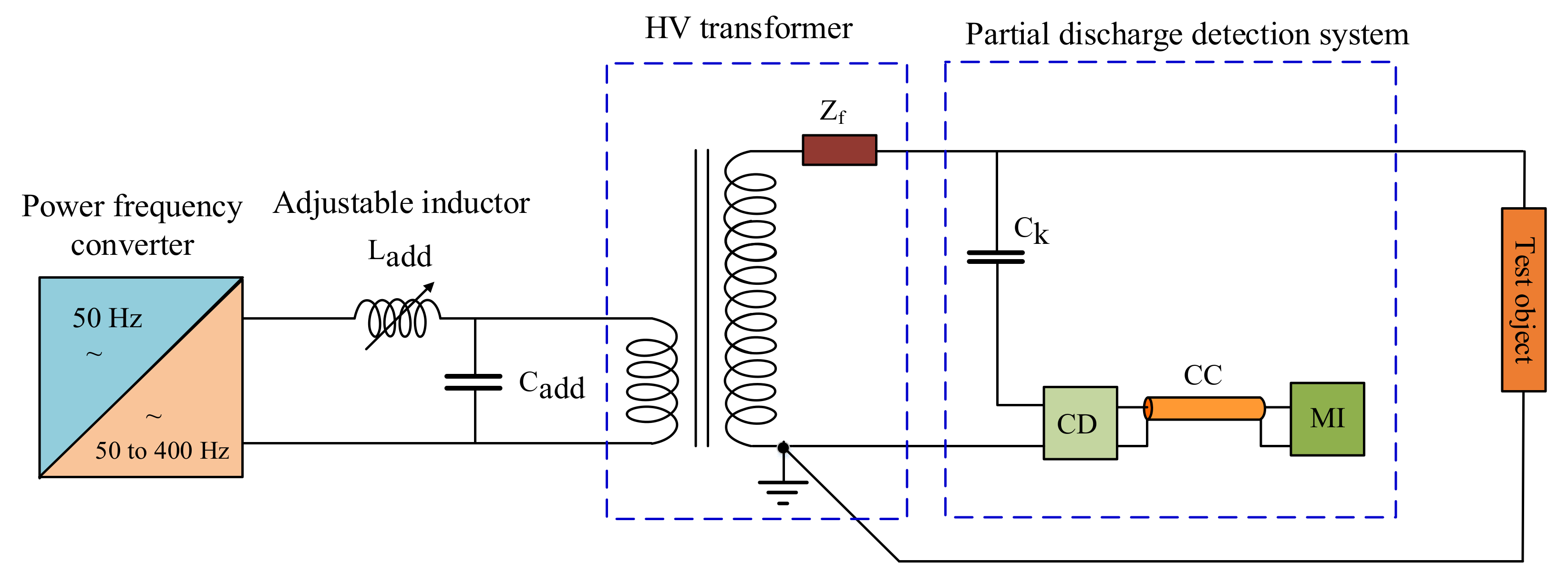
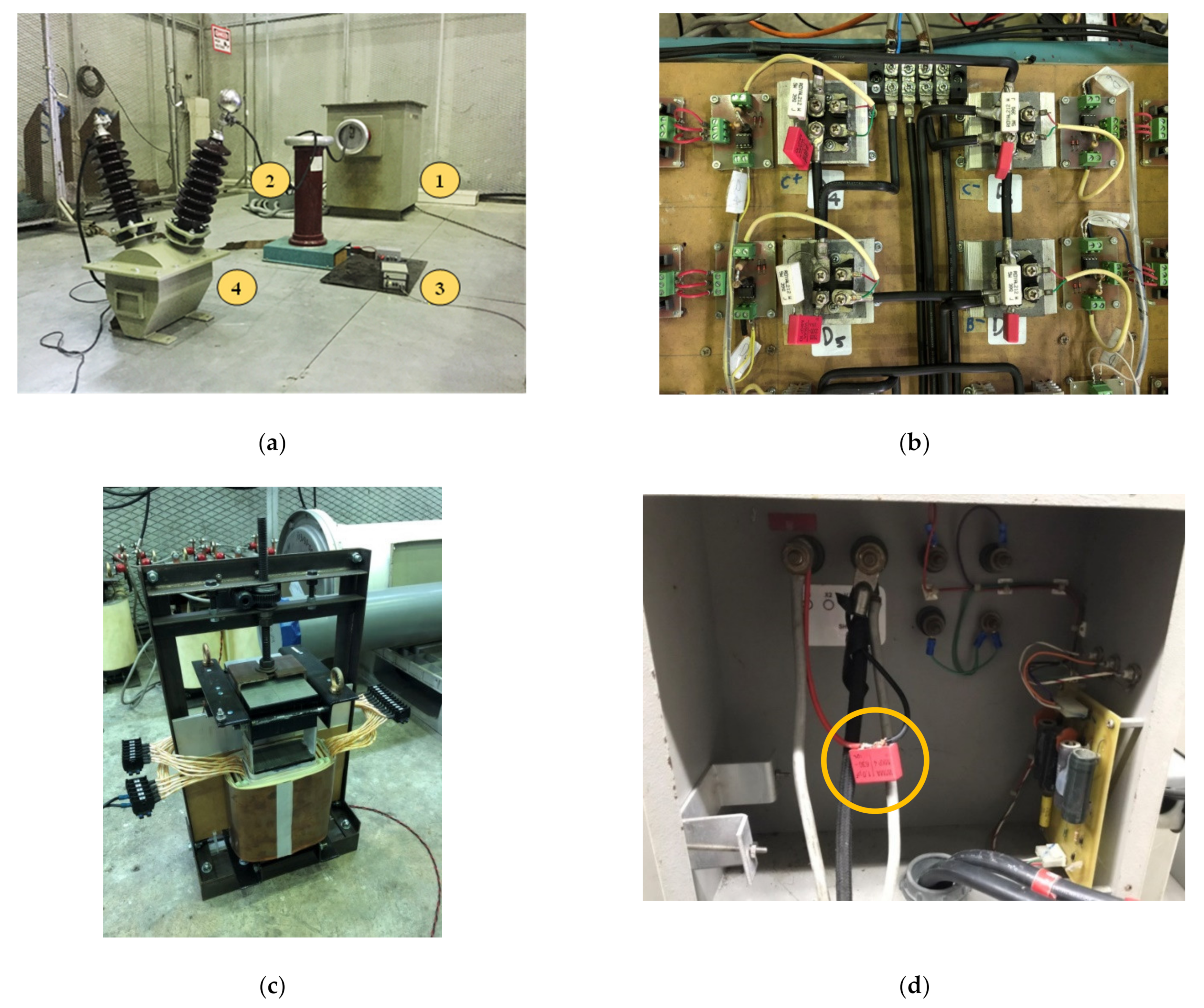
2. Development of HV Testing System for PD Tests

The developed system with the equivalent circuit shown in Figure 3 is composed of a power frequency converter, an additional inductor, an additional capacitor, an HV testing transformer, and a partial discharge detection system. Zf, Ck, CD, CC, and MI stand for the internal impedance of the testing transformer, the coupling capacitor, the coupling device or the measuring impedance, the measuring cable, and the measuring instrument, respectively.

2.1. Power Frequency Converter

The power frequency converter based on the H-bridge configuration, as shown in Figure 4, was developed. The converter is composed of a rectifier and H-bridge insulated-gate bipolar transistors (IGBTs), which can be controlled to generate either a square wave or pulse width modulation (PWM) waveforms.
The unipolar PWM technique [13,14,15] is based on operation of four control switches (S1, S2, S3, and S4) and four diodes (D1, D2, D3, and D4) as shown in Table 1. The AC output voltage waveform can instantaneously take one of the following three voltage levels: +Vdc, −Vdc, or 0.
The controlled and AC reference voltage waveforms are shown in Figure 5a, and the output signal is shown in Figure 5b.
For generation of the PWM waveform, the triangular waveform is set to be from 1.2 to 20 kHz. However, from the study in [12], it was found that the best performance of the PWM converter occurred at the switching frequency of 3.2 kHz. For generation of the square wave used in the proposed resonant circuit, the frequency of the triangular waveform is set to be the same as that of the control waveform.

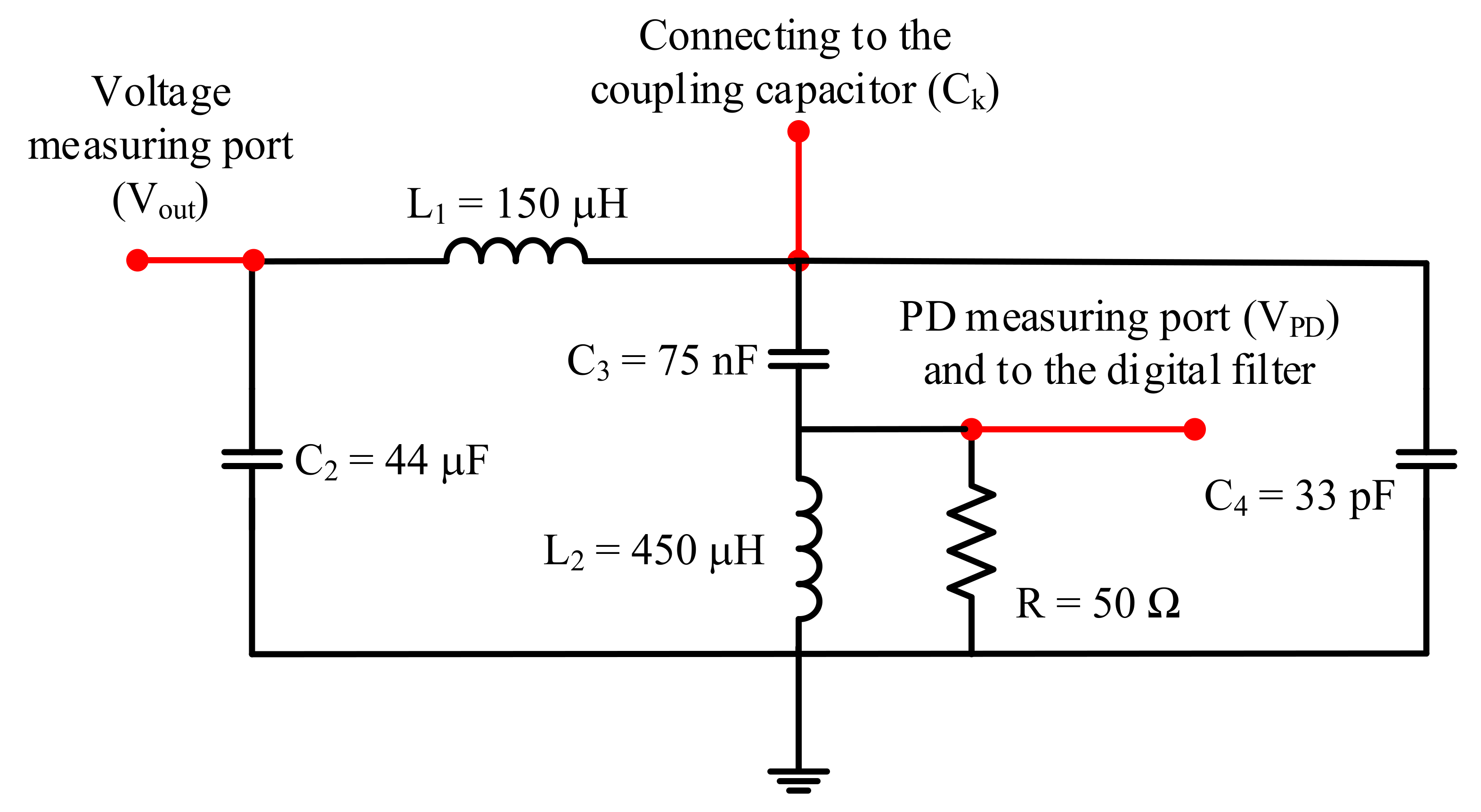
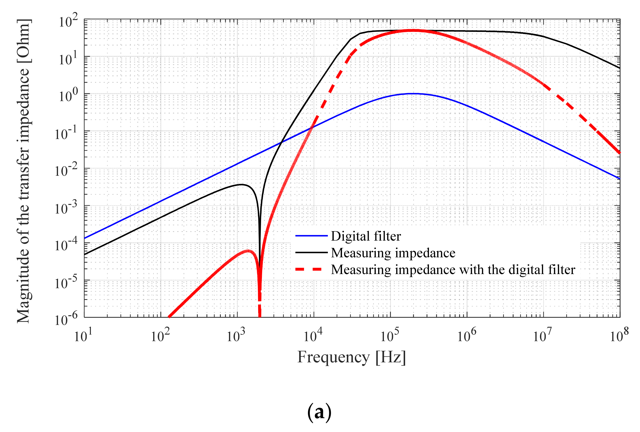
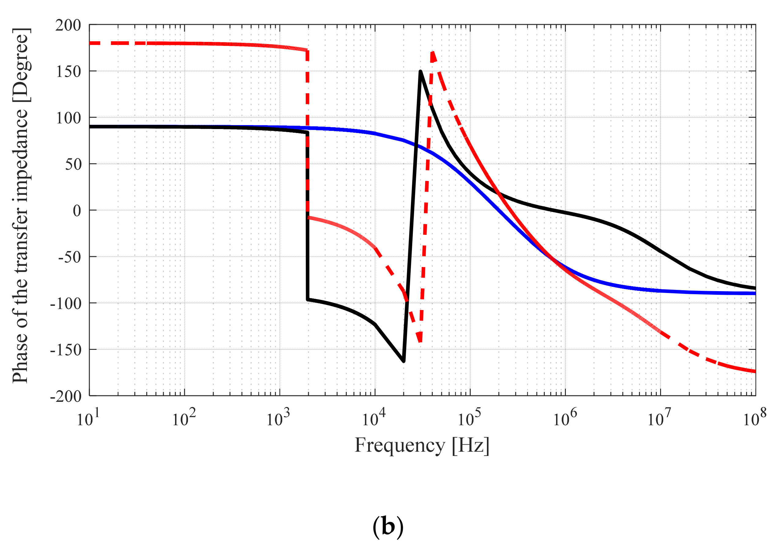
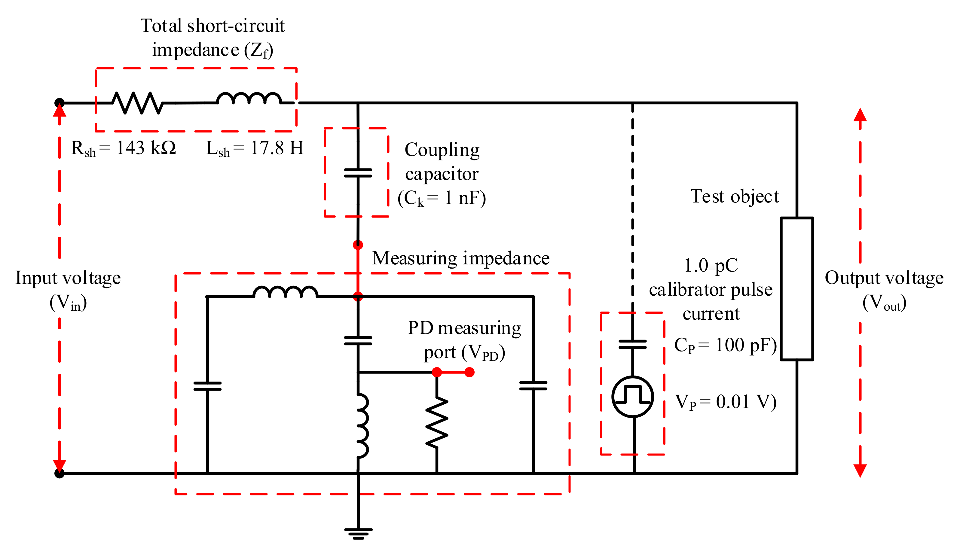
2.2. Partial Discharge Detection System

The developed partial discharge detection system is composed of a coupling capacitor (Ck) connected in series with the measuring impedance (coupling device). The capacitance Ck was selected to be 1 nF, and the measuring impedance was designed to have the band-pass characteristic with the equivalent circuit shown in Figure 6. The transfer impedance characteristic with the low and high cut-off frequencies of 30 kHz and 20 MHz, as shown in Figure 7. For avoiding the undesired noise signal in the HV testing environment, the standard [1] recommends using the band pass filter for a quasi-integration of the charge determination, and the acceptable range of cut-off frequencies of the filter are also provided [1]. In this paper, the digital band pass filter with the cut-off frequencies of 100 kHz and 400 kHz is utilized according to the standard requirement. The transfer function of the filter and the transfer impedance with the considered filter are also presented in Figure 7.
The equivalent circuit of the PD detection system with the HV testing transformer is shown in Figure 8. The crucial circuit parameters of the testing system are expressed in Table 2. The transfer function of the output voltage (Vout/Vin) can be calculated as shown in Figure 9 which shows that this transfer function has the characteristic of a low-pass filter. As shown in Figure 9, the cut-off frequency is about 1.2 kHz. It is noted that the total impedance of the HV testing transformer with the rating voltage of 460 V/75 kV and the rating power of 40 kVA is transferred to the HV side of the transformer. The circuit parameters are expressed in Figure 8, and the voltage transformer under test [16] or the test object can be represented well with a high impedance, which has an effect on the test circuit. When the 1 pC calibrator pulse current is injected into the system in the calibration process, the peak voltage response at the PD port and filtered peak voltage by the digital band pass filter are about 2.0 mV and 0.115 mV, respectively. The results of the response voltages are shown in Figure 10.
For a better understanding of the problem of using the PWM frequency converter in the HV and PD test, we should consider the case in which the 200 Hz PWM voltage of 100 kV with the switching frequency of 3.2 kHz is supplied to the system without an additional filter as shown in Figure 8. The voltage across the test object has small oscillation, as shown in Figure 11, and its THDv is 0.93%. The PWM voltage also affects the voltage at the PD measuring port. The peak voltages at the PD port and the filtered one are of 570 mV and 370 mV, respectively. As shown in Figure 12, the interference voltages are much higher than the peak voltage response of a 1 pC calibrator pulse. It can be seen that the band pass filter is not very effective for mitigation of the interference signal from the switching voltage. Therefore, the mean value for mitigating the interference from the PWM frequency converter is required for the PD test in real practice. In this paper, the additional inductor and capacitor are proposed to connect at the LV side of the HV testing transformer for obtaining the resonant condition. The analysis of the additional circuit components will be presented in the next Section 2.3.

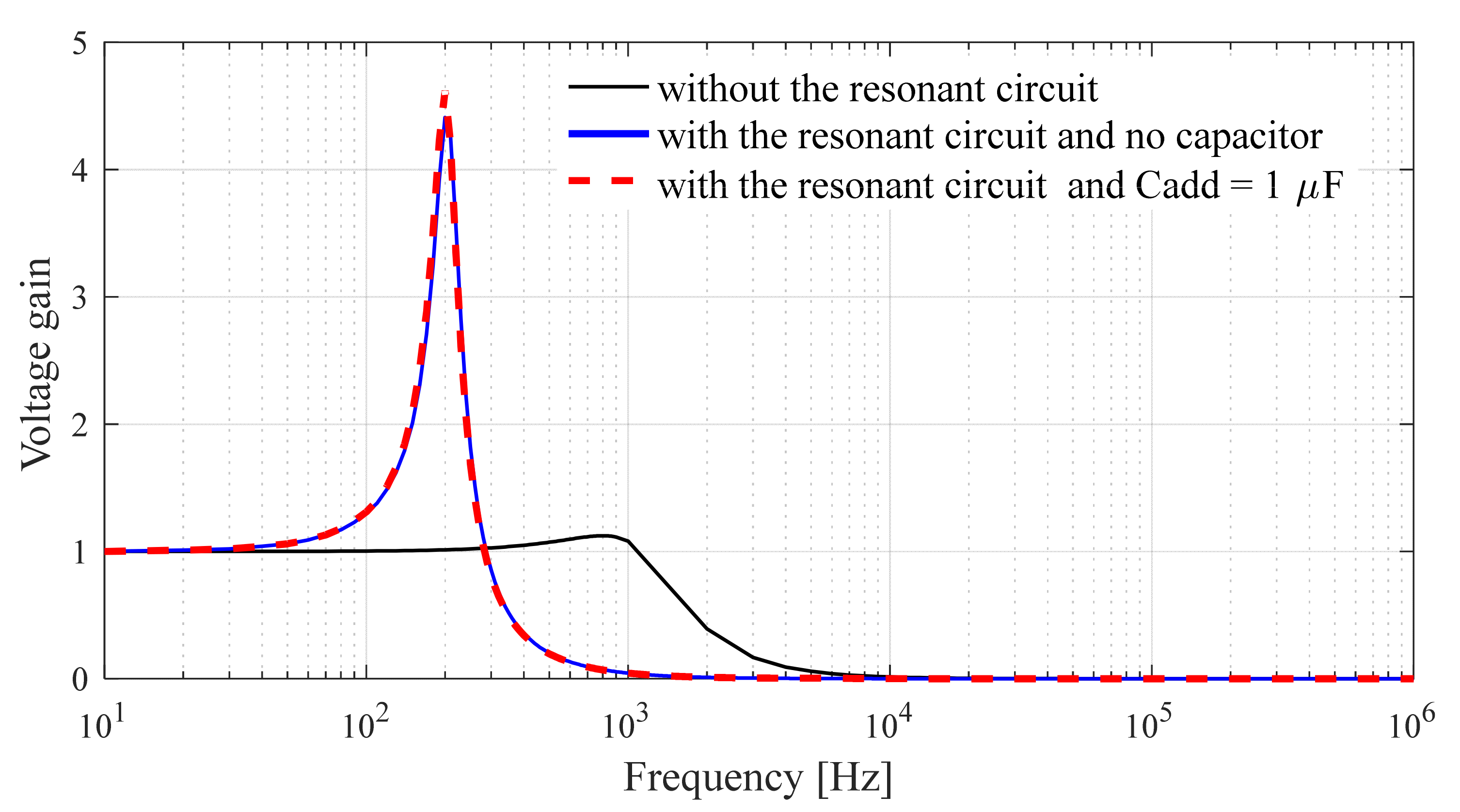
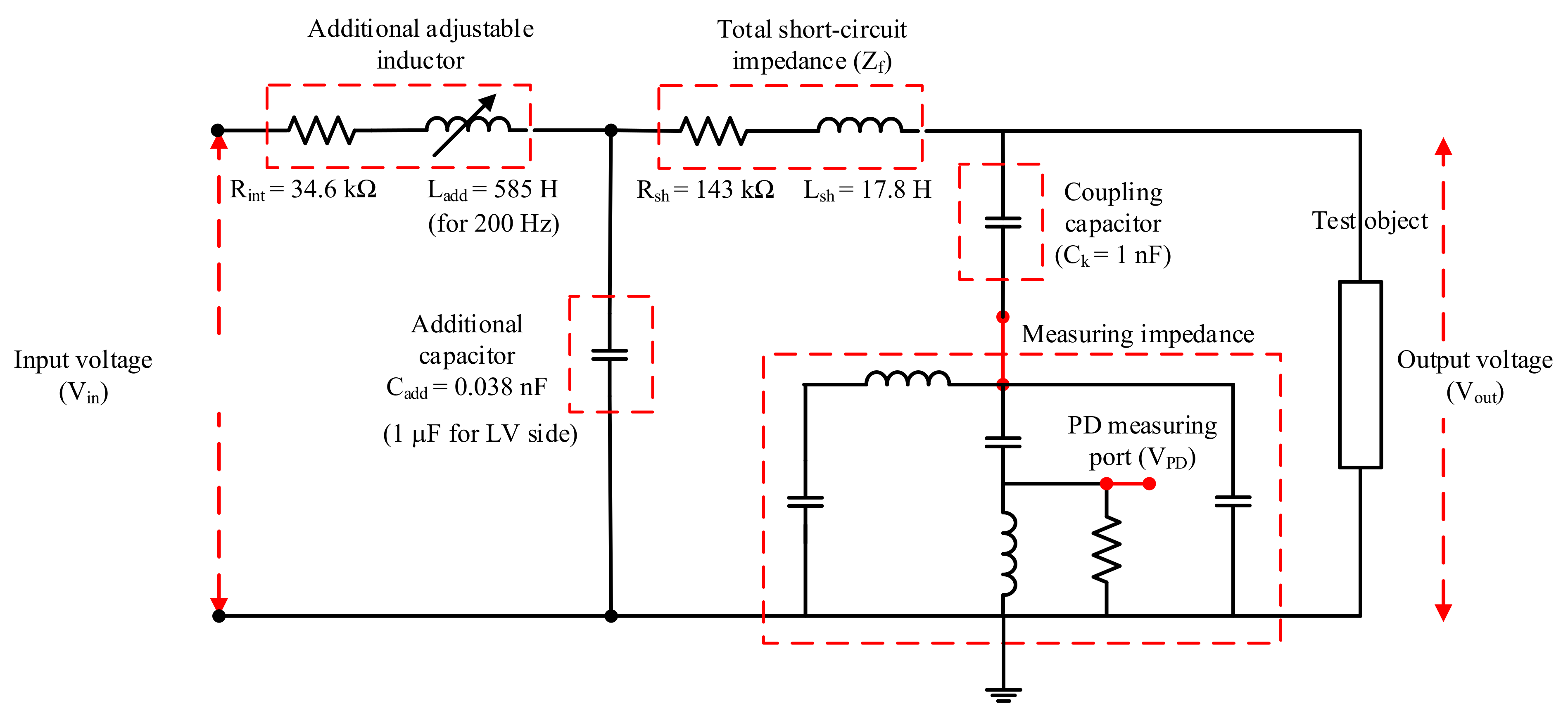
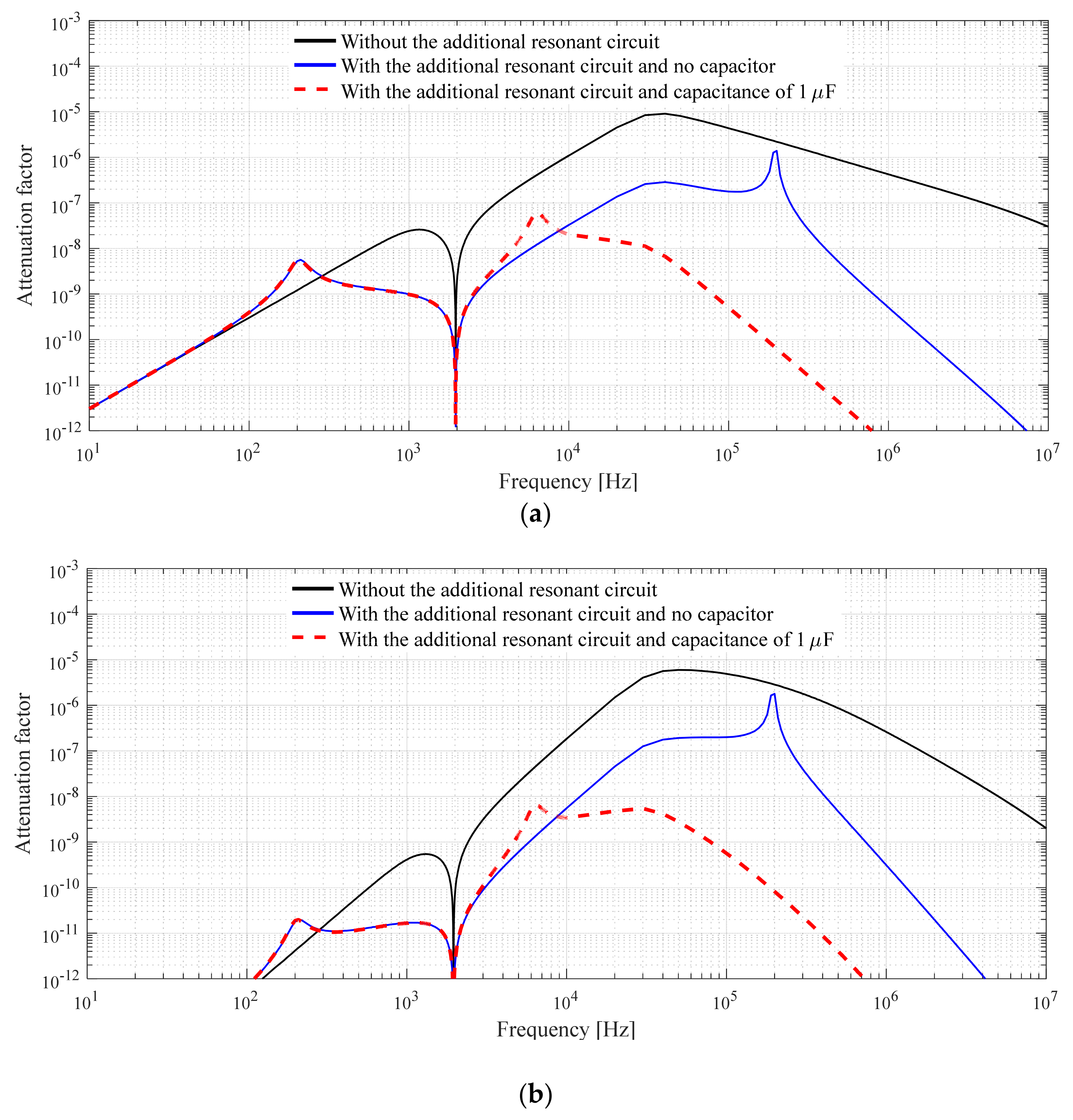
2.3. Additional Circuit for Circuit Resonance
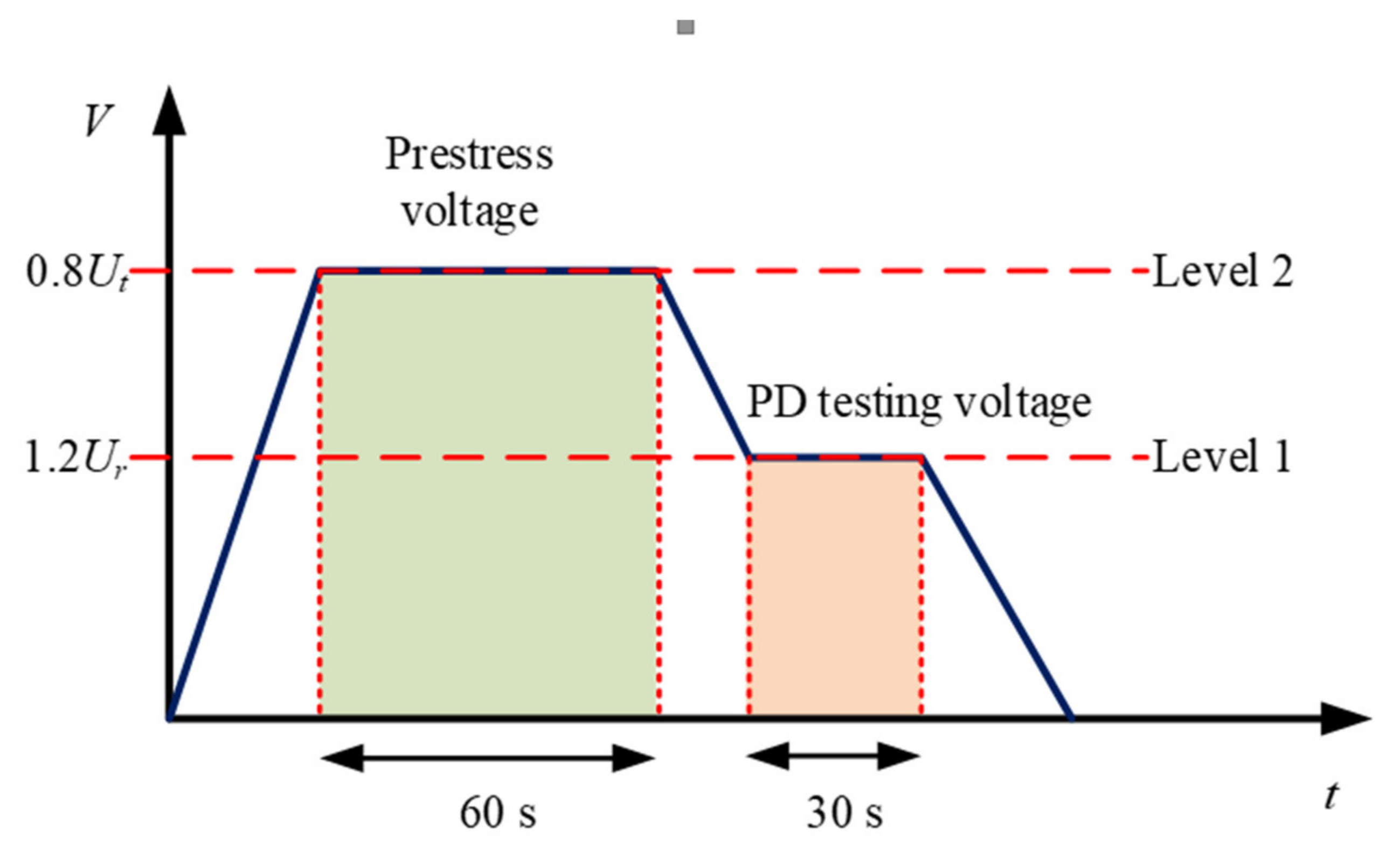
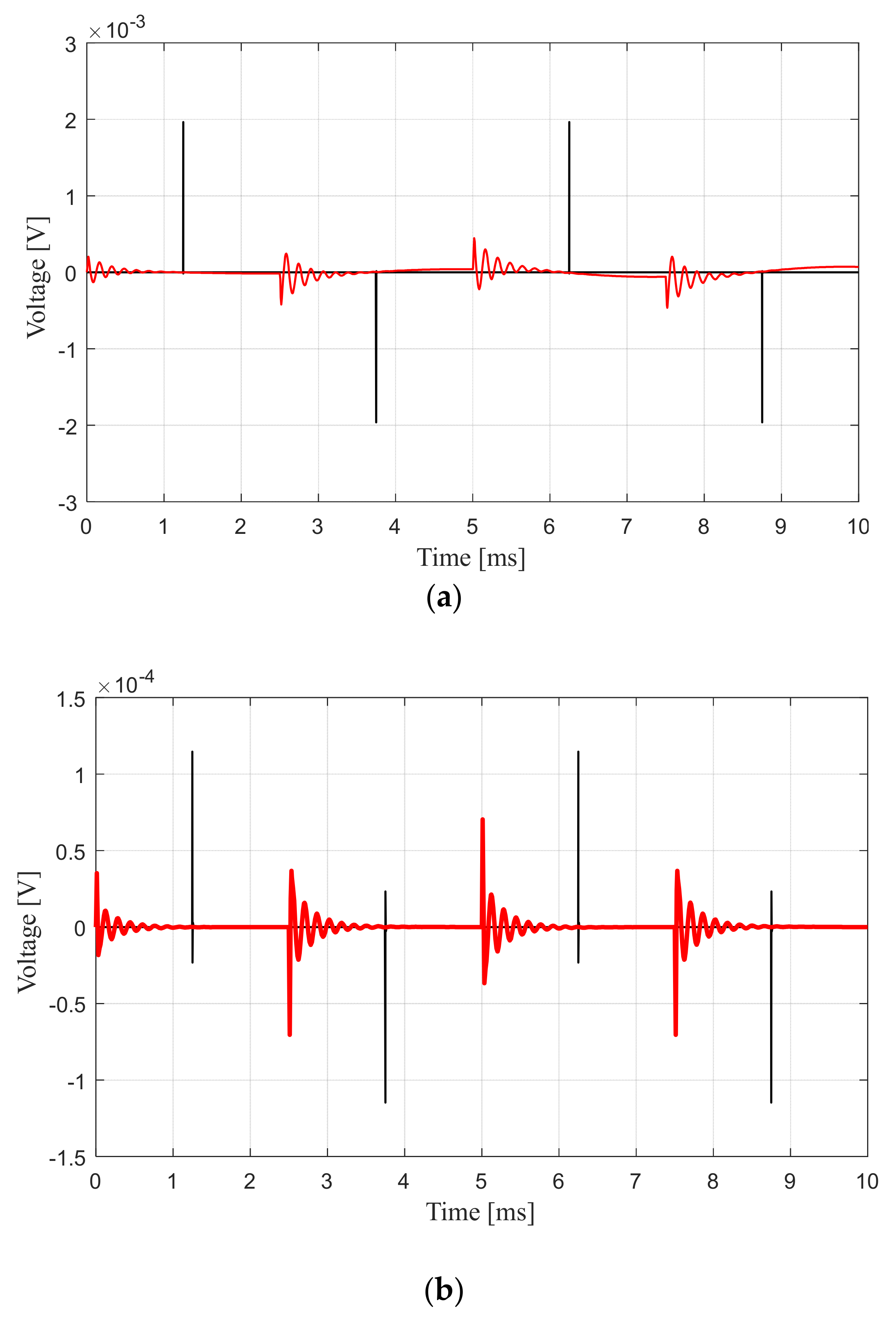
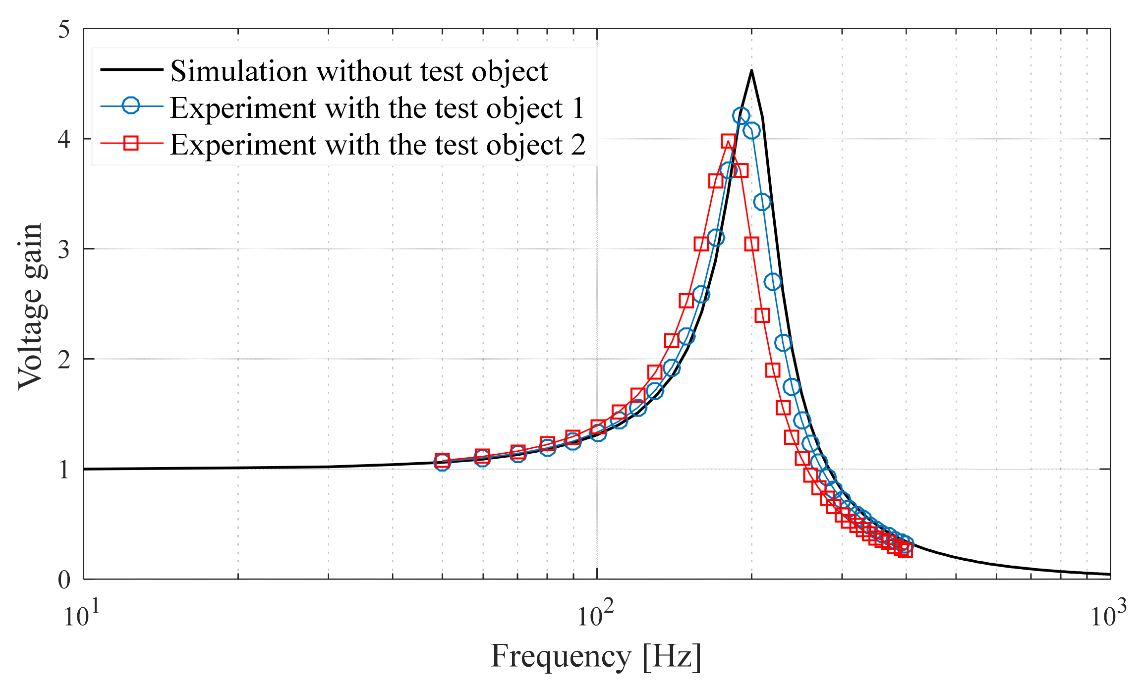
To reduce the noise level, the additional filter is required as in the previous studies [6,7,8,9,10,11,12]. In this paper, an additional adjustable inductor and capacitor are proposed to add in the low-voltage side of the testing transformer for obtaining the resonant condition of the test circuit as shown in Figure 3. The inductance was adjusted to obtain the resonant condition at the frequency of 200 Hz. With the circuit parameters of the testing system, the series resonant condition is occurred by Equation (2), where Lt is total inductance and Ct is total capacitance. In the considered system, the total capacitance can be approximated as the coupling capacitance (Ck). The required additional inductance (Ladd) can be calculated by Equations (2) and (3), and the result is about 23 mH.
L t = 1 ω 2 C t
L t = L a d d + L s h
The voltage gain at the resonant condition is equivalent to the quality factor (Q) as expressed in Equation (4), where Rt is total series resistance composed of internal resistance (Rint) of the additional inductor and series resistance of the testing transformer (Rsh).
Q = L t / C t R t
In this paper, the required Q was set to be not less than 4 which is sufficient for obtaining the almost pure sinusoidal output voltage. It is noted that the quality factor of 4 will be confirmed to be sufficient by the simulation result in the Section 3. For the designed inductor, the internal resistance is necessary to be controlled for obtaining the desired Q. The maximum internal resistance (Rint) can be calculated by Equation (5), and the result is 2.0 Ω.
R t = R int + R s h
From the calculation above, the adjustable inductor was designed by a manufacturer. The inductance of the developed adjustable inductor can be varied from 10 to 40 mH, and the internal resistance is 1.3 Ω.
The equivalent circuit of the HV and PD testing system is expressed in Figure 13. All circuit parameters in Figure 13 were transferred to the HV side of the testing transformer. It is noticed on the equivalent circuit in Figure 8 that the inductor will not affect the PD measurement if the PD occurs on the HV side. The transfer function in the form of the attenuation factor (VPD/Vin) can be determined as the results in Figure 14a and the attenuation factor with the band pass filter recommended by the standard are expressed in Figure 14b. The input square wave voltage generated by the converter of 17.1 kV (corresponding to 100 kV output voltage) and the output voltage are expressed in Figure 15. The black line stands for the input voltage of the HV testing transformer (transferred to the HV side of the testing transformer), and the red line stands for the output voltage of the testing transformer or the voltage across the test object. It is noticed that the output voltage waveform is almost pure sine due to the occurrence of resonant condition at the frequency of 200 Hz. It is also confirmed that the quality factor of 4 is sufficient to obtain the waveform as the standard requirement.
In the results shown in Figure 16 and Figure 17. The black line is denoted for the voltage response of 1 pC calibrator pulse current, and the red line stands for the interference signal at the output voltage of 100 kV. Without the additional capacitor (Cadd), the interference from the square wave as the input voltage of the testing transformer is still high. Additionally, the band pass filter recommended by the standard is not particularly effective for mitigation of the attenuation of the interference signal, as shown in Figure 16. With connection of the additional capacitor (Cadd), the interference is attenuated to be lower than the voltage response of the 1 pC calibrator pulse current. Additionally, the band pass filter recommended by the standard is quite effective for mitigation of attenuation of interference signal as it is shown in Figure 17. In Figure 17b, the maximum interference signal is 0.07 mV, which is equivalent to background noise level of 0.6 pC (0.115 mV is equivalent to the PD level of 1 pC).

3. Experiments

Some experiments were carried out to investigate the performance of the developed system in the partial discharge tests. The experimental setup is shown in Figure 18. The circuit parameters were set to be the same as in Figure 13. The performances of the developed system were investigated in terms of the different voltage, total harmonic distortion of the output voltage, and the background noise.
To avoid interference signal from electromagnetic coupling in the HV laboratory, the commercial EO/OE converters (Omicron) [17] with fiber optic cables were applied with the developed system. In the real PD test, the standard PD current with the charge of 5 pC was utilized in the calibration process. The background noise without the application of the developed inverter is about 0.8 pC. The experiments are separated into two topics as follows.

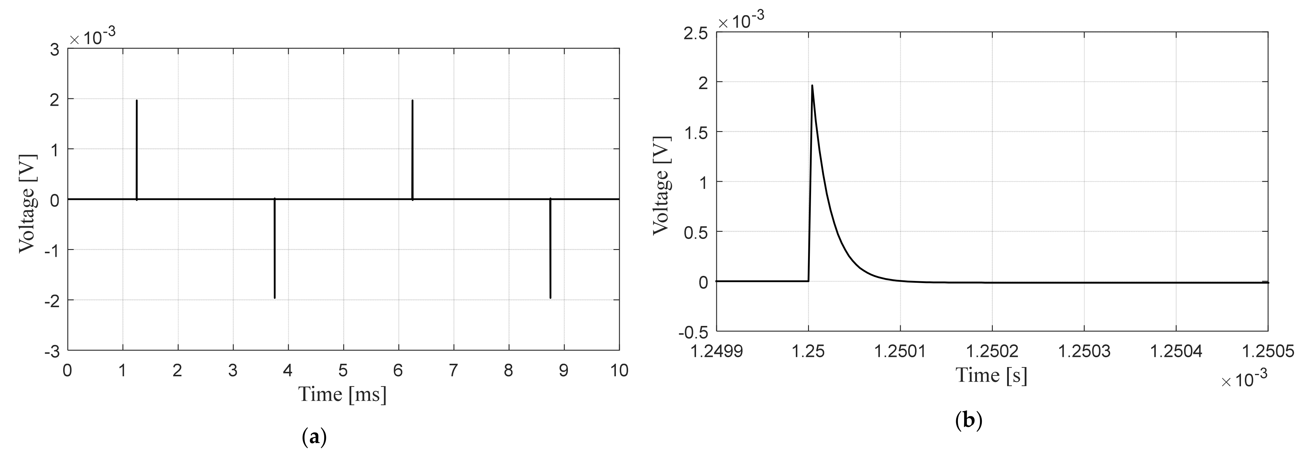
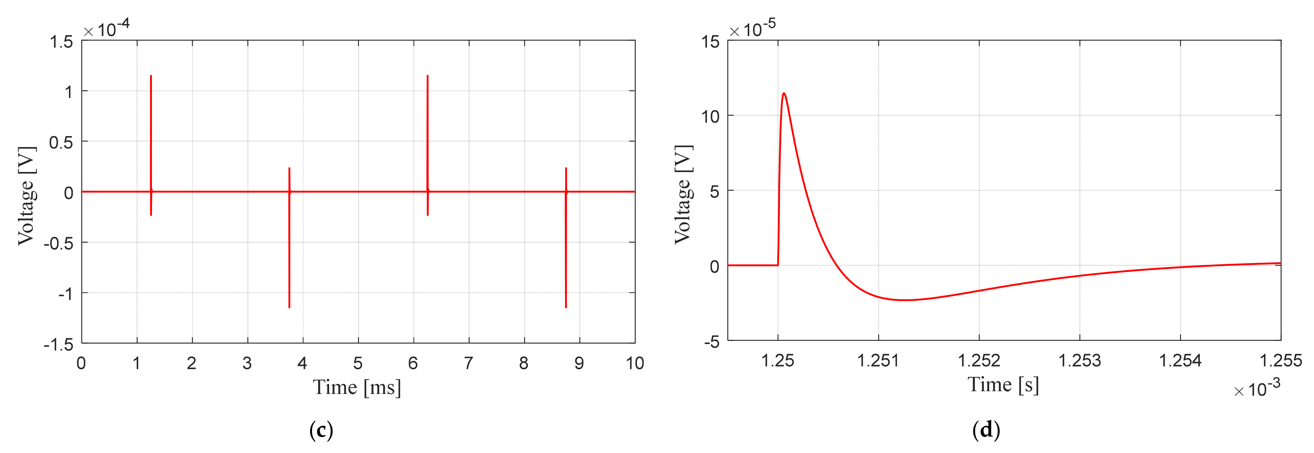
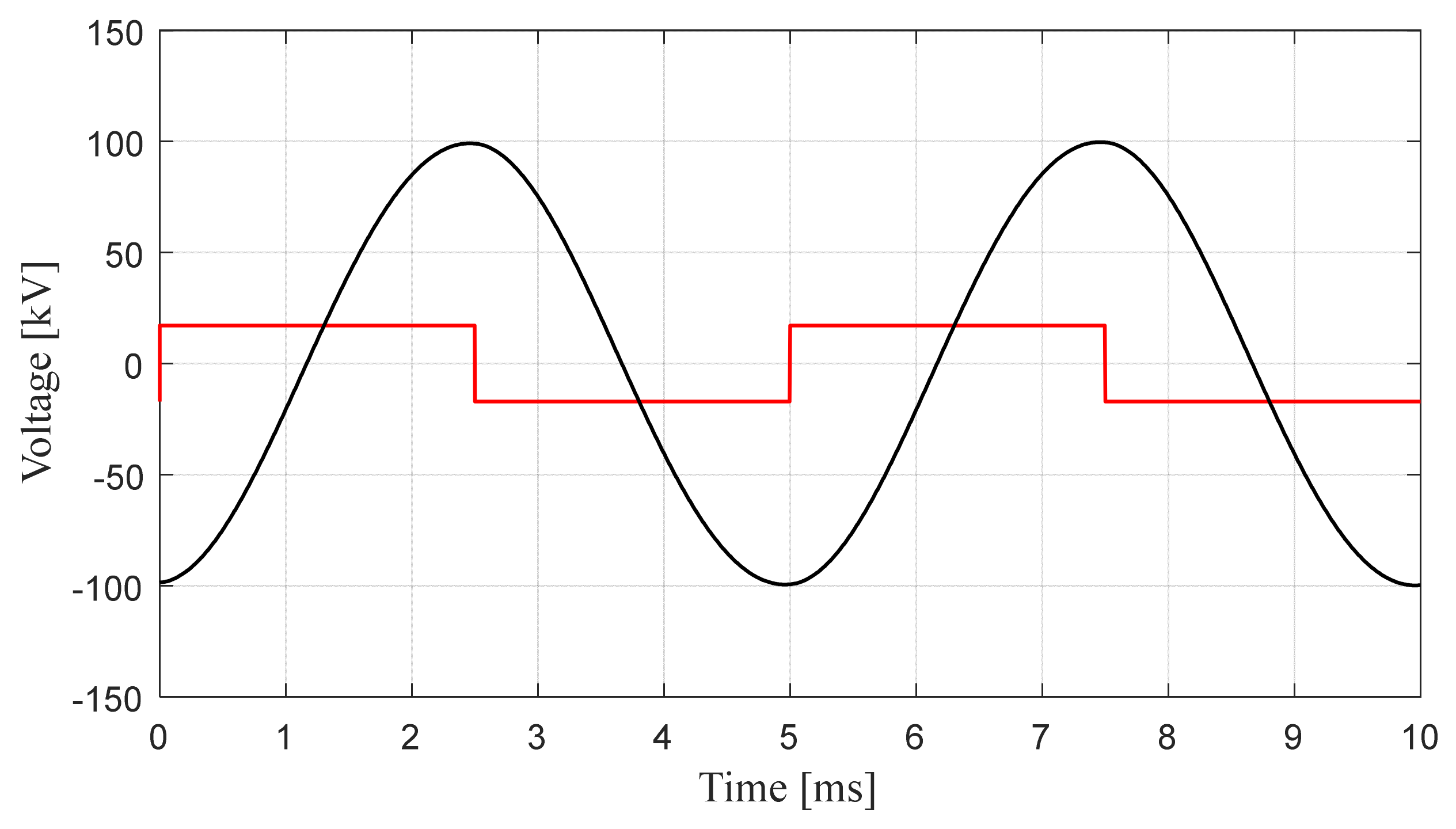
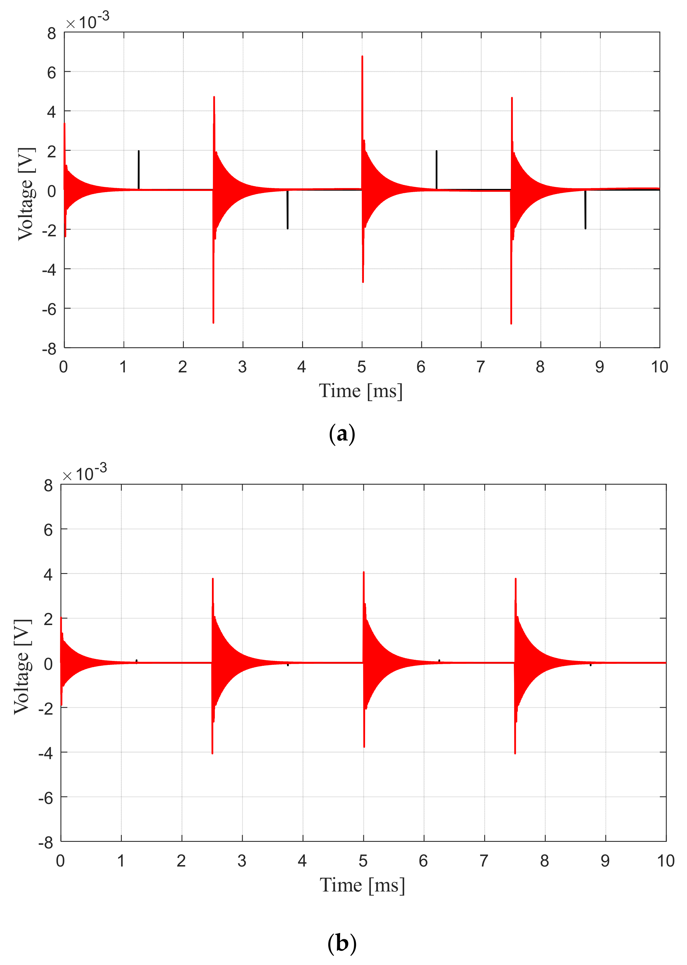
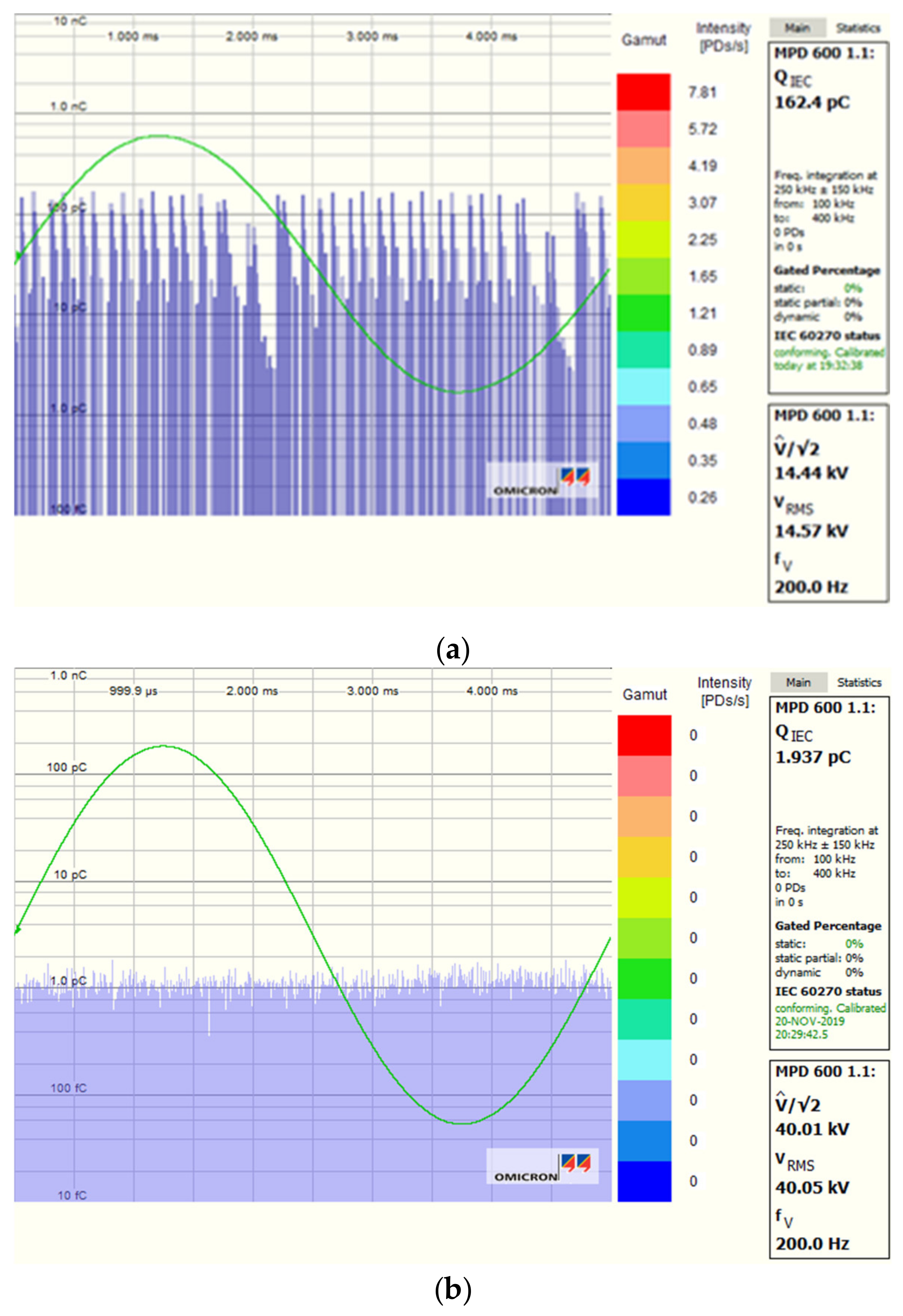
3.1. Experiments without Test Object

The experiments in this part are performed to examine the performance of the developed system in comparison with the previous developed system (the PWM converter with the switching frequency of 3.2 kHz) [12]. There is no test object connected to the test system. As shown in Figure 19a, the PWM system without an additional filter provides very high interference. However, when the additional filter was connected to the system, at the pre-stress voltage of 40 kVrms, the background noise was reduced significantly to be about 2.0 pC, as shown in Figure 19b. The DC input voltage supplied to the converter was about 370 V. The different voltage and THDv are 0.66% and 0.80%, respectively.
When the developed resonant system was considered, in the case of no connection of the additional capacitor, the acceptable background noise (2.5 pC) was reached at the output voltage of about 5 kV, as shown in Figure 20a. This agreed with the simulation result in Figure 16b. The interference signal of 4 mV is equivalent to the background noise level of 34.78 pC (4/0.115). With the same proportion of the simulation result, the background noise level should be 2.48 pC (34.78 × 5/70). In the case of connection of the additional capacitor, the background noise level at the output voltage is still the same as that of no application of the converter to the system, as shown in Figure 20b. At the output voltage of 40 kVrms, the DC input voltage supplied to the converter was about 83 V, which corresponds to the voltage gain of 4.5—this agreed with the simulation results. The different voltage and THDv are 0.61% and 0.35%, respectively.

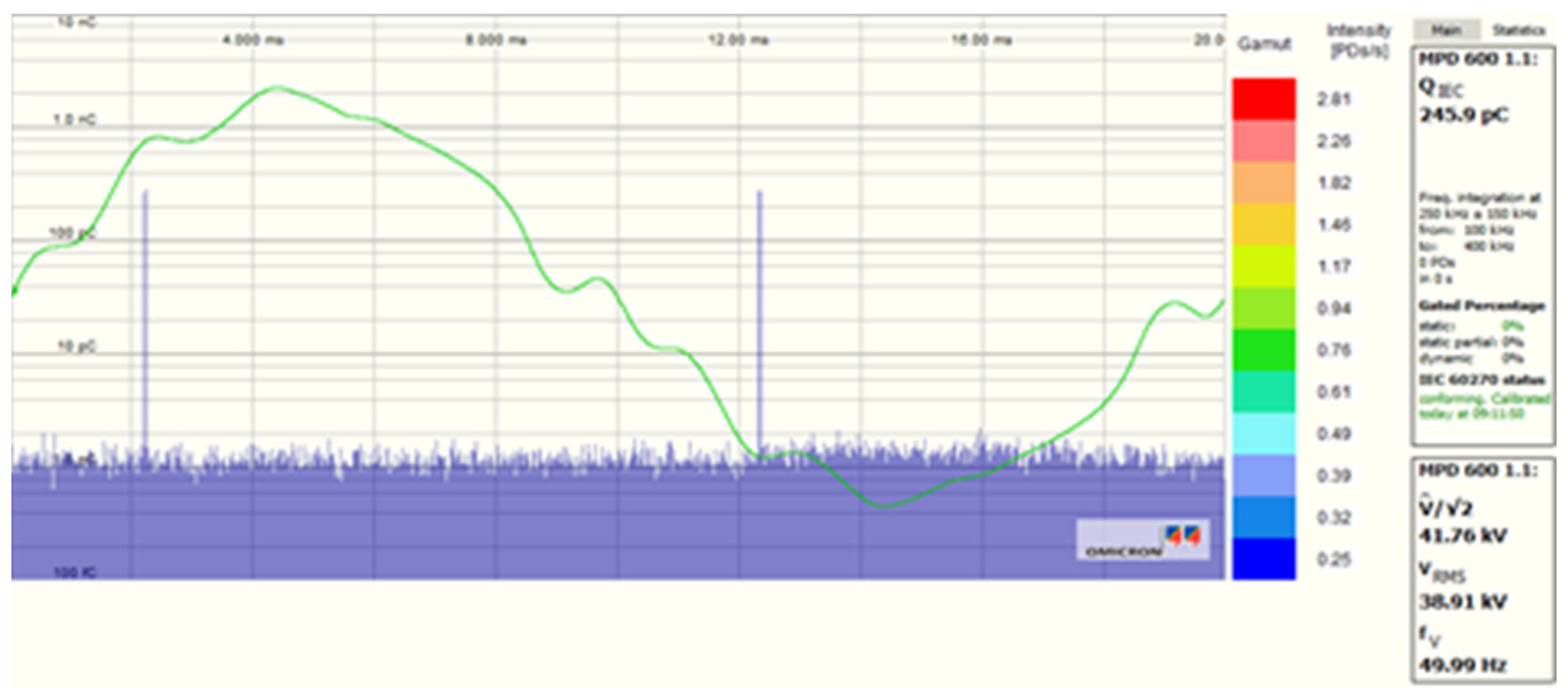
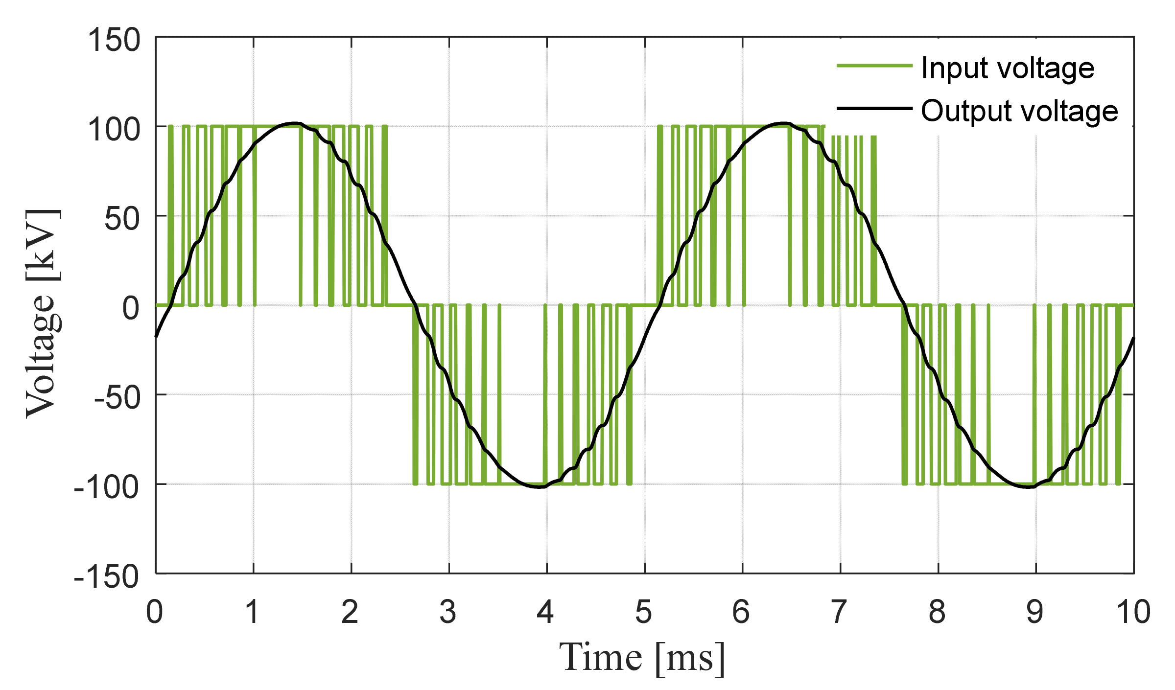
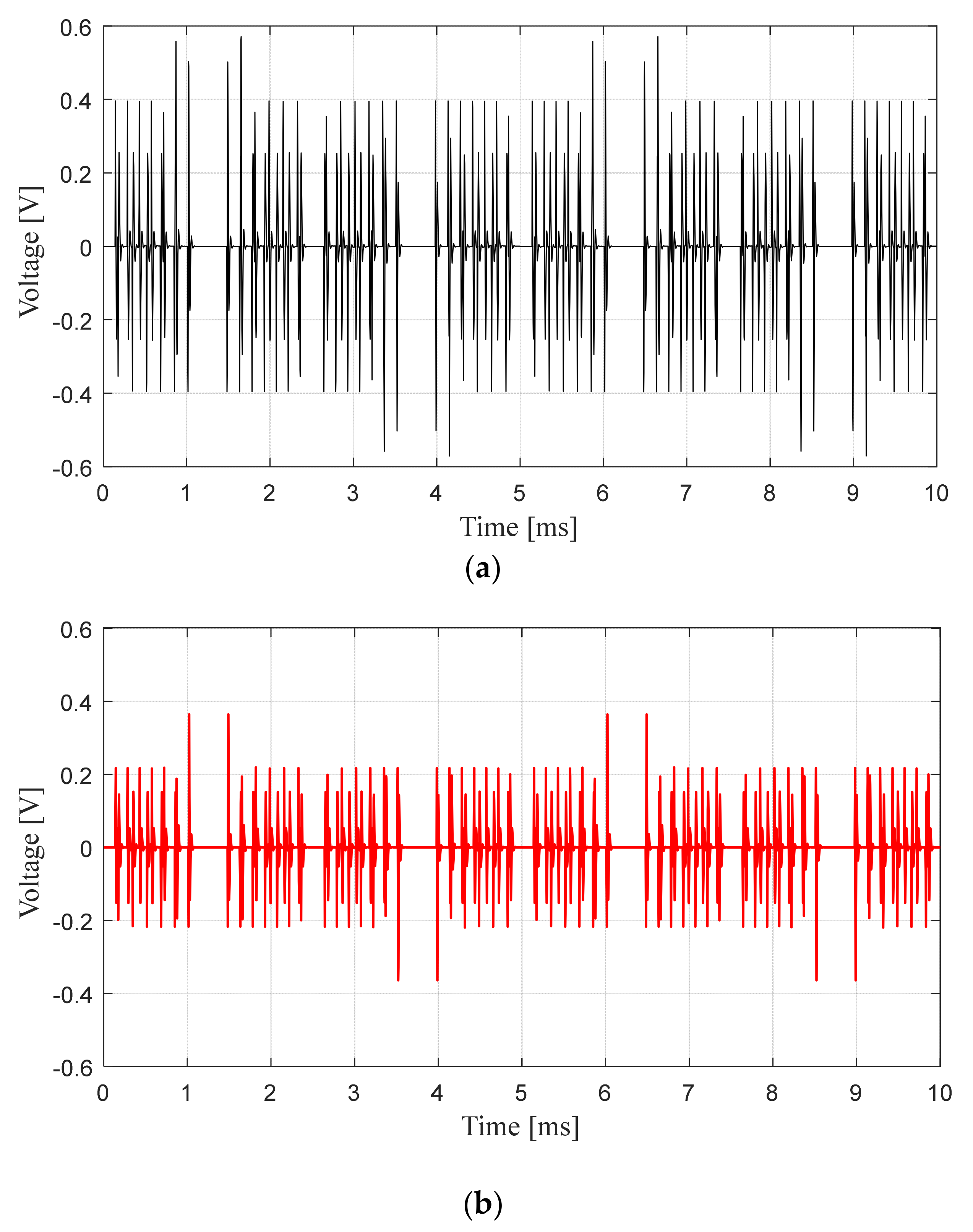
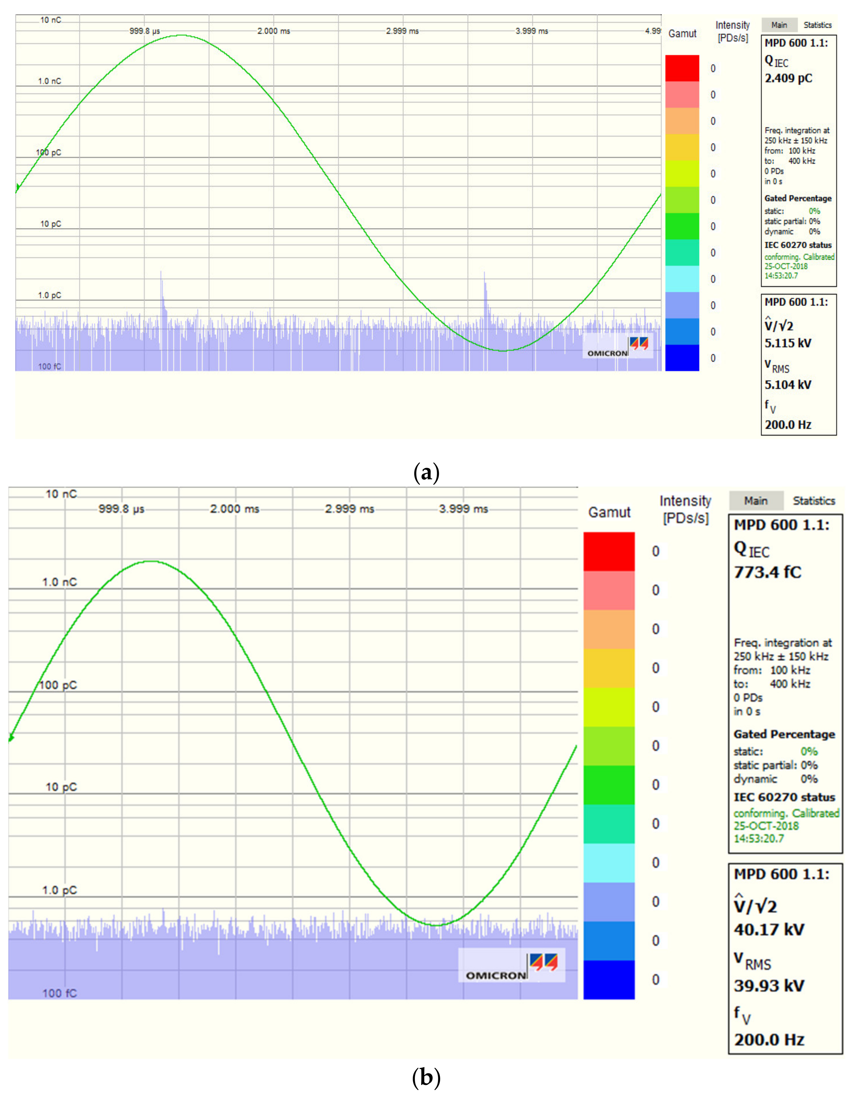
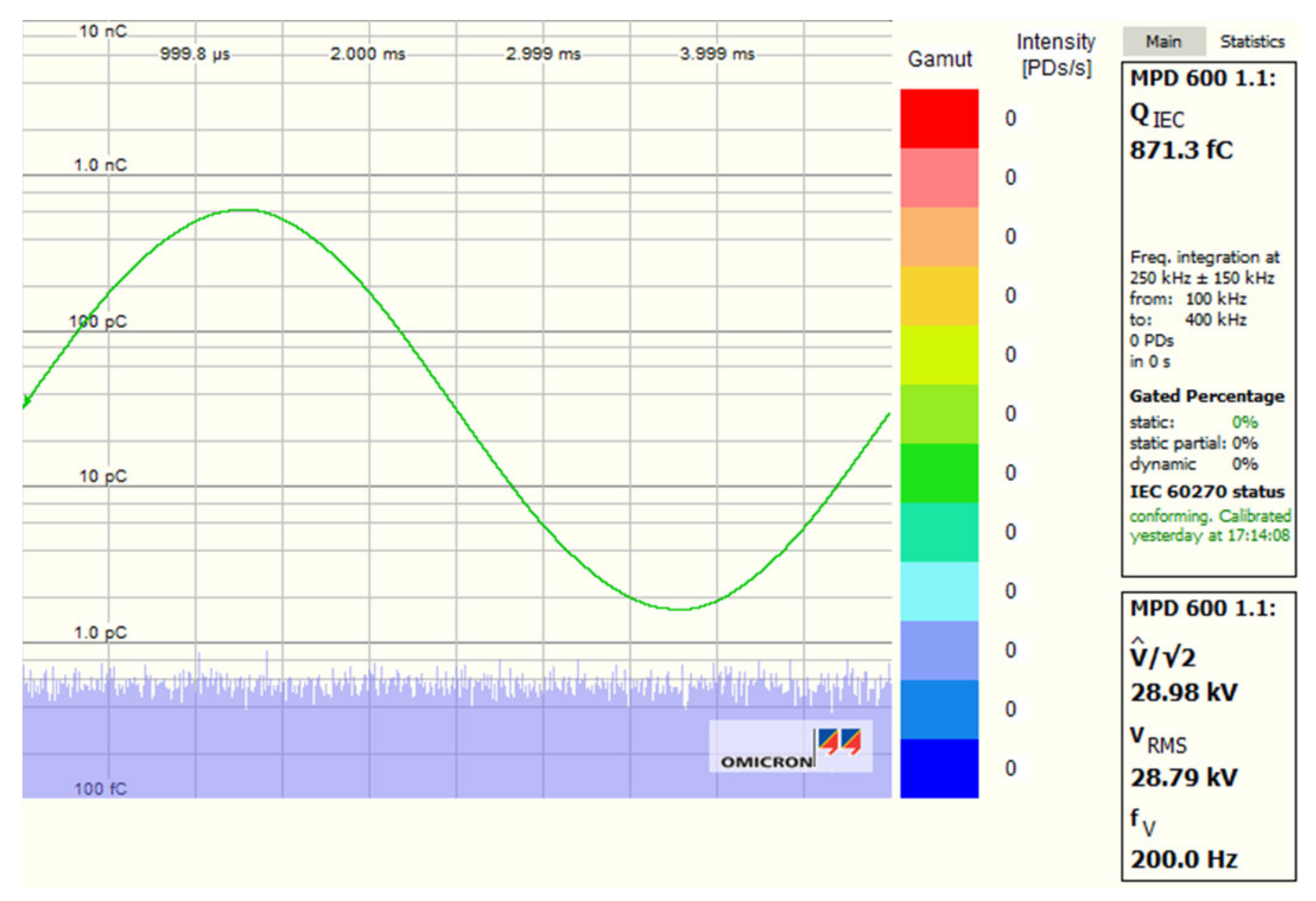
3.2. Experiment with a Test Object

For confirming validity of the developed system, two voltage transformers (test object 1 and 2) were tested. The frequency of the input voltage varied from 50 to 400 Hz for examining the voltage gain. The experimental results in comparison with the simulation result without test object are expressed in Figure 21. It is found that the test object does not affect much the voltage gain. The voltage gain at the resonant frequency is still higher than in all considered cases.
The other experiment was performed to confirm the performance of the developed system in the PD test with a VT. The voltage was raised up to 40 kVrms for the prestress condition and decreased to 30 kVrms for recording PD activity. The standard PD pulse with a charge of 5 pC is used for calibration in the PD test. The experimental results at the testing voltage of about 30 kVrms are shown in Figure 22. The different voltage (peak voltage/√2 = 28.98 kV and RMS voltage 28.79 kV) was 0.65%, the THDv was 0.35%, and the background noise was less than 1 pC.

4. Conclusions

The developed partial discharge testing system based on the resonant frequency converter has been presented. The performance of the developed high-voltage and partial discharge test in terms of the different voltage (DV), THDv, and background noise in the high-voltage and partial discharge test has been investigated in comparison with those of the previously developed system based on the PWM technique. According to the simulation and experimental results, the DV was less than 1%, THDv was less than 0.5%, and background noise was less than 1 pC. In addition, the developed system was successfully used for the real PD test on a voltage transformer with the rating voltage of 24 kV. The developed system is an attractive choice for PD tests because of its high performance and low cost compared with the motor-generator system and can be developed into a mobile system for partial discharge tests in on-site inspections. However, the limitation of the proposed system is that the proposed system is effective for the small load test object. The additional filter is still required for the test with the large load test object.

Author Contributions

Conceptualization, B.L. and P.Y.; methodology, B.L. and P.Y.; validation, B.L.; formal analysis, P.Y.; investigation, P.Y. and B.L.; writing—original draft preparation, B.L. and P.Y.; writing—review and editing, P.Y. and B.L.; supervision, P.Y. All authors have read and agreed to the published version of the manuscript.

Funding

This work was financially supported by Research and Researchers for Industries (RRI), the Thailand Research Fund (TRF) No. PHD60I0023.

Acknowledgments

This work was financially supported by Research and Researchers for Industries (RRI), the Thailand Research Fund (TRF) No. PHD60I0023. The authors also would like to thank Sakda MANEEROT of LAMOOL TRANSFORMERS Co., Ltd. and TESLA POWER Co., Ltd. for his technical advices.

Conflicts of Interest

The authors declare no conflict of interest.

References

  1. IEC 60270. High-Voltage Test Techniques: Partial Discharge Measurement; International Electrotechnical Commission (IEC): Geneva, Switzerland, 2015. [Google Scholar]
  2. IEEE Standard 4TM-2013. IEEE Standard for High-Voltage Testing Techniques; Institute of Electrical and Electronics Engineers (IEEE): Piscataway, NJ, USA, 2013. [Google Scholar]
  3. IEC 60060-1. High-Voltage Test Techniques. Part 1: General Definitions and Test Requirements, 3rd ed.; International Electrotechnical Commission (IEC): Geneva, Switzerland, 2010. [Google Scholar]
  4. IEC 61869-1. Instrument Transformer-Part 1: General Requirements; International Electrotechnical Commission (IEC): Geneva, Switzerland, 2007. [Google Scholar]
  5. IEC 61869-3. Instrument Transformer-Part 3: Additional Requirements for Inductive Voltage Transformers; International Electrotechnical Commission (IEC): Geneva, Switzerland, 2011. [Google Scholar]
  6. Leelachariyakul, B.; Yutthagowith, P.; Potivejkul, S. PD Detection Test of a Voltage Transformer using a Variable Frequency Converter. In Proceedings of the International Symposium on EMC and Transients in Infrastructures (ISET), Chonburi, Thailand, 26–27 November 2015. [Google Scholar]
  7. Kitcharoen, P.; Kunakorn, A.; Yutthagowith, P.; Limcharoen, W. Multilevel frequency converters and noise reduction for partial discharge tests. In Proceedings of the International Conference on Electrical Engineering/Electronics, Computer, Telecommunications and Information Technology (ECTI-CON), Phuket, Thailand, 27–30 June 2017. [Google Scholar]
  8. Prombud, T.; Kitcharoen, P.; Yutthagowith, P. Development of a partial discharge testing system for potential transformers. In Proceedings of the IEEE International Conference on Industrial Technology (ICIT), Lyon, France, 20–22 February 2018. [Google Scholar]
  9. Yomkaew, N.; Marukatat, N.; Yutthagowith, P. A Partial Discharge Testing System Based on A 5-Level Converter with Different Control Signals. In Proceedings of the Australasian Universities Power Engineering Conference (AUPEC), Auckland, New Zealand, 27–30 November 2018. [Google Scholar]
  10. Prombud, T.; Kitcharoen, P.; Yutthagowith, P. Development of a Low-Pass Filter for Partial Discharge Testing System with the Power Frequency Converter. In Proceedings of the Australasian Universities Power Engineering Conference (AUPEC), Auckland, New Zealand, 27–30 November 2018. [Google Scholar]
  11. Leelachariyakul, B.; Yutthagowith, P. The Development of an Adjustable Low-pass Filter for a Partial Discharge Detection System under Testing with the Power Frequency Converter. In Proceedings of the International Universities Power Engineering Conference (UPEC), Bucharest, Romania, 3–6 September 2019. [Google Scholar]
  12. Prombud, T.; Yutthagowith, P. Development of High-voltage Testing System Based on Power Frequency Converter Used in Partial Discharge Tests of Potential Transformers. Sens. Mater. 2020, 32, 573–585. [Google Scholar] [CrossRef] [Green Version]
  13. Holmes, D.G.; Lipo, T.A. Pulse Width Modulation for Power Converters. In Principles and Practice; John Wiley & Sons INC.: Hoboken, NJ, USA, 2003. [Google Scholar]
  14. Rashid, M.H. Power Electronics Handbook, 3rd ed.; Butterworth-Heinemann: Waltham, MA, USA, 2011. [Google Scholar]
  15. Thiede1, A.; Martin, F. Power Frequency Inverters for High Voltage Tests; High-Volt Prüftechnik Dresden GmbH, High-Volt Colloquium: Dresden, Germany, 2007. [Google Scholar]
  16. Hauschild, W.; Lemke, E. High-Voltage Test and Measuring Techniques; Springer: Cham, Switzerland, 2014. [Google Scholar]
  17. User Manual for the Device MPD600, Brochure, Downloaded in January 2019. Available online: https://www.omicronenergy.com/en/products/mpd-600/documents/ (accessed on 16 January 2019).
Figure 1. Test voltage waveform and the partial discharge (PD) pattern during the high-voltage (HV) test.
Energies 14 02014 g001
Figure 2. Procedure of voltage application for the PD test of voltage transformers (VTs).
Energies 14 02014 g002
Figure 3. Partial discharge testing system.
Energies 14 02014 g003
Figure 4. High-voltage source power converter generator.
Energies 14 02014 g004
Figure 5. Generated PWM waveform from the PWM converter. (a) Pulse width modulation in the unipolar converter. (b) Output waveform of the power converter.
Energies 14 02014 g005
Figure 6. Equivalent circuit of the measuring impedance or the coupling device (CD).
Energies 14 02014 g006
Figure 7. Transfer impedance of the measuring impedance in the frequency domain. (a) Magnitude (b) Phase in degree.
Energies 14 02014 g007aEnergies 14 02014 g007b
Figure 8. Simplified equivalent circuit of the HV and PD tests.
Energies 14 02014 g008
Figure 9. The calculated and normalized transfer function of the testing voltage with and without additional resonant circuit.
Energies 14 02014 g009
Figure 10. Voltage response of 1 pC calibrator pulse current (a) at the PD port with long span time, (b) at the PD port with short span time, (c) filtered by the band pass filter with long span time, (d) filtered by the band pass filter with short span time.
Energies 14 02014 g010aEnergies 14 02014 g010b
Figure 11. Input and output voltage waveforms.
Energies 14 02014 g011
Figure 12. Voltage response at the PD port in the case of applied PWM voltage at 100 kVp. (a) At the PD port (b) filtered by the band pass filter.
Energies 14 02014 g012
Figure 13. Equivalent circuit of the PD testing system with the resonant circuit.
Energies 14 02014 g013
Figure 14. Attenuation factor of the HV and PD testing system. (a) At the PD port without the band pass filter recommended by the standard; (b) at PD port with the band pass filter recommended by the standard.
Energies 14 02014 g014
Figure 15. The input and output voltages of the testing transformer (transferred to the HV side).
Energies 14 02014 g015
Figure 16. Comparison of the voltage responses from 1 pC calibrator pulse current and the interference signal of the resonant circuit in the case of the output voltage of 100 kV and without the additional capacitor. (a) At the PD port without the band pass filter recommended by the standard; (b) at PD port with the band pass filter recommended by the standard.
Energies 14 02014 g016
Figure 17. Comparison of the voltage responses from 1 pC calibrator pulse current and the interference signal of the resonant circuit in the case of the output voltage of 100 kV and with the additional capacitor connection. (a) At the PD port without the band pass filter recommended by the standard; (b) at PD port with the band pass filter recommended by the standard.
Energies 14 02014 g017
Figure 18. Experimental setup of the PD test with the VT. (a) Equipment in the HV testing room: (1) HV testing transformer (2) Coupling capacitor (3) Coupling device for PD detection (4) VT under test. (b) The developed converter, (c) adjustable inductor and (d) the additional capacitor connected at the input of the HV testing transformer.
Energies 14 02014 g018
Figure 19. Experimental test results at the testing voltage of 40 kVrms. (a) Without the additional filter; (b) with the additional filter.
Energies 14 02014 g019
Figure 20. Experimental test results at the testing voltage of 40 kVrms. (a) Without the additional capacitor; (b) with the additional capacitor.
Energies 14 02014 g020
Figure 21. Comparison of the simulation and experimental voltage gains.
Energies 14 02014 g021
Figure 22. Experimental results with VT connected to the developed system.
Energies 14 02014 g022
Table 1. Switch states in full-bridge single-phase voltage source inverter unipolar pulse width modulation (PWM).
StateSwitch Conduction StatusConduction Status of IGBT and DiodeVo
ONOFFIo > 0Io < 0
1S1+, S2S1−, S2+S1+, S2D1+, D2+Vdc
2S1+, S2+S1−, S2S1+, D2+D1+, S2+0
3S1−, S2+S1+, S2D1−, D2+S1−, S2+−Vdc
4S1−, S2S1+, S2+D1−, S2S1−, D2−0
Table 2. Circuit parameters of the testing system.
Circuit ParametersTransfer to the
LV Side
Transfer to the
HV Side
Testing transformer series resistance (Rsh)5.38 Ω143 kΩ
Testing transformer series inductance (Lsh)0.67 mH17.8 H
Coupling capacitance (Ck)26.8 μF1 nF
Publisher’s Note: MDPI stays neutral with regard to jurisdictional claims in published maps and institutional affiliations.

