Article

One-Cycle Control of Three-Phase Five-Level Diode-Clamped STATCOM

Department of Electrical Engineering, Hanyang University, Seoul 04763, Korea
*
Author to whom correspondence should be addressed.
Energies 2021, 14(7), 1830; https://doi.org/10.3390/en14071830
Submission received: 5 February 2021 / Revised: 2 March 2021 / Accepted: 20 March 2021 / Published: 25 March 2021
(This article belongs to the Section F: Electrical Engineering)

Abstract

:
This paper presents a new multilevel one-cycle control (OCC) technique for a five-level diode-clamped multilevel converter (DCMC)-based static VAR compensator (STATCOM). The OCC algorithm in combination with multi-carrier level-shifted PWM control is used in the proposed five-level DCMC-based STATCOM. The automatic dc link voltage balance is simply realized by four voltage compensators presented as the part of the OCC controller. In this paper the OCC principle of a two-level converter-based STATCOM is reviewed and extended to the five-level DCMC-based STATCOM. The proposed multilevel OCC control method of the five-level DCMC-based STATCOM in steady-state and dynamic operation modes is verified by simulation and experimental results.

1. Introduction

To meet the future energy needs and to address environmental concerns, it is necessary to utilize renewable energy resources and minimize the usage of fossil fuel. There has been an extensive growth and development of the renewable energy resources in recent years. Integration of the renewable energy resources into existing power system presents many technical challenges such as voltage stability, power quality problems. Today, more than 340,000 wind turbines are installed all over the world [1]. With fixed speed wind turbine, all the fluctuations in the wind speed are transmitted as fluctuations in the mechanical torque into electrical power in the grid, which causes severe voltage fluctuations. As a result, curtailment is often in order as a necessary measure to reduce the grid impact.
Traditionally, switched capacitors and/or compensation inductors have been applied to the power grid to provide reactive power compensation for voltage support, which can reduce voltage fluctuations in the transmission line. However, these passive compensators, switched capacitors and inductors are not effective for voltage support since their response time is slow, they may produce either over-compensation or under-compensation. They are discrete in nature and less VAR is available when the voltage is low. To overcome these shortcomings, static synchronous compensator (STATCOM) has been introduced as an effective dynamic shunt compensator in transmission and distribution systems [2,3,4,5,6,7,8,9,10,11,12,13,14,15,16]. Based on solid-state converter topologies, the STATCOMs present fast response time, less space requirement, higher operational flexibility, and excellent dynamic characteristics under various operating conditions.
For medium voltage (MV) applications, multilevel topologies become attractive for high power STATCOMs using commercially available switching devices, such as insulated gate bipolar transistor (IGBT) and integrated gate commutated thyristor (IGCT) [14]. Since multilevel converter-based STATCOMs provide less harmonic generation and higher voltage capability, multilevel STATCOM configuration is a key for the direct connection to the power grid. The number of the STATCOM voltage levels should be maximized to obtain sinusoidal output waveforms and be minimized to make the STATCOM less complicated for reliable power stage and simple control purposes. For high power systems, three-level diode-clamped multilevel converter (DCMC)-based STATCOMs have been extensively adopted in high voltage power systems.
To reduce harmonic injection into the power grid and realize the transformerless direct connection, five-level DCMC-based STATCOMs have been receiving more attention recently [15,16]. However, the primary obstacle of the five-level DCMC-based STATCOMs is control complexity to control 24 switching devices and achieve charge balance of four dc-link capacitors, for example, by using a modified space vector pulse width modulation (SVPWM) and a capacitor current prediction algorithm with or without additional hardware [15,16]. As far as the implementation of the SVPWM technique is concerned, it is computationally very difficult to realize. For example, there are 125 switching state vectors to operate the five-level DCMC-based STATCOM in [15].
A SVPWM-based switching strategy for a five-level DCMC-based STATCOM was presented without auxiliary power circuits for dc-link capacitor voltage balancing in [15]. The proposed SVPWM method used the redundant switching vectors to mitigate dc-link capacitor voltage drift. However, this SVPWM method had limits of dc-link capacitor voltage balancing, depending on its modulation index. For example, when AC-side current angle was below 10 degrees, the proposed SVPWM method could not provide dc-link voltage balancing for the operating points above 0.55 modulation index. During the transient period, the proposed STATCOM operating point also passed through the region in which dc-link capacitor voltage balancing was not guaranteed.
In [16], a SVPWM switching method for a DCMC-based STATCOM was proposed with a dc-link capacitor current prediction algorithm. First, the proposed SVPWM switching vectors were transferred into the 2-D elliptical plane (α’β’ frame) instead of the traditional αβ frame to simplify non-integer calculation. Similar to [15], the redundant switching vectors were used for dc-link capacitor voltage balancing with the help of the additional high-density FPGA-based hardware to accomplish the complex calculation of the proposed SVPWM algorithm. In simulation results, the proposed SVPWM algorithm showed better performance of dc-link capacitor voltage balancing compared to the previous SVPWM-based switching methods. However, the time delay generated by the optimal value calculation algorithm would make an effect in the total performance of dc-link voltage balancing. And it is really difficult to apply the proposed SVPWM algorithm to high-level DCMC-based STATCOMs.
In [17], a modified SPWM method was proposed in order to balance the two dc-link capacitor voltages for the three-level diode-clamped inverters. It is based on changing the boundary offset on the middle point of two carrier signals, which can control the neutral-point current to ensure balanced dc-link capacitor voltages. However, the boundary offset on the middle point restricts the compensation capability of the neutral-point potential when the modulation index is high and this modulation method cannot be directly applicable to the higher level DCMCs, for example, a five-level DCMC since there are more inner junctions between the dc-link capacitors. In addition, the main drawback in this approach is also the restricted stability in order to obtain a simple control strategy.
In [18], a new carrier-based SPWM method with voltage balancing capability was proposed for the five-level diode-clamped back-to-back converter. For the back-to-back configuration, the unbalance tendencies of both sides (a rectifier and an inverter) have a potential to compensate each other because of the symmetry. By controlling proper offset voltages on both rectifier and inverter sides, the average current flowing into the inner junction can be adjusted to be equal to that flowing out from it. Then, the voltage balancing of the inner junction can be achieved. However, this voltage balancing method can be only applied to the back-to-back configuration, not the single type five-level DCMCs. In addition, the switch angles cannot be directly controlled in the proposed SPWM control. Instead, the offset voltage of each inner junction should be calculated and added to the phase voltage reference, which is not the sinusoidal reference.
A closed-loop neutral-point voltage balancing method based on carrier-overlapped pulse width modulation (COPWM) is proposed for the five-level diode-clamped multilevel inverters in [19]. The COPWM method is a new carrier-based PWM modulation method, which satisfies the volt-second balance principle and has the voltage balancing ability for neutral-point-clamped (diode-clamped) multilevel converters. All the switching signals are obtained by comparing one reference voltage with four carrier signals. However, the generation of the four carrier signals require complex calculation by a DSP chip. Most of all, the four dc-link capacitor voltage balancing is achieved by three steps: (1) voltage balancing between the two outer capacitors, (2) voltage balancing between the two inner capacitors, and (3) voltage balancing between the two inner and the two outer capacitors, which also require complicated calculation and control procedure by the DSP chip. In addition, the harmonic performance of the COPWM method is worse than the phase-disposition PWM methods with the same voltage levels and carrier frequency. Finally, the proposed COPWM method is only applicable when each dc-link capacitance is the same.
In [20], a modified inner-hexagon-vector-decomposition-based space-vector modulation (VDSVM-H1) method was introduced in order to obtain the capacitor voltage balancing with high modulation index and high-power factor by introducing six new vector sequences to each triangle and applying a new vector selection rule. However, the VDSVM-H1 control method has two drawbacks in practice. First, the power factor is very small when the converter works as an active power filter, which brings little challenge to the voltage balancing control. Second, since an error exists between the reference vector and the actual synthesized vector, the magnitude and phase errors increase with the increasing dwelling time of transitional vectors.
A new hybrid voltage balance method was proposed for the five-level DCMCs in [21], where additional flying-capacitor-based auxiliary circuits were used to balance the upper or lower two capacitors, along with a zero-sequence injection method to balance the midpoint voltage. Based on this hybrid approach, the voltage stresses of power devices can be equalized, and the current ripples of inductors can also be suppressed. However, the proposed hybrid voltage balance method requires the auxiliary circuits to balance the upper or lower two capacitors, which need two flying capacitors and inductors, and eight IGBTs with freewheeling diodes for each phase.
As mentioned above, when the voltage level of the DCMC-based STATCOMs increases, the real-time SVPWM balancing control of the dc-link capacitors becomes an enormous challenge. Since thousands of switching space vectors require real-time process, it is extremely time consuming and burden for real-time controller implementation.
The main motivation of this paper on the five-level DCMC-based STATCOMs focuses on developing a simple control method which provides automatic voltage balancing of the dc-link capacitors and dynamic voltage regulation for the power grid. The proposed control method can be easily extended to the high-level DCMC-based STATCOMs by increasing the number of the voltage compensators and the control core circuits and be applicable to other multilevel converter-based STATCOMs, for example, a cascaded multilevel converter (CMC)-based STATCOM.
In this paper, a new five-level DCMC-based STATCOM is proposed using a simple one-cycle control (OCC) [22,23,24,25,26] based on the level-shifted multilevel control, which presents a simple multilevel control approach with automatic dc-link voltage balancing. Compared to the conventional level-shifted control, the proposed level-shifted OCC of the five-level DCMC-based STATCOM has the variable amplitudes of four carrier signals instead of the fixed amplitudes. With variable amplitude control of the four carrier signals, the dc-link capacitor voltages automatically become balanced and equal to the reference voltage (VDC/4) for the five-level DCMC-based STATCOM. Applying the proposed multilevel OCC method, voltage regulation at the point of common coupling (PCC) is achieved by dynamically changing the control reference for proper reactive power compensation. The most important merit of the proposed multilevel OCC method is to reduce a heavy computing burden. Especially, this merit is very effective in controlling high-level DCMC-based STATCOMs. In this paper, the voltage regulation equations of the proposed multilevel OCC for the five-level DCMC-based STATCOM are derived to describe its capability of voltage regulation at the PCC. Simulation and experimental results are presented to verify the proposed five-level STATCOM operation and the multilevel OCC performance during steady-state and dynamic operation modes.

2. Principle of One-Cycle Control for STATCOMs

STATCOMs improve the power factor and the power quality by providing the compensation current for the power grid. To accomplish this goal, the grid voltages are sensed and synchronized in generating the compensation current of the STATCOMs.
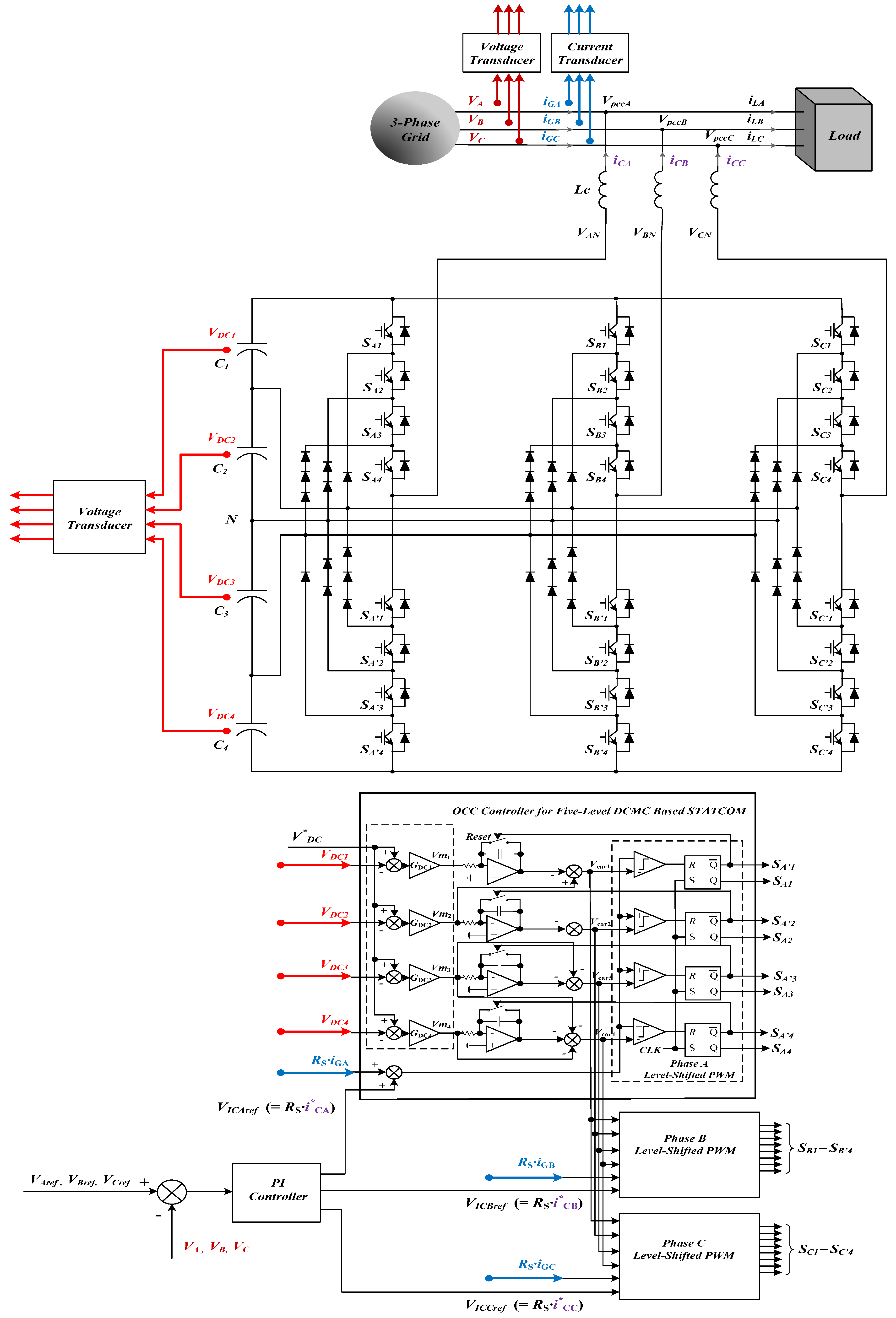
Figure 1 shows a five-level DCMC-based STATCOM configuration. The MV grid is represented by a three-phase voltage source and a three-phase load with the proposed five-level STATCOM connected in the PCC. However, if needed, the STATCOM can also be connected through the step-up transformer to high voltage transmission systems. The proposed five-level STATCOM system is comprised of three main parts: a five-level DCMC, a set of coupling inductors or a step-up transformer, and a STATCOM controller. First, the five-level DCMC has four dc-link capacitors (C1-C4) to produce a five-level output phase voltage (VAN). In each phase leg, there are four complementary main switches (SA1-SA4 and SA’1-SA’4 for the phase-A leg, SB1-SB4 and SB’1-SB’4, and etc.). The voltage stress of each main switch is limited to one dc-link capacitor voltage (VDC/4) thanks to the clamping diodes. Second, the main purpose of the coupling inductors is to filter out the harmonic components of the injected reactive current, which are generated by the pulsating output voltage of the five-level DCMC. Third, the STATCOM controller performs reactive power compensation by controlling the gate signals of the main switches, based on the measured grid phase voltages, grid phase currents, and dc-link capacitor voltages.
The proposed control method of the five-level DCMC-based STATCOM is based on injecting the compensation current into the power grid using the OCC controller. To derive the multi-carrier level-shifted OCC control equation of the five-level DCMC-based STATCOM, the main principle of the OCC method for a two-level voltage source converter (VSC) is reviewed first. For the three-phase two-level VSC, the relationship between the duty ratios of the VSC switches and the grid phase voltages can be defined as follows [25]:
[ 2 3 1 3 1 3 1 3 2 3 1 3 1 3 1 3 2 3 ] [ d S A d S B d S C ] = 1 V D C [ V A V B V C ]
where dSA’, dSB’, dSC’ are the duty ratios of the bottom switches (SA’, SB’, SC’) in the two-level VSC and VDC is the dc bus voltage, and VA, VB, VC are the grid phase voltages.
One possible solution for (1), containing singular matrix and thus having no unique solution can be defined as follows:
[ d S A d S B d S C ] = K 1 + K 2 V D C [ V A V B V C ]
Assume K2 = −1, then from 0 ≤ d ≤ 1, K1 can be defined as:
V A V D C K 1 1 + V A V D C
where VA/VDC is a modulation index and for the three-phase VSC with sinusoidal PWM, its maximum value is equal to 1/ 3 . Thus, based on the defined K1 and K2, (2) can be rewritten by:
[ d S A d S B d S C ] = 1 3 1 V D C [ V A V B V C ]
The control goal of the reactive compensation for the STATCOM is to realize the following relationship between the grid phase voltages and the grid phase currents to achieve power factor correction (PFC) operation for the power grid by the reactive currents of the STATCOM:
[ i G A + i C A * i G B + i C B * i G C + i C C * ] = 1 R E [ V A V B V C ]
where RE is the emulated resistance, VA, VB, VC are the grid phase voltages and iGA, iGB, iGC are the grid phase currents, and i*CA~i*CC are the STATCOM current references which can be defined as follows:
[ i C A * i C B * i C C * ] = j G R [ V A V B V C ] = ( K P + K I s ) [ Δ V p c c A Δ V p c c B Δ V p c c C ]
where GR is the reference conductance related to the voltage fluctuation at the point of the STATCOM connection, KP and KI are the proportional and integral coefficients related to the grid impedances, and ΔVpccA, ΔVpccB, ΔVpccC are the voltage variations at the PCC.
Combining (4) and (5) yields the control key equation of the three-phase two-level STATCOM, of which the reactive compensation strategy can be achieved by controlling the VSC switches in such a way that the duty ratios, the grid phase currents, and the compensation currents satisfy the following equation:
[ R S i G A + V I C A r e f R S i G B + V I C B r e f R S i G C + V I C C r e f ] = V m [ 1 3 d S A 1 3 d S B 1 3 d S C ]
where Vm = VDC RS/ 3 RE, RS is the sensing resistance of the grid phase current and iGA, iGB, iGC are the grid phase currents, and VICjref = RS · i*Cj at j = A, B, C.
In (7), the emulated resistance (RE) of the STATCOM system is adjusted by the duty ratios of the bottom switches in the two-level VSC during each switching cycle to keep the dc bus voltage (VDC) at the constant level.
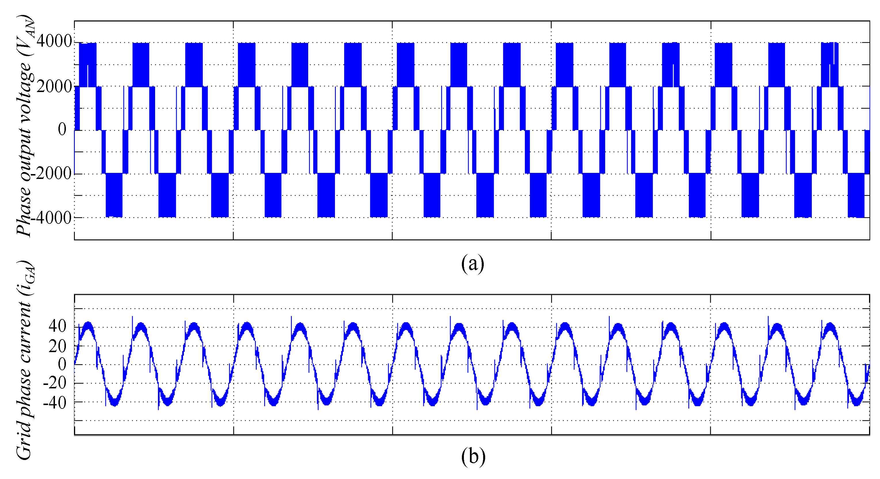
A similar approach is developed for the higher-level DCMC-based STATCOMs with the level-shifted carrier signals. For the five-level DCMC-based STATCOM, four level-shifted carrier signals (Vcar1-Vcar4) are arranged so that they fully occupy contiguous bands in the range of (−VDC3VDC4) to (VDC1 + VDC2). The three-phase sinusoidal control references are then compared with these carrier signals to determine the switched voltage level. The five-level STATCOM is switched to (VDC1 + VDC2) when the control reference is greater than four carrier signals by switching the first upper switch (SA1, SB1, SC1) and its complementary switch (SA’1, SB’1, SC’1). Then the STATCOM is switched to +VDC2 when the control reference is greater than three lower carrier signals (Vcar2, Vcar3, Vcar4) but less than the upper carrier signal (Vcar1) by switching the second upper switch (SA2, SB2, SC2) and its complementary switch (SA’2, SB’2, SC’2). The STATCOM is switched to zero (N) when the control reference is greater than two lower carrier signals (Vcar3, Vcar4) but less than two upper carrier signals (Vcar1, Vcar2) by switching the third upper switch (SA3, SB3, SC3) and its complementary switch (SA’3, SB’3, SC’3). Similarly, the STATCOM is switched to −VDC3 when the control reference is greater than the lower carrier signal (Vcar4) but less than three upper carrier signals (Vcar1, Vcar2, Vcar3) by switching the fourth upper switch (SA4, SB4, SC4) and its complementary switch (SA’4, SB’4, SC’4). Finally, the STATCOM is switched to (−VDC3VDC4) when the control reference is less than four carrier signals.
Based on the above five-level carrier-based modulation, the control key equation of the three-phase five-level STATCOM can be represented by the following equations:
[ R S i G A + V I C A r e f R S i G B + V I C B r e f R S i G C + V I C C r e f ] = V m 1 [ 1 3 d S A 1 1 3 d S B 1 1 3 d S C 1 ] = V m 2 [ 1 3 d S A 2 1 3 d S B 2 1 3 d S C 2 ] = V m 3 [ 1 3 d S A 3 1 3 d S B 3 1 3 d S C 3 ] = V m 4 [ 1 3 d S A 4 1 3 d S B 4 1 3 d S C 4 ]
where Vm1-Vm4 are the carrier amplitudes of four level-shifted carrier signals, depending on each dc-link capacitor voltage (VDC1-VDC4), RS is the sensing resistance of the grid phase current and iGA, iGB, iGC are the grid phase currents, and VICjref = RS · i*Cj at j = A, B, C.
For the three-phase five-level DCMC-based STATCOM, the OCC control equation can be expressed as follows:
[ R S i G A + V I C A r e f R S i G B + V I C B r e f R S i G C + V I C C r e f ] = V m j [ 1 3 d S A j 1 3 d S B j 1 3 d S C j ]
where j = 1,2,3,4 and Vmj = VDCj RS/ 3 RE, and dSA’j, dSB’j, dSC’j are the duty ratios of the bottom switches in the three-phase five-level DCMC-based STATCOM.
Figure 2 shows the proposed level-shifted OCC control of the five-level DCMC-based STATCOM, based on (9). The three sinusoidal control references are compared with four level-shifted carrier signals (Vcar1-Vcar4) to determine the output voltage levels for each phase: (VDC1 + VDC2), +VDC2, 0, −VDC3, (−VDC3VDC4). The eight main switches per phase are controlled as complementary pairs (SA1, SA’1, etc.). As shown in Figure 2, the first upper carrier signal Vcar1 has Vm1 amplitude and determines the switching status of the first upper switch (SA1, SB1, SC1) and its complementary switch (SA’1, SB’1, SC’1). Similarly, the second upper carrier signal Vcar2 has Vm2 amplitude and decides the switching status of the second upper switch (SA2, SB2, SC2) and its complementary switch (SA’2, SB’2, SC’2). For the other two carrier signals (Vcar3, Vcar4), the same control approach is applied to determine the switching condition of the related main switches.
For the sinusoidal control reference of Phase-A, the line period is divided into four operation regions, according to where the control reference signal lands, named as I, II, III, and IV.
Table 1 shows the five-level STATCOM output voltages (VAN) and their switching states of Phase A. In region I in Figure 2, the STATCOM output voltage is switched between VDC1 + VDC2 and VDC2 by the first upper switch SA1 and its complementary switch SA’1. In addition, the other upper switches (SA2-SA4) are kept on in region I. Similarly, in region II, the second upper switch SA2 and its complementary switch SA’2 are switched to provide the STATCOM output voltage between VDC2 and 0. In this region, the first upper switch SA1 is turned off, and the other two upper switches (SA3, SA4) are always turned on to provide the neutral point connection (0 or N) in Figure 1. For region III and IV, the same switching approach is applied to produce the negative STATCOM output voltages. From Section 2, the control key equations of the five-level DCMC-based STATCOM for four operation regions of Phase A can be derived in Table 2.

3. OCC Controller for DCMC-Based STATCOMs

The proposed OCC controller for the five-level DCMC-based STATCOM is shown in Figure 3. The four-carrier level-shifted OCC controller is realized using a clock signal (CLK), four integrators, four comparators, four RS flip-flops, and four reset switches for PWM generation. The four-channel voltage compensators and the level-shifted carrier generators produce four carrier ramps and four level-shifted carrier signals. In detail, the four identical voltage compensators (GDC1-GDC4) determine four carrier amplitudes (Vm1-Vm4) depending on deviation of each dc-link capacitor voltage (VDC1-VDC4) from the reference voltage V*DC (=VDC/4). To compensate the dc-link capacitor voltage variations, the equivalent STATCOM resistance (RE) is adjusted by each carrier amplitude (Vm1-Vm4) in (9).
The transfer function of the four identical voltage compensators GDCi(s) can be obtained as follows [26]:
G D C i ( s ) = Δ V m i Δ V D C i = K m i ( 1 + s ω z m i ) s ( 1 + s ω p m i )
where Kmi is the proportional coefficient, ωzmi is the zero far below the zero crossover frequency, and ωpmi is the pole located right at the zero crossover frequency.
Using the four integrators with reset and three adders, the four level-shifted carrier signals (Vcar1-Vcar4) are generated with the different amplitudes and dc-level shifts. The proposed level-shifted carrier signals can be respectively represented as follows:
V c a r 1 ( t ) = V m 1 T S t + V m 2
V c a r 2 ( t ) = V m 2 T S t
V c a r 3 ( t ) = V m 3 T S t V m 3
V c a r 4 ( t ) = V m 4 T S t ( V m 3 + V m 4 )
where 0 < tTS, TS is the period of the carrier signals, and Vm1-Vm4 are the amplitudes of the four carrier signals.
The maximum amplitude of the four carrier signals can be decided by the supply voltage or the maximum differential input voltage of the comparators. Since the maximum input voltage of the (−) input terminal (Vcar1) of the first upper comparator in Figure 3 is (Vm1 + 
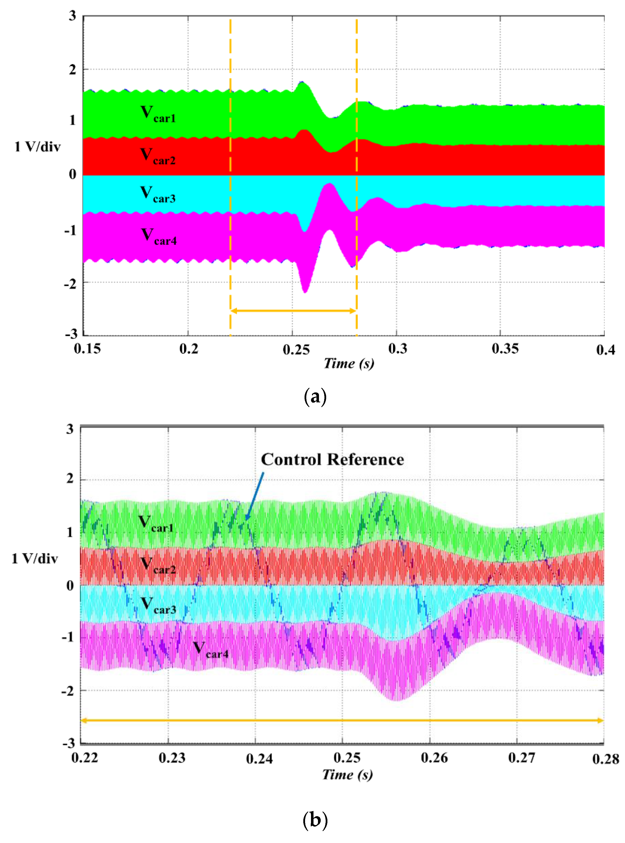
Vm2), one-quarter of the supply voltage can be selected for the maximum amplitude of the four carrier signals. For example, if the supply voltage of the comparators is ±15 V~±18 V, the maximum amplitude of the four carrier signals is 3.75 V~4.5 V. The minimum amplitude of the four carrier signals can be the minimum output voltage of the op-amps in the OCC controller or zero. When the amplitude of the carrier signal reaches its minimum value, the voltage control of the related dc-link capacitor by the carrier signal is somewhat limited during minimum value operation cycles but the total dc-link capacitor voltage balancing would be continuously handled by the other carrier signals and dc-link capacitors.
The resulting level-shifted carrier signals (Vcar1-Vcar4) with variable amplitudes and dc-level shifts are shown in Figure 2. When the four dc-link capacitor voltages (VDC1-VDC4) are out of balance due to any reason or there are dynamic load changes, the four-channel voltage compensators continuously adjust the amplitudes of the four carrier signals (Vm1-Vm4) to stabilize each dc-link capacitor voltage based on the reference voltage (VDC/4). In addition, OCC double-edge modulation can be also used in the proposed OCC controller for the DCMC-based STATCOM to provide high-quality output voltage with reduced harmonics.
With the proposed variable amplitude control of the carrier signals, each dc-link capacitor voltage can be properly balanced and equal to the reference voltage even under different dc-link capacitances (C1-C4). The actual duty ratios of the main switches for the phase-A leg (SA1-SA’4) are achieved by comparing the control reference (RS·iGA + VICAref) with the four level-shifted carrier signals in the level-shifted PWM block. When the amplitude of the carrier signals reaches its maximum value, the voltage control capability of the related dc-link capacitors is limited, including overmodulation condition.
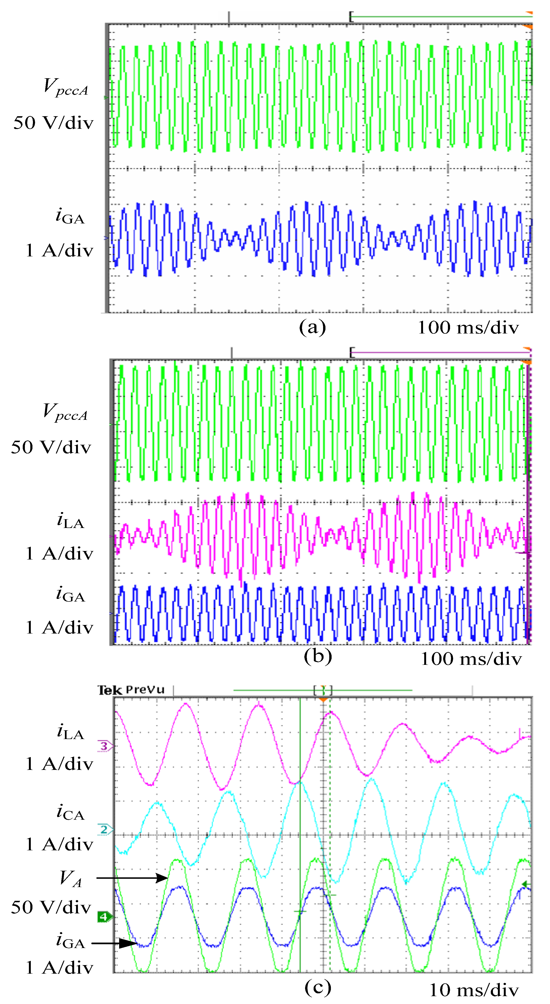
The control system of the five-level DCMC-based STATCOM is shown in Figure 4. The proposed level-shifted OCC controller produces the control references for the current control loop and generates the gate signals for the five-level STATCOM. In addition, the voltage control loop generates the STATCOM current references for the reactive compensation which is implemented with proportional and integral (PI) control algorithm. For voltage regulation in the power system, the reactive power compensation is realized by controlling the injected or absorbed reactive current of the five-level STATCOM.
Assuming that there is a voltage sag (+ΔVpccA) in Phase A, the five-level STATCOM tries to regulate the grid voltage and make it come back to normal. From the multilevel OCC control Equation (9) of the five-level STATCOM, the following control equations can be derived to compensate the voltage sag and regulate the grid voltage within the standard.
In region I of Figure 2, since the STATCOM output voltage is only switched between VDC1 + VDC2 and VDC2 by the first upper switch SA1 and the other upper switches (SA2-SA4) are kept on from Table 1, the voltage regulation is only controlled by the first upper switch SA1 in region I as follows:
R S i G A + ( K P + K I s ) ( V A r e f V A ) = R S i G A + ( K P + K I s ) ( + Δ V p c c A ) = V m 1 ( 1 3 d S A 1 )
From above, the duty ratios of the first upper switch SA1 (dSA1) and its complementary switch SA’1 (dSA’1) can be derived as follows:
d S A 1 = 1 3 1 3 V m 1 [ R S i G A + ( K P + K I s ) ( + Δ V p c c A ) ]
d S A 1 = 1 d S A 1 = ( 1 1 3 ) + 1 3 V m 1 [ R S i G A + ( K P + K I s ) ( + Δ V p c c A ) ]
From (17), it is clear that the duty ratio of the first upper switch SA1 (dSA1) increases by the voltage sag (+ΔVpccA) in Phase A and the STATCOM output voltage (VAN) can be increased by the duty ratio (dSA1) to inject the reactive power into the power grid for the voltage regulation.
In region II, since the second upper switch SA2 and its complementary switch SA’2 are only switched to provide the STATCOM output voltage between VDC2 and 0 as shown in Table 1, the voltage regulation is achieved by the second upper switch SA2 in region II as follows:
R S i G A + ( K P + K I s ) ( V A r e f V A ) = R S i G A + ( K P + K I s ) ( + Δ V p c c A ) = V m 2 ( 1 3 d S A 2 )
Similarly, the duty ratios of the second upper switch SA2 (dSA2) and its complementary switch SA’2 (dSA’2) can be expressed as follows:
d S A 2 = 1 3 1 3 V m 2 [ R S i G A + ( K P + K I s ) ( + Δ V p c c A ) ]
d S A 2 = 1 d S A 2 = ( 1 1 3 ) + 1 3 V m 2 [ R S i G A + ( K P + K I s ) ( + Δ V p c c A ) ]
From (20), it is also clear that the duty ratio of the second upper switch SA2 (dSA2) increases by the voltage sag (+ΔVpccA) in Phase A and the STATCOM output voltage (VAN) can be also increased by the duty ratio (dSA2) to inject the reactive power for the voltage regulation in region II.
In addition, the voltage regulation of the proposed STATCOM in region II can be also explained by Table 2. In region II, the control key equation of the STATCOM is given by:
R S i G A + V I C A r e f = R S i G A + ( K P + K I s ) ( + Δ V p c c A ) = V m 2 d S A 2
From above, the duty ratio of the second upper switch SA2 (dSA2) can be expressed as follows:
d S A 2 = 1 V m 2 [ R S i G A + ( K P + K I s ) ( + Δ V p c c A ) ]
From (22), when there is the voltage sag (+ΔVpccA) in Phase A, the STATCOM output voltage (VAN) can be increased by the duty ratio (dSA2) to inject the reactive power into the power grid for the voltage regulation in region II.
For the diode-clamped multilevel converters, a major challenge is to keep all dc-link capacitor voltages balanced, which was achieved with an extra voltage-balancing circuitry or a specific voltage-balancing control previously. For example, a modified SPWM method was proposed in [17] in order to balance the two dc-link capacitor voltages for the three-level diode-clamped inverters. It is based on changing the boundary offset on the middle point of two carrier signals, which can control the neutral-point current to ensure balanced dc-link capacitor voltages. However, the main drawback in this approach is the restricted stability in order to obtain a simple control strategy.
Figure 5 shows the proposed four-carrier level-shifted OCC control algorithm of the proposed five-level STATCOM to maintain the dc-link capacitor voltage balance in region I and II.
For the detailed analysis of the dc-link capacitor voltage balance, the two dc-link capacitor currents (iC1, iC2) in region I can be described by the following expressions:
i C 1 = C 1 d V D C 1 d t = i C H A 1 i D I S 1
i C 2 = C 2 d V D C 2 d t = i C 1 + i C H A 2 i D I S 2
Similarly, the two dc-link capacitor currents in region II can be expressed as:
i C 1 = C 1 d V D C 1 d t = i D I S 1
i C 2 = C 2 d V D C 2 d t = i C 1 + i C H A 2 i D I S 2
Assuming that the four dc-link capacitors (C1-C4) have the same capacitance, when a disturbance causes imbalance in the two upper dc-link capacitor voltages (VDC1 > V*DC > VDC2), a state variable ∆V is defined as half the difference between the two upper dc-link capacitor voltages (VDC1, VDC2), which should converge to zero with the proposed OCC control. In the unbalanced condition, each dc-link capacitor voltage can be defined as a function of the voltage difference ∆V by:
V D C 1 = V C + Δ V
V D C 2 = V C Δ V
where
V C = V D C 1 + V D C 2 2
Δ V = V D C 1 V D C 2 2
In order to maintain the dc-link capacitor voltage balance, the proposed control of the five-level STATCOM in region I and II is shown in Figure 5. From Figure 5a, the duty ratios of the SA1 switch under an unbalanced dc-link condition can be described as follows:
d S A 1 ( n ) = T d S A 1 ( n ) T S = R S i G A + V I C A r e f V m 2 V m 1
d S A 1 ( n + 1 ) = T d S A 1 ( n + 1 ) T S = R S i G A + V I C A r e f ( V m 2 Δ V m 2 ) V m 1 + Δ V m 1
where dSA1(n) and dSA1(n+1) are the duty ratios of the SA1 switch at the (n)th and (n + 1)th switching cycles, and
V m 1 = V D C 1 R S 3 R E
Δ V m 1 = R S 3 R E Δ V D C 1 = R S 3 R E Δ V
From (27) and (28), the duty ratio variation of the SA1 switch (∆dSA1) to compensate the unbalanced dc-link capacitor voltages can be obtained by:
Δ d S A 1 = d S A 1 ( n + 1 ) d S A 1 ( n ) = Δ V D C 1 ( n ) [ R E ( i G A + i C A * ) + V D C 2 ( n ) ] + Δ V D C 2 ( n ) V D C 1 ( n ) V D C 1 ( n ) ( V D C 1 ( n ) + V D C 2 ( n ) ) V D C 1 ( n ) ( V D C 1 ( n ) + Δ V D C 1 ( n ) )
Assuming VDC1(n) >> ∆VDC1(n), the above equation can be simplified as:
Δ d S A 1 = Δ V D C 1 ( n ) V D C 1 ( n ) 2 [ R E ( i G A + i C A * ) + V D C 2 ( n ) ] + Δ V D C 2 ( n ) V D C 1 ( n ) ( V D C 1 ( n ) + V D C 2 ( n ) ) V D C 1 ( n )
From (23) and (30), it is possible to define the relationship between the duty ratio variation of the Vcr1 carrier signal and the compensation for the dc-link capacitor voltage unbalance. The voltage variations of the two upper dc-link capacitors (C1, C2) in region I are given by:
Δ V D C 1 ( n + 1 ) = T S C 1 V D C 1 ( n ) 2 [ R E ( i G A + i C A * ) + V D C 2 ( n ) ] ( i G A + i C A * ) Δ V D C 1 ( n ) + T S C 1 V D C 1 ( n ) ( i G A + i C A * ) Δ V D C 2 ( n ) T S C 1 V D C 1 ( n ) ( V D C 1 ( n ) + V D C 2 ( n ) ) ( i G A + i C A * ) T S C 1 Δ I D I S 1 = A 1 Δ V D C 1 ( n ) + A 2 Δ V D C 2 ( n ) + A C 1 + A C 2
Δ V D C 2 ( n + 1 ) = T S C 2 ( Δ I D I S 1 Δ I D I S 2 ) = B C 1 + B C 2
When VDC1 > V*DC > VDC2, ∆dSA1 is negative and ∆IDIS1 is positive in region I. Therefore, the over-charged C1 capacitor voltage (VDC1) will decrease and the under-charged or over-discharged C2 capacitor voltage (VDC2) will increase to reduce the dc-link capacitor voltage deviation, depending on the difference between ∆IDIS1 and ∆IDIS2. In this unbalanced condition, ∆VDC1 is decreasing during each switching cycle to reach the nominal dc-link capacitor voltage.
Since ∆VDC1(n) − ∆VDC1(n+1) = (1 − A1)·∆VDC1(n)A2·VDC2(n)AC1AC2 > 0, the following compensation control is obtained:
Δ V D C 1 ( n + 1 ) Δ V D C 1 ( n ) < 1
In this unbalanced condition, ∆VDC1 is decreasing during each switching cycle to reach the nominal dc-link capacitor voltage. From Figure 5b, similarly, the duty ratios of the SA2 switch under an unbalanced dc-link condition can be described as follows:
d S A 2 ( n ) = T d S A 2 ( n ) T S = R S i G A + V I C A r e f V m 2
d S A 2 ( n + 1 ) = T d S A 2 ( n + 1 ) T S = R S i G A + V I C A r e f V m 2 Δ V m 2
where dSA2(n) and dSA2(n+1) are the duty ratios of the SA2 switch at the (n)th and (n + 1)th switching cycles, and
V m 2 = V D C 2 R S 3 R E
Δ V m 2 = R S 3 R E Δ V D C 2 = R S 3 R E Δ V
From (33) and (34), the duty ratio variation of the SA2 switch (∆dSA2) to adjust the unbalanced dc-link capacitor voltages can be obtained by:
Δ d S A 2 = d S A 2 ( n + 1 ) d S A 2 ( n ) = Δ V D C 2 ( n ) R E ( i G A + i C A * ) V D C 2 ( n ) ( V D C 2 ( n ) Δ V D C 2 ( n ) )
Assuming VDC2(n) >> ∆VDC2(n), the duty ratio variation of the SA2 switch can be simplified as:
Δ d S A 2 = d S A 2 ( n + 1 ) d S A 2 ( n ) = Δ V D C 2 ( n ) V D C 2 ( n ) 2 R E ( i G A + i C A * )
From (24) and (36), the voltage variations of the two upper dc-link capacitors (C1, C2) in region II are given by:
Δ V D C 1 ( n + 1 ) = T S C 1 ( Δ I D I S 1 ) = A C 2
Δ V D C 2 ( n + 1 ) = T S C 2 V D C 2 ( n ) 2 R E ( i G A + i C A * ) 2 Δ V D C 2 ( n ) T S C 2 ( Δ I D I S 1 + Δ I D I S 2 ) = B 2 Δ V D C 2 ( n ) + B C 1 + B C 2
When VDC1 > V*DC > VDC2, ∆dSA2 is positive and ∆IDIS1 is also positive in region II, the over-charged C1 capacitor voltage (VDC1) will decrease and the under-charged C2 capacitor voltage (VDC2) will increase to eliminate the dc-link capacitor voltage deviation.
Finally, the voltage variations of the four dc-link capacitors (C1-C4) can be described as follows:
[ Δ V D C 1 ( n + 1 ) Δ V D C 2 ( n + 1 ) Δ V D C 3 ( n + 1 ) Δ V D C 4 ( n + 1 ) ] = [ T S C 1 V D C 1 ( n ) 2 [ R E ( i G A + i C A * ) + V D C 2 ( n ) ] ( i G A + i C A * ) T S C 1 V D C 1 ( n ) ( i G A + i C A * ) 0 0 0 T S C 2 V D C 2 ( n ) 2 R E ( i G A + i C A * ) 2 0 0 0 0 T S C 3 V D C 3 ( n ) 2 R E ( i G A + i C A * ) 2 0 0 0 T S C 4 V D C 4 ( n ) ( i G A + i C A * ) T S C 4 V D C 4 ( n ) 2 [ R E ( i G A + i C A * ) + V D C 3 ( n ) ] ( i G A + i C A * ) ] [ Δ V D C 1 ( n ) Δ V D C 2 ( n ) Δ V D C 3 ( n ) Δ V D C 4 ( n ) ] + [ T S C 1 V D C 1 ( n ) ( V D C 1 ( n ) + V D C 2 ( n ) ) ( i G A + i C A * ) T S C 1 Δ I D I S 1 T S C 2 Δ I D I S 1 T S C 2 Δ I D I S 2 T S C 3 Δ I D I S 3 T S C 3 Δ I D I S 4 T S C 4 V D C 4 ( n ) ( V D C 3 ( n ) + V D C 4 ( n ) ) ( i G A + i C A * ) T S C 4 Δ I D I S 4 ] = [ A 1 A 2 0 0 0 B 2 0 0 0 0 C 3 0 0 0 D 3 D 4 ] [ Δ V D C 1 ( n ) Δ V D C 2 ( n ) Δ V D C 3 ( n ) Δ V D C 4 ( n ) ] + [ A C 1 + A C 2 B C 1 + B C 2 C C 1 + C C 2 D C 1 + D C 2 ] = [ A 1 A 2 0 0 0 B 2 0 0 0 0 C 3 0 0 0 D 3 D 4 ] [ Δ V D C 1 ( n ) Δ V D C 2 ( n ) Δ V D C 3 ( n ) Δ V D C 4 ( n ) ] + [ A C B C C C D C ]
Using (38), the voltage variation vector ΔVDC(n) can be written by a 4 × 4 matrix A and the initial voltage variation vector ΔVDC(0):
Δ V D C ( n ) = [ Δ V D C 1 ( n ) Δ V D C 2 ( n ) Δ V D C 3 ( n ) Δ V D C 4 ( n ) ] = A [ Δ V D C 1 ( n 1 ) Δ V D C 2 ( n 1 ) Δ V D C 3 ( n 1 ) Δ V D C 4 ( n 1 ) ] + B = A n [ Δ V D C 1 ( 0 ) Δ V D C 2 ( 0 ) Δ V D C 3 ( 0 ) Δ V D C 4 ( 0 ) ] + C = A n Δ V D C ( 0 ) + C
where
A n = [ A 1 n ( A 1 n 1 + A 1 n 2 B 2 + + A 1 B 2 n 2 + B 2 n 1 ) A 2 0 0 0 B 2 n 0 0 0 0 C 3 n 0 0 0 ( C 3 n 1 + C 3 n 2 D 4 + + C 3 D 4 n 2 + D 4 n 1 ) D 3 D 4 n ] and   C = [ A n + A n 1 + A + I ] · B
From (38)–(40), it is clear that the voltage variations of the four dc-link capacitors become zero in steady state, even though there are some voltage variations of the dc-link capacitors in the beginning or induced by some perturbation. Based on the proposed four-carrier level-shifted OCC control, dc-link capacitor voltage balance can be successfully achieved. It is also clear that the stabilizing time required to eliminate the dc-link voltage unbalance is proportional to the dc-link capacitance and inversely proportional to the amplitude of the input current. However, the proposed multilevel OCC controller may have limited control capability of the dc-link voltage balance during AC network failures since the low AC voltage over a long period prevents the proposed multilevel OCC controller from switching the first upper switches in region I to control the upper dc-link capacitor (C1) voltage. During the low AC voltage condition, the proposed multi-carrier level-shifted OCC control loses its controllability of the dc-link voltage balance.
For region III and IV, the same control approach is applied to regulate the grid voltage from the voltage variation at the PCC, for example, the voltage sag (or swell). Finally, it is concluded that the voltage variation (sag or swell) can be automatically compensated by the proposed five-level STATCOM with the multilevel OCC controller for all operation regions.

4. Simulation and Experimental Results

4.1. Simulation Results

The proposed five-level DCMC-based STATCOM with the OCC controller for reactive power compensation has been verified by simulation using MATLAB/Simulink. The simulation circuit model presented in Figure 6 is composed of: a three-phase voltage source (VA, VB, VC), two three-phase RL-loads (R1L1, R2L2), and the shunt-connected five-level DCMC-based STATCOM with coupling inductors (Lc). IGBTs are used for the main switches of the proposed STATCOM.
The parameters of the simulation circuit are as follows: VA, VB, VC = 4.16 kV/ 3 (rms), R1 = 150 Ω, R2 = 300 Ω, L1 = 350 mH, and L2 = 250 mH. The dc bus voltage (VDC) is 8 kV and the reference voltage (V*DC) of each dc-link capacitor voltage (VDC1-VDC4) is 2 kV. The dc-link capacitors (C1-C4) have the different capacitances to emulate the voltage unbalance: C1 = 1.3 mF, C2 = 1.1 mF, C3 = 0.8 mF, and C4 = 0.9 mF. The grid line frequency is 60 Hz and the carrier frequency is 5 kHz. The grid impedance is considered as 0.001 Ω–0.5 mH. The main parameters of the simulation circuit model are listed in Table 3.
To simulate the dynamic behavior of the proposed STATCOM, at the time moment tC = 0.25 s, the load change switches S1 and S2 are commutated to change the load from the R1L1 to the R2L2 load.
Figure 7 shows the simulation waveforms of the STATCOM line-to-line output voltage (Figure 7a) and phase output voltage (Figure 7b). As can be seen, the phase output voltage has five output voltage levels and the voltage step is equal to the reference voltage 2 kV, as the line-to-line voltage has nine output voltage levels with the same voltage step.
Figure 8 shows the four voltage waveforms across the dc-link capacitors with the proposed OCC balancing technique. It is shown that when the load has a step transient, the four dc-link capacitor voltages of the proposed DCMC-based STATCOM are equally balanced in dynamic state even under unequal dc-link capacitances.
Figure 9 shows the four level-shifted carrier signals (Vcar1-Vcar4) with variable amplitudes and dc-level shifts determined by Vm1-Vm4 values. Unlike the conventional approaches with multi-carrier level-shifted PWM control, the amplitudes of the four carrier signals (Vm1-Vm4) in the proposed level-shifted OCC controller vary in such a way to stabilize the dc-link capacitor voltages and provide reactive power compensation in accordance with (9). By comparing the control reference with the four carrier signals, the actual gate signals are produced by the RS flip-flops. With variable amplitude control of the four carrier signals, the dc-link capacitor voltages can become balanced and equal to the reference voltage (VDC/4) even under different dc-link capacitances (C1-C4). During dynamic load change, the amplitudes of the four carrier signals become larger first to stabilize the dc-link capacitor voltages since variations of the dc-link capacitor voltages are rapidly increased. Then the amplitudes of the four carrier signals are decreasing to provide smaller reactive power for the light RL-load (R2L2). As shown in Figure 9, the proposed level-shifted OCC controller rapidly regulates the five-level STATCOM operating conditions in response to the step change in the reactive loads. However, the minimum amplitude of the carrier signals impacts on the distortion level of the synthesized multilevel waveforms.
Figure 10 shows the simulation waveforms of the proposed five-level STATCOM with the multilevel OCC control. The grid phase voltage (VA), the load current (iLA), the STATCOM current (iCA), the grid phase current (iGA), and the two upper dc-link capacitor currents (iC1, iC2) are shown in Figure 10 when the load has a step transient. As shown in Figure 10e,f, the two dc-link capacitor currents (iC1, iC2) have the balanced and proper current direction, following the STATCOM current (iCA). Since the first upper switch SA1 is turned off and the second upper switch SA2 is switched to provide the STATCOM output voltage between VDC2 and 0 in region II of Figure 2, the second upper dc-link capacitor current (iC2) only has the continuous current flow to generate the STATCOM current (iCA) in region II.
With reactive power compensation by the proposed multilevel OCC STATCOM, the grid phase current is in phase with the grid phase voltage and during dynamic load change, the dc-link capacitor voltages can become balanced with the stabilized dc-link capacitor currents (iC1, iC2) even under different dc-link capacitances (C1-C4).
Figure 11 shows the simulation waveforms of the proposed five-level STATCOM with a three-phase diode rectifier load to verify the effectiveness of the proposed multilevel OCC control method under nonlinear load conditions. In Figure 11, the same simulation model and parameters in Table 3 have been used except the three-phase diode rectifier, which is connected to the single-phase RL-load (R1L1). As shown in Figure 11, the four dc-link capacitor voltages (VDC1-VDC4) of the proposed DCMC-based STATCOM with unequal dc-link capacitances are stably balanced (2 kV) even under the diode rectifier load condition, which produces severe harmonic voltage disturbance in the power grid system. When the proposed DCMC-based STATCOM is enabled and connected to the PCC, the highly distorted grid phase current (iGA) with 27.1% total harmonic distortion (THD) becomes sinusoidal with 8.1% THD.
Figure 12 and Figure 13 show the effectiveness of the proposed multilevel OCC control method on source-side voltage sag and swell conditions. The same simulation model and parameters in Figure 6 have been used except the voltage sag or swell condition of the grid phase voltage (VA) from the time moment t = 0.40 s to t = 0.45 s (3 cycles). To emulate the voltage sag and swell conditions, 0.2 pu voltage decrease in Figure 12 and 0.2 pu voltage increase in Figure 13 have been considered. As shown in Figure 12 and Figure 13, the four dc-link capacitor voltages (VDC1-VDC4) of the proposed DCMC-based STATCOM with unequal dc-link capacitances are stably balanced even under the voltage sag and swell conditions.

4.2. Experimental Results

A 2 kVA five-level DCMC-based STATCOM prototype was built in Figure 14 for performance verification. As the main switches, IGBTs (IRGP4072DPbF) with 2.5 A optocoupler gate drivers (VO3120) were used in the prototype. In addition, ultrafast diodes (MUR1520) were also applied to the STATCOM prototype as the clamping diodes. The three-phase grid phase voltage (VA, VB, VC) is 120 V and adjustable by a three-phase variable transformer (TV). The dc bus voltage (VDC) is 400 V and each dc-link capacitor (C1-C4) is 2.72 mF. Three 2.8 mH coupling inductors (Lc) are used to connect the proposed STATCOM to the power grid. The grid line frequency is 60 Hz and the carrier frequency is 5 kHz, which are the same frequencies in simulation. The sensing resistance (RS) of the grid phase current is 0.5 Ω. For dc-link voltage measurement, four isolation amplifiers (AD202KN) are used to sense each dc-link capacitor voltage (VDC1-VDC4) with 0.02 V/V gain. Based on discrete analog circuit, the proposed multilevel OCC controller is implemented. To realize a simple and flexible controller, field programmable analog arrays (FPAAs) can be used to implement the analog multilevel OCC controller. The main parameters of the experimental system are listed in Table 4.
In the test, a 1 kW 1800 rpm three-phase synchronous motor was used as an inductive load. Figure 15 shows the system configuration under the test.
It consists of the three-phase variable transformer, the synchronous motor (SM), the five-level DCMC-based STATCOM with the proposed level-shifted OCC controller, and phase current sensors (CSA-CSC). The proposed STATCOM is connected to the point of the motor connection via the coupling inductors, as shown in Figure 15.
The line-to-line output voltage of the proposed five-level DCMC-based STATCOM is shown in Figure 16. As can be seen, the line-to-line voltage of the proposed STATCOM has nine output voltage levels with 50 V voltage step. In this test condition, the dc-link voltage is 200 V and equally shared by the four dc-link capacitors (C1-C4).
Figure 17 shows that the four dc-link capacitor voltages of the proposed five-level DCMC-based STATCOM can keep balanced in steady state. During operation, each capacitor voltage is automatically maintained by the voltage compensator without additional voltage-balancing hardware.
Figure 18 shows the experimental waveforms in the transient state when the load is changed from a resistive to inductive load. In this test condition, the three-phase grid phase voltage (VA, VB, VC) is 120 V and the dc-link voltage is 380 V, which is equally shared by the four dc-link capacitors (C1-C4) at the beginning of the operation. Since the initial load is purely resistive (RO), the load only consumes the active power, 1.8 kW and the proposed STATCOM delivers no reactive power. To evaluate the dynamic performance of the proposed STATCOM, the load change is made from RO to RO + oLO load. In this case, the inductive load consumes 1 kVAR reactive power (Q*). For the proposed OCC controller, the overall control goal is that if the voltage at the PCC is within the standard, the STATCOM will work to improve the power factor for the power grid or if the voltage at the PCC is out of the standard limitation, the STATCOM will regulate the voltage at the PCC.
As shown in Figure 18, the proposed five-level STATCOM provides satisfactory operating performance, including unity power factor for the power grid and dc-link capacitor voltage (VDC1-VDC4) regulation in the steady and transient states. However, since some high harmonics are injected from the three-phase variable transformer (TV), the experimental results in Figure 18a show the distorted voltage and current waveforms.
Figure 19 shows the experimental waveforms of the grid phase voltage (VA), the load current (iLA), and the grid phase current (iGA). In Figure 19, the load current has some phase delay with the grid phase voltage since the synchronous motor consumes the reactive power, working as a RL load. With reactive power compensation by the proposed STATCOM, the grid phase current is in phase with the grid phase voltage and has smaller amplitude compared with the load current amplitude. Therefore, the proposed STATCOM can provide power factor improvement for the power grid.
The voltage variation is directly related to real and reactive power variations and is commonly classified as voltage sag, voltage swell, short interruption, and long duration voltage variation. The voltage flicker happens when there are dynamic variations in the power system caused by dynamic loads or sources. The amplitude of voltage fluctuation depends on grid strength, network impedance, and phase angle or power factor of the dynamic loads. Huge non-linear industrial loads such as electrical arc furnaces, pumps, welding machines, and rolling mills are known as voltage flicker generators.
In this test, the three-phase synchronous motor is used to create the voltage fluctuation in the power system. When the output voltage of the three-phase variable transformer is under the input voltage rating of the synchronous motor, the stator winding is partially excited and creates a weak rotating magnetic field, which revolves at the designated motor speed. However, the rotor, due to its inertia, could not follow the revolving magnetic field since the intensity of the rotating magnetic field is not enough to overcome the rotor inertia and resistance to the rotation. During this operating condition, the synchronous motor is not fully synchronized and behaves in the form of a variable impedance load which can create the voltage flicker in the power system.
Figure 20 shows the experimental waveforms without and with the proposed five-level DCMC-based STATCOM, operating under dynamic load change. When the synchronous motor operates under the rated input voltage, the unstable rotation of the synchronous motor changes the load current by consuming different active and reactive currents. This operating condition can emulate the dynamic change of the inductive load.
As shown in Figure 20a, there is about 10% periodic voltage variation or voltage flicker at the PCC (VpccA), when the STATCOM is not in operation. In Figure 20b,c, the five-level DCMC-based STATCOM dynamically provides the reactive compensation current (iCA) to eliminate the voltage flicker and keep the constant voltage at the PCC.

5. Conclusions

This paper presents the five-level DCMC-based STATCOM with the OCC controller for power quality improvement or grid voltage stabilization. Simulation and experiments have shown that the proposed five-level OCC DCMC-based STATCOM has excellent steady-state and dynamic performance for power factor improvement and is capable of stabilizing the unstable voltage or voltage flicker at the point of the STATCOM connection. The demonstrated features are very important to stabilize the grid voltage to allow increased penetration of renewable energy resources (e.g., wind).
The proposed OCC voltage-balancing technique of the dc-link capacitors is capable of keeping the dc-link capacitor voltages balanced even when the four dc-link capacitors have different capacitance or initial voltage condition. However, the proposed multilevel OCC controller may have limited control capability of the dc-link voltage balance under low AC voltage conditions. It is suitable for MV high power distribution system applications.

Author Contributions

Conceptualization, methodology, validation, formal analysis, and writing—original draft preparation, I.W.J.; writing—review and editing, and supervision, T.H.S. Both authors have read and agreed to the published version of the manuscript.

Funding

This research received no external funding.

Acknowledgments

This work was supported by the Korea Institute of Energy Technology Evaluation and Planning (KETEP) and the Ministry of Trade, Industry & Energy (MOTIE) of the Republic of Korea. (No. 20192010106790).

Conflicts of Interest

The authors declare no conflict of interest.

Abbreviations

The following abbreviations are used in this manuscript:
OCCOne-cycle control
DCMCDiode-clamped multilevel converter
CMCCascaded multilevel converter
VSCVoltage source converter
STATCOMStatic VAR compensator
MVMedium voltage
IGBTInsulated gate bipolar transistor
IGCTIntegrated gate commutated thyristor
SVPWMSpace vector pulsewidth modulation
PCCPoint of common coupling
PFCPower factor correction
FPAAField programmable analog array

References

  1. Wind Power Becomes More Cost Effective with 340,000 Turbines Already Installed Worldwide by 2016. Available online: https://www.eqmagpro.com/wind-power-becomes-more-cost-effective-with-340000-turbines-already-installed-worldwide-by-2016 (accessed on 12 January 2018).
  2. Fujii, K.; Schwarzer, U.; De Doncker, R.W. Comparison of Hard-Switched Multi-Level Inverter Topologies for STATCOM by Loss-Implemented Simulation and Cost Estimation. In Proceedings of the 2005 IEEE 36th Annual Power Electronics Specialists Conference (PESC), Recife, Brazil, 12–16 June 2005; pp. 340–346. [Google Scholar]
  3. Akagi, H.; Fujita, H.; Yonetani, S.; Kondo, Y. A 6.6-kV Transformerless STATCOM Based on a Five-Level Diode-Clamped PWM Converter: System Design and Experimentation of a 200-V 10-kVA Laboratory Model. IEEE Trans. Ind. Appl. 2008, 44, 672–680. [Google Scholar] [CrossRef]
  4. Chen, B.S.; Hsu, Y.Y. A Minimal Harmonic Controller for a STATCOM. IEEE Trans. Ind. Electron. 2008, 55, 655–664. [Google Scholar] [CrossRef] [Green Version]
  5. Singh, B.; Murthy, S.S.; Gupta, S. STATCOM-Based Voltage Regulator for Self-Excited Induction Generator Feeding Nonlinear Loads. IEEE Trans. Ind. Electron. 2006, 53, 1437–1452. [Google Scholar] [CrossRef]
  6. Saeedifard, M.; Nikkhajoei, H.; Iravani, R. A Space Vector Modulated STATCOM Based on a Three-Level Neutral Point Clamped Converter. IEEE Trans. Power Deliv. 2007, 22, 1029–1039. [Google Scholar] [CrossRef]
  7. Sternberger, R.; Jovcic, D. Theoretical Framework for Minimizing Converter Losses and Harmonics in a Multilevel STAT-COM. IEEE Trans. Power Deliv. 2008, 23, 2376–2384. [Google Scholar] [CrossRef]
  8. Song, Q.; Liu, W. Control of a Cascade STATCOM With Star Configuration Under Unbalanced Conditions. IEEE Trans. Power Electron. 2009, 24, 45–58. [Google Scholar] [CrossRef]
  9. Barrena, J.A.; Marroyo, L.; Vidal, M.Á.R.; Apraiz, J.R.T. Individual Voltage Balancing Strategy for PWM Cascaded H-Bridge Converter-Based STATCOM. IEEE Trans. Ind. Electron. 2008, 55, 21–29. [Google Scholar] [CrossRef]
  10. Cheng, Y.; Qian, C.; Crow, M.L.; Pekarek, S.; Atcitty, S. A Comparison of Diode-Clamped and Cascaded Multilevel Converters for a STATCOM with Energy Storage. IEEE Trans. Ind. Electron. 2006, 53, 1512–1521. [Google Scholar] [CrossRef]
  11. Pirouz, H.M.; Bina, M.T. A Transformerless Medium-Voltage STATCOM Topology Based on Extended Modular Multilevel Converters. IEEE Trans. Power Electron. 2011, 26, 1534–1545. [Google Scholar]
  12. Singh, B.; Al-Haddad, K.; Saha, R.; Chandra, A. Static synchronous compensators (STATCOM): A review. IET Power Electron. 2009, 2, 297–324. [Google Scholar] [CrossRef]
  13. Botao, M.; Congwei, L.; Yang, Z.; Fahai, L. New SVPWM Control Scheme for Three-Phase Diode Clamping Multilevel Inverter with Balanced DC Voltages. In Proceedings of the IEEE 2002 28th Annual Conference of the Industrial Electronics Society (IECON), Sevilla, Spain, 5–8 November 2002; pp. 903–907. [Google Scholar]
  14. Abu-Rub, H.; Holtz, J.; Rodriguez, J.; Baoming, G. Medium-Voltage Multilevel Converters—State of the Art, Challenges, and Requirements in Industrial Applications. IEEE Trans. Ind. Electron. 2010, 57, 2581–2596. [Google Scholar] [CrossRef]
  15. Saeedifard, M.; Iravani, R.; Pou, J. Control and DC-capacitor voltage balancing of a space vector-modulated five-level STATCOM. IET Power Electron. 2009, 2, 203–215. [Google Scholar] [CrossRef]
  16. Shu, Z.; Ding, N.; Chen, J.; Zhu, H.; He, X. Multilevel SVPWM With DC-Link Capacitor Voltage Balancing Control for Diode-Clamped Multilevel Converter Based STATCOM. IEEE Trans. Ind. Electron. 2013, 60, 1884–1896. [Google Scholar] [CrossRef]
  17. Espinoza, J.E.; Espinoza, J.R.; Morán, L.A. A Systematic Controller-Design Approach for Neutral-Point-Clamped Three-Level Inverters. IEEE Trans. Ind. Electron. 2005, 52, 1589–1599. [Google Scholar] [CrossRef]
  18. Pan, Z.; Peng, F.Z. A Sinusoidal PWM Method with Voltage Balancing Capability for Diode-Clamped Five-Level Converters. IEEE Trans. Ind. Appl. 2009, 45, 1028–1034. [Google Scholar] [CrossRef]
  19. Wang, K.; Zheng, Z.; Xu, L.; Li, Y. Neutral-Point Voltage Balancing Method for Five-Level NPC Inverters Based on Carrier-Overlapped PWM. IEEE Trans. Power Electron. 2021, 36, 1428–1440. [Google Scholar] [CrossRef]
  20. Zhao, Z.; Zhao, J.; Huang, C. An Improved Capacitor Voltage-Balancing Method for Five-Level Diode-Clamped Converters with High Modulation Index and High Power Factor. IEEE Trans. Power Electron. 2016, 31, 3189–3202. [Google Scholar] [CrossRef]
  21. Cui, D.; Ge, Q. A Novel Hybrid Voltage Balance Method for Five-Level Diode-Clamped Converters. IEEE Trans. Ind. Electron. 2018, 65, 6020–6031. [Google Scholar] [CrossRef]
  22. Smedley, K.M.; Ćuk, S. One-Cycle Control of Switching Converters. In Proceedings of the 1991 IEEE 22nd Annual Power Electronics Specialists Conference (PESC), Boston, MA, USA, 24–27 June 1991; pp. 888–896. [Google Scholar]
  23. Jin, T.; Li, L.; Smedley, K. A Universal Vector Controller for Three-phase PFC, APF, STATCOM, and Grid-Connected Inverter. In Proceedings of the 2004 Nineteenth Annual IEEE Applied Power Electronics Conference and Exposition (APEC), Anaheim, CA, USA, 22–26 February 2004; pp. 594–600. [Google Scholar]
  24. Slepchenkov, M.; Smedley, K. Flicker Mitigation and Load Balancing in Steel Plants Power Systems by OCC-Hexagram Con-verter Based STATCOM. In Proceedings of the 2009 IEEE Industry Applications Society Annual Meeting (IAS), Houston, TX, USA, 4–8 October 2009; pp. 1–8. [Google Scholar]
  25. Qiao, C.; Jin, T.; Smedley, K.M. One-Cycle Control of Three-Phase Active Power Filter with Vector Operation. IEEE Trans. Ind. Electron. 2004, 51, 455–463. [Google Scholar] [CrossRef]
  26. Qiao, C.; Smedley, K.M.; Maddaleno, F. A Single-Phase Active Power Filter with One-Cycle Control under Unipolar Operation. IEEE Trans. Circuits Syst. I 2004, 51, 1623–1630. [Google Scholar] [CrossRef]
Figure 1. Five-level DCMC-based STATCOM with coupling inductors.
Energies 14 01830 g001
Figure 2. Proposed multi-carrier level-shifted OCC control with variable carrier-amplitude.
Energies 14 01830 g002
Figure 3. OCC control circuit of the five-level DCMC-based STATCOM for Phase A.
Energies 14 01830 g003
Figure 4. Control diagram of the five-level DCMC-based STATCOM.
Energies 14 01830 g004
Figure 5. Proposed four-carrier level-shifted OCC PWM control of the proposed five-level STATCOM in region I and II. (a) Vcr1 carrier signal modulation when VDC1 > V*DC; (b) Vcr2 carrier signal modulation when VDC2 < V*DC.
Energies 14 01830 g005
Figure 6. Simulation setup.
Energies 14 01830 g006
Figure 7. Simulation waveforms of the proposed five-level STATCOM. (a) Line-to-line output voltage (VAB); (b) Phase output voltage (VAN).
Energies 14 01830 g007
Figure 8. Simulation waveforms of the dc-link capacitor voltages (VDC1-VDC4).
Energies 14 01830 g008
Figure 9. Simulation waveforms of the level-shifted OCC control. (a) Four carrier signals (Vcar1-Vcar4) and control reference for Phase A; (b) Zoomed carrier signals and control reference for Phase A.
Energies 14 01830 g009
Figure 10. Simulation waveforms of the proposed five-level STATCOM with the multilevel OCC control. (a) Grid phase voltage (VA); (b) Load current (iLA); (c) STATCOM current (iCA); (d) Grid phase current (iGA); (e) First upper dc-link capacitor current (iC1); (f) Second upper dc-link capacitor current (iC2).
Energies 14 01830 g010
Figure 11. Simulation waveforms of the proposed five-level STATCOM with a three-phase diode rectifier load. (a) Phase output voltage (VAN) for Phase A; (b) Grid phase current (iGA) for Phase A; (c) DC-link capacitor voltages (VDC1-VDC4).
Energies 14 01830 g011aEnergies 14 01830 g011b
Figure 12. Simulation waveforms of the proposed five-level STATCOM under voltage sag condition. (a) Phase output voltage (VAN) for Phase A; (b) DC-link capacitor voltages (VDC1-VDC4).
Energies 14 01830 g012
Figure 13. Simulation waveforms of the proposed five-level STATCOM under voltage swell condition. (a) Phase output voltage (VAN) for Phase A; (b) DC-link capacitor voltages (VDC1-VDC4).
Energies 14 01830 g013
Figure 14. 2 kVA five-level DCMC-based STATCOM prototype.
Energies 14 01830 g014
Figure 15. Experiment setup.
Energies 14 01830 g015
Figure 16. Line-to-line output voltage (VAB) of the five-level DCMC-based STATCOM.
Energies 14 01830 g016
Figure 17. DC-link capacitor voltages (VDC1-VDC4) of the five-level DCMC-based STATCOM.
Energies 14 01830 g017
Figure 18. Experimental waveforms of the dynamic performance from resistive to inductive load. (a) Grid phase voltage (VA), grid phase current (iGA), and load current (iLA) for Phase A; (b) DC-link capacitor voltages (VDC1-VDC4).
Energies 14 01830 g018
Figure 19. Grid phase voltage (VA), load current (iLA), and grid phase current (iGA) for Phase A.
Energies 14 01830 g019
Figure 20. Experimental waveforms of the voltage flicker compensation. (a) Coupling-point phase voltage (VpccA) and grid current (iGA) without compensation; (b) Coupling-point phase voltage (VpccA), load current (iLA), and grid phase current (iGA) with reactive power compensation; (c) Zoomed load current (iLA), STATCOM current (iCA), grid phase voltage (VA), and grid phase current (iGA) with reactive power compensation.
Energies 14 01830 g020
Table 1. Switching states and STATCOM output voltages of phase A.
SA1SA2SA3SA4SA’1SA’2SA’3SA’4VAN
PWM-ONPWM-OFF
IPWMONONON PWM ¯ OFFOFFOFF+VDC1+ VDC2+VDC2
IIOFFPWMONONON PWM ¯ OFFOFF+VDC20
IIIOFFOFFPWMONONON PWM ¯ OFF0−VDC3
IVOFFOFFOFFPWMONONON PWM ¯ VDC3−VDC3− VDC4
Table 2. Control key equations for four operation regions of phase A.
Switching State ISwitching State IISwitching State IIISwitching State IV
Control Key EquationsRS·iGA + VICAref = Vm2 + Vm1·dSA1RS·iGA+ VICAref = Vm2·dSA2RS·iGA + VICAref = −Vm3 + Vm3·dSA3RS·iGA + VICAref = −(Vm3 + Vm4) + Vm4·dSA4
Region SelectionsVm2RS·iGA + VICAref ≦ (Vm1 + Vm2)0RS·iGA + VICAref < Vm2−Vm3RS·iGA + VICAref < 0(Vm3+ Vm4)RS·iGA + VICAref < −Vm3
Region IRegion IIRegion IIIRegion IV
Table 3. Parameters of the simulation system.
ParameterValue
Grid phase voltage (VA, VB, VC)2.4 kV
DC bus voltage (VDC)8 kV
DC-link capacitor voltage (VDC1-VDC4)2 kV
Coupling inductor (LC)10 mH
DC-link capacitor (C1)1.3 mF
DC-link capacitor (C2)1.1 mF
DC-link capacitor (C3)0.8 mF
DC-link capacitor (C4)0.9 mF
Three-phase RL-load (R1L1)150 Ω, 350 mH
Three-phase RL-load (R2L2)300 Ω, 250 mH
Carrier frequency5 kHz
Grid line frequency60 Hz
Table 4. Parameters of the experimental system.
ParameterValue
Grid phase voltage (VA, VB, VC)120 V
DC bus voltage (VDC)200~400 V
DC-link capacitor voltage (VDC1-VDC4)50~100 V
Coupling inductor (LC)2.8 mH
DC-link capacitor (C1-C4)2.72 mF
Three-phase motor load (SM)1 kW 1800 rpm
Carrier frequency5 kHz
Grid line frequency60 Hz
Publisher’s Note: MDPI stays neutral with regard to jurisdictional claims in published maps and institutional affiliations.

