Article

Efficiency Comparison of 2-Level SiC Inverter and Soft Switching-Snubber SiC Inverter for Electric Motor Drives

C-PED, Center for Power Electronics and Drives, Roma Tre University, 00146 Roma, Italy
*
Author to whom correspondence should be addressed.
Energies 2021, 14(6), 1690; https://doi.org/10.3390/en14061690
Submission received: 12 February 2021 / Revised: 11 March 2021 / Accepted: 14 March 2021 / Published: 18 March 2021

Abstract

:
This paper focuses on the investigation and implementation of a high-performance power conversion system to reduce the overvoltage phenomenon in variable speed electric drive applications. Particularly, the pros and cons of using Silicon Carbide power MOSFETs in the power converter when a long power cable is employed in electric motor drive systems has been addressed. The three-phase two level inverter with the addition of snubber circuits that consist of capacitors and diodes has been investigated, designed and tested in order to mitigate the overvoltage problems without sacrificing the conversion efficiency. Given that the snubber circuit added to the switches can increase losses, an additional circuit is used to recover the energy from the snubber circuit. The proposed analysis has been then validated through an experimental campaign performed on the converter prototype. The experimental results show that the proposed converter can reduce the overvoltage at the electric motor terminals with excellent conversion efficiency compared to the classical solution like the three-phase two level inverter.

1. Introduction

Nowadays, thanks to continuous improvement of power electronics technologies, Wide-Band-Gap (WBG) switching devices are now reaching a satisfactory level of maturity and their performance and capabilities are very useful and promising for very high efficiency applications [1,2]. Among WBG devices, the most technologically mature are Silicon Carbide (SiC) based switches [3]. Using the SiC power semiconductors allows the switching rate to increase so that small power losses can be achieved. Alternatively, keeping constant the power losses, it is possible to increase the switching frequency leading to a reduction of volume and weight of passive energy-storage components. For this reason, being able to integrate components like inductors and capacitors, it is now possible to maximize the power density of the power conversion system. Furthermore, SiC power semiconductors present higher voltage-blocking capability and lower on-state resistance compared to silicon based power semiconductors, as well as several benefits related to thermal management, so they are perfect for high temperature applications [4,5,6]. Particularly, given that the SiC power semiconductors can operate at extremely high junction temperatures, it is either possible to increase the power density of the whole converter system by decreasing the size of the heatsink, or to reach higher voltage applications without the need to enlarge the heatsink. However, in some cases, the high-power density and the high efficiency can be achieved using sophisticated power conversion topologies, avoiding SiC power semiconductors [7,8,9,10]. In these cases, the complexity of the conversion system control strategy increases, due to the large number of power devices [11,12]. The SiC power Metal-Oxide-Semiconductor Field-effect Transistors (MOSFETs) will outshine Insulated Gate Bipolar Transistors (IGBTs) in all drives applications where the use of long cables and short circuit capability is not needed [13]. For example, in the automotive applications SiC power MOSFETs are already a viable alternative to replace IGBT [14]. In this application, it is not requested to have short circuit capability for the semiconductors and, due the presence of really short length connection, the dV/dt should be limited only to prevent Electro Magnetic Interference (EMI) problems and Radio Frequency (RF) oscillations [15]. Unfortunately, as always happens, there are several drawbacks linked to the high switching rate of SiC devices. These drawbacks become more evident when SiC power semiconductors are used inside of the power conversion systems in which there is not a filter or, more generally, a component between the converter and the load that reduces the semiconductor switching dynamics, like in the case of inverter fed electric drives [16,17]. In variable frequency drive applications one of the biggest drawbacks in using the high dynamic devices like SiC power MOSFETs is linked to the overvoltage at the electric motor terminals. In fact, a higher switching rate leads to overvoltage at the motor terminals [17,18]. This additional value of the voltage applied at the motor terminals is repeated at every commutation, during both turn-on and turn-off. Thus, a high stress at motor insulation system can result in a sensible reduction of the motor life [17,19]. Overvoltage problems in Variable Frequency Drives (VFD) have been known since 1980s, when Bipolar Junction Transistors (BJTs) were replaced by the more performant IGBTs [20]. The overvoltage at the motor terminal may be described using the travelling wave and reflection wave theory [21,22], due to the impedance mismatch between the cable-motor and the cable-inverter. In addition to the impedance mismatch between the various element that compose the electrical drive, the magnitude of the overvoltage at the motor terminal depends on several factors, such as cable length, rise time of the semiconductor devices, modulation strategy of the converter and layout of the power converter [20,23]. In fact, longer length gives higher overvoltage, as well as higher dV/dt gives higher overvoltage. Furthermore, the control strategy of the converter combined with fast rise time and long cable lengths can lead to motor stress greater than two times the value of the DC-bus voltage [24]. Moreover, higher switching rate leads to excitation of capacitive parasitic components which become paths for common mode (CM) and differential mode (DM) noises (EMI), bringing additional motor insulation problems and high frequency current components flowing through the grounding path [25]. A further drawback is the excitation of shaft voltage due to the electromagnetic coupling between the stator and the rotor of the electric machine, which allows parasitic currents (bearing currents) to flow through bearings resulting in their premature damage [26].
There are several common techniques to limit and to reduce the switch dynamic in the motor drive applications [27,28,29,30,31,32,33,34,35,36]. The first technique is to use the passive filters at the output of the converter since they are easy to use and they can be found easily in the market [28,29]. The second one is to use the gate drivers to shape the dynamic of the semiconductor and the third one is to increase the gate resistance value [15,27]. These latter solutions, in some cases, can increase the switching losses of the power semiconductors, so that the performance of the converter gets worse. To limit and to reduce the overvoltage at the motor terminals some advanced techniques and/or topologies have been proposed in the literature [28,29,30,31,32,33,34,35,36]. In [18] two different solutions based on the Cascaded H-Bridge multilevel converter and two-level inverter equipped with active gate drivers are proposed, while in [28] an active terminal filter is presented, and it is compared with the common RLC and RC filters. A three-level neutral point clamped transformerless medium-voltage converter combined to the passive filter used to address the common-mode voltage issues has been presented in [29]. In [30,31] the soft-switching snubber inverter is used to reduce the overvoltage on the motor side when both the voltage source inverter equipped with high-speed semiconductor devices and the long power cables are employed. The solution proposed in [30] consists in a simple modification of a two-level inverter by adding a diode-capacitor snubber for each switch of the inverter (snubber two-level inverter). The diode-capacitor snubber is like a conventional resistor-capacitor-diode (RCD) snubber, but it is arranged in a different way. Furthermore, an energy recovery circuit is shared by all the snubber circuits in order to recover the energy dissipated by the passive devices. In [32] a design procedure for a passive electromagnetic interference filter based on the parallel connection of the inductors and the resistors has been proposed for reducing the overvoltage at the motor terminals. In [33] the mitigation of the overvoltage for an open-end winding motor configuration has been presented using two parallel power converters without employing passive filters, whereas in [34] the overvoltage is reduced thanks to the active reflected wave canceller circuit. In [35] a modular multilevel converter (MMC) with a filter capacitor and the arm inductors has been proposed to reduce the overvoltage at motor terminal. A soft-switching circuit, entitled the auxiliary resonant soft-edge pole (ARSEP), has been proposed in [36] to mitigate the dV/dt.
The goals of this paper are to investigate, to analyze, and to implement a possible solution to reduce the overvoltage across the electrical motor when a long power cable and fast dynamic power semiconductors are used in variable speed electric drives, avoiding the presence of passive filters between the motor and the converter. To this purpose, a snubber two-level inverter (S2L Inverter) already present in the literature which makes use of SiC power MOSFETs has been designed and used to reduce the dV/dt of the SiC devices and to limit the overvoltage on the electric motor side. Furthermore, the performance of the S2L inverter is compared to the classical three-phase two level (2L) inverter. In the paper, following the introduction, the pros and cons of the SiC power MOSFETs in the motor drive application are presented in Section 2. Then the overvoltage phenomenon in motor drive application using SiC power MOSFETs is experimentally shown in Section 3. A case study of a power conversion system called S2L Inverter which is able to limit the overvoltage issue in motor drive application is discussed in Section 4. The experimental results from a S2L laboratory prototype are illustrated in Section 5. Conclusions are finally presented in Section 6.

2. SiC Power MOSFETs in Motor Drive Applications: Pros and Cons

In several industrial drive applications, the inverter and the electric motor are located in different places. Consequently, the use of long length feeding cable is necessary. Due to the presence of the long cable and motor, the inverter load is not anymore only resistive and inductive, but the high value of parasitic capacitance of the entire system changes the load in an inductive, resistive and capacitive load.
SiC MOSFETs can be excellent candidates in motor drive application. Compared to Si IGBTs they have better performance at low load conditions, lower switching losses, an intrinsic body diode with low recovery energy and the possibility to work in synchronous rectification helps a lot to reduce the total amount of power losses. These advantages of the SiC MOSFET over the IGBT have been supported by experimental tests. Figure 1 shows the experimental setup used to test the switching commutation of the power semiconductors when a long cable is connected to the electric motor. Looking at the figure, it is possible to recognize a 7.5 kW induction motor (part number: M2QA132S2B), the power cables of 2.5 m and 15 m with a section area equal to 4 mm2 (Igus, part number: CF38.60.04) and the inverter. The inverter has been equipped with different switching components and the characteristics and operating parameters of each power semiconductor used as Device Under Test (DUT) are listed in Table 1.
To evaluate the thermal response of the different power switches, the case temperature of the device under test was checked every 10 s with a Negative Temperature Coefficient (NTC) sensor directly placed on the case. The power switches in all tests have been turned on and turned off every 60 s, as shown in Figure 2.
The thermal behavior demonstrates a huge improvement in terms of temperature performance of the SiC MOSFET (IMW120R045T1) compared to the IGBTs. This result shows that using the SiC MOSFET is possible to obtain one of these improvements: (1) higher efficiency of the power conversion system at the same switching frequency; (2) keeping constant the efficiency is possible to increase the switching frequency; (3) heatsink lower volume.
The loss reduction of power semiconductors is the key point to increase the power density of the conversion system. Increasing the power density, it is possible either to shrink the system physical dimensions with the same power rating or to maintain constant the physical dimension constant and increase the power rating of the converter. The less effort in power dissipation is also an important sales point, given that less power losses of SiC MOSFETs can lead to a reduction of both the cooling effort per power unit and the cooling cost per power. Naturally, there are also drawbacks of using SiC MOSFETs in motor drives applications. The first one is related to the overload condition requested in this kind of application. Typical overload values are: (1) 150% to 180% of the rated current per 60 s for the standard drives, (2) 200% to 300% of the rated current per 3 s for the servo drives. At heavy loads, IGBTs have a better conduction performance compared to SiC MOSFETs, as well as easier short circuit detection. The second big drawback is the short circuit capability required in industrial drives; a short circuit time withstand of 8 µs to 10 µs is mandatory. Up to now only the commercial SiC MOSFETs from Infineon Technologies (IMW120RxxxM1) have a short circuit capability, however the time is 3 µs, which is far away from the requested ones. The last main drawback is high dV/dt when the SiC power MOSFETs are used in the VFD application.

3. Overvoltage Phenomenon in VFD Applications

In many industrial applications, the converter and the motor are at separate locations. Consequently, the use of long feeding power cables is needed. It has been demonstrated [20,21,22] that the voltage pulses travel with speed, which is approximately half the speed of light (150 m/µs). If the pulse takes longer than half the rise time to travel from the inverter to the motor, a full reflection occurs at the motor terminals, and the pulse amplitude is approximately doubled. So, if tr ≤ 2td, where tr is the voltage rise time at the inverter output terminals and td is the cable propagation time, the line-to-line peak voltage Vm on the motor side is almost two times the DC-bus voltage VBUS. Thus, the voltage reflection is a function of both the inverter pulse rise time and the length of the motor cables, as well as of the impedance mismatch between motor, cables and inverter. It is easy to understand that using new fast dynamic devices, line-to-line voltage Vm across the motor side is almost two times the DC bus voltage VBUS. Furthermore, the fast switching produces complex transitions that highly stress the motor insulation; as a result, the machine winding can fail prematurely [37,38]. The influence of the length of power cables connected between the converter and the motor is shown in Figure 3 and Figure 4.
The converter is composed of the SiC power module (Semikron, part number: 26ACM12V17), while two Igus power cables (part number: CF270.UL.60.04.D) with different lengths, 15 m and 30 m, are used to connect the converter to the motor. The figures shown illustrate the turn-off and turn-on of the DUT. The blue waveform is the voltage between the output of the phase A (middle point) and minus DC-bus VBOT,A (voltage across the bottom device of the phase A) and the red waveform is the line-to-line voltage at the motor terminal Vm when the length of the power cable is equal to 15 m. The orange waveform is the inverter voltage VBOT,A and the violet waveform is the line-to-line voltage Vm across the motor when the length of the cable is equal to 30 m. As it can be seen, the voltage Vm is almost two times VBUS in both the figures and the ringing expiration time (RET) increases when the length of the power cable increases too. If the RET is too long, the switching frequency fsw is limited due to the overlap of the peaks, which can lead to an overvoltage higher than two times the DC-bus voltage VBUS.

4. Case Study: Design of the Snubber 2-Level Inverter

A topology solution used to reduce the overvoltage issue at the motor side when the SiC MOSFETs power switches are used in the inverter is addressed in this section. Figure 5 shows the electrical circuit of the S2L inverter.
The S2L Inverter is composed of four parts: (1) DC-bus capacitor, (2) recovery circuit, (3) three-phase inverter and (4) snubber circuit. Each switch has a snubber circuit that consists of one capacitor Csx,t (or Csx,b) and one diode Dsx,t (or Dsx,b), with x ∈ {A, B, C}. Since the snubber circuit added to the switches can increase the losses, an additional circuit is used to recovery energy from the snubber circuit. The energy recovery circuit, connected between the snubber circuits and the DC-bus capacitor, is composed by the capacitor CR, two diodes DR,t and DR,b, and the transformer TR with unitary turns ratio, in order to assure the same current value in both the windings. The operation mode of the S2L Inverter is clearly explained in [31]; in the following the hardware aspect design is discussed.

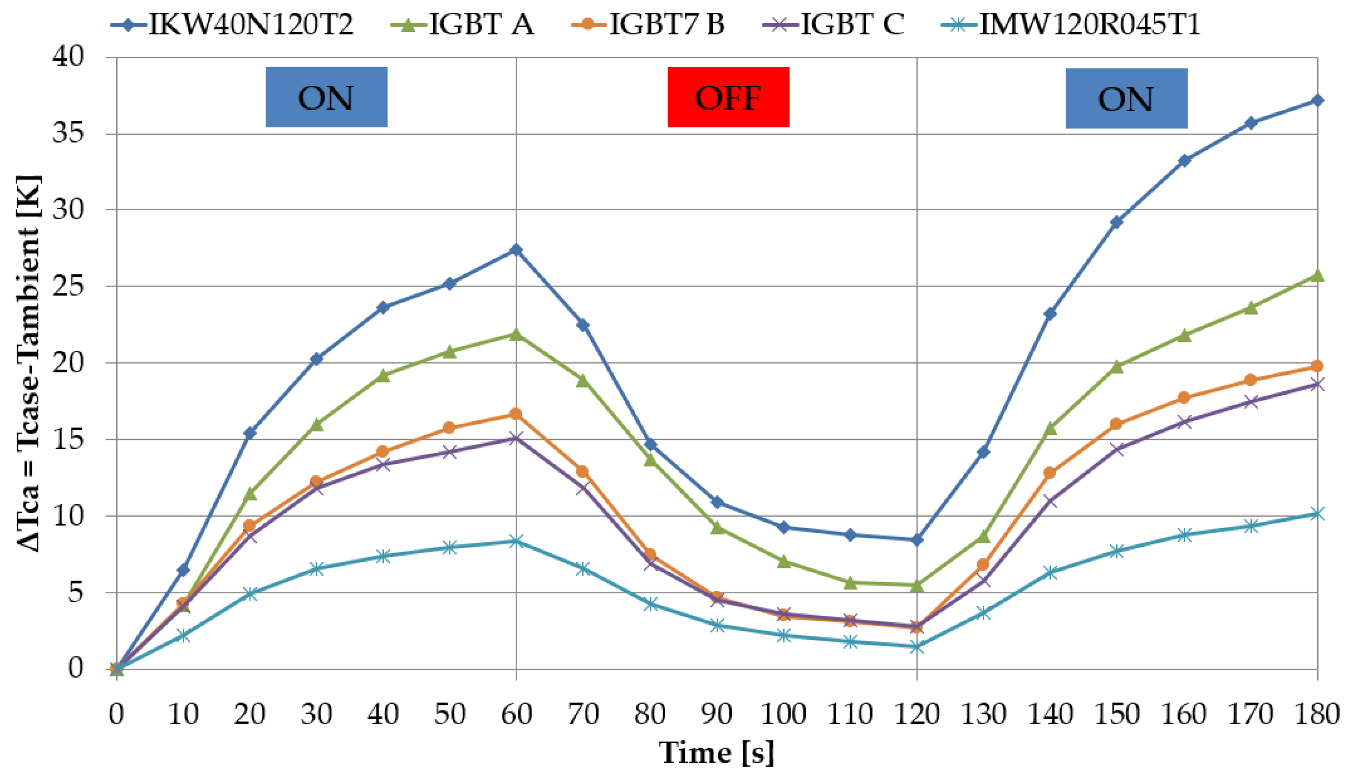
4.1. Inverter Power Semiconductor Selection

The power semiconductors of the three-phase inverter have been selected according to the voltage and current stresses. The voltage rating of the switches is a function of the DC-bus voltage VBUS and the overvoltage, as shown in (1).
V s w = V B L +   L ξ d i s w d t + V F R Δ V
In (1) VBL is the blocking voltage at steady state and ΔV is the switching overvoltage, function of different parameters such as the commutation inductance Lξ, the device current slope disw/dt and the forward recovery voltage VFR of the complementary freewheeling diode. In the three-phase inverter the blocking voltage VBL is equal to the DC-bus voltage VBUS. Thus, considering 700 V as a nominal DC-bus voltage VBUS the power semiconductors must withstand at least 700 V. However, the overvoltage ΔV must also be considered, especially in motor drive applications in which, as seen in the previous section, the overvoltage can be almost two times the DC-bus voltage VBUS in case of long power cable. Thus, SiC power MOSFETs with at least 1200 V blocking voltage must be chosen. To select the current rating of the power semiconductors, the average (AVG) and Root Means Square (RMS) currents flowing into switches have been calculated according to Equation (2).
I A V G = 1 T 0 0 T 0 [ i x ( t ) d s w ( t ) ] d t ,   I R M S = 1 T 0 0 T 0 [ i x 2 ( t ) d s w ( t ) ] d t
d x , t = 1 2 [ 1 + M 0 sin ( 2 π f 0 t ) ] ,   d x , b = 1 2 [ 1 M 0 sin ( 2 π f 0 t ) ] ,
{ I R M S , S x = 2 I O U T 1 24 π [ 8 M 0 cos φ 6 π D T f s w + 3 π ] I A V G , S x = 2 I O U T 2 [ 1 π 2 D T f s w π + M 0 cos φ 4 ] I R M S , D x = 2 I O U T 1 24 π [ 8 M 0 cos φ 6 π D T f s w + 3 π ] I A V G , D x = 2 I O U T 2 [ 1 π 2 D T f s w π M 0 cos φ 4 ]
In (2), T0 is the fundamental period, ix = I0sin(2πf0t2/3φ) is the phase current, with φ being the phase displacement, k = 0, 1, 2, x ∈ {A, B, C}, and dsw is the duty cycles of the switch. Using the Sinusoidal Pulse-Width-Modulation (S-PWM), the duty cycle of the top and bottom devices (dx,t and dx,b) can be derived from the Equation (3), where M0 is the modulation depth and f0 is the fundamental frequency. Substituting the (3) into (2), the RMS and AVG currents of the switch and diode can be written as in (4), where DT is the dead-time. According to this analysis the power semiconductors have been selected.

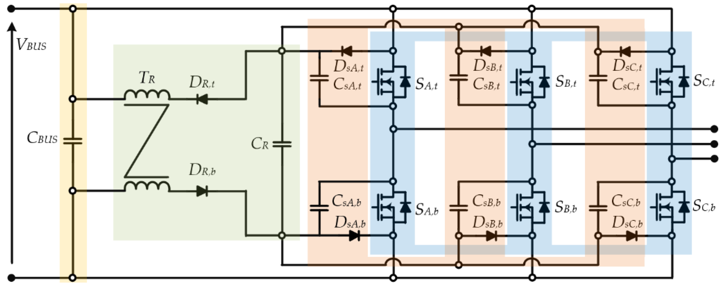
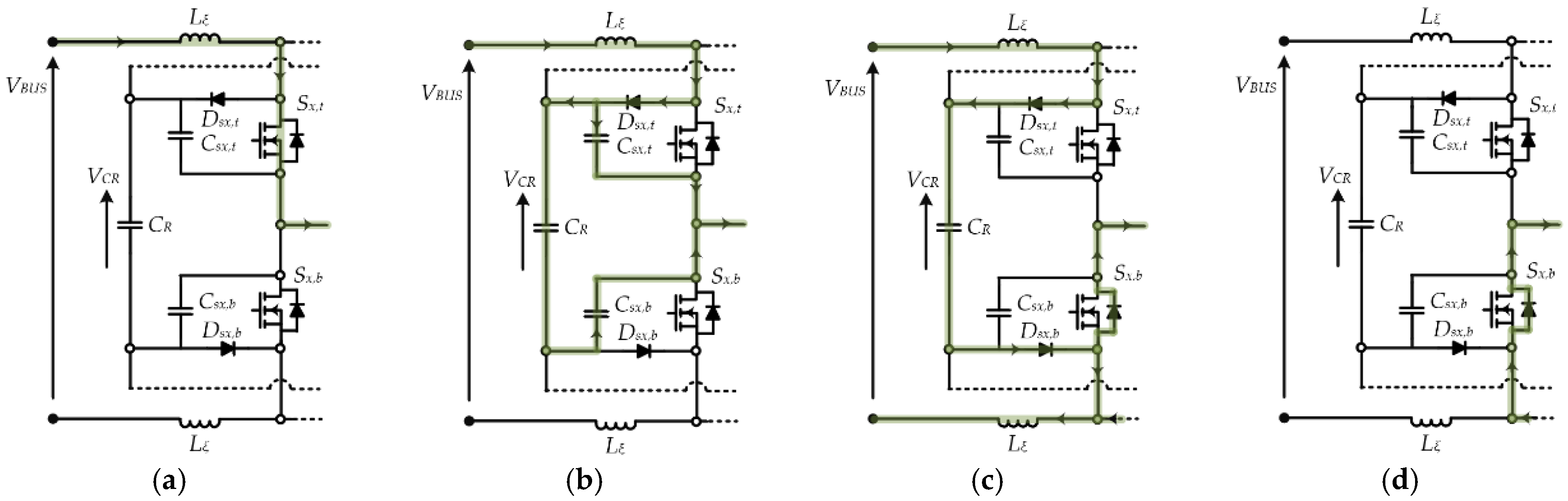
4.2. Snubber Circuit Design

The dV/dt is a function of the snubber capacitor values Csx,t and Csx,b, while the diodes Dsx,t and Dsx,b are used in order to block the current in one direction. During the turn-off of the switch Sx,t and turn-on of the switch Sx,b, the capacitor Csx,t is charged and the capacitor Csx,b is discharged; on the other hand, during the turn-on of the switch Sx,t and turn-off of the switch Sx,b the capacitor Csx,t is discharged and the capacitor Csx,b is charged. The recap of the turn-off of the switch Sx,t is illustrated in Figure 6, where the commutation inductance Lξ is clearly highlighted.
The turn-off of Sx,t occurs in four steps: after step 1, where the switch Sx,t is “on” and the current flows through it, the swich Sx,t is turned off, the snubber diode Dsx,t is “on” and the snubber capacitors Csx,t, Csx,b are respectively charged and discharged in step 2; in step 3, the snubber diode Dsx,b and the antiparallel diode Dx,b start to conduct the current; finally, in step 4, the current flows through the diode Dx,b and the switch Sx,b will be turned on under zero voltage. The turn-off of the bottom swich Sx,b will occur in a similar way. In state two the commutation inductance Lξ and snubber capacitor Csx,t form a resonant circuit, thus the second-order differential equation can be written in (5). The solution of the (5) is given in (6), where ωr = 1/ L ξ   C s x , t   is the resonant frequency, Zr = L ξ   / C s x , t   is the damping factor, VCsx,t,0 is the initial voltage of the capacitor Csx,t and IL0 is the initial current of the commutation inductance Lξ. From the Equation (6), the dV/dt across the power switch can be obtained as in (7).
d V C s x , t 2 d t + V C s x , t L ξ C s x , t = V B U S L ξ C s x , t
V C s x , t = V B U S ( V B U S V C s x , t , 0 ) cos ( ω r t ) + Z r I L , 0 sin ( ω r t )
d V C s x , t d t = ω r ( V B U S V C s x , t , 0 ) sin ( ω r t ) + ω r Z r I L , 0 cos ( ω r t )
It can be seen from (7) that the overvoltage is a function of the commutation inductance Lξ, the snubber capacitance Csx,t and the initial current value IL0. On one hand, high value of the inductance Lξ provides low value of the resonant frequency ωr and high value of the damping factor Zr; consequently, the overvoltage will be high. The high initial current value also provides high overvoltage. On the other hand, the high value of the snubber capacitance Csx,t results in low resonant frequency ωr and damping factor Zr values; consequently the overvoltage during the commutation will be low. Finally, from (7) di/dt can be written as in (8). It can be noticed that di/dt is strictly dependent on the inductance Lξ and the initial current value IL0.
d i d t = 1 L ξ ( V B U S V C s x , t , 0 ) sin ( ω r t ) ω r I L , 0 cos ( ω r t )
The maximum value of dV/dt and di/dt occurs when the load current is equal to zero, that is when ωrt = π/2, VCsx,t,0 = 0, IL,0 = 0, and they are equal to (9).
{ d V C s x , t d t = ω r V B U S d i d t = V B U S L ξ
From the obtained equations it is possible to select the snubber capacitors, considering that the commutation inductance Lξ depends on (1) the inductance Lσ introduced by the Printed Circuit Board (PCB) tracks that connect the switching devices to the DC-bus capacitor, (2) the inductance LESL related to the DC-bus capacitors and (3) the inductance LSW associated with the die and wire bond of the power semiconductors.

4.3. Recovery Energy Circuit Design

As it can be seen from Figure 5, the energy recovery circuit is created using two SiC diodes, the capacitor CR and the coupled inductor properly designed. The SiC diodes are used to have the unidirectional circulating current. The voltage stress of the diodes Dsx,t, Dsx,b, is equal to the DC-bus voltage VBUS plus the overvoltage, whereas the current stress is very low, since they are in on-state for a short time. The transferred average power as energy recovery is given in (10), where ΔIL,0 is the current ripple related to the DC-bus during each switching event.
P R = 3 ( 1 2 C s x , t + 1 2 C s x , b ) V B U S 2 f s w + f s w L ξ Δ I L , 0 2
According to the analysis presented in [39], using the S-PWM with 3rd harmonic injection and assuming three balanced loads, the DC-bus current ripple over the interval 0-π/3 is given in (11).
Δ I L , 0 2 = 3 π π 3 π 2 { 3 [ 2 I O U T sin ( ω 0 t φ ) ] 2 [ 2 I O U T sin ( ω 0 t 2 3 π ) ] 2 [ 2 I O U T sin ( ω 0 t 4 3 π ) ] 2 } d ω 0 t
Replacing (11) into (10) and performing some algebraic manipulations, the average power is given in (12).
P R = 3 ( 1 2 C s x , t + 1 2 C s x , b ) V B U S 2 f s w + f s w L ξ I O U T 2 2 [ 1 + 6 3 π ]
As it can be seen, the power managed by the energy recovery circuit is a function of switching frequency, load current, snubber capacitors and commutation inductance.

4.4. DC-bus Capacitor Design

The DC-bus capacitors are selected according to the DC-bus capacitor RMS current and DC-bus voltage ripple. It can be proven from [39] that the RMS current into DC-bus capacitor is given in (13).
I C r m s = I O U T M 0 [ 3 π + ( 4 3 π 9 4 M 0 ) cos 2 φ ]
This current is a function of the phase current IOUT, modulation depth M0, and phase displacement φ. Figure 7 shows the normalized RMS DC-bus current ICrms/IOUT as a function of the modulation depth M0 when cosφ = 1 and cosφ = 0.
As it can be seen, the maximum value of the RMS DC-bus current ICrms occurs when the cosφ is equal to 1 and the modulation depth M0 is between 0.55 and 0.6. The DC-bus capacitor must balance fluctuating instantaneous power on the DC-bus and its value can be selected according to the DC-bus voltage ripple. The required minimum DC-bus capacitor can be obtained from Equation (14), imposing the modulation depth M0 equal to 0.5.
C B U S , min = 3 ( 1 M 0 ) M 0 I O U T 2 f s w Δ V B U S

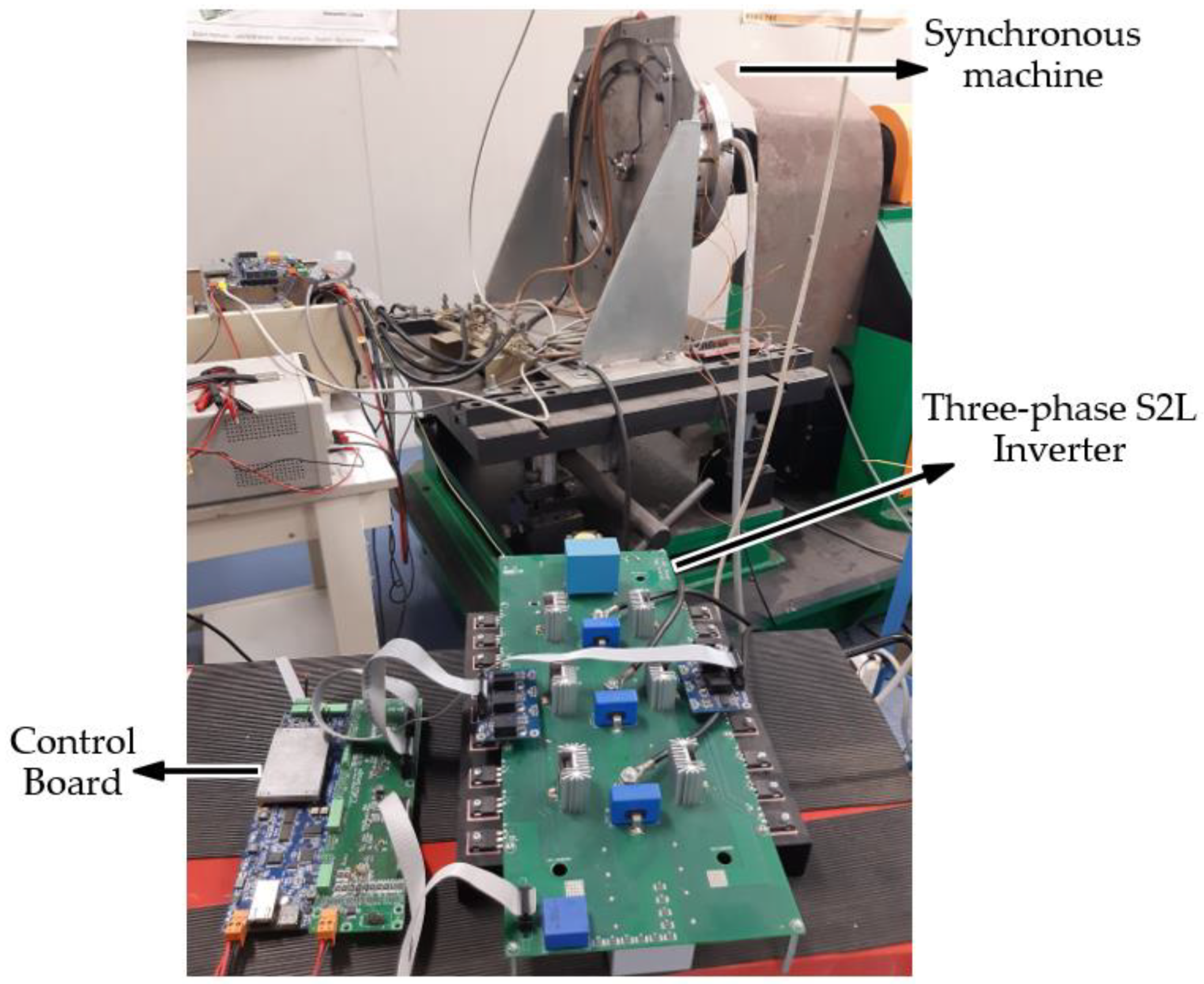
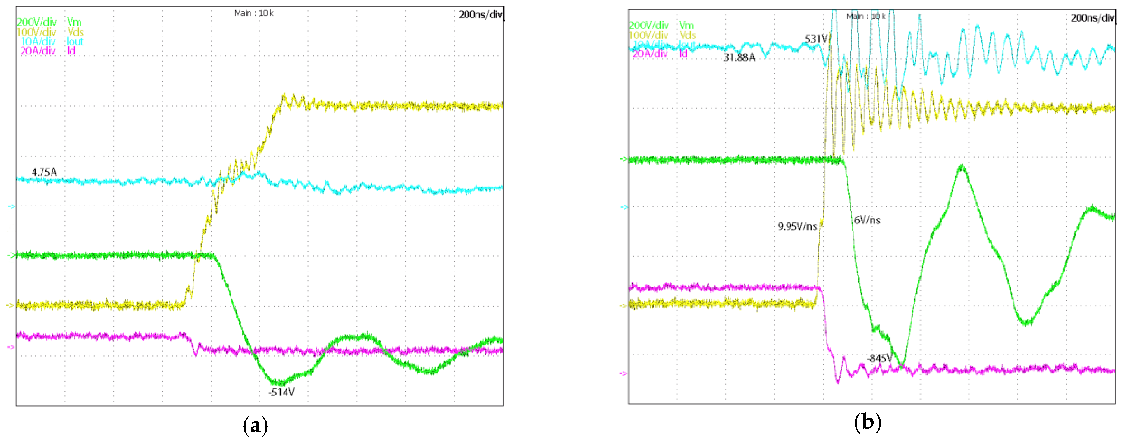
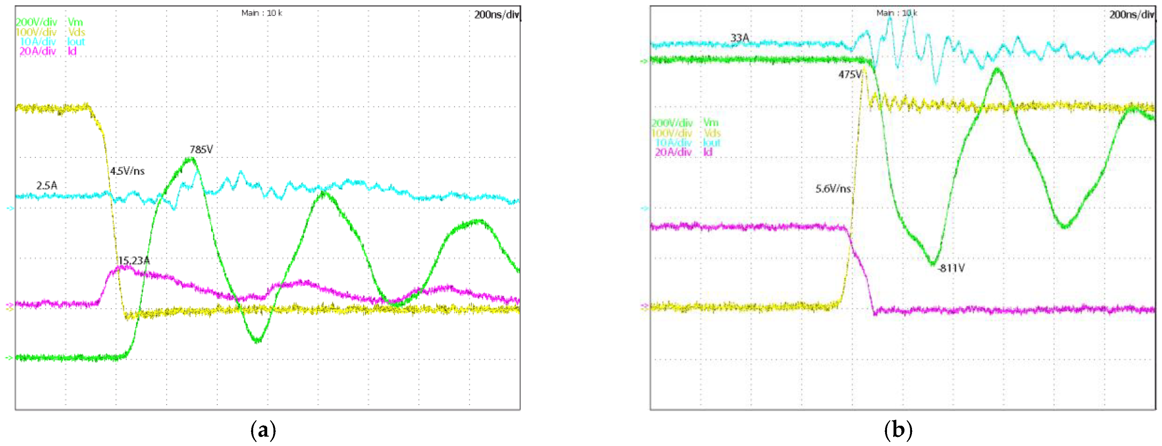
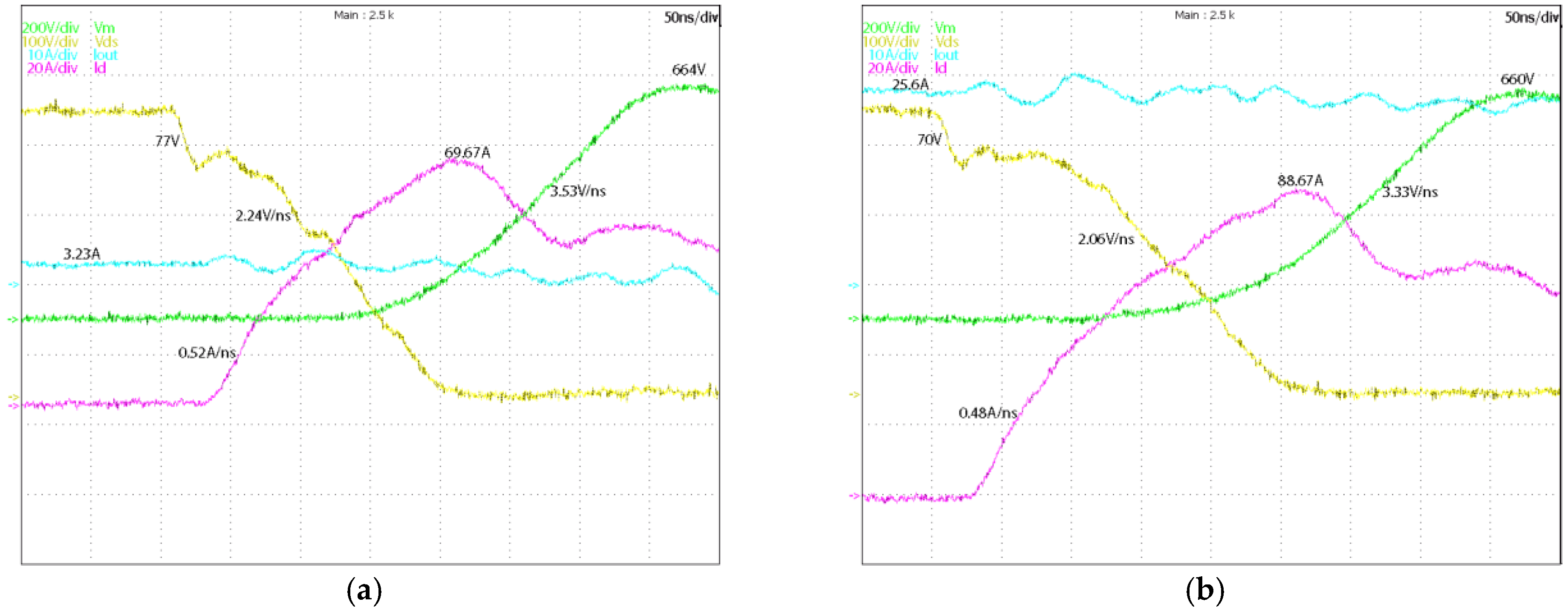
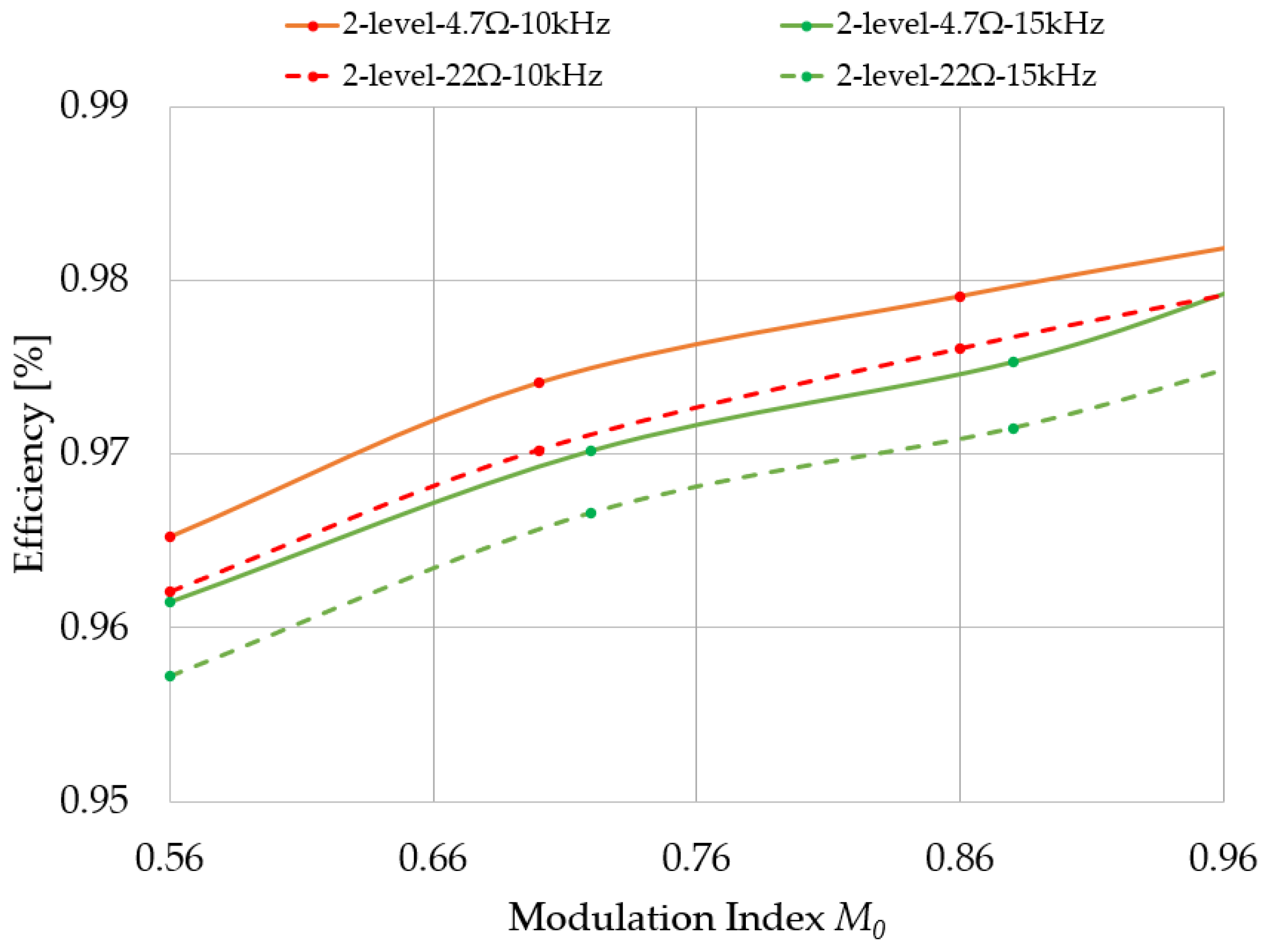
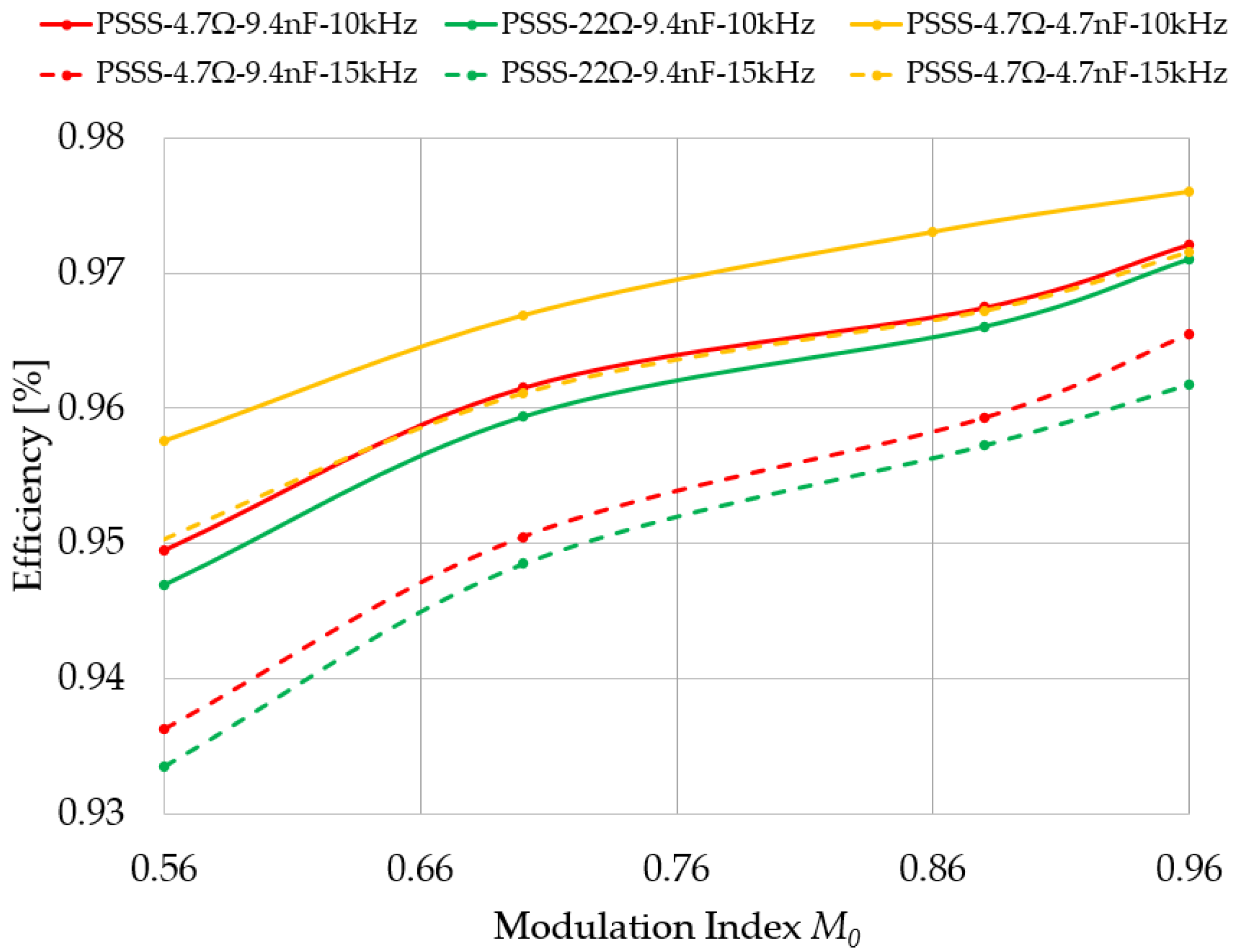
5. Experimental Results

According to the previous analysis, the three-phase S2L prototype converter has been realized. Particularly, given that the DC-bus is set at 700 V and the output power is set at 18 kW, 1700 V-45 mΩ SiC MOSFETs (part number C2M0045170D) and freewheeling parallel 1200 V-40 A SiC diodes (part number IDW40G120C5B) are selected. The snubber circuit is realized with one SiC diode and two Multilayer Ceramic Capacitors (MLCC). The chosen value of the snubber circuit capacitors CSx,t and CSx,b have been selected considering (7) and (8). The energy recovery circuit has been built using two SiC diodes (part number FFSD10120A) and a 40µF film capacitor (part number MKP1848). Based on (10), the coupled inductors have been designed in order to obtain 800 µH at the nominal load. The core selection has been based on the Area Product (AP) method. In particular, the number of turns is set at 41 and the material and the shape of the selected core are ferrite and EE 40/20, respectively. According to (13) and (14), four 40 µF film capacitors (part number MKP1848) are used as a DC-bus capacitor tank. All the components used to build up the S2L converter are listed in Table 2. To validate the proposed analysis and to obtain the overvoltage reduction at the motor side, using the SiC MOSFETs still keeping a high efficiency conversion, the experimental tests on the three-phase S2L inverter have been addressed. The experimental test setup is shown in Figure 8. It can be seen the three-phase S2L inverter, the synchronous machine, that is controlled by the S2L converter, mechanically coupled with an asynchronous machine can be controlled by an external test bench operating on 4-quadrants.
The S2L inverter and the electric drive are connected to each other by 15 m power cables (CF38.60.04 from Igus). The S2L inverter is controlled by a dedicated board based on the National Instruments sbRIO-9651 System on Module (SoM).
The DC-bus voltage VBUS is kept at 400 V using the DC Power Supply available in the laboratory. The achieved results from the three-phase S2L inverter have been compared to the three-phase 2L inverter with the same power devices. This latter inverter has been obtained by removing the snubber circuit and the energy recovery circuit form the three-phase S2L prototype converter. Thus, the power semiconductors and the parasitic inductor Lξ are completely the same in both converters. Figure 9 shows the turn-off of SA,t located in the three-phase 2L inverter when the gate resistance RG = 4.7Ω, the dead-time DT = 1 µs, the switching frequency fsw = 10 kHz and the power cable length lC = 15 m. When the phase current is equal to 4.75 A as in Figure 9a, the dV/dt in turn-on is really slow due to the total parasitic capacitances. The value of the voltage Vm at the motor side is only 1.285 times the VBUS. When the phase current increases from 4.75 A to 31.88 A the turn-off behavior is drastically changed, as illustrated in Figure 9b. Here, the commutation inductance shows the negative influences when the 2-level inverter is considered, since the dV/dt is fast (9.95 V/ns), and the voltage overshoot at the drain-source voltage is equal to 131 V (yellow track). This overshoot leads to a voltage at the motor terminals two times the VBUS (845 V). Figure 10 shows the turn-on and the turn-off of the SA,t located in the three-phase 2L inverter when the gate resistance RG = 22 Ω, dead-time DT = 1 μs, switching frequency fsw = 10 kHz and the power cable length lC = 15 m.
Increasing the gate resistance from 4.7 Ω to 22 Ω for both turn-on and turn-off, the overvoltage at the motor terminals is slightly reduced. As it can be seen from Figure 10a the phase current IA is equal to 2.5 A, the dV/dt is equal to 4.5 V/ns and the voltage at the motor side Vm is equal to 785 V. Figure 10b shows the turn-off when the phase current IA is equal to 33A. Thanks to the greater values of the RG both the dV/dt and the voltage overshoot at the device side are reduced to 5.6 V/ns and 75 V, respectively. However, the overvoltage Vm is still more than double of the VBUS (811 V is 2.02 times the VBUS). Figure 11 shows the turn-on of the SA,t located in the three-phase S2L inverter when the gate resistance RG = 4.7 Ω, snubber capacitors CSx,t = 9.4 μF, dead-time DT = 1 μs, switching frequency fsw = 10 kHz and the power cable length lC = 15 m. It is possible to notice that the overvoltage at the motor side is smaller than the previous case when the 2-level inverter is used. The values of the overvoltage at the motor terminal are 664 V and 660 V when the phase current IA is 3.23 A and IA is 25.6 A, respectively (almost 1.66 times the VBUS). The dV/dt is equal to 2.24 V/ns and 2.06 V/ns when the phase current is 3.23 A and 26.6 A, respectively.
It is possible to notice that the important parameter in the overvoltage issue is not the dV/dt but the rise time (fall time in turn-off) of the drain source voltage. If the two times of the travelling time (2td) of the voltage wave is greater than the rise/fall time (tf or tr) of the drain source voltage, a double voltage appears at the motor terminals.
Figure 12 shows the turn-off of SA,t located in the three-phase S2L inverter when the phase current is equal to 5.7 A and 31.42 A. It is possible to recognize two different dV/dt (yellow line): the first one related to the snubber capacitor dynamic is equal to 0.3 V/ns and the second one is related to the turn-on of the bottom switch. The voltage at the motor terminals Vm is only 52 V higher than the VBUS. When the phase current is 31.42 A (Figure 12b), the dV/dt is a little bit faster than the previous case (1.47 V/ns), but still no voltage overshoot occurs at the VDS and the overvoltage value is equal to 562 V (1.4 times the VBUS). The turn-off commutations of the three-phase S2L inverter occur at zero current; this means that all the losses are shifted to the turn-on commutations. The experimental efficiency of the three-phase 2L inverter and the three-phase S2L inverter is experimentally evaluated controlling the speed of the Permanent Magnet Synchronous Generators (PMSM) at constant torque. Figure 13 shows the efficiency of the three-phase 2L inverter versus modulations depth M0 for different values of the switching frequency (10 kHz and 15 kHz) and gate resistance (4.7 Ω and 22 Ω) when the power cable length lC is equal to 15 m, the DC-bus voltage VBUS is equal to 400 V and the phase peak current Ix is equal to 30 A.
The efficiency shows the increasing trend when the modulation depth M0 increases. However, when the gate drive resistance changes from 4.7 Ω to 22 Ω, the efficiency decreases. The efficiency trend at fsw = 10 kHz, RG = 22 Ω is close to the efficiency curve at fsw = 15 kHz, RG = 4.7 Ω. Figure 14 shows the efficiency of the three-phase S2L inverter versus modulations depth M0 for different values of the switching frequency (10 kHz and 15 kHz), gate resistance (4.7 Ω and 22 Ω) and snubber capacitors (4.7 nF and 9.4 nF) when the power cable length lC is equal to 15 m, the DC-bus voltage VBUS is equal to 400 V and the phase peak current Ix is equal to 30 A. As it can be seen, the efficiency of the three-phase S2L inverter is lower than the efficiency of the three-phase 2L inverter. This is due to the snubber circuit losses. Furthermore, the efficiency of the S2L inverter highly depends on the snubber capacitor values and the switching frequency. When a capacitor value of 4.7 nF is used, the drop of efficiency from switching frequency of 10 kHz to switching frequency of 15 kHz is less than 0.5% (orange line). On the other hand, when a 9.4 nF snubber value is used, the efficiency drop increase to 0.7%. This happens due to the high value of the inrush current into snubber capacitors during the turn on, which is a function of the snubber capacitor values. Higher value of snubber capacitor led to a higher inrush current. From the overvoltage mitigation point of view, the best S2L inverter setup happens when RG is equal to 4.7 Ω and the snubber capacitors CSx,t and Csx,b are equal to 9.4 nF. In this condition, the performance of the S2L inverter is slightly lower than the 2L inverter.

6. Conclusions

The benefits of using SiC MOSFETs in the motor drive applications have been discussed in the first part of this paper. The experimental tests performed on the power semiconductors in the first part of the paper show that SiC MOSFET (IMW120R045T1) allows a huge improvement in terms of temperature performance compared to the IGBTs. After that, the overvoltage issue when the electric drive is supplied by the converter with long power cables has been highlighted and supported by the experimental tests. The latter illustrate that the voltage at the motor terminal Vm is two times the DC bus voltage VBUS when the length of the power cable is equal to 15 m or 30 m. A case study of a three-phase two level inverter with the addition of snubber circuits has been discussed to solve the overvoltage problem in the motor drive application. Particularly, the prototype of the S2L inverter has been built according to the proposed design guidelines. Experimental results confirm the effectiveness of the proposed converters in significantly reducing the overvoltage at motor terminals and mitigating the windings insulation stress. When the 2L inverter is used the peak voltage at the motor side is equal to 845 V and the dV/dt is equal to 9.95 V/ns, while in the S2L inverter the peak voltage is equal to 562 V and the dV/dt is equal to 1.47 V/ns. However, the conversion efficiency is slightly reduced compared to the three-phase 2L inverter. Considering the same operating conditions, the peak efficiency of the three-phase 2L inverter is equal to 0.982%, whereas the peak efficiency of the three-phase S2L inverter is equal to 0.976%. Consequently, the proposed analysis shows that by using the S2L inverter it is possible to find a good compromise between dV/dt, overvoltage and efficiency performance of the entire electric drive system.

Author Contributions

Conceptualization, L.S. and A.L.; methodology, L.S. and A.L.; software, M.d.B. and L.B.; validation, M.d.B. and L.B.; formal analysis, M.d.B. and L.B.; investigation, M.d.B.; resources, L.B. and M.d.B.; data curation, M.d.B. and L.B.; writing—original draft preparation, M.d.B. and L.B.; writing— review and editing L.S., and A.L.; visualization, M.d.B.; supervision, L.S. and A.L.; project administration, L.S. and A.L.; funding acquisition, L.S. All authors have read and agreed to the published version of the manuscript.

Funding

This research was funded by “ECPE—European Center for Power Electronics”.

Institutional Review Board Statement

The study does not involve humans or animals.

Informed Consent Statement

The study does not involve humans or animals.

Data Availability Statement

The study does not report any data.

Conflicts of Interest

The authors declare no conflict of interest.

References

  1. Jafari, A.; Nikoo, M.S.; Perera, N.; Yildirim, H.K.; Karakaya, F.; Soleimanzadeh, R.; Matioli, E. Comparison of Wide-Band-Gap Technologies for Soft-Switching Losses at High Frequencies. IEEE Trans. Power Electron. 2020, 35, 12595–12600. [Google Scholar] [CrossRef]
  2. Shenai, K. High-Density Power Conversion and Wide-Bandgap Semiconductor Power Electronics Switching Devices. Proc. IEEE 2019, 107, 2308–2326. [Google Scholar] [CrossRef]
  3. Tong, Z.; Gu, L.; Ye, Z.; Surakitbovorn, K.; Rivas-Davila, J. On the Techniques to Utilize SiC Power Devices in High- and Very High-Frequency Power Converters. IEEE Trans. Power Electron. 2019, 34, 12181–12192. [Google Scholar] [CrossRef]
  4. La Mendola, M.; Di Benedetto, M.; Lidozzi, A.; Solero, L.; Bifaretti, S. Four-Port Bidirectional Dual Active Bridge Converter for EVs Fast Charging. In Proceedings of the 2019 IEEE Energy Conversion Congress and Exposition (ECCE), Baltimore, MD, USA, 29 September–3 Octomber 2019; pp. 1341–1347. [Google Scholar]
  5. Hussain, M.W.; Elahipanah, H.; Zumbro, J.E.; Rodriguez, S.; Malm, B.G.; Mantooth, H.A.; Rusu, A. A SiC BJT-Based Negative Resistance Oscillator for High-Temperature Applications. IEEE J. Electron Devices Soc. 2019, 7, 191–195. [Google Scholar] [CrossRef]
  6. Funaki, T.; Balda, J.C.; Junghans, J.; Kashyap, A.S.; Mantooth, H.A.; Barlow, F.; Hikihara, T. Power Conversion With SiC Devices at Extremely High Ambient Temperatures. IEEE Trans. Power Electron. 2007, 22, 1321–1329. [Google Scholar] [CrossRef]
  7. Anderson, J.A.; Hanak, E.J.; Schrittwieser, L.; Guacci, M.; Kolar, J.W.; Deboy, G. All-Silicon 99.35% Efficient Three-Phase Seven-Level Hybrid Neutral Point Clamped/Flying Capacitor Inverter. Cpss Trans. Power Electron. Appl. 2019, 4, 50–61. [Google Scholar] [CrossRef]
  8. Di Benedetto, M.; Solero, L.; Crescimbini, F.; Lidozzi, A.; Grbovic, P.J. 5-Level E-type back to back Power Converters—A New Solution for Extreme Efficiency and Power Density. In Proceedings of the 2017 13th Conference on Ph.D. Research in Microelectronics and Electronics (PRIME), Giardini Naxos, Italy, 12–15 June 2017; pp. 341–344. [Google Scholar]
  9. Di Benedetto, M.; Lidozzi, A.; Solero, L.; Crescimbini, F.; Grbovic, P.J. Five-Level back to back E-Type Converter for High Speed Gen-Set Applications. In Proceedings of the IECON 2016—42nd Annual Conference of the IEEE Industrial Electronics Society, IEEE, Florence, Italy, 24–27 October 2016; pp. 3409–3414. [Google Scholar]
  10. Di Benedetto, M.; Lidozzi, A.; Solero, L.; Grbovic, P.J.; Bifaretti, S. ISOP DC-DC Converters Equipped 5-Level Unidirection-al T-Rectifier for Aerospace Applications. In Proceedings of the 2015 IEEE Energy Conversion Congress and Exposition (ECCE), Montreal, QC, Canada, 20–24 September 2015; pp. 1694–1700. [Google Scholar]
  11. Di Benedetto, M.; Lidozzi, A.; Solero, L.; Crescimbini, F.; Grbovic, P.J. Low-Frequency State-Space Model for the Five-Level Unidirectional T-Rectifier. IEEE Trans. Ind. Appl. 2017, 53, 1127–1137. [Google Scholar] [CrossRef]
  12. Di Benedetto, M.; Lidozzi, A.; Solero, L.; Crescimbini, F.; Grbovic, P.J. Small-Signal Model of the Five-Level Unidirec-tional T-Rectifier. IEEE Trans. Power Electron. 2017, 32, 5741–5751. [Google Scholar] [CrossRef]
  13. Klobucar, B.; Yuan, Z. 1200V Discrete CoolSiC(TM) MOSFETs in a Comparison with the Trenchstop HighSpeed IGBTs for High-Speed Spindles and Servo Drive System. In Proceedings of the PCIM Europe digital days 2020; International Exhibition and Conference for Power Electronics, Intelligent Motion, Renewable Energy and Energy Management, Nuremberg, Germany, 7–8 July 2020; pp. 1–6. [Google Scholar]
  14. Han, D.; Sarlioglu, B. Comprehensive Study of the Performance of SiC MOSFET-Based Automotive DC–DC Converter under the Influence of Parasitic Inductance. IEEE Trans. Ind. Appl. 2016, 52, 5100–5111. [Google Scholar] [CrossRef]
  15. Yang, Y.; Wen, Y.; Gao, Y. A Novel Active Gate Driver for Improving Switching Performance of High-Power SiC MOSFET Modules. IEEE Trans. Power Electron. 2019, 34, 7775–7787. [Google Scholar] [CrossRef]
  16. Morya, A.K.; Gardner, M.C.; Anvari, B.; Liu, L.; Yepes, A.G.; Doval-Gandoy, J.; Toliyat, H.A. Wide Bandgap Devices in AC Electric Drives: Opportunities and Challenges. IEEE Trans. Transp. Electrif. 2019, 5, 3–20. [Google Scholar] [CrossRef]
  17. Narayanasamy, B.; Sathyanarayanan, A.S.; Luo, F.; Chen, C. Reflected Wave Phenomenon in SiC Motor Drives: Conse-quences, Boundaries, and Mitigation. IEEE Trans. Power Electron. 2020, 35, 10629–10642. [Google Scholar] [CrossRef]
  18. Leuzzi, R.; Monopoli, V.G.; Cupertino, F.; Zanchetta, P. Comparison of Two Possible Solution for Reducing Over-voltages at the Motor Terminals in High-Speed AC Drives. In Proceedings of the 2019 21st European Conference on Power Electronics and Applications (EPE ’19 ECCE Europe), Genova, Italy, 3–5 Septemper 2019; pp. P.1–P.10. [Google Scholar]
  19. Rodríguez, J.; Pontt, J.; Silva, C.; Musalem, R.; Newman, P.; Vargas, R.; Fuentes, S. Resonances and overvoltages in a medium-voltage fan motor drive with long cables in an under-ground mine. IEEE Trans. Ind. Appl. 2006, 42, 856–863. [Google Scholar] [CrossRef]
  20. Skibinski, G.; Leggate, D.; Kerkman, R. Cable Characteristics and Their Influence on Motor over-Voltages. In Proceedings of the APEC 97—Applied Power Electronics Conference, Atlanta, GA, USA, 27 February 1997; Volume 1, pp. 114–121. [Google Scholar]
  21. Persson, E. Transient effects in application of PWM inverters to induction motors. IEEE Trans. Ind. Appl. 2002, 28, 1095–1101. [Google Scholar] [CrossRef]
  22. Pulsinelli, F.; Solero, L.; Chiola, D.; Sobe, K.; Brucchi, F. Overvoltages at Motor Terminals in SiC Electric Drives. In Proceedings of the 2018 International Symposium on Power Electronics, Electrical Drives, Automation and Motion (SPEEDAM), Amalfi, Italy, 20–22 June 2018; pp. 513–518. [Google Scholar]
  23. Kerkman, R.J.; Leggate, D.; Schlegel, D.; Skibinski, G. PWM Inverters and Their Influence on Motor Overvoltage. In Proceedings of the APEC—Applied Power Electronics Conference, Atlanta, GA, USA, 27 February 1997; Volume 1, pp. 103–113. [Google Scholar]
  24. Amarir, S.; Al-Haddad, K. Mathematical Analysis and Experimental Validation of Transient over-Voltage Higher than 2 per Unit along Industrial ASDM Long Cables. In Proceedings of the 2008 IEEE Power Electronics Specialists Conference, Rhodes, Greece, 15–19 June 2008; pp. 1846–1851. [Google Scholar]
  25. Zhao, F.; Xiao, G.; Zhu, T.; Zhao, T.; Zheng, X.; Wu, Z. Harmonic Analysis and Suppression Method of Output Current Distortion for Medium-Voltage Motor Drives with Modular Multilevel Converter. IEEE Trans. Power Electron. 2019, 35, 744–759. [Google Scholar] [CrossRef]
  26. Akagi, H.; Doumoto, T. An Approach to Eliminating High-Frequency Shaft Voltage and Ground Leakage Current from an Inverter-Driven Motor. IEEE Trans. Ind. Appl. 2004, 40, 1162–1169. [Google Scholar] [CrossRef]
  27. Zhou, W.; Diab, M.S.; Yuan, X. Mitigation of Motor Overvoltage in SiC-Device-Based Drives using a Soft-Switching In-verter. In Proceedings of the 2020 IEEE Energy Conversion Congress and Exposition (ECCE), Detroit, MI, USA, 11–15 October 2020; pp. 662–669. [Google Scholar]
  28. Yuen, K.K.-F.; Chung, H.S.-H.; Cheung, V.S.-P. An Active Low-Loss Motor Terminal Filter for Overvoltage Suppression and Common-Mode Current Reduction. IEEE Trans. Power Electron. 2011, 27, 3158–3172. [Google Scholar] [CrossRef]
  29. Parreiras, T.M.; Prado, B.M.P.D.; Filho, B.D.C. Common-Mode Overvoltage Mitigation in a Medi-um-Voltage Pump Motor Transformerless Drive in a Mining Plant. IEEE Trans. Ind. Appl. 2018, 54, 848–857. [Google Scholar] [CrossRef]
  30. Peng, F.; Su, G.-J.; Tolbert, L. A passive soft-switching snubber for PWM inverters. IEEE Trans. Power Electron. 2003, 19, 363–370. [Google Scholar] [CrossRef]
  31. Pulsinelli, F.; Di Benedetto, M.; Lidozzi, A.; Solero, L.; Crescimbini, F. Power Losses Distribution in SiC Inverter Based Electric Motor Drives. IEEE Trans. Ind. Appl. 2019, 55, 7843–7853. [Google Scholar] [CrossRef]
  32. Akagi, H.; Matsumura, I. Overvoltage Mitigation of Inverter-Driven Motors with Long Cables of Different Lengths. IEEE Trans. Ind. Appl. 2011, 47, 1741–1748. [Google Scholar] [CrossRef]
  33. De Caro, S.; Foti, S.; Scimone, T.; Testa, A.; Scelba, G.; Pulvirenti, M.; Russo, S. Motor Overvoltage Mitigation on SiC MOSFET Drives Exploiting an Open-End Winding Configuration. IEEE Trans. Power Electron. 2019, 34, 11128–11138. [Google Scholar] [CrossRef]
  34. Zhang, Y.; Li, H.; Peng, F.Z. A Low-Loss Compact Reflected Wave Canceller for SiC Motor Drives. IEEE Trans. Power Electron. 2021, 36, 2461–2465. [Google Scholar] [CrossRef]
  35. Parida, N.; Das, A. A Modular Multilevel Converter with Filter Capacitor for Long-Cable-Fed Drive Application. IEEE Trans. Ind. Appl. 2019, 55, 7833–7842. [Google Scholar] [CrossRef]
  36. Cai, M.; Wasynczuk, O.; Saeedifard, M. A Voltage-Edge-Rate-Limiting Soft-Switching Inverter Based on Auxiliary Reso-nant Pole. IEEE J. Emerg. Sel. Top. Power Electron. 2019, 7, 736–744. [Google Scholar] [CrossRef]
  37. Bellomo, J.P.; Lebey, T.; Oraison, J.M.; Peltier, F. Influence of Rise Time on the Dielectric Behavior of Stator Insulation Mate-rials. In Proceedings of the Conference on Electrical Insulation and Dielectric Phenom—CEIDP ’96, Millbrae, CA, USA, 23 October 1996; Volume 2, pp. 842–845. [Google Scholar]
  38. Fabiani, D.; Montanari, G.C.; Cavallini, A.; Mazzanti, G. Relation between space charge accumulation and partial dis-charge activity in enameled wires under PWM-like voltage waveforms. IEEE Trans. Dielectr. Electr. Insul. 2004, 11, 393–405. [Google Scholar] [CrossRef]
  39. Pei, X.; Zhou, W.; Kang, Y. Analysis and Calculation of DC-Link Current and Voltage Ripples for Three-Phase Inverter With Unbalanced Load. IEEE Trans. Power Electron. 2015, 30, 5401–5412. [Google Scholar] [CrossRef]
Figure 1. Experimental setup used for testing the effect of the long power cable connected to the motor on the power semiconductors.
Energies 14 01690 g001
Figure 2. Thermal behavior of the power semiconductors in motor drive application.
Energies 14 01690 g002
Figure 3. Voltage waveform across the inverter and the motor during the turn-off.
Energies 14 01690 g003
Figure 4. Voltage waveform across the inverter and the motor during the turn-on.
Energies 14 01690 g004
Figure 5. Electrical circuit of snubber two-level (S2L) inverter: (1) DC-bus capacitor in orange, (2) recovery circuit in green, (3) three-phase inverter circuit in blue, and (4) snubber circuit in pink.
Energies 14 01690 g005
Figure 6. Current path highlighted in green during the turn-off of Sx,t: (a) step 1, (b) step 2, (c) step 3, (d) step 4.
Energies 14 01690 g006
Figure 7. Normalized RMS DC-bus current as a function of the modulation depth: (a) cosφ = 1, (b) cosφ = 0.
Energies 14 01690 g007
Figure 8. Experimental setup with S2L prototype including the motor drive.
Energies 14 01690 g008
Figure 9. Turn-off of SA,t located in the three-phase 2L inverter with RG = 4.7 Ω, dead-time DT = 1 µs, switching frequency fsw = 10 kHz and lC = 15 m: (a) phase current of 4.75 A, (b) phase current of 31.88 A. Line-to-line voltage Vm at the motor side (green track), drain-source voltage VDS of the SA,t (yellow track), drain current of SA,t (magenta track) and phase current IA (ciano track).
Energies 14 01690 g009
Figure 10. Commutation of SA,t located in the three-phase 2L inverter with RG = 22 Ω, dead-time DT = 1 µs, switching frequency fsw = 10 kHz and lC = 15 m: (a) turn-off, (b) turn-on. Line-to-line voltage Vm at the motor side (green track), drain-source voltage VDS of the SA,t (yellow track), drain current of SA,t (magenta track) and phase current IA (ciano track).
Energies 14 01690 g010
Figure 11. Turn-on of SA,t located in the three-phase S2L inverter with RG = 4.7Ω, CSA,t = 9.4 μF dead-time DT = 1 μs, switching frequency fsw = 10 kHz and lC = 15 m: (a) phase current of 3.23 A, (b) phase current of 25.6 A. Line-to-line voltage Vm at the motor side (green track), drain-source voltage VDS of the SA,t (yellow track), drain current of SA,t (magenta track) and phase current IA (ciano track).
Energies 14 01690 g011
Figure 12. Turn-off of SA,t located in the three-phase S2L inverter with RG = 4.7Ω, CSA,t = 9.4 µF dead-time DT = 1 µs, switching frequency fsw = 10 kHz and lC = 15 m: (a) phase current of 5.7 A, (b) phase current of 25.6 A. Line-to-line voltage Vm at the motor side (green track), drain-source voltage VDS of the SA,t (yellow track), drain current of SA,t (magenta track) and phase current IA (ciano track).
Energies 14 01690 g012
Figure 13. Efficiency of the three-phase 2L inverter as a function of modulation depth M0 with lC = 15 m VBUS = 400 V, Ix = 30 A.
Energies 14 01690 g013
Figure 14. Efficiency of the three-phase S2L inverter as a function of modulation depth M0 with lC = 15 m VBUS = 400 V, Ix = 30 A.
Energies 14 01690 g014
Table 1. Operating parameters of each power semiconductors used as DUT.
Part NumberIKW40N120T2IGBT AIGBT BIGBT CIMW120R045T1
PackageTO 247-3TO 247-3TO 247-3TO 247-3TO 247-3
TechnologySiSiSiSiSiC
RGon [Ω]2047201033.2
RGoff [Ω]2148211133.2
VGE or VGS on [V]1212151520
VGE or VGS off [V]−15−15−5−5−5
VBUS [V]330330330330520
IPhase RMS [A]14.114.112.612.614.4
Modulation depth M0110.950.950.95
fsw [kHz]1010101010
f0 [Hz]5050505050
Dead-Time [µs]1.81.8111
Table 2. Component description used to build the three-phase S2L prototype.
ReferencePart NumberDescription
Sx,t, Sx,bC2M0045170DC2M0045170D: Cree SiC MOSFET 1700V-45mΩ-TO247-3
Dx,t, Dx,bIDW40G120C5BIDW40G120C5B: Infineon SiC Diode 1200V-40A-TO247-3
DSx,t, DSx,bIDW40G120C5BInfineon SiC Diode 1200V-40A-TO247-3
CSx,t, CSx,b1812SC472KAT1AAVX MLC Capacitor 4.7nF-1500V
DR,t,-DR,bFFSD10120AOn Semiconductor SiC Diode 1200V-10A-DPAK
CRMKP1848MKP1848: Vishay Film Capacitor 40µF 900V
TRN.A.ICE Mutual Inductor 1:1-800µH-4A-E42/20 Ferrite
CBUS5xMKP1848Vishay Film Capacitor 40 µF 900 V
Current SensorLA100-TPLEM Current Transducer IPN = 100 A
Voltage SensorLV 20-PLEM Voltage Transducer
HeatsinkSK 56/100 SAFischer Elektronik 300 mm × 100 mm × 40 mm
Publisher’s Note: MDPI stays neutral with regard to jurisdictional claims in published maps and institutional affiliations.

