Article

Design, Analysis and Implementation of the Tapped-Inductor Boost Current Converter on Current Based System

Department of Electrical Engineering, The Hong Kong Polytechnic University, Kowloon, Hong Kong 8523, China
*
Author to whom correspondence should be addressed.
Energies 2021, 14(4), 888; https://doi.org/10.3390/en14040888
Submission received: 6 August 2020 / Revised: 21 January 2021 / Accepted: 26 January 2021 / Published: 8 February 2021
(This article belongs to the Special Issue Energy Management in the Multi-Source Systems)

Abstract

:
Power converters play a crucial role in renewable energy systems. Most well-known power conversion topologies are voltage mode, not current mode. Current mode converters are more appropriate for renewable energy systems such as photovoltaic systems since solar panels are typical current sources. The vast usage of battery as energy storage is also a current sink for constant current mode charging. Utilizing current mode converters should be more straightforward and judicious. In this study, a new topology for the tapped-inductor power conversion circuit family is introduced. The proposed topology has been investigated thoroughly based on theories, simulations and experiments. The boost version is examined as an example to downstate the performance. A detailed comparison with the conventional boost current converter is conducted in this paper.

1. Introduction

Fossil fuels are going to be exhausted. Seeking other energy resources should be unavoidable. Sustainable energy resources should be the most desirable resources for us. Renewable energy resources are the good choices for us. Wind and Solar Energy resources are the most popular resources [1,2,3,4]. Some countries have planned to use the renewable energy resources to replace the fossil fuels [5,6,7,8,9,10]. Boost converters act a major role in the renewable energy systems [11,12,13,14,15,16]. It can raise the input voltage to meet the output needs since the renewable energy resources such as photovoltaic panels provide low voltage normally from 12 V to 24 V. Hence, a high efficiency, high gain and simple construction boost converter topologies have been demanded. Tapped-inductor boost converter is one of the topologies which has high voltage gain, high efficiency and simple structure [17,18]. However, most of researchers have been working on the voltage mode, rather than current mode. Current mode boost converters are in fact very useful. Some renewable energy resources and loads are typical current sources not voltage sources. For instance, photovoltaic panel is a typical current source. Using current mode converter to convert the current source is the most directly and efficiently. The current mode converter also can act as a motor torque controlled driver since the motor torque can be changed by the armature current in proportion. Furthermore, the current mode converter can be used to form an LED driver since the brightness of the LED is altered in proportional to the input current. Except for the Tapped-inductor boost converter topology, many different types of the boost converters topologies have been explored for researchers in recent years such as Switched capacitor, Switched inductor and Cascaded. All these topologies have their pros and cons. Also, different topologies have their proper applications.

1.1. Switched Capacitor

Switched Capacitor is one of the typical techniques for boosting voltage [19,20]. The voltage level can be stepped up by capacitive energy transfer solely and the magnetic energy transfer is not involved. Switched capacitor topologies are very prevalent since their configurations have high flexibility and variability. There are many switched capacitor topologies have been explored and investigated such as Doubler, Series- parallel and Ladder. For Doubler switched capacitor topology [21], the output voltage is doubled with the input voltage in all stages. For the Series- parallel switched-capacitor topology [22,23,24], each capacitor is charged up the same voltage. The output voltage can be boosted by connecting the charged capacitors together with the input voltage. The output voltage is boosted in higher voltage level when the number of the capacitors connected in series is increased. For the Ladder switched capacitor topology [25,26], it combine with two groups of capacitors. This topology can attain different voltage gains. The switched capacitor boost converters have a lots of advantage, they boost the output voltage by capacitive energy, not inductive energy. Hence, this type of converters can be compacted in size and of lightweight. Also, most of the switched capacitor topologies have high flexibility and variability. It can reach wide range of voltage gain by different number of the capacitors to be combined together. However, the Switched capacitor topologies have high transient current. This increases the switches current stress and sophisticated components should be affected. Switched capacitor boost converter is used for the high voltage applications.

1.2. Switched Inductor

Active switched inductor boost converter consists of two active switches in the active switched inductor module. There is not necessary equipped with external switch in the converter circuit. The improved active switched inductor boost converter can acquire high voltage gain by adding a pair of diodes and capacitors in the circuit [27]. It also can reduce the voltage stress on the switches. In literature [28], Quasi active switched inductor with coupled inductors was introduced. The advantages for adding coupled inductor are that it can obtain high voltage gain with less stress to the switches. Moreover, the voltage gain can be altered by the turns ratio of the coupled inductors. Switched inductor boost converters can be used as Mid-range DC/DC converters. They are not suitable for the high power applications.

1.3. Cascaded

Another technique which is popular for use to boost the voltage is cascading. The main idea for this type of the boost converter is required to connect two or more units of boost converters in cascaded [29,30]. Quadratic boost converter is a classic example for the cascaded boost converter which is formed by two boost converters in the cascaded [31,32,33]. The first step converter with the voltage stress is lower when compared with the second step of the converter. Hence, the first step converter is conducted relatively longer period. On the other hand, the duty ratio of the second phase converter is less in order to reduce the switching loss. The quadratic boost converter can provide a wide range of voltage gain. However, the duty cycle only can change slightly. The quadratic boost converter also can combine another type boost converter to form a Hybrid cascaded boost converter such as combining the quadratic boost converter with voltage multiplier [34,35]. This can boost the voltage gain of the converter to be sufficient for the high voltage applications. The major advantage of this type converter is that it can achieve high voltage gain and be capable for high power performance. Thus, this converter type is appropriate to HVDC transmission. But, this kind of converters is comparatively expensive and heavy since their structures are complex and consist of a lot of components.

1.4. Tapped Inductor

Tapped-inductor boost converter can be divided into three different groups including switched-tapped, diode-tapped and rail-tapped. Their constructions are similar, using the same number and type of the components except for the tapping and connections of the components are different. The major advantage of this kind of converters is that the output voltage is mainly adjusted by the turns ratio of the tapped-inductor, not solely depends on the duty cycle. Hence, the switching loss can be reduced. Also, the output voltage range can be wider. Many tapped-inductor topologies have been explored. However, researchers have been sticked on the voltage mode studies, not current mode [36,37]. In paper [38], the double tapped-inductor boost converter was introduced. This topology improved the basic tapped-inductor voltage conversion ratio. It can reduce the turns ratio of the tapped-inductor but the voltage boosting capability can remain unchanged. Tapped-inductor boost converter is suitable for the Photovoltaic systems. This kind of converters has features of high variability and wide output range [39,40]. The new proposed tapped-inductor boost converter has high current conversion ratio and efficiency. It is more appropriate for Photovoltaic systems, motor torque and LEDs drivers.

2. Family of the Tapped-Inductor Current Converters

The DC/DC converters can be divided into three different groups including Buck, Boost and Buck-Boost converters. All of them have different functions and configurations. The Buck converter is used to step down the input current and the Boost converter is responsible to boost the input current. The Buck-Boost converter can be used for stepping down or up the input current base on the duty ratio of the switch S 2 has been chosen.

2.1. Tapped-Inductor Buck Current Converter

The Tapped-inductor buck current converter as shown in Figure 1 consists of two active switches S 1 and S 2 , two diodes D 1 and D 2 , a tapped-inductor including N p and N s , N p and N s are primary winding and secondary winding of the Tapped-inductor separately and an output inductive filter L. The R is the load in the system. When the switch S 2 turns on, the switch S 1 will turn off. The tapped-inductor includes N p and N s to be charged up by the input current source I in and it provides the output current I out at the same period. When the switch S 2 turns off, the switch S 1 then turns on. The Tapped-inductor will discharge to the output side to supply the output current. Hence, the output current flows continuously.
( I in I out ) ( N p + N s ) = I out ( N p )
I in ( N p ) = I out ( N p + N s )
I in = I out N p + N s N p
K = N p N s + N p
I out = K I in

2.2. Tapped-Inductor Boost Current Converter

This boost converter as shown in Figure 2 is combined with two active switches S 1 and S 2 , two diodes D 1 and D 2 , an inductive filter L and a tapped-inductor including N p and N s , N p and N s are the primary winding and secondary winding of the tapped-inductor respectively. R is the load in the topology. When the switch S 2 turns on, the switch S 1 will turn off. The tapped-inductor is charged up in this period and the input current source I in flows to the output side at the same time. When the switch S 1 turns on, the switch S 2 will turn off. The input current I in and the tapped-inductor will discharge to the output side to supply the output current I out .
The Tapped-inductor boost current converter has been chosen to be the representative in this paper since the proposed system is intended to be used in photovoltaic system. Boost current converter is more proper. The detail configuration and operation of this new proposed topology were shown in Section 3.

3. Circuit Description

3.1. Tapped-Inductor Buck-Boost Current Converter

The Tapped-inductor buck-boost current converter as shown in Figure 3 is integrated by three active switches S 1 , S 2 and S 3 , two diodes D 1 and D 2 , an active filter L and a tapped-inductor which is combined with a primary winding N p and a secondary winding N s . The R in the circuit represents the load of the converter. When the S 1 turns on, the S 3 will turn off. The tapped-inductor will be charged up and the output inductive filter L will discharge to supply the output current I out . When the S 2 turns on, the S 1 will turn off. The tapped-inductor will discharge to charge up the output inductive filter. The charging time depends on the conduction time of the switch S2. Hence, this converter can be used as buck or boost current converter.
I in ( N p + N s ) = I out ( N s )
I out = I in N p + N s N s
Using the Duty ratio D of the switch S2 to alter the operating mode of the converter
I out = I in N p + N s N s ( D )
where the duty ratio of the switch S2 is D
K = N p N p + N s
I out = I in N p + N s N s D
I out = I in ( 1 1 K ) D

3.2. Conventional Boost Current Converter

The conventional boost current converter as shown in Figure 4 has a simple construction [16]. It consists of one active switch S 1 , an input capacitor C 1 , a diode D 1 and an output inductive filter L. The I in is the input current source. The output current I out is solely controlled by the Duty ratio. Therefore, the range of the current conversion ratio is comparatively narrow. The switching loss increases significantly when the duty ratio increases. This is the major disadvantage of this kind of boost converter. The R c , R d s and R L are assumed to be neglected in the simulations. Table 1 shows the parameters used in the simulation.
S 1 is on-state,
Δ Q = I t
Δ Q on = I T on
Δ Q on = ( I in I out ) ( I D ) ( T on )
S1 is off-state,
Δ Q = I t
Δ Q off = I T off
Δ Q off = ( I in ) ( D T )
The charges of the capacitor charging up should be the same as the discharge,
Δ Q on + Δ Q off = 0
( I in I out ) ( 1 D ) ( T ) + I in ( D T ) = 0
I in I out + I out D = 0
I in = I out ( 1 D )
I out I in = 1 1 D
When the Switch S 1 is in off-state, the capacitor C1 will be charged up by the input current source Iin. The output inductive filter L will discharge to the output load R, so that the output current I out can be kept to flow continuously. When the switch S 1 is in on-state, the capacitor C 1 will discharge and the output inductive filter L will be charged up by the discharge current from the Capacitor C 1 with the Input current source I in . These currents also supply to the Output loading R at the same time. Hence, the output current I out is continuous even the switch is turned off.
Figure 5 shows the current gain of the conventional boost current converter, the current gain is mainly depending on the duty ratio. Thus, the current gain will decrease when the duty ratio is decreased. On the other hand, the current gain will increase when the duty ratio is increased. The switching loss is high during the high current gain. But this loss cannot be avoidable if the high voltage output is needed.

3.3. Tapped-Inductor Boost Current Converter

The introduced tapped-inductor boost converter topology as shown in Figure 6 consists of two active switches S 1 and S 2 , a tapped-inductor consisting of primary winding N p and secondary winding N s , two diodes D 1 and D 2 and an output inductive filter L. This new topology has a wider output current range when compared with the conventional boost current converter since the new topology adjusts the output current mainly based on the turns ratio, not duty ratio. Therefore, the current conversion ratio can be broadened when compared with the conventional boost current converter. Theoretically, the switching loss is reduced even under the same current conversion ratio of the conventional boost current converter. The R d s 1 , R d s 2 , R N p , R N s and R L are the parasitic components which are considered and involved in the simulations.
When the Switch S 2 turns on, the tapped-inductor will be charged up by the input current source I in and I in also supplies the current to the output side at the same time. When the Switch S 1 turns on, the Switch S 2 will turn off. The I in will combine with the discharge current from the tapped-inductor to supply the output load R. Moreover, the output inductive filter L will be charged up at the same time. Hence, the output current I out is kept to flow continuously.
I in ( N s + N p ) = I p ( N p )
I p = I in N s + N p N p
K = N p N s + N p
I p = I in 1 K
I in + I p = I out
I in + I in 1 K = I out
I in ( 1 + 1 K ) = I out
I out I in = 1 + 1 K
Based on above listed Formulas (23)–(30), it is observed that the tapped-inductor boost current converter changes the current gain mainly by turns ratio of the tapped-inductor rather than the duty ratio of the switches. The switching losses are analyzed to be reduced since this new topology providing comparatively higher current gain even the duty ratio of the switches are kept in low. By the results from the theories, simulations and experiments, it can be observed that the output current range of the tapped-inductor boost current converter is slightly wider than the conventional boost current converter. Moreover, the tapped-inductor boost converter can keep the efficiency at above 90% along with the entire range of the turns ratios. Hence, the new introduced tapped-inductor boost current converter can provide high current gain under a high power conversion efficiency and with the simple construction.
The tapped-inductor boost current converter is simulated and investigated. The parameters used is shown in Table 2. Figure 7 shows that the current gain of this new topology can achieve more than 10 times of the input current Iin when the turns ratio (K) was adjusted to 0.1. The minimum current gain of the new proposed topology can achieve 2 times of the input current I in when the turns ratio (K) is changed to 0.9. This current gain is slightly higher than that of the conventional boost current converter.
Figure 8 shows that the new introduced tapped-inductor boost current converter with parasitic components consideration. In this topology circuit, R N p and R N s are the equivalent series resistance (ESR) of Primary winding N p and Secondary winding N s respectively. The R d s 1 and R d s 2 represent the on-state resistances of the active switches S 1 and S 2 respectively. The R L represent the ESR of the Output inductive filter L. The V F , D 1 and V F , D 2 are the maximum forward voltage drop of the Diodes D 1 and D 2 separately. The detailed parasitic components parameters are listed in Table 3.

4. Experimental Results

4.1. Tapped-Inductor Boost Current Converter

Figure 9 shows that the Tapped-inductor Boost current converter consists of two active switches, a tapped-inductor, two diodes and an inductive output filter. Table 4 shows the parameters. These two switches operates in pair. When the switch S 1 turns on, the switch S 2 will turn off and vice versa. This simple construction can achieve wide output current range and high efficiency in whole conversion range. Simplified circuity can accomplish the less power loss. The output current ripple size, current conversation ratio, efficiency and loading effect are analyzed in details in this paper. The detailed comparison with the conventional boost current converter is also investigated in this paper.
Figure 10a,b shows that when the gate voltages applied to the switches, the switches turned on. Therefore, the drain voltages of the switches dropped to the minimum values. In the other hand, when the gate voltage did not apply to the switches, the switches turned off. The drain voltages of the switches increased to the maximum values. In Figure 10c, it shows that switch S 1 and S 2 are operated in pair. One switch turns on, another switch will turn off.

4.2. Conventional Boost Current Converter

The conventional Boost current converter, as shown Figure 11, is formed by one capacitor, one active switch, one diode and an inductive filter. The output current ripple size and power conversion efficiency are compared in detail with the new topology in this paper. Table 5 shows the parameters used.

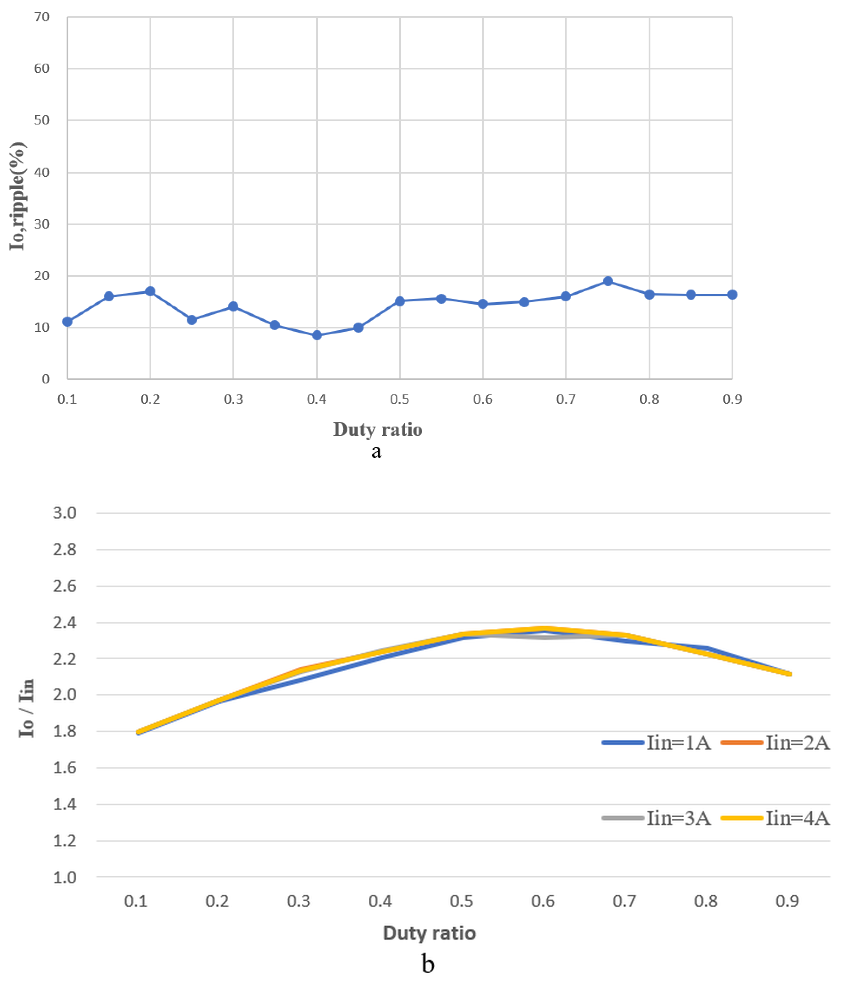
4.3. Current Conversion Ratio of Tapped-Inductor Boost Current Converter

Based on the Figure 12a experimental results, we observe that the current conversion ratio is around 2.2 times along with the duty ratios. This matches with the simulated results in Figure 7 and Figure 12a. Also, the experimental results agree with the Formulas (23)–(30). The new topology converts the output current mainly relying on the turns ratio of the tapped-inductor instead of the duty ratio of the switches. Hence, the current gain can remain stable and reliable even the value of the input current is changed. Moreover, based on Figure 12a, it can show that the current gains of the experiments and simulations have a similar trend. The effect of the input current I in is also investigated and shown in Figure 12b. Based on the Figure 12b results, it is observed that the values of the I in does not affect the current gain of the converter significantly. The current gain of the Tapped-inductor converter only changes slightly when the I in is changed. Moreover, the trend of the current gains changing were similar even they have different input currents. This can show that the performance of the new introduced converter is stable even under different input currents.

4.4. Comparison of Power Conversion Efficiency

Figure 13a shows that the power conversion efficiency of the tapped-inductor boost current converter can keep around 95% with duty ratio from 0.35 to 0.85. The range of duty ratio less than 0.35 and over 0.85 is not practical for real converters. The power conversion efficiency of the tapped-inductor was much higher when compared with the conventional boost current converter. The maximum power conversion efficiency of the conventional boost current converter can only acquire around 80% using the same design. Hence, it can be observed that the power conversion efficiency of Tapped-inductor boost current converter is much higher than that of the Conventional boost current converter. Figure 13b shows the theoretical behaviour which the loss and thermal variation of equivalent resistance of the capacitors and inductors has not been taken into account. Based on the Figure 13b results, it is observed that the tendency of the experimental and simulated results of the conventional boost and tapped-inductor converters are similar. Moreover, the experimental results only are slightly different from the simulated results because the loss in simulation has not considered all the passive losses. The input current I in effect has also been investigated in this paper. The Tapped-inductor boost current converter is simulated under different input current I in to explore the variation of the power conversion efficiency of the Tapped-inductor converter. Figure 13c shows that the power conversion efficiency has not been changed significantly even the I in is changed along with in the range from 1 to 4A. Moreover, the power conversion efficiency remains above 90% with the I in changed along from 1 to 4A.
The ohmic power losses in MOSFET S1 and S2 are given as
P S 1 = I 2 S 1 ( RMS ) R d s 1
P S 2 = I 2 S 2 ( RMS ) R d s 2
here, the R d s 1 and R d s 2 are the MOSFETs ON resistances for S 1 and S 2 respectively. Hence, the total power loss in the MOSFETs S 1 and S 2 can be shown as
P S = P S 1 + P S 2
Moreover, the power loss associated with the forward voltage drop of the Diode D 1 and D 2 are given as
P V F , D 1 = V F , D 1 I D 1 ( A V G )
P V F , D 2 = V F , D 2 I D 2 ( A V G )
the V F , D 1 and V F , D 2 represent the forward voltage drop of the Diode D 1 and D 2 respectively. Using (23) and (24), the total power loss in Diode D 1 and D 2 can be expressed as
P D = P V F , D 1 + P V F , D 2
The power losses in inductors can be expressed as
P N p = I 2 N P ( R M S ) R N p
P N s = I 2 N S ( R M S ) R N s
P L = I 2 R L ( R M S ) R L
here, R N p and R N s are the resistance of the Tapped-inductor and R L is the resistance of the inductive filter. Hence, the total power loss in converter can be shown as
P l o s s = P S + P D + P N p + P N s + P L
where P S is the MOSFETs losses, P D is the diodes losses, PNp is the primary winding loss of the tapped-inductor, P N s is the secondary winding loss of the tapped-inductor and P L is the output inductive filter loss. The Tapped-inductor boost current converter is affected by the power losses in the semiconductors and the passive elements. The analysis is simplified by considering semiconductor conduction losses and parasitic resistance losses. The efficiency is calculated by
η = P i n P l o s s P i n × 100
where the P in is the input power.

4.5. Comparison of Output Current Ripple

The percentage of the output current ripple Io,ripple
I o , r i p p l e = I o , m a x I o , m i n I o , a v g × 100
Figure 14a,b shows that the tapped-inductor boost current converter obtained less output current ripples along with the duty ratio from 0.35 to 0.85 when compared with the conventional boost current converter. Figure 14a,b shows that the new topology maintained the output current ripple I o , r i p p l e below 10% with the duty ratio range from 0.35 to 0.85. However, the conventional boost current converter did not succeed as the Figure 14a shown. The output current ripples of the conventional boost current converter are higher than the new introduced topology under some duty ratios as the Figure 14a The maximum output current ripple of the conventional boost current converter reaches nearly 15% when the duty ratio at 0.35 as Figure 14a shown. This can show that the performance of the Tapped-inductor boost current converter is much better than the conventional boost current converter. In Figure 14a,b, the experiments and the simulations for investigating the output current ripples of the Tapped-inductor boost current converter have been conducted. The results can show that the experimental results are close and similar to the simulation results. Although the simulated results are slightly different from the experimental results because the passive components’ ESR has not been considered. The simulation also extends the range to 0.1 and 0.9 because the simulation can test the extreme duty ratio such as around 0.1 and 0.9 where the experiment cannot. The tendency of the curves is similar for all cases.

4.6. Loading Effect

In this section, the loading effect of the new topology is examined including the output current ripple and current conversion ratio. All the parameters for the experimental setup were remain unchanged except for the case that the loading of the converter was changed to 10 Ω . Table 6 shows the parameters used. Figure 9 shows the circuit used for the test.
Figure 15a,b show the loading effect for the Tapped-inductor boost current converter. Figure 15a shows the experimental ripple at a fixed input current and output resistance. The ripple is around 10% to 20% that is acceptance for practical conversion. In Figure 15b, we observed that the current conversion ratio only had slightly changed even the output loading is doubled. These results can match with Formulas (23)–(30), the current conversion ratio depends on the turns ratio of the Tapped-inductor mainly. In the other words, the tapped-inductor boost current converter can remain the current conversion ratio in stable even the input current I in or the loading R is changed.

5. Conclusions

This paper has introduced a new topology for the Tapped-inductor boost current converter. The analysis has been thoroughly studied according to the theories, simulations and experiments. The current conversion ratio, output current ripple, power conversion efficiency, and the loading effect for this new topology have been investigated in this paper. The parasitic components of the new introduced topology have been also considered and analyzed. Based on the experimental results, it can show that the proposed converter can achieve high efficiency above 95% with the range of the duty ratio from 0.1 to 0.9. Moreover, the converter can keep the output current ripple at less than 10% of the average value in the range of the duty ratio under normal loading. The experimental results have also been compared with the simulations and the theories. A detailed analysis in both simulations and experiments between the introduced topology and the conventional boost current converter have been conducted. The analysis shows that, based on the output current ripple I o , r i p p l e , current conversion ratio and power conversion efficiency, the performance of the new proposed topology is highly preferable. The new introduced Tapped-inductor boost current converter not only has a simple construction, but also it has high efficiency, wide output range and good output performance. This new topology is suitable for the Photovoltaic systems to boost the output current from the solar array directly. This is a direct method since the solar array is a typical current source. The tapped-inductor boost current converter with high efficiency and wide output range is useful for the solar system needs. It also provides a simple control of the current and direct current mode control instead of a current loop. The proposed circuit can be used as a fast current mode controller. Furthermore, it can be used as the current sink applications such as LED driver and the motor torque driver.

Author Contributions

Methodology, system design, experiment and writing—original draft preparation, C.P.L.; methodology, supervision and writing—review, K.W.E.C. All authors have read and agreed to the published version of the manuscript.

Funding

This research was funded partly by the University Grant Council RGF under grant PolyU 152218/19E.

Acknowledgments

The authors wish to acknowledge the support provided by the members of Power Electronics Research Centre (PERC), Department of Electrical Engineering, The Hong Kong Polytechnic University.

Conflicts of Interest

The authors declare no conflict of interest.

References

  1. Ha, S.; Tae, S.; Kim, R. Energy Demand Forecast Models for Commercial Buildings in South Korea. Energies 2019, 12, 2313. [Google Scholar] [CrossRef] [Green Version]
  2. Aineto, D.; Iranzo-Sánchez, J.; Lemus-Zúñiga, L.G.; Onaindia, E.; Urchueguia, J.F. On the Influence of Renewable Energy Sources in Electricity Price Forecasting in the Iberian Market. Energies 2019, 12, 2082. [Google Scholar] [CrossRef] [Green Version]
  3. Gómez-Calvet, R.; Martinez-Duart, J.M. On the Assessment of the 2030 Power Sector Transition in Spain. Energies 2019, 12, 1369. [Google Scholar] [CrossRef] [Green Version]
  4. Jäger-Waldau, A. Snapshot of Photovoltaics—February 2019. Energies 2019, 12, 769. [Google Scholar] [CrossRef] [Green Version]
  5. Fu, B.; Ouyang, C.; Li, C.; Wang, J.; Gul, E. An Improved Mixed Integer Linear Programming Approach Based on Symmetry Diminishing for Unit Commitment of Hybrid Power System. Energies 2019, 12, 833. [Google Scholar] [CrossRef] [Green Version]
  6. Theuerl, S.; Herrmann, C.; Heiermann, M.; Grundmann, P.; Landwehr, N.; Kreidenweis, U.; Prochnow, A. The Future Agricultural Biogas Plant in Germany: A Vision. Energies 2019, 12, 396. [Google Scholar] [CrossRef] [Green Version]
  7. Khalifehei, K.; Azizyan, G.; Gualtieri, C. Analyzing the Performance of Wave-Energy Generator Systems (SSG) for the Southern Coasts of Iran, in the Persian Gulf and Oman Sea. Energies 2018, 11, 3209. [Google Scholar] [CrossRef] [Green Version]
  8. Lawrenz, L.; Xiong, B.; Lorenz, L.; Krumm, A.; Hosenfeld, H.; Burandt, T.; Löffler, K.; Oei, P.Y.; Von Hirschhausen, C. Exploring Energy Pathways for the Low-Carbon Transformation in India—A Model-Based Analysis. Energies 2018, 11, 3001. [Google Scholar] [CrossRef] [Green Version]
  9. Rey-Hernández, J.M.; Velasco-Gómez, E.; San José-Alonso, J.F.; Tejero-González, A.; González-González, S.L.; Rey-Martinez, F.J. Monitoring Data Study of the Performance of Renewable Energy Systems in a Near Zero Energy Building in Spain: A Case Study. Energies 2018, 11, 2979. [Google Scholar] [CrossRef] [Green Version]
  10. Simon, S.; Naegler, T.; Gils, H.C. Transformation towards a Renewable Energy System in Brazil and Mexico—Technological and Structural Options for Latin America. Energies 2018, 11, 907. [Google Scholar] [CrossRef] [Green Version]
  11. Wu, B.; Li, S.; Yao, L.; Smedley, K.M. A New Hybrid Boosting Converter for Renewable Energy Applications. IEEE Trans. Power Electron. 2016, 31, 1203–1215. [Google Scholar] [CrossRef]
  12. Sivakumar, S.; Sathik, M.J.; Manoj, P.S.; Sundararajan, G. An assessment on performance of DC–DC converters for renewable energy applications. Renew. Sustain. Energy Rev. 2016, 58, 1475–1485. [Google Scholar] [CrossRef]
  13. Mira, M.C.; Zhang, Z.; Knott, A.; Andersen, M.A.E. Analysis, Design, Modeling, and Control of an Interleaved-Boost Full-Bridge Three-Port Converter for Hybrid Renewable Energy Systems. IEEE Trans. Power Electron. 2017, 32, 1138–1155. [Google Scholar] [CrossRef] [Green Version]
  14. Das, M.; Agarwal, V. Design and Analysis of a High-Efficiency DC–DC Converter With Soft Switching Capability for Renewable Energy Applications Requiring High Voltage Gain. IEEE Trans. Ind. Electron. 2016, 63, 2936–2944. [Google Scholar] [CrossRef]
  15. Tseng, K.C.; Cheng, C.A.; Chen, C.T. High Step-Up Interleaved Boost Converter for Distributed Generation Using Renewable and Alternative Power Sources. IEEE J. Emerg. Sel. Top. Power Electron. 2017, 5, 713–722. [Google Scholar] [CrossRef]
  16. Cheng, K.W.E.; Ye, Y.-M. Duality approach to the study of switched-inductor power converters and its higher-order variations. IET Power Electron. 2015, 8, 489–496. [Google Scholar] [CrossRef]
  17. Li, S.; Cheng, K.W.E.; Ye, Y.; Shi, Z. Wide input and wide output topology analysis for tapped-inductor converters with consideration of parasitic elements. IET Power Electron. 2016, 9, 1952–1961. [Google Scholar] [CrossRef]
  18. Babaei, E.; Feyzi, H.; Gholizadeh-Roshanagh, R. Generalized Switched-Inductor Based Buck-Boost Z-H Converter. Iran. J. Electr. Electron. Eng. 2017, 13, 340–352. [Google Scholar]
  19. Barzegarkhoo, R.; Moradzadeh, M.; Zamiri, E.; Madadi Kojabadi, H.; Blaabjerg, F. A New Boost Switched-Capacitor Multilevel Converter With Reduced Circuit Devices. IEEE Trans. Power Electron. 2018, 33, 6738–6754. [Google Scholar] [CrossRef]
  20. Ye, Y.; Cheng, K.W.E.; Chen, S. A High Step-up PWM DC-DC Converter With Coupled-Inductor and Resonant Switched-Capacitor. IEEE Trans. Power Electron. 2017, 32, 7739–7749. [Google Scholar] [CrossRef]
  21. Mondzik, A.; Waradzyn, Z.; Stala, R.; Penczek, A. High efficiency switched capacitor voltage doubler with planar core-based resonant choke. In Proceedings of the 2016 10th International Conference on Compatibility, Power Electronics and Power Engineering (CPE-POWERENG), Bydgoszcz, Poland, 29 June–1 July 2016; pp. 402–409. [Google Scholar]
  22. Schaef, C.; Stauth, J.T. A Highly Integrated Series-Parallel Switched-Capacitor Converter With 12 V Input and Quasi-Resonant Voltage-Mode Regulation. IEEE J. Emerg. Sel. Top. Power Electron. 2018, 6, 456–464. [Google Scholar] [CrossRef]
  23. Ye, Y.; Cheng, K.W.E. Modeling and Analysis of Series-Parallel Switched-Capacitor Voltage Equalizer for Battery/Supercapacitor Strings. IEEE J. Emerg. Sel. Top. Power Electron. 2015, 3, 977–983. [Google Scholar] [CrossRef]
  24. Abraham, C.; Jose, B.R.; Mathew, J.; Evzelman, M. Modelling, simulation and experimental investigation of a new two input, series-parallel switched capacitor converter. IET Power Electron. 2017, 10, 368–376. [Google Scholar] [CrossRef]
  25. Li, S.; Kang, X.; Zheng, Y.; Ma, K.S. Analysis and Design of the Ladder Resonant Switched-Capacitor Converters for Regulated Output Voltage Applications. IEEE Trans. Ind. Electron. 2017, 64, 7769–7779. [Google Scholar] [CrossRef]
  26. Alishah, R.S.; Hosseini, S.H.; Babaei, E.; Sabahi, M. Optimal Design of New Cascaded Switch-Ladder Multilevel Inverter Structure. IEEE Trans. Ind. Electron. 2017, 64, 2072–2080. [Google Scholar] [CrossRef]
  27. Liu, H.C.; Li, F. Novel High Step-Up DC-DC Converter With an Active Coupled-Inductor Network for a Sustainable Energy System. IEEE Trans. Power Electron. 2015, 30, 6476–6482. [Google Scholar] [CrossRef]
  28. Liu, H.; Li, F. A Novel High Step-up Converter with a Quasi-active Switched-Inductor Structure for Renewable Energy Systems. IEEE Trans. Power Electron. 2016, 31, 5030–5039. [Google Scholar] [CrossRef]
  29. Nejad, M.; Poorali, B.; Adib, E. New cascade boost converter with reduced losses. IET Power Electron. 2016, 9, 1213–1219. [Google Scholar] [CrossRef]
  30. Chincholkar, S.H.; Jiang, W.; Chan, C.Y. An Improved PWM-Based Sliding-Mode Controller for a DC-DC Cascade Boost Converter. IEEE Trans. Circuits Syst. Express Briefs 2018, 65, 1639–1643. [Google Scholar] [CrossRef]
  31. Lopez-Santos, O.; Martinez-Salamero, L.; Garcia, G.; Valderrama-Blavi, H.; Zambrano-Prada, D.A. Steady-State Analysis of Inductor Conduction Modes in the Quadratic Boost Converter. IEEE Trans. Power Electron. 2017, 32, 2253–2264. [Google Scholar] [CrossRef] [Green Version]
  32. Valdez-Resendiz, J.E.; Rosas-Caro, J.C.; Mayo-Maldonado, J.C.; Llamas-Terres, A. Quadratic boost converter based on stackable switching stages. IET Power Electron. 2018, 11, 1373–1381. [Google Scholar] [CrossRef]
  33. Ahmad, A.; Bussa, V.K.; Singh, R.K.; Mahanty, R. Quadratic boost derived hybrid multi-output converter. IET Power Electron. 2017, 10, 2042–2054. [Google Scholar] [CrossRef]
  34. Zhang, N.; Sutanto, D.; Muttaqi, K.M.; Zhang, B.; Qiu, D. High-voltage-gain quadratic boost converter with voltage multiplier. IET Power Electron. 2015, 8, 2511–2519. [Google Scholar] [CrossRef]
  35. Leyva-Ramos, J.; Mota-Varona, R.; Ortiz-Lopez, M.G.; Diaz-Saldierna, L.H.; Langarica-Cordoba, D. Control Strategy of a Quadratic Boost Converter With Voltage Multiplier Cell for High-Voltage Gain. IEEE J. Emerg. Sel. Top. Power Electron. 2017, 5, 1761–1770. [Google Scholar] [CrossRef]
  36. Abramovitz, A.; Yao, J.; Smedley, K. Unified Modeling of PWM Converters With Regular or Tapped Inductors Using TIS-SFG Approach. IEEE Trans. Power Electron. 2016, 31, 1702–1716. [Google Scholar] [CrossRef]
  37. Bez, F.; Bonanno, G.; Corradini, L.; Garbossa, C. Control Technique for Reliable Operation of the Synchronous Series Capacitor Tapped Inductor Converter. IEEE Trans. Power Electron. 2019, 34, 8150–8161. [Google Scholar] [CrossRef]
  38. Vázquez, N.; Medina, F.; Hernández, C.; Arau, J.; Vázquez, E. Double tapped-inductor boost converter. IET Power Electron. 2015, 8, 831–840. [Google Scholar] [CrossRef]
  39. Choi, J.; Kim, J.S.; Lee, G.; Kim, K.D.; Kang, F.S. Cascaded dc-to-dc converter employing a tapped-inductor for high voltage boosting ratio. In Proceedings of the IECON 2015—41st Annual Conference of the IEEE Industrial Electronics Society, Yokohama, Japan, 9–12 November 2015; pp. 932–937. [Google Scholar]
  40. Liu, Y.; Sekiguchi, R.; Sano, Y. Study on Improving Precision of Analysis of Boost Ratio and Power Efficiency of Tapped-Inductor DC–DC Converter Circuit. Electr. Eng. Jpn. 2018, 202, 3–20. [Google Scholar] [CrossRef]
Figure 1. Tapped-inductor buck current converter topology and its operation states. (a) Tapped-inductor buck current converter topology; (b) S2 in on-state and S1 in off-state; (c) S2 in off-state and S1 in on-state.
Energies 14 00888 g001
Figure 2. Tapped-inductor boost current converter topology and its operation states. (a) Tapped-inductor boost current converter topology; (b) S 2 in on-state and S 1 in off-state; (c) S 2 in off-state and S 1 in on-state.
Energies 14 00888 g002
Figure 3. Tapped-inductor buck-boost current converter topology and its operation states. (a) Tapped-inductor buck-boost current converter topology; (b) S 1 in on-state and S 2 in off-state; (c) S 1 in off-state and S 2 in on-state.
Energies 14 00888 g003aEnergies 14 00888 g003b
Figure 4. Conventional Boost current converter topology and its operation states. (a) Conventional Boost current converter topology; (b) S1 in on-state; (c) S1 in off-state.
Energies 14 00888 g004
Figure 5. Characteristic of the Conventional Boost current converter, the Current gain with duty ratio of conventional boost current converter.
Energies 14 00888 g005
Figure 6. Tapped-inductor Boost current converter topology and its operation states. (a) Tapped-inductor Boost current converter topology; (b) S1 is in off-state and S2 is in on-state; (c) S1 is in on-state and S2 is in off-state.
Energies 14 00888 g006
Figure 7. Current gain with turns ratio of Tapped-inductor boost current converter.
Energies 14 00888 g007
Figure 8. Tapped-inductor boost current converter topology with parasitic components.
Energies 14 00888 g008
Figure 9. Tapped-inductor Boost current converter topology.
Energies 14 00888 g009
Figure 10. Measured waveforms of the experimental of the tapped-inductor boost current converter. (a) Top trace: Iout (5 μs/500 mA/div); middle trace: VGS of S1 switch (5 μs/20 V/div); bottom trace: VDS of S1 (5 μs/100 V/div); (b) Top trace: Iout (5 μs/500 mA/div); middle trace: VGS of S2 switch (5 μs/20 V/div); bottom trace: VDS of S2 (5 μs/20 V/div); (c) Top trace: VGS of S1 switch (5 μs/10 V/div); bottom trace: VDS of S2 (5 μs/10 V/div).
Energies 14 00888 g010
Figure 11. Conventional boost current converter topology.
Energies 14 00888 g011
Figure 12. Analysis the current gain of the Tapped-inductor boost current converter with duty ratio. (a) Comparison of the current gain in between the simulated results and the experimental results ( I in = 1 A and R = 5 Ω ); (b) Simulated results of the current gain with different input currents.
Energies 14 00888 g012
Figure 13. Comparison of power conversion efficiency. (a) Compared with the experimental results of the Conventional and Tapped-inductor boost current converters under Iin = 1 A, R = 5 Ω ; (b) Compared with the simulated results of the Conventional and Tapped-inductor boost current converters under Iin = 1 A, R = 5 Ω ; (c) Compared with the simulated results with different input currents Iin with R = 5 Ω .
Energies 14 00888 g013
Figure 14. (a) Compared with the experimental results of the Output current ripples of the Conventional and Tapped-inductor boost current converters under Iin = 1 A and R = 5 Ω ; (b) Compared with the simulated results of the Output current ripples of the Conventional and Tapped-inductor boost current converters under I in = 1 A and R = 5 Ω .
Energies 14 00888 g014
Figure 15. Experimental and simulated results of Tapped-inductor boost current converter with loading effect analysis. (a) Output current ripple of the converter under Iin = 1 A and R = 10 Ω ; (b) Current conversion ratio of the converter with different Iin.
Energies 14 00888 g015
Table 1. Parameters used in simulation—Conventional boost current converter.
Duty Ratio0.1–0.9
Load R ( Ω )5
Capacitance C (F)30
Inductance L (mH)1.53
Table 2. Parameters used in simulations—Tapped-inductor boost current converter.
Load R ( Ω )5
Switching frequency (kHz)100
Turns Ratio of the tapped-inductor0.7
Output Inductive filter L (mH)1.53
Table 3. Parasitic components used in simulations—Tapped-inductor boost current converter.
R d s 1 (m Ω )58
R d s 2 (m Ω )58
R N p ( Ω )0.4
R N s ( Ω )0.2
R L ( Ω )0.1
v F , D 1 (V)0.5
v F , D 2 (V)0.5
Table 4. Parameters used in experiments.
Duty Ratio0.1–0.9
Load R ( Ω )5
Switching frequency (kHz)100
Turns Ratio of the tapped-inductor0.7
Primary inductance, Np (mH)62
Secondary inductance, Ns (mH)3
Output inductive filter (mH)1.53
Switches S1, Rds1 (m Ω )58
Switches S2, Rds2 (m Ω )58
Table 5. Parameters used in experiments.
Duty Ratio0.1–0.9
Load R ( Ω )5
Switching frequency (kHz)100
Capacitor C (F)30
Output inductive filter L (mH)1.53
Table 6. Parameters used in experiments.
Duty Ratio0.1–0.9
Load R ( Ω )10
Switching frequency (kHz)100
Turns Ratio of the tapped-inductor0.7
Primary inductance, Np (mH)62
Secondary inductance, Ns (mH)3
Output inductive filter L (mH)1.53
Switches S1,Rds1 (m Ω )58
Switches S2,Rds2 (m Ω )58
Publisher’s Note: MDPI stays neutral with regard to jurisdictional claims in published maps and institutional affiliations.

