
Novel Interleaved High Gain Boost Converter Using Switched Capacitor


Abstract
:1. Introduction
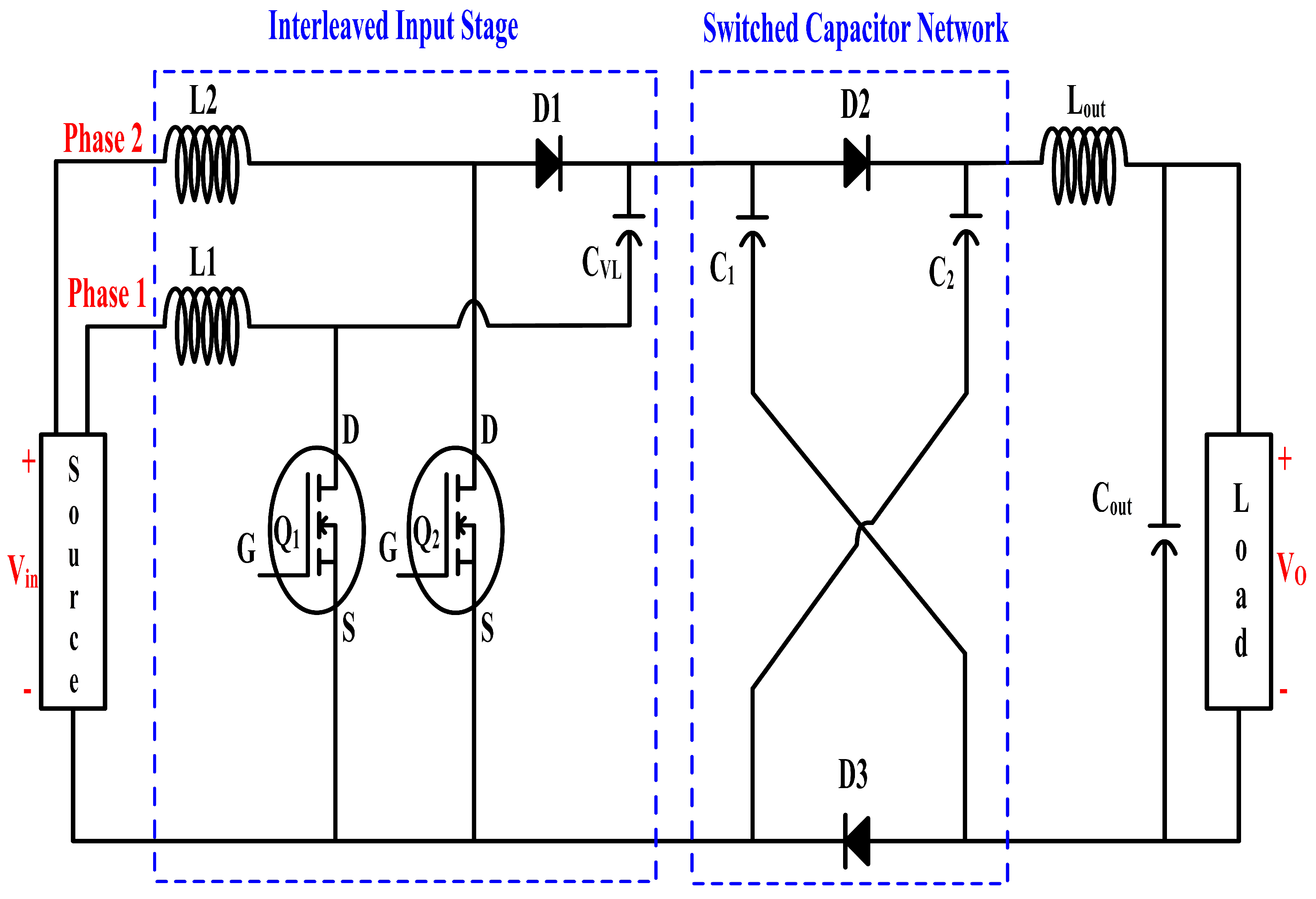
1.1. Power Circuit
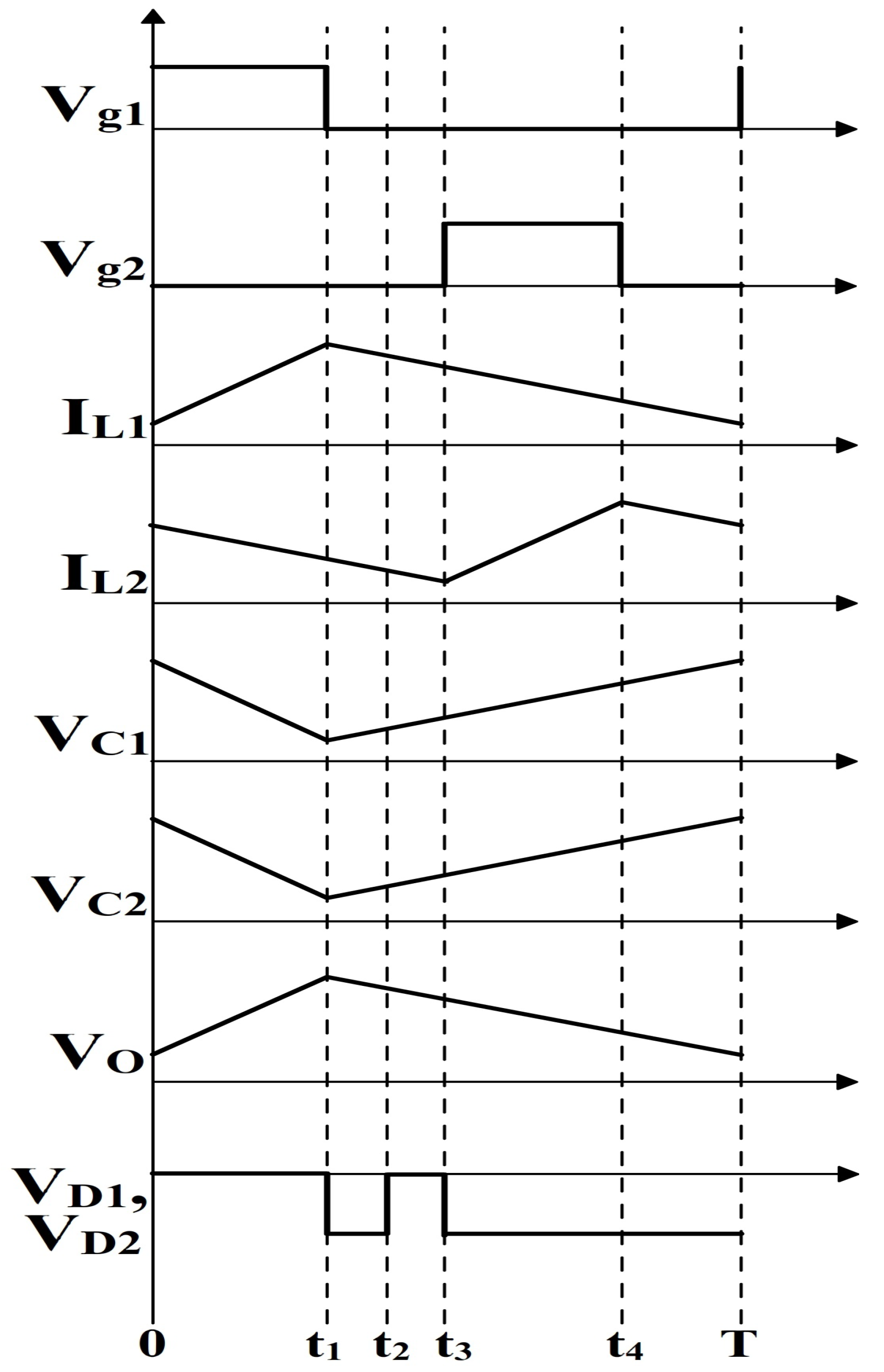
1.2. Steady State Modes of Operation
1.2.1. Mode 1 ()
1.2.2. Mode 2 ()
1.2.3. Mode 3 ()
1.2.4. Mode 4 ()
1.2.5. Mode 5 ()
2. Analysis of the Proposed Converter
2.1. Interleaved Stage Gain
2.2. Switched Capacitor Network Gain
2.3. Overall Gain
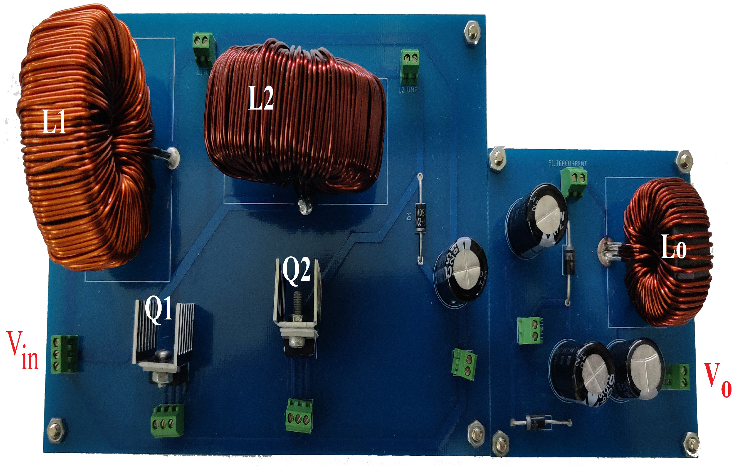
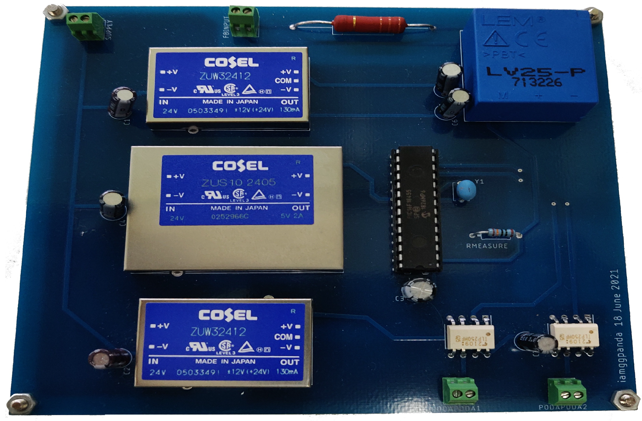
3. Converter Design
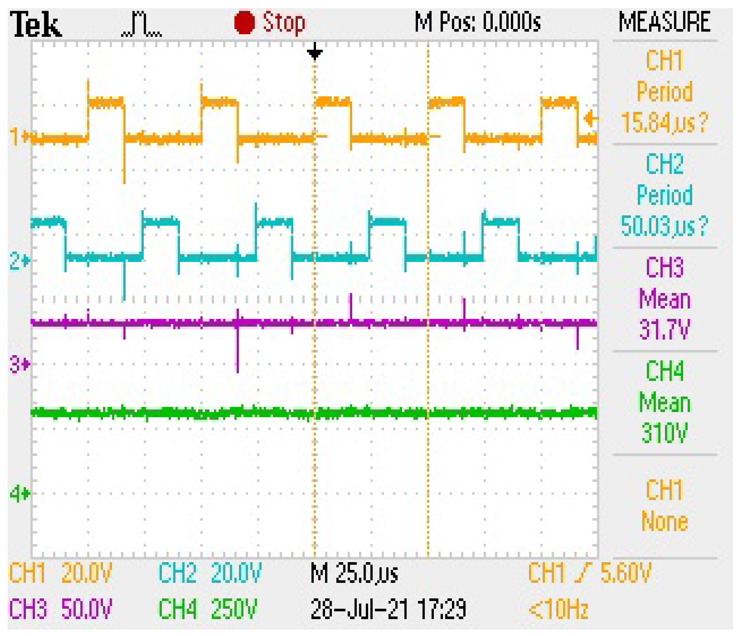
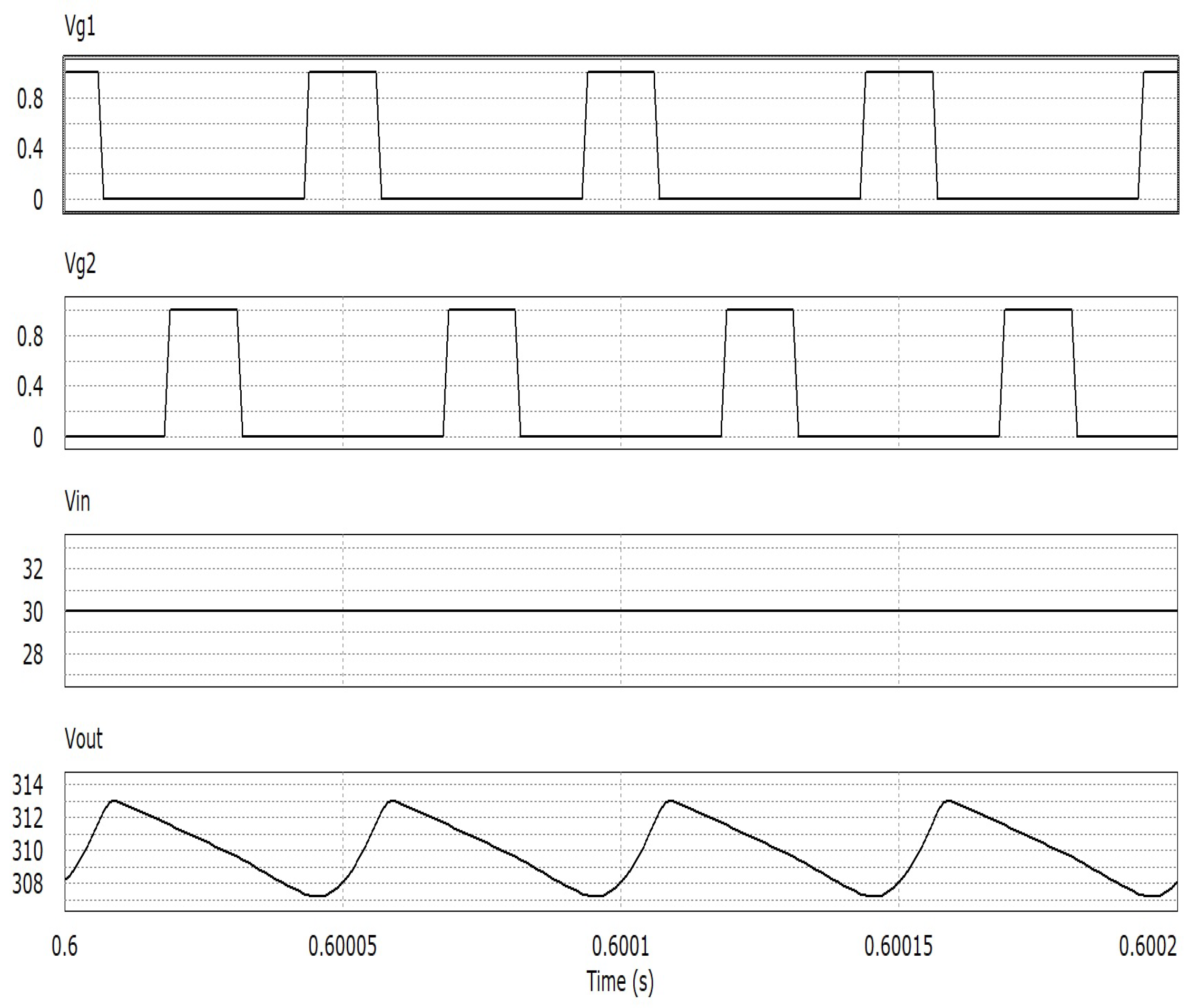
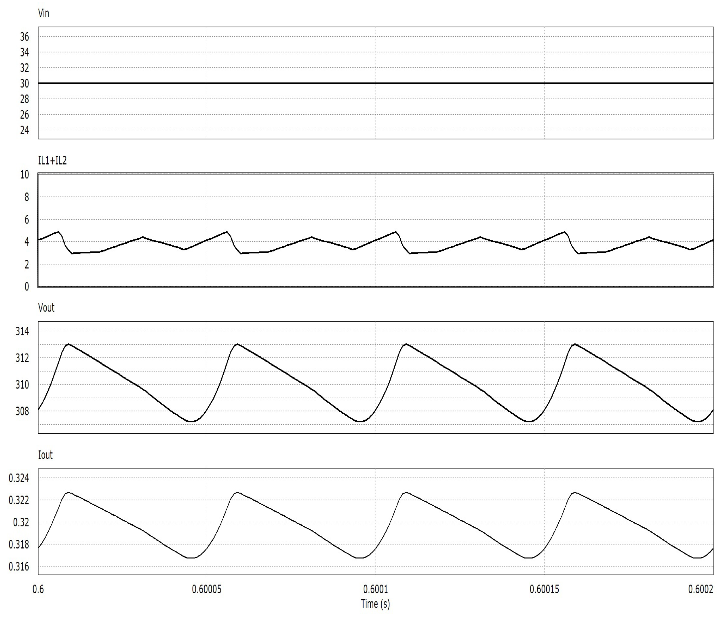
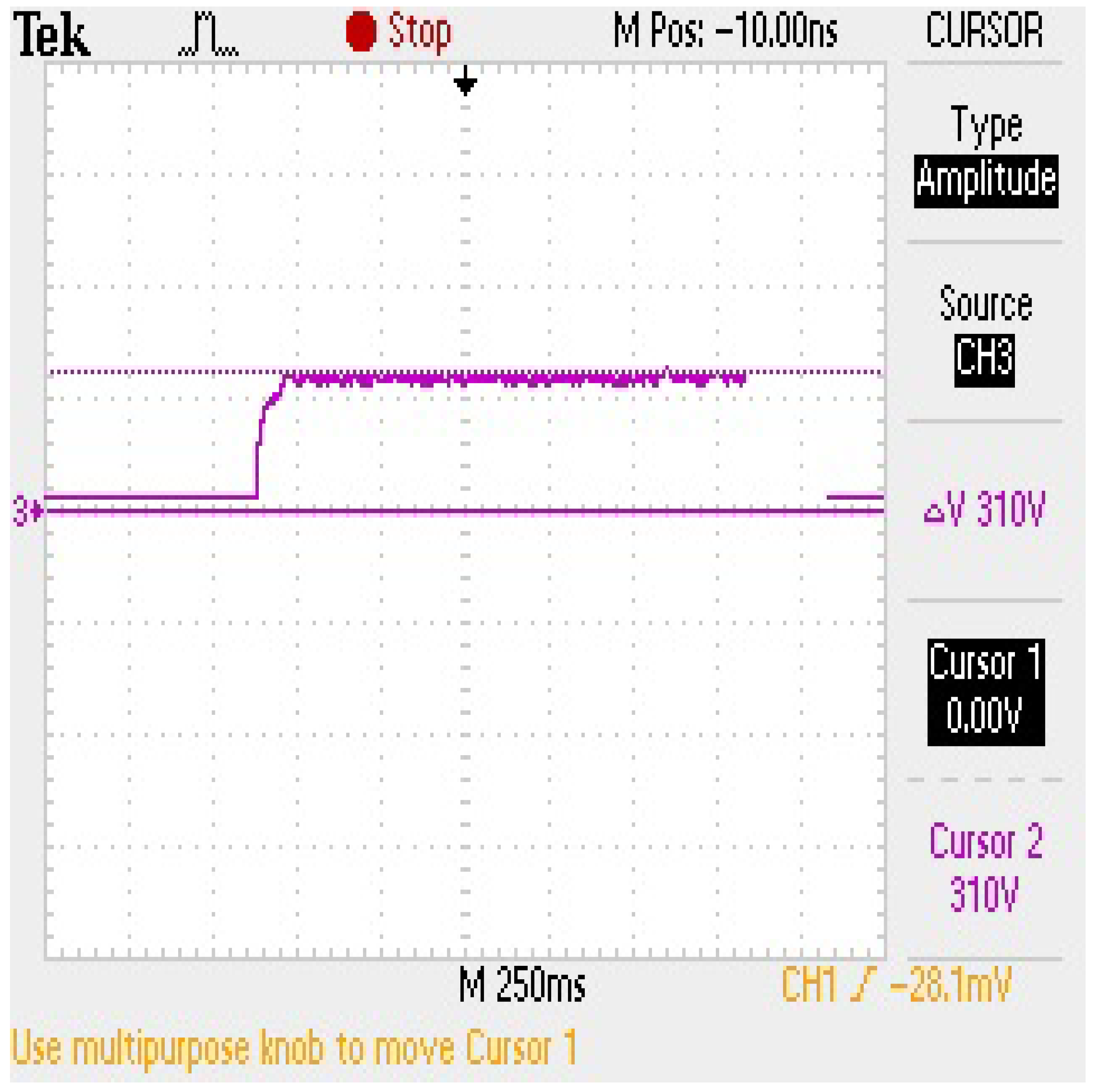
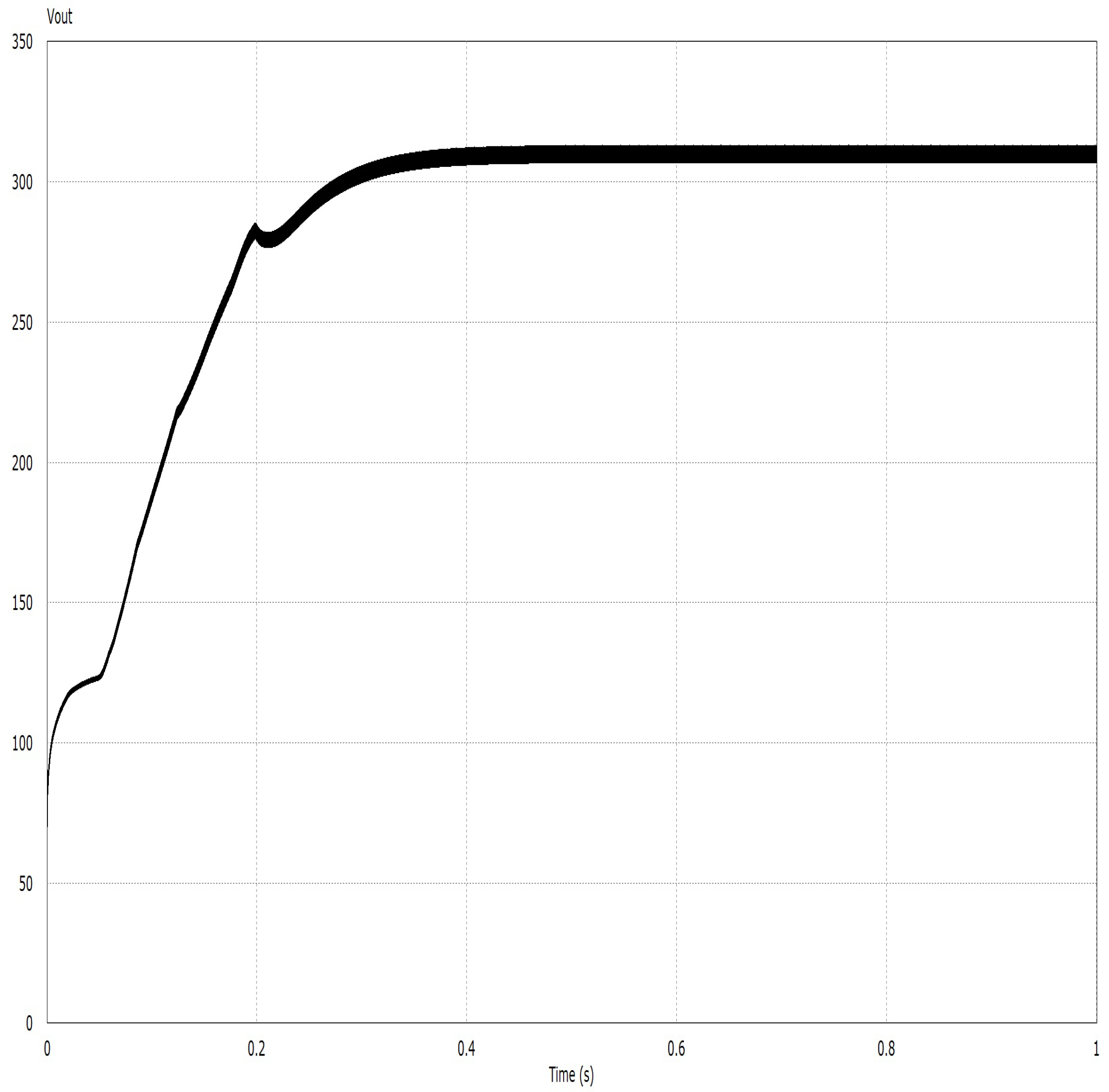
4. Results and Discussion
5. Conclusions
Author Contributions
Funding
Institutional Review Board Statement
Informed Consent Statement
Conflicts of Interest
References
- Luo, F.; Zhang, T.; Mi, Z.; Li, F.; Bai, L.; Liu, G.; Sun, Q.; Wang, X. Study on low-carbon comprehensive benefits of grid-connected photovoltaic generation. In Proceedings of the 2015 IEEE Power & Energy Society General Meeting, Denver, CO, USA, 26–30 July 2015; pp. 1–5. [Google Scholar]
- Köberle, A.C.; Gernaat, D.E.; van Vuuren, D.P. Assessing current and future techno-economic potential of concentrated solar power and photovoltaic electricity generation. Energy 2015, 89, 739–756. [Google Scholar] [CrossRef] [Green Version]
- Das, M.; Agarwal, V. Novel high-performance stand-alone solar PV system with high-gain high-efficiency DC–DC converter power stages. IEEE Trans. Ind. Appl. 2015, 51, 4718–4728. [Google Scholar] [CrossRef]
- Silvestre, S.; Chouder, A. Effects of shadowing on photovoltaic module performance. Prog. Photovolt. Res. Appl. 2008, 16, 141–149. [Google Scholar] [CrossRef]
- Eltamaly, A.M. Performance of smart maximum power point tracker under partial shading conditions of photovoltaic systems. J. Renew. Sustain. Energy 2015, 7, 043141. [Google Scholar] [CrossRef]
- Sullivan, C.R.; Awerbuch, J.J.; Latham, A.M. Decrease in photovoltaic power output from ripple: Simple general calculation and the effect of partial shading. IEEE Trans. Power Electron. 2012, 28, 740–747. [Google Scholar] [CrossRef]
- Erickson, R.W.; Maksimovic, D. Fundamentals of Power Electronics; Springer Science & Business Media: Berlin/Heidelberg, Germany, 2007. [Google Scholar]
- Maksimovic, D.; Cuk, S. Switching converters with wide DC conversion range. IEEE Trans. Power Electron. 1991, 6, 151–157. [Google Scholar] [CrossRef]
- Sreekanth, T.; Lakshminarasamma, N.; Mishra, M.K. A single-stage grid-connected high gain buck–boost inverter with maximum power point tracking. IEEE Trans. Energy Convers. 2016, 32, 330–339. [Google Scholar] [CrossRef]
- Shanthi, T.; Prabha, S.U.; Sundaramoorthy, K. Non-Isolated n-Stage High Step-up DC-DC Converter for Low Voltage DC Source Integration. IEEE Trans. Energy Convers. 2021, 36, 1625–1634. [Google Scholar] [CrossRef]
- Wu, T.F.; Chen, Y.C.; Yang, J.G.; Huang, Y.C.; Shyu, S.S.; Lee, C.L. 1.5 kW isolated bi-directional DC-DC converter with a flyback snubber. In Proceedings of the 2009 International Conference on Power Electronics and Drive Systems (PEDS), Taipei, Taiwan, 2–5 November 2009; pp. 164–169. [Google Scholar] [CrossRef] [Green Version]
- Wu, H.; Mu, T.; Ge, H.; Xing, Y. Full-Range Soft-Switching-Isolated Buck-Boost Converters With Integrated Interleaved Boost Converter and Phase-Shifted Control. IEEE Trans. Power Electron. 2016, 31, 987–999. [Google Scholar] [CrossRef]
- Andrade, A.M.S.S.; Mattos, E.; Schuch, L.; Hey, H.L.; da Silva Martins, M.L. Synthesis and comparative analysis of very high step-up DC–DC converters adopting coupled-inductor and voltage multiplier cells. IEEE Trans. Power Electron. 2017, 33, 5880–5897. [Google Scholar] [CrossRef]
- Axelrod, B.; Berkovich, Y.; Ioinovici, A. Transformerless DC-DC converters with a very high DC line-to-load voltage ratio. In Proceedings of the 2003 International Symposium on Circuits and Systems, Bangkok, Thailand, 25–28 May 2003; Volume 3, p. III. [Google Scholar]
- Girish Ganesan, R.; Prabhakar, M. Multi-level dc-dc converter for high gain applications. Int. J. Power Electron. Driv. Syst. 2013, 3, 365–373. [Google Scholar]
- Prudente, M.; Pfitscher, L.L.; Emmendoerfer, G.; Romaneli, E.F.; Gules, R. Voltage multiplier cells applied to non-isolated DC–DC converters. IEEE Trans. Power Electron. 2008, 23, 871–887. [Google Scholar] [CrossRef]
- Girish Ganesan, R.; Prabhakar, M. Non-isolated high step-up interleaved boost converter. Int. J. Power Electron. 2014, 6, 288–303. [Google Scholar] [CrossRef]
- Chen, S.M.; Liang, T.J.; Yang, L.S.; Chen, J.F. A cascaded high step-up DC–DC converter with single switch for microsource applications. IEEE Trans. Power Electron. 2010, 26, 1146–1153. [Google Scholar] [CrossRef]
- An, L.; Lu, D.D.C. Analysis of DC bus capacitor current ripple reduction in basic DC/DC cascaded two-stage power converters. IEEE Trans. Ind. Electron. 2016, 63, 7467–7477. [Google Scholar] [CrossRef]
- Sivasankar, G.; Vidhyaa, K.; Anitha, E.; Kumar, B.A.; Vairaprakash, P. Application of luo converter and multilevel cascaded converter for grid integration of solar pv systems. In Proceedings of the 2016 International Conference on Circuit, Power and Computing Technologies (ICCPCT), Nagercoil, India, 18–19 March 2016; pp. 1–6. [Google Scholar]
- Zhao, J.; Iu, H.H.; Fernando, T. The design of cascaded DC-DC converters with single-switch PWM and PFM for standalone PV power applications. In Proceedings of the 2017 IEEE 3rd International Future Energy Electronics Conference and ECCE Asia (IFEEC 2017-ECCE Asia), Kaohsiung, Taiwan, 4–7 June 2017; pp. 122–126. [Google Scholar]
- Xie, F.; Zhang, B.; Qiu, D.; Jiang, Y. Non-linear dynamic behaviours of DC cascaded converters system with multi-load converters. IET Power Electron. 2016, 9, 1093–1102. [Google Scholar] [CrossRef]
- Axelrod, B.; Berkovich, Y.; Ioinovici, A. Switched-capacitor/switched-inductor structures for getting transformerless hybrid DC–DC PWM converters. IEEE Trans. Circuits Syst. I Regul. Pap. 2008, 55, 687–696. [Google Scholar] [CrossRef]
- Liccardo, F.; Marino, P.; Torre, G.; Triggianese, M. Interleaved dc-dc Converters for Photovoltaic Modules. In Proceedings of the 2007 International Conference on Clean Electrical Power, Capri, Italy, 21–23 May 2007; pp. 201–207. [Google Scholar] [CrossRef]
- Ramabadran, R.; Balaji, K.; Raj, S.; Logeshwaran, V. Comparison of Interleaved Boost Converter Configurations for Solar Photovoltaic System Interface. J. Eng. Res. 2013, 10, 87–98. [Google Scholar] [CrossRef] [Green Version]
- Prasanth, P.; Ramalingam, S. Investigation Of Four Phase Interleaved Boost Converter under Open Loop and Closed Loop Control Schemes for Battery Charging Applications. Int. J. Adv. Mater. Sci. Eng. 2016, 5, 11–20. [Google Scholar] [CrossRef]
- Farh, H.M.H.; Othman, M.F.; Eltamaly, A.M.; Al-Saud, M.S. Maximum Power Extraction from a Partially Shaded PV System Using an Interleaved Boost Converter. Energies 2018, 11, 2543. [Google Scholar] [CrossRef] [Green Version]
- Farh, H.M.; Eltamaly, A.M.; Al-Saud, M.S. Interleaved boost converter for global maximum power extraction from the photovoltaic system under partial shading. IET Renew. Power Gener. 2019, 13, 1232–1238. [Google Scholar] [CrossRef]
- Lee, P.W.; Lee, Y.S.; Cheng, D.; Liu, X.C. Steady-state analysis of an interleaved boost converter with coupled inductors. IEEE Trans. Ind. Electron. 2000, 47, 787–795. [Google Scholar] [CrossRef]
- Arango, E.; Ramos-Paja, C.A.; Calvente, J.; Giral, R.; Serna, S. Asymmetrical Interleaved DC/DC Switching Converters for Photovoltaic and Fuel Cell Applications—Part 1: Circuit Generation, Analysis and Design. Energies 2012, 5, 4590–4623. [Google Scholar] [CrossRef] [Green Version]
- Muhammad, M.; Armstrong, M.; Elgendy, M.A. A Nonisolated Interleaved Boost Converter for High-Voltage Gain Applications. IEEE J. Emerg. Sel. Top. Power Electron. 2016, 4, 352–362. [Google Scholar] [CrossRef] [Green Version]


| Parameter | Value/Description |
|---|---|
| 300 μH | |
| 300 μH | |
| 47 μF/250 V | |
| 47 μF/250 V | |
| 47 μF/250 V | |
| 20 μH | |
| 22 μF/350 V | |
| Switches and | FDP2532 |
| Diodes , and | SBYV27 |
| Voltage Sensor | LV25-P |
| Controller | Microchip PIC16F455 |
| MOSFET Drivers | TLP250 |
| Switching Frequency | 20 kHz |
Publisher’s Note: MDPI stays neutral with regard to jurisdictional claims in published maps and institutional affiliations. |
© 2021 by the authors. Licensee MDPI, Basel, Switzerland. This article is an open access article distributed under the terms and conditions of the Creative Commons Attribution (CC BY) license (https://creativecommons.org/licenses/by/4.0/).
Share and Cite
Ramanathan, G.G.; Urasaki, N. Novel Interleaved High Gain Boost Converter Using Switched Capacitor. Energies 2021, 14, 8091. https://doi.org/10.3390/en14238091
Ramanathan GG, Urasaki N. Novel Interleaved High Gain Boost Converter Using Switched Capacitor. Energies. 2021; 14(23):8091. https://doi.org/10.3390/en14238091
Chicago/Turabian StyleRamanathan, Girish Ganesan, and Naomitsu Urasaki. 2021. "Novel Interleaved High Gain Boost Converter Using Switched Capacitor" Energies 14, no. 23: 8091. https://doi.org/10.3390/en14238091
APA StyleRamanathan, G. G., & Urasaki, N. (2021). Novel Interleaved High Gain Boost Converter Using Switched Capacitor. Energies, 14(23), 8091. https://doi.org/10.3390/en14238091