Article

Monolithic Perovskite/Silicon-Heterojunction Tandem Solar Cells with Nanocrystalline Si/SiOx Tunnel Junction

1
Italian National Agency for New Technologies, Energy and Sustainable Economic Development (ENEA), Portici Research Center, Piazzale E. Fermi, 80055 Portici, Italy
2
Department of Chemical Sciences, Monte Sant’Angelo Campus, University of Naples Federico II, Via Cinthia 21, 80126 Naples, Italy
*
Author to whom correspondence should be addressed.
Energies 2021, 14(22), 7684; https://doi.org/10.3390/en14227684
Submission received: 19 October 2021 / Revised: 12 November 2021 / Accepted: 15 November 2021 / Published: 17 November 2021

Abstract

:
Perovskite/silicon tandem solar cells have strong potential for high efficiency and low cost photovoltaics. In monolithic (two-terminal) configurations, one key element is the interconnection region of the two subcells, which should be designed for optimal light management and prevention of parasitic p/n junctions. We investigated monolithic perovskite/silicon-heterojunction (SHJ) tandem solar cells with a p/n nanocrystalline silicon/silicon-oxide recombination junction for improved infrared light management. This design can additionally provide for resilience to shunts and simplified cell processing. We probed modified SHJ solar cells, made from double-side polished n-type Si wafers, which included the proposed front-side p/n tunnel junction with the p-type film simultaneously functioning as selective charge transport layer for the SHJ bottom cell, trying different thicknesses for the n-type layer. Full tandem devices were then tested, by applying a planar n-i-p mixed-cation mixed-halide perovskite top cell, fabricated via low temperature solution methods to be compatible with the processed Si wafer. We demonstrate the feasibility of this tandem cell configuration over a 1 cm2 area with negligible J-V hysteresis and a VOC ~1.8 V, matching the sum of the VOC-s contributed by the two components.

1. Introduction

Solar energy is among the best options for tackling climate change, and photovoltaics (PV) in particular may strongly contribute to satisfy the growing electricity demand while meeting the needed decarbonization. The PV industry has already demonstrated exponential growth, technological advancements, significant cost reductions, and now heads to multi-terawatt scales of annual production [1]. Meanwhile, extensive research is being carried out worldwide in the solar energy fields, with solar cells among the hottest topics [2]. Specifically, tandem solar cells combining lead halide perovskite and silicon subcells are under intense investigation as a viable solution for high efficiency and low cost photovoltaics, with theoretical limiting efficiency (with Auger recombination) above 43% [3] and recent certified efficiencies already approaching 30% for the monolithic design [4,5,6]. On the one hand, building on favorable material properties, perovskites have already demonstrated efficiencies exceeding 25% [4,7] thanks to significant advances in the understanding of defects and recombination mechanisms and in related practical implementations. Different formulations are under development. In particular, in view of tandem applications, compositions with mixed-cations and mixed-halides (typically I and Br) are mostly applied as they allow for bandgap tuning in the proper range (ideally around 1.7 eV to match with a silicon bottom cell bandgap of 1.1 eV [3,8]) by means of fine-adjustments of the elemental composition [5,6,9,10]. Besides the bandgap tuning, mixed-cation compositions, such as the triple cation mixing inorganic Cs with organic methylammonium (MA) and formamidinium (FA), also offer improved stability and robustness against variations in processing conditions, enabling more reproducible device performance [11].
As for the bottom counterpart, silicon heterojunction (SHJ) solar cells are the most frequent choice, thanks to excellent performance metrics such as the high open circuit voltage over 740 mV in record cells [4], enabled by amorphous silicon passivation. The SHJ technology has fully demonstrated to be a very effective concept for high-efficiency Si-based photovoltaics, with the world record efficiency of 26.7% achieved with the back-contact design [12] and efficiencies above 25% on full size n-type M2 c-Si wafer with both-side contact design [13]. In addition, SHJ solar cells feature a flexible architecture with wide variety of options (n or p wafer type, both polarities possible, standard, or bifacial design, back contact scheme, easy means to introduce novel carrier selective contacts) [14], thus opening for different tandem cell designs.
Together with the component cells, another key element for a good monolithic tandem cell is the interconnection region, where carriers from one subcell should recombine with carriers of opposite sign from the other subcell without introducing losses. This component plays electrical and optical roles and should be designed for optimal light management and prevention of parasitic p/n junctions [15]. In perovskite/SHJ tandem cells, often a single film of transparent conductive oxides (TCO), typically indium tin oxide (ITO), is included as recombination layer in between top and bottom component [16,17,18]. Although effective, this layer introduces some drawbacks, like reflection losses at the interface with Si, due to mismatched refractive index, and parasitic absorption losses at long wavelengths due to free-carrier absorption. Therefore, the layer should be kept thin. The combination of thin TCO and an optical interlayer with higher refractive index (~2.6 at 800 nm) has been recently proposed for improved infrared light management and applied also in record tandem solar cells [5,10]. Alternatively, the integration of a p/n recombination junction made of higher-index doped nanocrystalline Si has been proposed as a replacement of the TCO recombination layer [9,19].
In this work, we focus on a p/n tunnel junction based on doped nanocrystalline silicon/silicon-oxide layers deposited by plasma enhanced chemical vapor deposition (PECVD), building on the approaches of references [9,10,19]. This component is meant to act as an interband tunnel junction [15]. In particular, we investigated the feasibility of a simple tunnel junction scheme constituted by a p/n bilayer with the first layer (p-type nanocrystalline silicon, (p)nc-Si) primarily acting as selective charge transport layer for the SHJ bottom cell and the second layer (silicon-rich n-type nanocrystalline silicon-oxide, (n)nc-SiOx, with refractive index ~3.0 at 800 nm) included as interconnection layer with optical and electrical functionalities. A key feature of the (n)nc-SiOx material is its mixed-phase structure that allows for enhanced conductivity with respect to homogeneous silicon alloys together with the possibility of adjusting the optical constants (refractive index n and extinction coefficient k) by tuning the oxygen content in the amorphous silicon-oxide component [10,20]. Still, the lateral conductivity remains well below the typical values for ITO, and this can be beneficial at mitigating possible shunts [21]. Similar designs were successfully applied also in other tandem solar cells, like the thin film silicon micromorph architecture [20,22]. Multiple advantages can likewise be envisaged for perovskite/SHJ tandems: improved light management, resilience to shunts, and no need of wafer transfer to a sputtering chamber for completing the stack. The latter point means simplified fabrication process and, additionally, reduced use of scarce/costly indium, by avoiding the use of ITO.
We investigated modified SHJ solar cells, including the proposed front-side tunnel junction for tandem integration, and tested them into full monolithic tandem devices. For the top component, we employed a triple-cation mixed-halide perovskite absorber with bandgap of 1.64 eV. The planar n-i-p design was selected, with low-temperature solution-processed SnO2 nanoparticles as electron transport layer (ETL) [23] to be compatible with the processed Si wafer. We demonstrate the feasibility of this tandem cell configuration with negligible J-V hysteresis and a VOC that matches the sum of the VOC-s contributed by the two components.

2. Materials and Methods

We fabricated and studied monolithic tandem solar cells and the two component cells, i.e., silicon and perovskite single junction devices separately. In the following, the fabrication procedures of the different devices are described and details about characterization of materials and devices are reported.

2.1. Perovskite Solar Cells Fabrication

Single-junction perovskite solar cells with n-i-p planar structure were fabricated on pre-patterned ITO-covered glass substrates (Kintec, 10 Ω/sq), cleaned by sonication with acetone and ethanol and treated with UV-ozone to improve the wettability. The electron transport layer, SnO2, was deposited by spin-coating technique under a fume extraction system. The SnO2 solution was prepared diluting a commercial SnO2 colloidal dispersion (15 wt%, Alfa Aesar) with deionized water (1:5, volume ratio). The samples were annealed at 130 °C for 1 h and again treated with UV-ozone before perovskite layer deposition.
The Cs0.05FA0.8MA0.15PbI2.5Br0.5 mixed-cation (Cs, FA, MA) mixed-halide (I; Br) perovskite film was deposited by spin coating in a nitrogen-filled glove box following the one-step anti-solvent quenching procedure [11,24]. The perovskite precursor solution was prepared by mixing PbI2 (1.10 M, ultradry, Alfa Aesar, by Thermo Fisher GmbH, Kandel, Germany), PbBr2 (0.22 M, Puratronic®, Alfa Aesar), FAI (1.05 M, formamidinium iodide, Sigma Aldrich/Merck, St. Louis, MO, USA), MABr (0.20 M, methylammonium bromide, anhydrous, Sigma Aldrich/Merck) in DMF:DMSO (4:1, v/v, Sigma Aldrich/Merck), and adding a CsI solution (1.50 M, anhydrous, Acros Organics, Geel, Belgium) in DMSO. Chlorobenzene (Sigma Aldrich/Merck) was dropped on the substrate as anti-solvent a few seconds before the spin-coating was complete. The samples were annealed onto a hot plate at 100 °C for 1 h.
The hole transport layer (HTL), Spiro-OMeTAD, was then applied onto the perovskite layer by spin coating in nitrogen-filled glove box. Spiro-OMeTAD dissolved in chlorobenzene, doped with 4-t-butylpyridine, Li-TFSI solution and FK 209 Co(III) TFSI solution, was used (materials purchased from Sigma Aldrich/Merck).
Opaque and semitransparent solar cells were fabricated. The opaque solar cells were completed by capping the HTL with evaporated Au (80 nm). For the semitransparent cell, 80-nm-thick sputtered Al-doped ZnO (AZO) was used in place of full-area Au and a thermally evaporated 10-nm-thick MoOx buffer layer was applied in advance to protect the HTL from sputter damage. AZO layers were deposited by RF sputtering at 13.56 MHz with Ar plasma and no intentional substrate heating in a MRC system starting from a doped ZnO target (2 wt% Al2O3). More details about perovskite solar cells fabrication can be found in reference [25].

2.2. SHJ Solar Cells Fabrication

We used flat n-type double-side polished float-zone c-Si <100> wafers, with resistivity 1–5 Ωcm. The wafers were cleaned using the standard RCA process and the native oxides were removed by dipping in diluted hydrofluoric acid immediately before loading into the deposition chamber. The two surfaces were passivated with ~5 nm-thick intrinsic a-Si:H. At the front surface, hydrogenated p-type nanocrystalline silicon [(p)nc-Si] was applied as hole collector (i.e., emitter, with nominal thickness of 20 nm, or 30 nm in some cases), whereas 20 nm-thick hydrogenated silicon-rich n-type nanocrystalline silicon oxide [(n)nc-SiOx] was applied to the rear side as electron collector. The materials were deposited by PECVD in a MVSystems Inc. cluster tool system allowing deposition over 10 × 10 cm2 substrate area or 4 inch wafer. Details can be found in references [20,26]. Briefly, SiH4-based gas-mixtures were used, with PH3 and B2H6 as doping gases. For the nanocrystalline layers, high H2 dilution was applied, with the addition of CO2 for nc-SiOx layers, with possibility to tune the oxygen content in the films by varying the CO2/SiH4 gas-phase ratio and thus obtain the desired optical and electrical properties [20]. For the present devices we employed a ratio of ~0.7. The substrate temperature during the deposition of all the layers was 150 °C.
Reference cells were completed with an 80-nm-thick antireflecting front AZO layer (same as used for the perovskite solar cells) and an Al collection grid, deposited through shadow masks. For the tunnel junction investigation, we prepared devices with an additional (n)nc-SiOx layer (same as used at the bottom side of the wafer) prior to the deposition of the front AZO and Al grid. For this layer, we tested different thicknesses (nominal values from 15 nm to 60 nm). In all the cases a full-area AZO/Al stack was applied to the rear side as back-reflecting electrode. The devices were finally annealed at 180 °C for 30 min to recover the sputtering damage [27].

2.3. Tandem Solar Cells Fabrication

Monolithic tandem solar cells were fabricated by depositing the semitransparent perovskite solar cell onto the flat SHJ bottom cell completed with the additional (n)nc-SiOx layer forming the tunnel junction. The same procedures as for the single junction cells were followed, including a UV-ozone treatment prior to the SnO2 deposition. The top contact was finished with an Au grid. Selected cells were additionally covered with a 100 nm-thick evaporated LiF layer as antireflective coating (external coating to the device, with optical functionality only). To summarize, the fabrication steps of a full perovskite/SHJ tandem cell are:
  • c-Si wafer cleaning and removal of native oxides;
  • c-Si wafer processing for the realization of the SHJ device (without front electrode) and the tunnel junction by vacuum techniques (PECVD, sputtering, evaporation);
  • cutting of the processed wafer into smaller square pieces for further processing;
  • UV-ozone treatment of the top surface and subsequent fabrication by spin coating of the main layers forming the perovskite top cell (ETL, absorber, HTL);
  • realization of the transparent front contact stack and metal grid by evaporation and sputtering;
  • application of front antireflection coating by evaporation (on selected samples).

2.4. Characterization of Materials and Devices

Single layers on glass were prepared with the same methods described before, to be used for characterization. Optical properties were investigated by means of spectroscopic ellipsometry using a variable angle ellipsometer (VASE, J.A. Woollam Co., Lincoln, NE, USA) and acquiring data over three angles of incidence complemented with transmittance spectra measured on the same spot.
Unfinished SHJ solar cells (prior to the deposition of the electrodes) were characterized by means of photoconductance decay technique using a Sinton WCT-120 lifetime tester in transient mode in order to evaluate the injection dependent effective minority carrier lifetime.
Un-encapsulated solar cells were characterized in ambient air by measuring the illuminated current-voltage (J-V) characteristic at AM 1.5 g (1000 W/m2) under a class AAA dual-lamp WACOM solar simulator applying a shadow mask aligned to the cell area. External quantum efficiency (EQE) and reflectance of the devices were measured with a Bentham PVE300 setup equipped with an integrating sphere. For the tandem solar cells, the spectra of the two component cells were obtained by applying proper filtered bias light (red light to saturate the bottom cell and measure the top cell, blue light to saturate the top cell and measure the bottom cell).

3. Results and Discussion

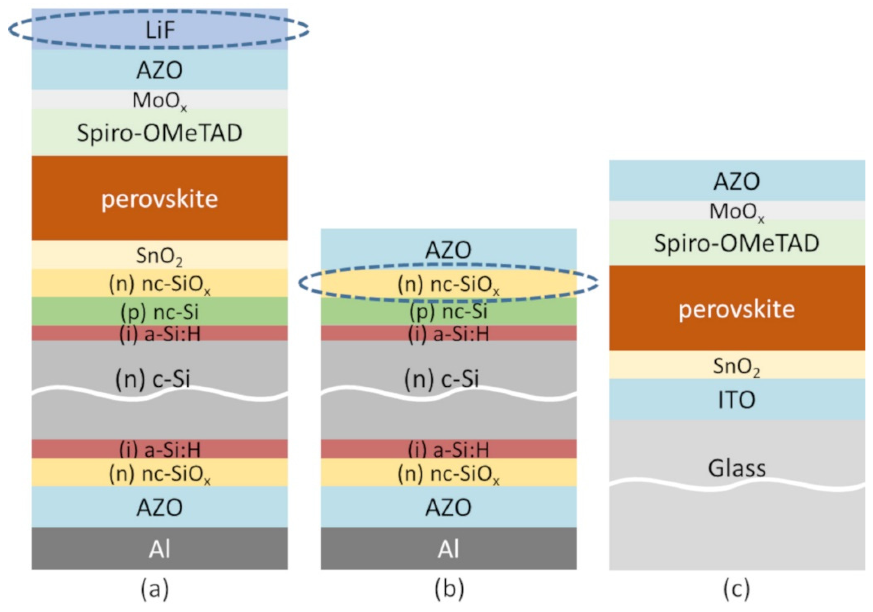
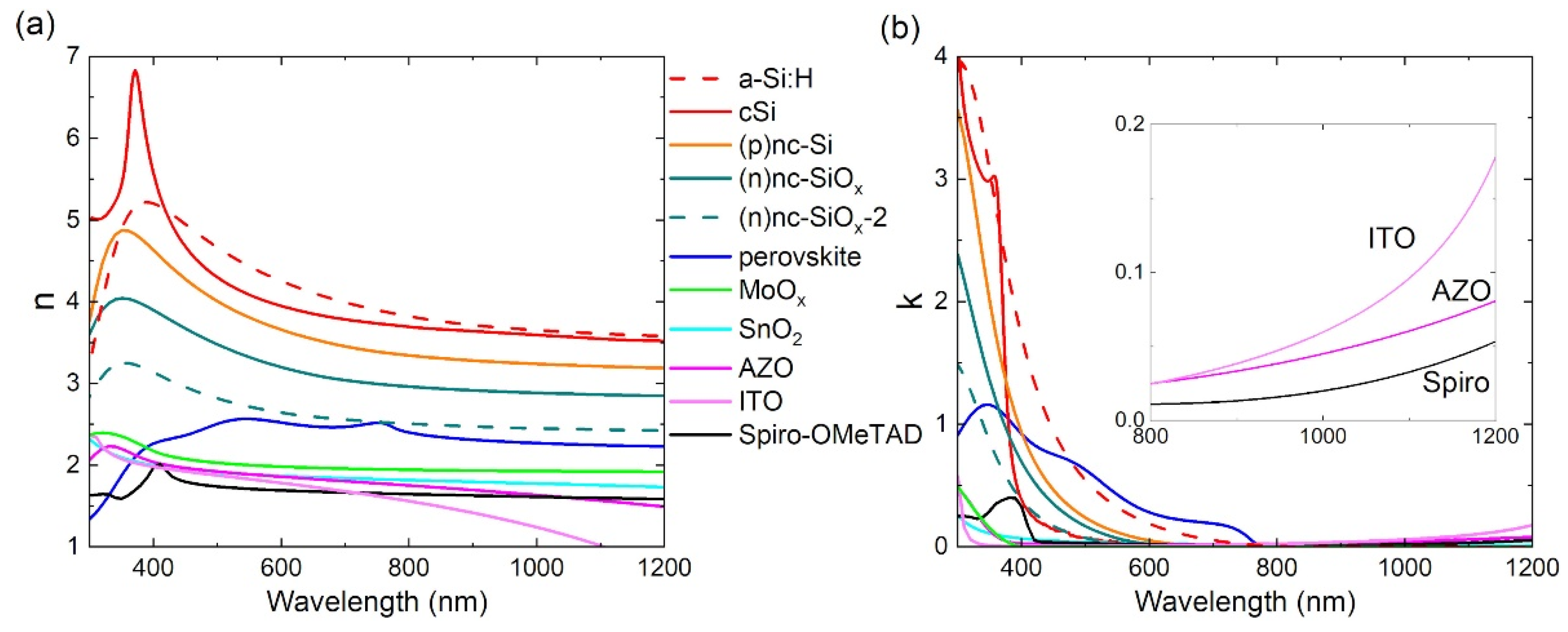
3.1. Device Design and Optical Simulations

We investigated a two-terminal monolithic tandem structure, where the two component cells are optically coupled and electrically connected in series. The structure is schematized in Figure 1a. The flat SHJ cell, with an additional interconnection layer, serves as the substrate for the deposition of the perovskite top cell. We selected a n-i-p top cell structure (deposition sequence of the layers), where the perovskite absorber is realized on top of a compact SnO2 layer (ETL) processed at low temperature to be compatible with the SHJ bottom cell. Accordingly, the n-type Si based SHJ bottom cell is prepared in the standard front emitter configuration, with the minority carrier (hole) collector (the (p)nc-Si layer) at the front side.
Along with the full tandem structure, we studied the main device components (SHJ bottom cell, tunnel junction, and semitransparent top cell) by fabricating and testing the devices illustrated in Figure 1b,c. In particular, we investigated SHJ solar cells with the additional (n)nc-SiOx layer applied for use as tunnel junction in combination with the underlying p-type layer versus the standard SHJ (solar cell structure with and without the layer circled with dashed line in Figure 1b). Semitransparent perovskite solar cells with the structure schematized in Figure 1c were also fabricated and tested.
The tandem solar cell presents a multilayer film over the flat silicon wafer and thus optical interference has a strong impact. To figure out the contribution and potential of the proposed tunnel junction, we performed a simple optical simulation study by using experimentally-determined complex refractive indices (n and k). All the layers were thus preliminarily characterized by spectroscopic ellipsometry. The spectra of the experimental optical constants are shown in Figure 2, together with literature data for c-Si [28]. The optical constants were obtained through simultaneous fitting of the multi-angle ellipsometry data and transmittance data with the J.A. Woollam WASE software using appropriate dispersion laws for each material. In particular, a-Si:H, (n)nc-SiOx, (p)nc-Si, MoOx, ITO, AZO, and SnO2 layers were described using the Tauc-Lorentz dispersion dependence, with the addition of the Drude model where needed to account for the free-carrier absorption contribution. Multiple Tauc-Lorentz oscillators were used for perovskite and Spiro-OMeTAD [29,30].
The materials span a wide range of refractive index values (Figure 2a), going from values below 2 at wavelengths around 800 nm for TCOs (AZO, ITO) and the contact/buffer layers of the top cell (SnO2, Spiro-OMeTAD, MoOx), to 2.4 for the perovskite absorber, to ~2.5 or ~3 for the silicon-rich (n)nc-SiOx films depending on the oxygen content (lower in the latter case), and finally to 3.3 for the (p)nc-Si film and 3.7–3.8 for c-Si and a-Si:H. From this synoptic view, it is evident that silicon-rich nc-SiOx can provide a suitable refractive index grading for the light traveling from the perovskite top cell to the c-Si bottom cell.
Figure 2b highlights the much larger extinction coefficient (and then absorption coefficient) for wavelengths above 400 nm and sharp absorption edge of the perovskite absorber versus indirect-bandgap crystalline silicon. In addition, information can be gathered on the parasitic absorption losses contributed by the various supportive layers. The silicon- and silicon oxide-based contact layers are characterized by large k at short wavelengths (decreasing with increasing oxygen content). However, the materials are applied as ultrathin layers (~20 nm) in the devices and, above all, this wavelength range is absorbed by the top cell and does not reach the layers. Relevant losses at short wavelengths are instead expected from the Spiro-OMeTAD layer (~150 nm thick, as evaluated for single layers on glass through ellipsometry), which is applied as window layer in the tandem configuration. Finally, TCOs and Spiro-OMeTAD contribute parasitic losses in the near-infrared range due to free carrier absorption (rising tails at long wavelengths in Figure 2b).
Based on the experimental optical constants of all the layers, we evaluated the internal transmittance into silicon within the tandem structure, i.e., the actual light that reaches the bottom absorber layer, for different configurations of the capping layers: thickness and material type in the tunnel junction, thickness of perovskite absorber, thickness of front Spiro-OMeTAD layer. For completeness, for the latter case (variation of Spiro-OMeTAD layer thickness) we evaluated also the internal transmittance into the perovskite absorber, i.e., the actual light that enters the top absorber layer. The simulations were carried out with the IMD software for optical modelling of multilayer films [31]. The modelled structures are: AZO/MoOx/Spiro-OMeTAD/(perovskite output medium) for the top cell, AZO/MoOx/Spiro-OMeTAD/perovskite/SnO2/tunnel-junction/a-Si:H/(c-Si output medium) for the bottom cell, with the selected absorber material (top or bottom) as output medium. The layer thicknesses were set to realistic values, based on estimations by means of optical characterization. In particular, unless the parameter was deliberately changed (see Figure 3 and values in the legends), we used 80 nm for AZO, 10 nm for MoOx, 150 nm for Spiro-OMeTAD, 400 nm for perovskite, 20 nm for SnO2, 30 nm for n-SiOx, 20 nm for (p)nc-Si, 5 nm for the a-Si:H passivation layer.
The simulated spectra are reported in Figure 3. Strong interference fringes dominate the transmittance spectra due to the flat interfaces. Figure 3a shows the effect of the n-type material in the tunnel junction on the light transmitted into silicon. Here four different materials are tested, with thickness fixed at 30 nm in all cases (for (n)nc-Si the same optical parameters as for (p)nc-Si have been used as a reasonable approximation). With ITO, the transmittance is shifted towards large wavelengths and is globally lower, because of the refractive index mismatch that causes back reflection of light. Using higher refractive index materials, such as silicon-rich (n)nc-SiOx (better with lower oxygen content) and (n)nc-Si, makes for increased light in-coupling into Si (increased T in Figure 3a) with potential increase of the current generated in the SHJ bottom cell. In Figure 3b, we can observe the effect of the n-layer thickness when using the proposed (n)nc-SiOx layer: with thicker layer the interference fringes are flattened, with impact on potential JSC values. The optical effects of the tunnel junction might however easily be masked by modifications in the interference pattern because of thickness variation of other layers. For example, Figure 3c,d shows the strong influence of Spiro-OMeTAD and perovskite layer thickness on the internal transmission into Si.

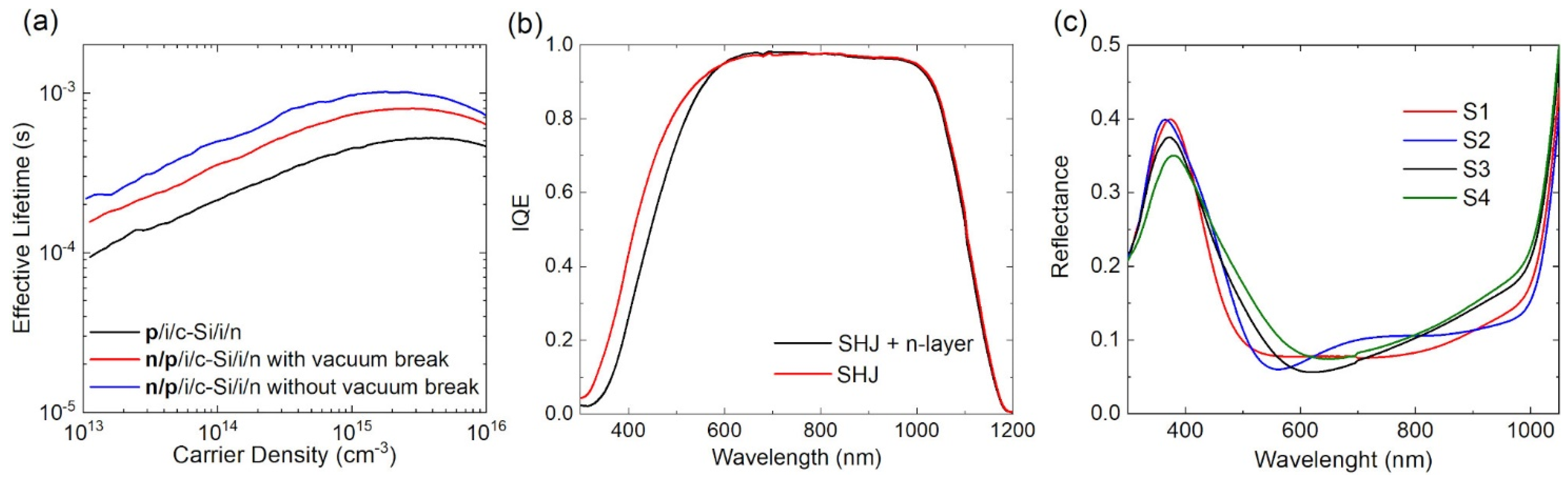
3.2. Tunnel Recombination Junction

We investigated SHJ solar cells with the architecture illustrated in Figure 1b. Each processed c-Si wafer was partially dedicated to the tunnel junction study, after being completed with front TCO and metal grid, and partially further processed to fabricate full tandem devices, for a direct comparison with a known bottom plus tunnel component.
Photoconductance decay measurements of SHJ solar cell precursors prior to the deposition of the electrodes showed a lifetime increase, and thus a potentially higher open circuit voltage, when applying the additional front n-type layer (red versus black curves in Figure 4a measured for the same sample before and after the n-layer deposition). This is likely due to the n-layer deposition process with high hydrogen dilution at 150 °C that may induce a hydrogen plus thermal treatment, resulting in improved chemical passivation of the wafer [26]. The lifetime is even larger if the additional n-layer is applied over the p-layer without breaking the vacuum (blue curve in Figure 4a, measured for a different but nominally identical sample fabricated without breaking the vacuum). On this basis, except for preliminary tests on SHJ cells with and without the additional n-layer, which require breaking the vacuum for cutting and removing part of the processed wafer from the PECVD reactor, we proceeded with modified SHJs that included the top n-layer with no vacuum break, to fully benefit from the lifetime improvement.
To check for possible optical losses, we measured and compared the internal quantum efficiency (IQE) of SHJ solar cells with and without the additional (n)nc-SiOx layer (Figure 4b). An obvious loss is present at short wavelength (not relevant in the tandem application where this portion of the light spectrum is absorbed by the top cell), due to parasitic absorption in the extra layer, while no impact is observed in the relevant long wavelength range.
Different tunnel junctions were tested, whose optical effect on the cell reflectance is shown in Figure 4c. Thicknesses around standard values for mixed-phase doped layers in SHJ solar cells were considered. A nominal thickness of 20 nm, based on the material deposition rate, was chosen for the p-type layer and target values between 15 nm and 60 nm were considered for the n-type layer (samples S1, S2, S3, respectively corresponding to middle, thick, and thin values). One additional configuration was considered with thicker p-type layer (sample S4, with nominal thickness of 30 nm). Table 1 reports the thicknesses of the p- and n-layers in the tunnel junction as obtained by fitting the experimental reflectance spectra with the IMD software based on the known optical constants (Section 3.1), showing a good agreement with the nominal set values.
The PV performance parameters of the devices are reported in the same table. The relevant parameters in this experiment are VOC and FF. SHJ solar cells with the additional n-layer are characterized by increased VOC, up to 711 mV, with respect to the reference cell without, thanks to the improved passivation discussed above. The FF stays above 70% with thicker n-layer and appears to decrease with decreasing n-layer thickness (down to 62.4% for 15 nm thick n-layer), because of a larger series resistance, possibly related to the reduced conductivity of the thinner n-layers. The measured series resistance values are in fact 2.5, 2.1, 5.6, and 4.4 Ω cm2, in this order for the devices S1, S2, S3, and S4.

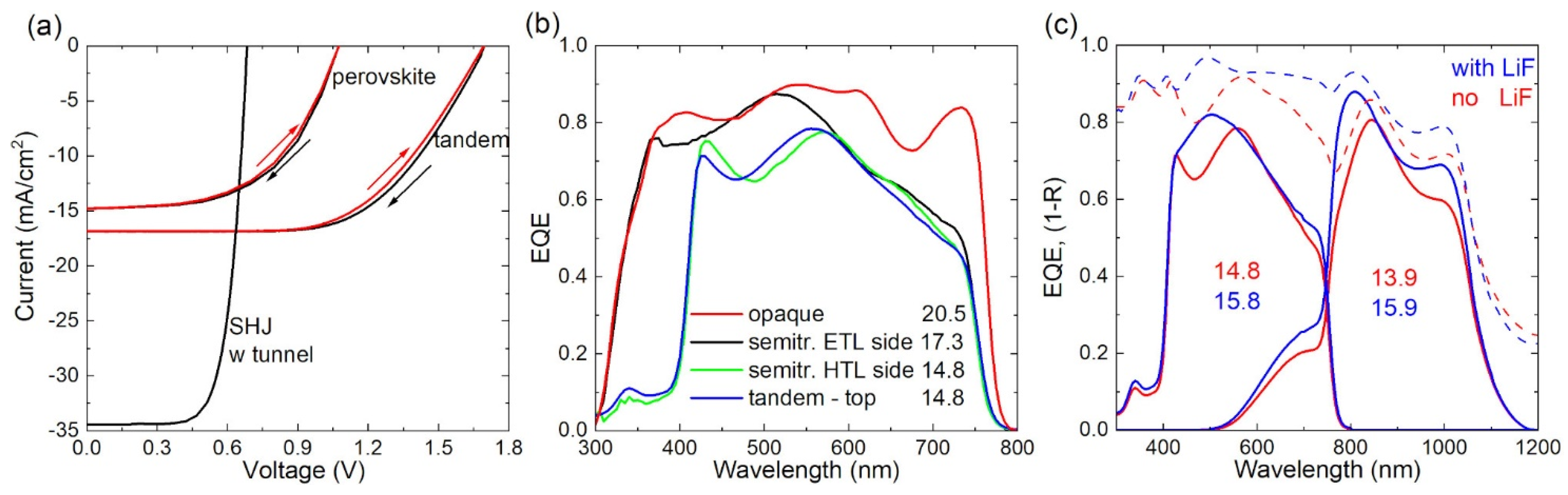
3.3. Semitransparent Perovskite Solar Cells and Perovskite/SHJ Tandem Solar Cells

A planar triple-cation perovskite sub-cell has been selected, with bandgap of the absorber evaluated as 1.64 eV from the inflection point of EQE spectra. The top component cell has been firstly tested as semitransparent single-junction device on glass/ITO (structure illustrated in Figure 1c). The metal electrode of standard opaque cells has been replaced with AZO and a thin buffer (10 nm) of evaporated MoOx has been included to protect the soft Spiro-OMeTAD layer and avoid losses from sputter damage during the AZO deposition, typically resulting in S-shaped J-V curves. The performance metrics of representative semitransparent and opaque solar cells (with Au electrode) are reported in Table 1. Here, the semitransparent cell is measured with light entering from the HTL side as in the tandem configuration. The hysteresis-free J-V curve of this cell is shown in Figure 5a. Against the opaque solar cell, the semitransparent device has lower FF (Table 1) due to high series resistance, at least partially related to a not optimized contact scheme. The EQEs of opaque and semitransparent cells are reported in Figure 5b together with the corresponding integrated JSC values. In the semitransparent case with illumination through the ETL, JSC is obviously reduced with respect to the opaque device due to the missing contribution from light reflected back into the perovskite absorber by the rear metal electrode. In addition, with illumination through the HTL, parasitic absorption into the Spiro-OMeTAD layer impacts the EQE at short wavelengths, whose shape agrees with the simulated internal transmittance into perovskite (dashed lines in Figure 3c).
Tandem solar cells with variable tunnel junction have been fabricated and characterized. Figure 5a shows the JV curves of a full tandem including the LiF antireflection layer (cell A in Table 1), together with the curves of the co-deposited bottom component cell and a reference semitransparent perovskite solar cell illuminated from HTL side as in the tandem configuration. The FF of 63.4% and the absence of S-shapes in the J-V curves evidence that the proposed tunnel junction is able to prevent the formation of parasitic junctions. In addition, the low lateral conductivity of the nanocrystalline layers might have contributed to achieve a high shunt resistance by mitigating possible shunt paths. The VOC of 1.660 V approaches the sum of the VOC values measured for the two subcells and, overall, the tandem cell shows an improved efficiency with respect to the reference single junction devices (cell A vs. S1 and Semitransp. Perovskite cell in Table 1). Moreover, as with the single-junction perovskite solar cells, the perovskite/SHJ tandem cells also show negligible J-V hysteresis (Figure 5a).
From the spectral response investigation, we can observe that the EQE of the top component cell replicates the curve measured for the single-junction cell (Figure 5b) with no impact from the different substrate, i.e., the SHJ bottom cell with tunnel junction vs. glass/ITO. As for the spectral sharing in the tandem, Figure 5c shows the EQE of top and bottom components prior and after the application of the LiF antireflection coating. The reflectance spectra of the tandem cell are also reported in the figure, shown as 1-R as a measure of the light absorbed by active and passive layers. As expected, the planar and non-scattering design of the tandem devices results in strong optical interferences, clearly identified in the EQE and reflectance spectra. In particular, the interference patterns observed in the measured EQE spectra qualitatively agree with the simulated internal transmittance into the absorber layers (Figure 3). Quantitatively, the EQE measurements show that prior to LiF application the device is bottom limited. With the application of the AR coating, a matched condition around 15.8 mA/cm2 is reached and the total JSC (sum of top and bottom contributions) increases from 28.7 mA/cm2 to 31.7 mA/cm2 thanks to the reduced reflection losses.
Finally, Figure 6 summarizes the effect of the changes in the tunnel junction on the tandem performance. Comparing the different bottom cell EQEs (Figure 6a) we can observe that, according to the simulated internal T in Figure 3b, the interference fringes are abated when thicker (n)nc-SiOx is applied. This is clear when comparing the spectra represented with solid lines in the figure, where the red curve corresponds to the cell with 55 nm thick layer and the black curve to the cell with 15 nm thick layer. When considering all the curves, the effect is partially masked by other contributions, like thickness variation of other layers affecting the pattern of spectral fringes, as observed in the simulation (Figure 3). The distribution of the electrical parameters, VOC and FF, is reported in Figure 6b,c for co-deposited tandem cells (cells fabricated over pieces cut from the same c-Si wafer for each tunnel junction configuration). As for FF, the values are generally around 60%, at least partially due to the not optimized front electrode. A trend appears for VOC, with larger values for the cells with thinner n-layer in the tunnel junction (Figure 6b). For the tunnel junction with only 15 nm thick n-layer, however there is more variability among the measured VOC values and, additionally, the JV curves are S-shaped, hence the low FF in Figure 6c. In this case also the bottom component itself has the lowest FF (Table 1). The most promising condition appears to be the tunnel junction with slightly thicker p-layer and ~20 nm thick n-layer, characterized by minor variability in VOC (Figure 6b) and no S-shape in the JV curve. The PV parameters of the best cell of this batch are reported in Table 1 as cell B. We point out that in this case the VOC of the tandem cell matches the sum of the VOC-s contributed by the two component cells, meaning negligible electrical losses at the tunnel junction.

4. Conclusions

We have investigated a p/n tunnel junction into monolithic perovskite/SHJ solar cells employing a Cs0.05FA0.8MA0.15PbI2.5Br0.5 perovskite top cell with n-i-p design, fabricated via solution processes at low temperature, and a SHJ bottom cell made from double-side polished n-type Si wafer. A nanocrystalline Si/SiOx based p/n structure is proposed, where the p-type layer ((p)nc-Si) also functions as selective contact layer for the SHJ bottom cell, while the n-type layer ((n)nc-SiOx), similarly deposited by PECVD as other functional layers of the bottom cell, provides suitable refractive index grading for the light passing from the perovskite top cell to the silicon bottom cell. Electrically, the (n)nc-SiOx layer can mitigate possible shunt paths in the devices. In addition, improved Si wafer passivation in the presence of the proposed bilayer has been observed, with consequent increased VOC of the bottom subcell. Different thicknesses of the n-type layer have been tested and the experimental study has been complemented with basic optical simulations as a guideline about effects on interference patterns. The results of the full tandem cells (1 cm2 area) prove the feasibility of the concept, with a VOC that appears to be larger with thinner n-layer in the tunnel junction. In particular, a value of ~1.8 V is reached, that equals the sum of the VOC-s of top and bottom components with no electrical losses contributed by the tunnel junction. We emphasize that, together with possible optical and electrical advantages, this approach provides for a simplification of the fabrication process and avoids the use of an ITO interlayer, thus tackling the issue of supply risk and high price of indium. This is a very relevant aspect considering that no solar PV technology that requires indium can be sustainably manufactured at scale [1].

Author Contributions

Conceptualization, L.V.M. and P.D.V.; formal analysis, L.V.M.; investigation, L.V.M., E.B., A.D.M., M.D.N., M.F., V.L.F., L.L., G.R., G.V.S. and I.U.; writing—original draft preparation, L.V.M.; writing—review and editing, all; project administration, P.D.V. All authors have read and agreed to the published version of the manuscript.

Funding

This work was supported by the Italian Ministry of Ecological Transition in the framework of the Operating Agreement with ENEA for Research on the Electric System.

Institutional Review Board Statement

Not applicable.

Informed Consent Statement

Not applicable.

Data Availability Statement

The data presented in this study are available on request from the corresponding author.

Conflicts of Interest

The authors declare no conflict of interest.

References

  1. Zhang, Y.; Kim, M.; Wang, L.; Verlinden, P.; Hallam, B. Design Considerations for Multi-Terawatt Scale Manufacturing of Existing and Future Photovoltaic Technologies: Challenges and Opportunities Related to Silver, Indium and Bismuth Consumption. Energy Environ. Sci. 2021, 14, 5587–5610. [Google Scholar] [CrossRef]
  2. Reyes-Belmonte, M.A. Quo Vadis Solar Energy Research? Appl. Sci. 2021, 11, 3015. [Google Scholar] [CrossRef]
  3. Almansouri, I.; Ho-Baillie, A.; Bremner, S.P.; Green, M.A. Supercharging Silicon Solar Cell Performance by Means of Multijunction Concept. IEEE J. Photovolt. 2015, 5, 968–976. [Google Scholar] [CrossRef]
  4. Green, M.A.; Dunlop, E.D.; Hohl-Ebinger, J.; Yoshita, M.; Kopidakis, N.; Hao, X. Solar Cell Efficiency Tables (Version 58). Prog. Photovolt. Res. Appl. 2021, 29, 657–667. [Google Scholar] [CrossRef]
  5. Al-Ashouri, A.; Köhnen, E.; Li, B.; Magomedov, A.; Hempel, H.; Caprioglio, P.; Márquez, J.A.; Vilches, A.B.M.; Kasparavicius, E.; Smith, J.A.; et al. Monolithic Perovskite/Silicon Tandem Solar Cell with >29% Efficiency by Enhanced Hole Extraction. Science 2020, 370, 1300–1309. [Google Scholar] [CrossRef] [PubMed]
  6. Jošt, M.; Kegelmann, L.; Korte, L.; Albrecht, S. Monolithic Perovskite Tandem Solar Cells: A Review of the Present Status and Advanced Characterization Methods Toward 30% Efficiency. Adv. Energy Mater. 2020, 10, 1904102. [Google Scholar] [CrossRef]
  7. Jeong, J.; Kim, M.; Seo, J.; Lu, H.; Ahlawat, P.; Mishra, A.; Yang, Y.; Hope, M.A.; Eickemeyer, F.T.; Kim, M.; et al. Pseudo-Halide Anion Engineering for α-FAPbI3 Perovskite Solar Cells. Nature 2021, 592, 381–385. [Google Scholar] [CrossRef]
  8. Hörantner, M.T.; Leijtens, T.; Ziffer, M.E.; Eperon, G.E.; Christoforo, M.G.; McGehee, M.D.; Snaith, H.J. The Potential of Multijunction Perovskite Solar Cells. ACS Energy Lett. 2017, 2, 2506–2513. [Google Scholar] [CrossRef]
  9. Sahli, F.; Kamino, B.A.; Werner, J.; Bräuninger, M.; Paviet-Salomon, B.; Barraud, L.; Monnard, R.; Seif, J.P.; Tomasi, A.; Jeangros, Q.; et al. Improved Optics in Monolithic Perovskite/Silicon Tandem Solar Cells with a Nanocrystalline Silicon Recombination Junction. Adv. Energy Mater. 2018, 8, 1701609. [Google Scholar] [CrossRef]
  10. Mazzarella, L.; Lin, Y.-H.; Kirner, S.; Morales-Vilches, A.B.; Korte, L.; Albrecht, S.; Crossland, E.; Stannowski, B.; Case, C.; Snaith, H.J.; et al. Infrared Light Management Using a Nanocrystalline Silicon Oxide Interlayer in Monolithic Perovskite/Silicon Heterojunction Tandem Solar Cells with Efficiency above 25%. Adv. Energy Mater. 2019, 9, 1803241. [Google Scholar] [CrossRef]
  11. Saliba, M.; Matsui, T.; Seo, J.-Y.; Domanski, K.; Correa-Baena, J.-P.; Nazeeruddin, M.K.; Zakeeruddin, S.M.; Tress, W.; Abate, A.; Hagfeldt, A.; et al. Cesium-Containing Triple Cation Perovskite Solar Cells: Improved Stability, Reproducibility and High Efficiency. Energy Environ. Sci. 2016, 9, 1989–1997. [Google Scholar] [CrossRef] [PubMed] [Green Version]
  12. Yoshikawa, K.; Kawasaki, H.; Yoshida, W.; Irie, T.; Konishi, K.; Nakano, K.; Uto, T.; Adachi, D.; Kanematsu, M.; Uzu, H.; et al. Silicon Heterojunction Solar Cell with Interdigitated Back Contacts for a Photoconversion Efficiency over 26%. Nat. Energy 2017, 2, 1–8. [Google Scholar] [CrossRef]
  13. Ru, X.; Qu, M.; Wang, J.; Ruan, T.; Yang, M.; Peng, F.; Long, W.; Zheng, K.; Yan, H.; Xu, X. 25.11% Efficiency Silicon Heterojunction Solar Cell with Low Deposition Rate Intrinsic Amorphous Silicon Buffer Layers. Sol. Energy Mater. Sol. Cells 2020, 215, 110643. [Google Scholar] [CrossRef]
  14. Liu, Y.; Li, Y.; Wu, Y.; Yang, G.; Mazzarella, L.; Procel-Moya, P.; Tamboli, A.C.; Weber, K.; Boccard, M.; Isabella, O.; et al. High-Efficiency Silicon Heterojunction Solar Cells: Materials, Devices and Applications. Mater. Sci. Eng. R Rep. 2020, 142, 100579. [Google Scholar] [CrossRef]
  15. Bastiani, M.D.; Subbiah, A.S.; Aydin, E.; Isikgor, F.H.; Allen, T.G.; Wolf, S.D. Recombination Junctions for Efficient Monolithic Perovskite-Based Tandem Solar Cells: Physical Principles, Properties, Processing and Prospects. Mater. Horiz. 2020, 7, 2791–2809. [Google Scholar] [CrossRef]
  16. Albrecht, S.; Saliba, M.; Baena, J.P.C.; Lang, F.; Kegelmann, L.; Mews, M.; Steier, L.; Abate, A.; Rappich, J.; Korte, L.; et al. Monolithic Perovskite/Silicon-Heterojunction Tandem Solar Cells Processed at Low Temperature. Energy Environ. Sci. 2016, 9, 81–88. [Google Scholar] [CrossRef]
  17. Bush, K.A.; Palmstrom, A.F.; Yu, Z.J.; Boccard, M.; Cheacharoen, R.; Mailoa, J.P.; McMeekin, D.P.; Hoye, R.L.Z.; Bailie, C.D.; Leijtens, T.; et al. 23.6%-Efficient Monolithic Perovskite/Silicon Tandem Solar Cells with Improved Stability. Nat. Energy 2017, 2, 1–7. [Google Scholar] [CrossRef]
  18. Aydin, E.; Liu, J.; Ugur, E.; Azmi, R.; Harrison, G.T.; Hou, Y.; Chen, B.; Zhumagali, S.; Bastiani, M.D.; Wang, M.; et al. Ligand-Bridged Charge Extraction and Enhanced Quantum Efficiency Enable Efficient n–i–p Perovskite/Silicon Tandem Solar Cells. Energy Environ. Sci. 2021, 14, 4377–4390. [Google Scholar] [CrossRef]
  19. Puaud, A.; Ozanne, A.-S.; Senaud, L.-L.; Muñoz, D.; Roux, C. Microcrystalline Silicon Tunnel Junction for Monolithic Tandem Solar Cells Using Silicon Heterojunction Technology. IEEE J. Photovolt. 2021, 11, 58–64. [Google Scholar] [CrossRef]
  20. Mercaldo, L.V.; Usatii, I.; Veneri, P.D. Advances in Thin-Film Si Solar Cells by Means of SiOx Alloys. Energies 2016, 9, 218. [Google Scholar] [CrossRef] [Green Version]
  21. Despeisse, M.; Bugnon, G.; Feltrin, A.; Stueckelberger, M.; Cuony, P.; Meillaud, F.; Billet, A.; Ballif, C. Resistive Interlayer for Improved Performance of Thin Film Silicon Solar Cells on Highly Textured Substrate. Appl. Phys. Lett. 2010, 96, 073507. [Google Scholar] [CrossRef]
  22. Čampa, A.; Meier, M.; Boccard, M.; Mercaldo, L.V.; Ghosh, M.; Zhang, C.; Merdzhanova, T.; Krč, J.; Haug, F.-J.; Topič, M. Micromorph Silicon Solar Cell Optical Performance: Influence of Intermediate Reflector and Front Electrode Surface Texture. Sol. Energy Mater. Sol. Cells 2014, 130, 401–409. [Google Scholar] [CrossRef]
  23. Jiang, Q.; Zhang, L.; Wang, H.; Yang, X.; Meng, J.; Liu, H.; Yin, Z.; Wu, J.; Zhang, X.; You, J. Enhanced Electron Extraction Using SnO2 for High-Efficiency Planar-Structure HC(NH2)2PbI3-Based Perovskite Solar Cells. Nat. Energy 2016, 2, 1–7. [Google Scholar] [CrossRef]
  24. Jeon, N.J.; Noh, J.H.; Kim, Y.C.; Yang, W.S.; Ryu, S.; Seok, S.I. Solvent Engineering for High-Performance Inorganic–Organic Hybrid Perovskite Solar Cells. Nat. Mater. 2014, 13, 897–903. [Google Scholar] [CrossRef]
  25. La Ferrara, V.; De Maria, A.; Rametta, G.; Delli Veneri, P. The Effect of Storage Cycle on Improvement in the Photovoltaic Parameters of Planar Triple Cation Perovskite Solar Cells. Mater. Adv. 2021, 2, 5396–5405. [Google Scholar] [CrossRef]
  26. Mercaldo, L.V.; Bobeico, E.; Usatii, I.; Della Noce, M.; Lancellotti, L.; Serenelli, L.; Izzi, M.; Tucci, M.; Delli Veneri, P. Potentials of Mixed-Phase Doped Layers in p-Type Si Heterojunction Solar Cells with ZnO:Al. Sol. Energy Mater. Sol. Cells 2017, 169, 113–121. [Google Scholar] [CrossRef]
  27. Demaurex, B.; De Wolf, S.; Descoeudres, A.; Charles Holman, Z.; Ballif, C. Damage at Hydrogenated Amorphous/Crystalline Silicon Interfaces by Indium Tin Oxide Overlayer Sputtering. Appl. Phys. Lett. 2012, 101, 171604. [Google Scholar] [CrossRef] [Green Version]
  28. Palik, E.D. (Ed.) Handbook of Optical Constants of Solids; Academic Press: Boston, MA, USA, 1998; ISBN 978-0-12-544422-4. [Google Scholar]
  29. Raoult, E.; Bodeux, R.; Jutteau, S.; Rives, S.; Yaiche, A.; Coutancier, D.; Rousset, J.; Collin, S. Optical Characterizations and Modelling of Semitransparent Perovskite Solar Cells for Tandem Applications. Eur. Photovolt. Sol. Energy Conf. Exhib. 2019, 757–763. [Google Scholar] [CrossRef]
  30. Shirayama, M.; Kadowaki, H.; Miyadera, T.; Sugita, T.; Tamakoshi, M.; Kato, M.; Fujiseki, T.; Murata, D.; Hara, S.; Murakami, T.N.; et al. Optical Transitions in Hybrid Perovskite Solar Cells: Ellipsometry, Density Functional Theory, and Quantum Efficiency Analyses for CH3NH3PbI3. Phys. Rev. Appl. 2016, 5, 014012. [Google Scholar] [CrossRef] [Green Version]
  31. IMD Can Be Run as an Extension to the Free XOP Software Package, Available at ESRF. Available online: Esrf.fr/Instrumentation/software/data-analysis/xop2.4 (accessed on 19 October 2021).
Figure 1. Layout of the devices tested in this work (not in scale and front metal grid not drawn): (a) monolithic perovskite/SHJ tandem cell with and without LiF antireflection coating (circled layer); (b) SHJ solar cell, with and without the extra top n-type layer for tunnel junction testing (circled layer); (c) semi-transparent perovskite solar cell on glass/ITO.
Energies 14 07684 g001
Figure 2. Spectra of the optical constants of all the layers used in the devices, as obtained by spectroscopic ellipsometry plus c-Si from ref. [28]: (a) refractive index and (b) extinction coefficient with zoomed long wavelength range for ITO, AZO, and Spiro-OMeTAD shown in the inset. The (n)nc-SiOx-2 material is a possible alternative layer with higher oxygen content than the (n)nc-SiOx film used in the present devices.
Energies 14 07684 g002
Figure 3. Simulated internal transmittance into silicon in tandem solar cells in four cases: (a) different tunnel junction material applied over the (p)nc-Si layer, (b) variable (n)nc-SiOx layer thickness in the p/n tunnel junction, (c) different Spiro-OMeTAD thickness (in this case the internal transmittance into perovskite is also shown), (d) variable thickness of perovskite absorber.
Energies 14 07684 g003
Figure 4. Tunnel junction investigation: (a) effective lifetime of SHJ cell precursors, (b) IQE of SHJ solar cells with and without the additional top n-layer, (c) reflectance of SHJ solar cells with different top p/n tunnel junction (see Table 1 for correspondence of sample names and p/n layer thicknesses).
Energies 14 07684 g004
Figure 5. Tandem solar cells results: (a) J-V curves of full tandem with LiF and single-junction cells, (b) comparison of EQEs of perovskite solar cells with different design, (c) EQEs (solid lines) of top and bottom components of a tandem solar cell prior and after LiF coating together with the cell reflectance, reported as 1-R (dashed lines).
Energies 14 07684 g005
Figure 6. Tunnel junction effects on 1 cm2 tandem solar cells from co-deposited batches: EQE spectra of the bottom cells (a); distribution of VOC (b) and FF (c) data and median lines.
Energies 14 07684 g006
Table 1. Representative solar cells of each type: PV performance parameters, cell area, and actual thickness values of the tunnel junction as evaluated from cell reflectance spectra. For perovskite and tandem cells, PV parameters obtained from reverse scans are reported (data acquisition from high to low voltage).
CellVOC
(V)
JSC
(mA/cm2)
FF
(%)
η
(%)
Area
(cm2)
p/n
(nm/nm)
SHJ
S1-ref0.64134.671.515.8419/--
SHJ with tunnel junction
S10.68434.471.116.7419/37
S20.68033.272.116.2422/55
S30.71134.062.415.1421/15
S40.70233.366.415.5431/19
Perovskite
Opaque1.04520.579.217.00.11--/--
Semitransp.1.08214.855.18.80.63--/--
Tandem
A 11.66016.863.417.7119/37
B1.79512.871.516.5131/19
1 Tandem solar cell completed with antireflection coating (100 nm-thick LiF external layer).
Publisher’s Note: MDPI stays neutral with regard to jurisdictional claims in published maps and institutional affiliations.

