Article

Analysis and Output Power Control of Unidirectional Secondary-Resonant Single-Active-Half-Bridge DC-DC Converter

Electrical and Mechanical Engineering Department, Nagoya Institute of Technology, Gokiso-cho, Showa-ku, Nagoya 466-8555, Japan
*
Author to whom correspondence should be addressed.
Energies 2021, 14(21), 7432; https://doi.org/10.3390/en14217432
Submission received: 6 October 2021 / Revised: 30 October 2021 / Accepted: 2 November 2021 / Published: 8 November 2021
(This article belongs to the Special Issue DC-DC Converters Technologies, Applications and Optimization)

Abstract

:
Development of high-frequency-isolated DC-DC converters is underway for charging and discharging electric vehicle batteries. As a charger, a Single Active Bridge (SAB) converter, which is composed of a primary full-bridge converter, a high-frequency transformer, and a secondary full-bridge diode rectifier circuit, has been proposed as a unidirectional high frequency isolated DC-DC converter. In this paper, as a simple circuit configuration, a Secondary-Resonant Single-Active-Half-Bridge (SR-SAHB) converter, in which the primary and secondary circuits of the SAB converter are both half-bridge circuits, and a resonant capacitor connected in parallel to each secondary diode, is created. Due to the partial resonance on the secondary side, power transmission with unity transformer turn ratio and unity voltage conversion ratio can be realized, and a high total input power factor of the transformer can be achieved. As a result, the maximum voltage and current of the switching devices and the transformer voltage can be reduced. Moreover, soft switching in all commutations can be realized. The operation waveform is analyzed, and output power control is derived using the variable frequency control method. The effectiveness of the proposed SR-SAHB has been verified by experimental results using a 2.4 kW 20 kHz, 265 V laboratory prototype.

1. Introduction

Development of high-frequency-isolated DC-DC converters is underway for charging and discharging electric vehicle batteries. For bidirectional DC-DC converters, a dual-active-bridge (DAB) converter, in which the primary and secondary single-phase full-bridge converters are connected to a high-frequency transformer, has been proposed [1], and the range of soft switching has been clarified [2]. In the DAB converter, the output power can be easily controlled by the phase difference between the primary and secondary voltages. Further, unity voltage conversion ratio can be realized under the condition of unity transformer turn ratio, and a high total input power factor on the primary side of the transformer can be achieved. Therefore, the DAB converter is widely used as a compact and highly efficient converter [3].
A DC-DC converter using a half-bridge in the primary or secondary converters has also been proposed as a simple circuit configuration for a DAB converter [4,5,6]. The similar control and characteristics, which are same as the full-bridge DAB converter, can be realized with the half-bridge DAB converter. It has also been proposed in order to employ the half-bridge DAB converter as the power controller among three-ports [7], and to expand the control range of soft switching by configuring the primary half-bridge in two parallel configurations [8].
For power application that is employed only for charging the battery, a unidirectional high-frequency isolated converter is used. As a unidirectional converter, a circuit in which the two switches on the secondary side of the DAB converter are replaced with diodes has been proposed. The control method for the output power from the rated load to the light load [9] and the control method according to the change of the voltage conversion ratio [10] are described.
A unidirectional converter, in which the full-bridge circuit of the secondary converter is replaced with a diode rectifier circuit and a reactor is installed in series between the diode rectifier circuit and the output smoothing capacitor, has been proposed. This circuit can realize unity voltage conversion ratio due to the current continuity of the reactor, and can also increase the total input power factor on the primary side of the transformer. High voltage diodes must be used due to the surge voltage generated by the reactor and the parasitic capacitors of the rectifier diode. Circuit configurations with an auxiliary circuit for suppressing the surge voltage have also been proposed [11,12].
An LLC converter has been proposed in which the full-bridge circuit of the secondary converter is replaced with a diode rectifier circuit, and a capacitor is installed in series with the transformer/leakage inductor in the primary circuit. A simpler topology for the LLC converter is the half-bridge configuration [13]. In the LCC converters, the sinusoidal current waveform of the transformer is obtained, and the soft switching is achieved by the primary series resonant circuit between the installed capacitor and the leakage inductance. Therefore, the transformer frequency is chosen to be close to the resonant frequency. For the control of the output voltage and current, a dual half-bridge LLC resonant converter with magnetic control has been proposed [14].
A single active bridge (SAB) converter has been proposed, in which the secondary converter is replaced with a diode full-bridge rectifier circuit, and a smoothing capacitor is directly connected to the rectifier circuit. High-efficiency experimental results using SiC have been obtained [15]. A comparison of soft switching capabilities between SAB and DAB converters has been clarified [16]. A method of reducing the loss by connecting a capacitor in parallel with the primary switch has also been proposed [17].
In the configuration of the SAB converter, the operating waveforms are compared, including a simpler circuit in which one or both of the primary converter and the secondary diode rectifier are replaced with a half bridge [18]. With the configuration of the primary full-bridge converter and the secondary half-bridge rectifier, the output DC voltage can be controlled to twice that of the input voltage [19]. Detailed waveform analysis and the response for the load change are clarified for a circuit with the primary half-bridge converter and the secondary full-bridge rectifier [20]. Furthermore, an application circuit that can expand the operating range of soft switching, and reduce the current ripple by using two parallel primary half-bridges and phase-shift control is also proposed [21].
In the SAB converter, under the conditions of unity transformer turn ratio and unity voltage conversion ratio, power cannot be sent since the secondary peak voltage of the transformer is equal to the output DC voltage, and the diode does not turn on. As the voltage conversion ratio of the SAB converter is designed as less than one, the total power factor of the high-frequency transformer is low [1]. Since the primary voltage and peak current are high values, the high-voltage and high-current switching devices and the high-voltage transformer are then required.
The authors realized the unity voltage conversion ratio for the full-bridge configuration of the SAB converter, and improved the total power factor of the high-frequency transformer by connecting a resonant capacitor in parallel to each of the secondary diode to configure a series LC resonant circuit on the secondary side. As a result, the maximum voltage and current of the switching devices and the transformer voltage can be reduced, and high efficiency is obtained [22]. Furthermore, the output power control has been proposed [23].
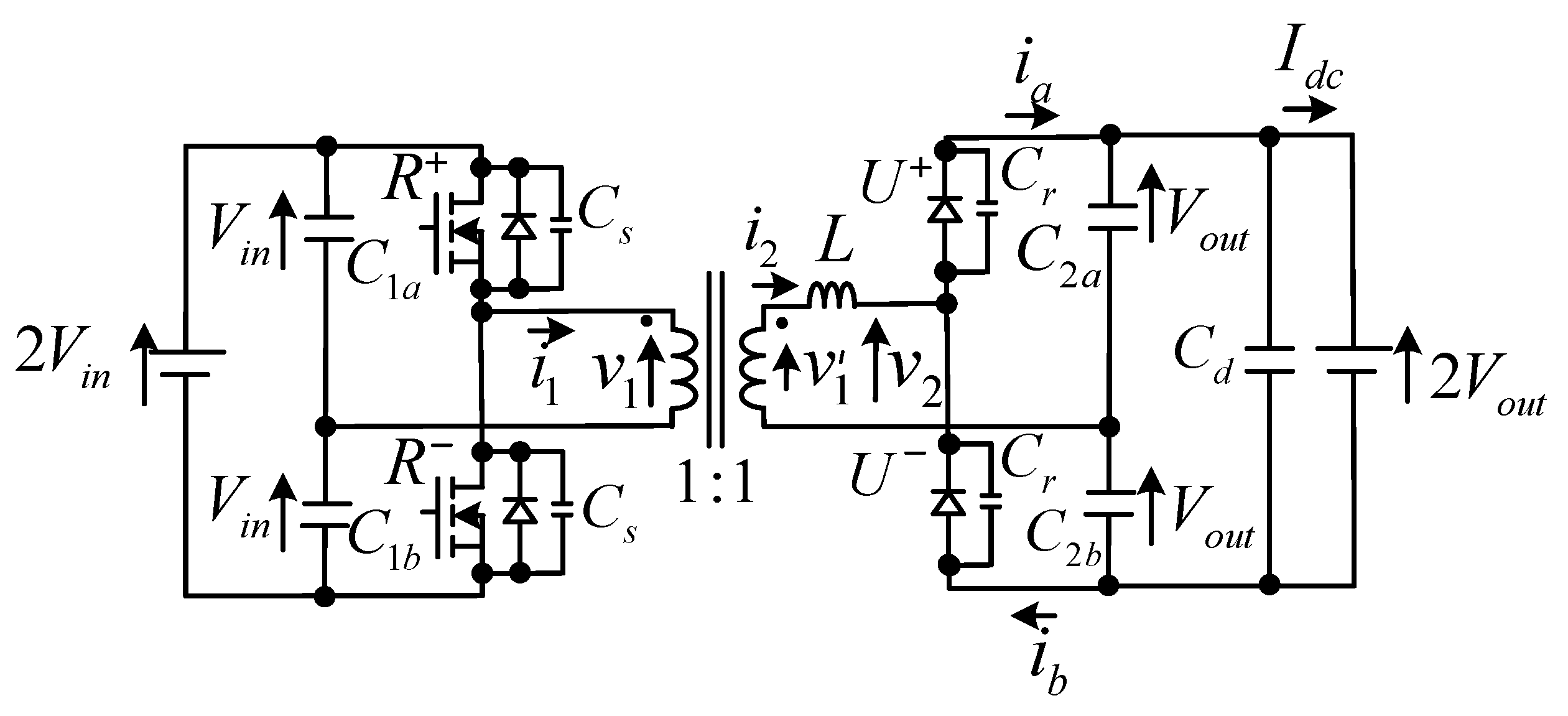
This paper presents a secondary resonant single-active half-bridge (SR-SAHB) DC-DC converter in which both the primary and secondary circuits are in the half-bridge configurations of the SAB converter with the secondary resonant circuit, as shown in Figure 1. Since the partial resonance occurs at the commutations of the secondary diodes, the resonant frequency is designed much higher than the rated transformer frequency. The proposed SR-SAHB converter can also realize soft switching in the primary and secondary circuits, unity voltage conversion ratio, and high total power factor of the high-frequency transformer. As a result, the maximum voltage and current of the switching devices and the transformer voltage can be reduced. The analysis of the operation waveform and circuit design method are derived. Furthermore, the output power control by changing the transformer frequency is proposed. The effectiveness of the proposed SR-SAHB converter has been verified by experimental results, using a using a 2.45 kW, 20 kHz rating laboratory prototype.

2. Conventional Single-Active-Half-Bridge Dc-Dc Converter

Figure 2a shows the configuration of a conventional unidirectional SAHB DC-DC converter. The SAHB converter is composed of a primary half-bridge converter, a high-frequency transformer, and a secondary diode half-bridge rectifier circuit. The input voltage 2 V i n is equally divided into two voltages of V i n by the series two capacitors C 1 a and C 1 b   ( C 1 a = C 1 b ) . The primary half-bridge converter is composed of two switches, R + and R , with the parasitic capacitance C s in parallel. The output voltage 2 V o u t is also equally divided into two voltages of V o u t by the series two capacitors C 2 a and C 2 b   ( C 2 a = C 2 b ) . The primary side terminals of the high-frequency transformer T r with the leakage inductance L connected to the output terminal of the primary half-bridge converter and neutral point of the input capacitors. The secondary side terminals of the transformer T r are connected to the input terminal of the secondary half-bridge rectifier of the diodes U + , U , and the neutral point of the output capacitors. The turn ratio of the transformer is expressed as a = N 1 / N 2 , using the primary and secondary numbers of turns N 1 and N 2 .
Figure 2b shows the secondary equivalent circuit of the conventional SAHB converter. The primary voltage component v 1 = v 1 / a , which is transformed from the primary voltage v 1 to the secondary side, is represented as the voltage across the secondary magnetizing inductance of the transformer. The leakage inductance L is presented as the equivalent value converted to the secondary side.
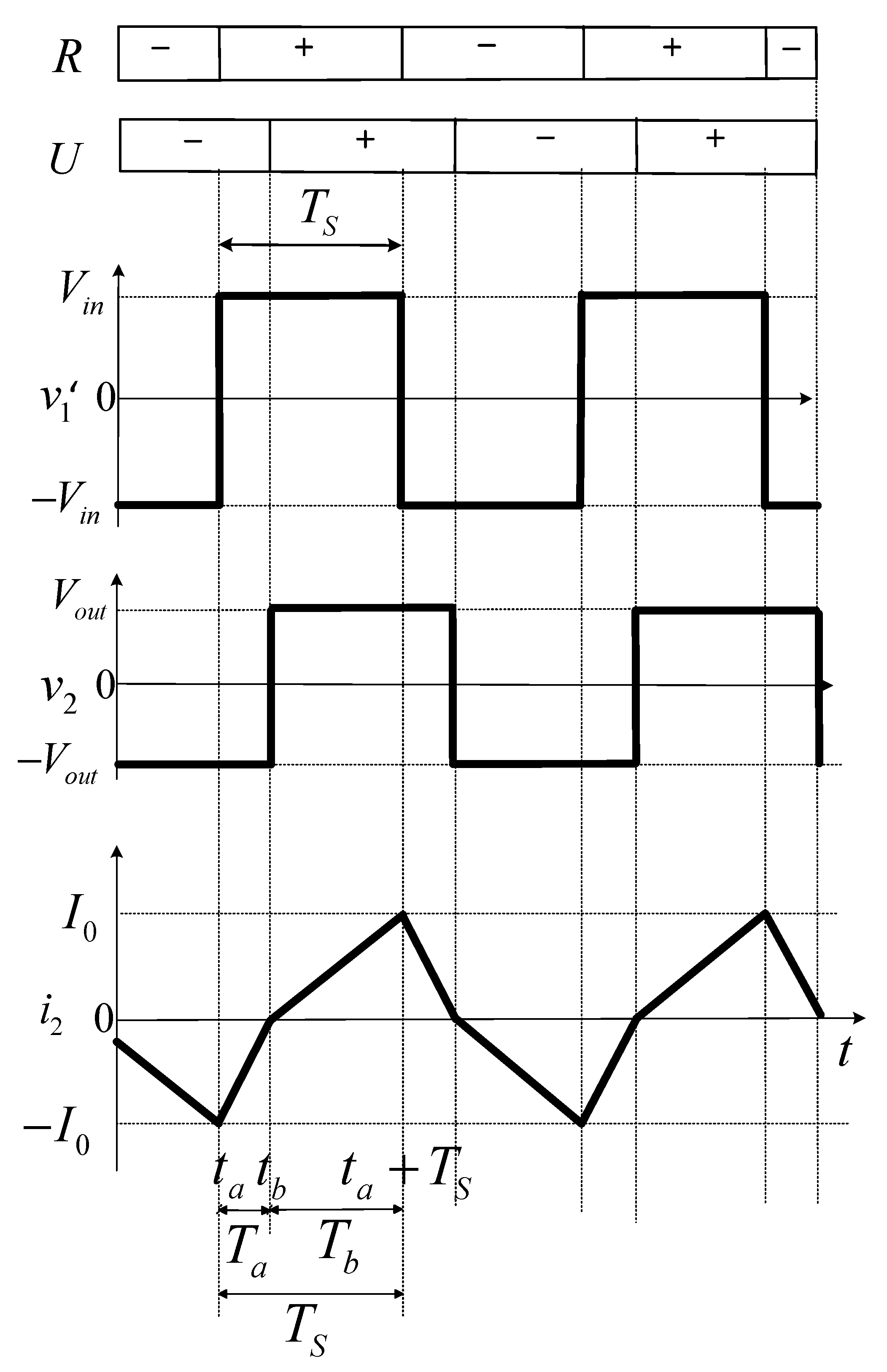
Figure 3 shows the voltage and current waveforms of the transformer in the steady state of the conventional SAHB converter. The waveforms are calculated under the conditions of unity turn ratio a = 1 , the constant voltages of the capacitors C 1 a , C 1 b , C 2 a , and C 2 b , and the zero-magnetizing current of the transformer. The primary voltages of the capacitors C 1 a and C 1 b are V i n , and the secondary voltages of the capacitors C 2 a and C 2 b are V o u t . The primary half-bridge converter generates a rectangular AC voltage v 1 = v 1 with the amplitude V i n and frequency f s ( = 1 / 2 T s )   by controlling switches R + and R with a 50 percent duty cycle. If the amplitude V i n of the primary voltage v 1 is equal to the output DC voltage V o u t in Figure 2b, the secondary diodes U + and U cannot be turned on, and no power is sent to the secondary side in the conventional converter. Therefore, the conventional converter does not work at the unity DC voltage conversion ratio M v = V o u t / V i n = 1 . In the voltage waveforms in Figure 3, the amplitude V i n of the primary voltage v 1 should be higher than the amplitude V o u t of the secondary voltage v 2 for sending power. Thus, the transformer currents i 1 and i 2 flow by the voltage difference between the primary voltage v 1 and the secondary voltage v 2 .
When the rectangular AC voltage v 1 = v 1 with the amplitude V i n is generated, the analytical transformer current i 2 is derived. The following secondary voltage equation of the transformer in Figure 2b is obtained:
v 1 = L d i 2 d t + v 2
The primary voltage v 1 = V i n is given by the turn-on of switch R + at the time t = t a in Figure 3. Since the secondary current i 2 is negative, the secondary diode U is kept in the “on” state and the secondary voltage v 2 = V o u t is generated. In Equation 1 , the primary voltage v 1 = V i n , the secondary voltage v 2 = V o u t , and the current i 2 t a = I o at t = t a are given; the secondary current i 2 t in the duration T a   t a t t b is calculated by the following equation:
i 2 t = V i n + V o u t L t t a I o   t a t t b
The duration T a is obtained in Equation (3) by using the relation of the secondary current i 2 t b = 0 in Equation (2):
T a = t b t a = L I o V i n + V o u t
After the secondary current i 2 t becomes zero at the time t = t b , the positive transformer current i 2 flows due to the positive primary voltage v 1 = V i n and the turn-on of the secondary diode U + . Since the primary voltage v 1 = V i n and the secondary voltage v 2 = V o u t in 1 are expressed, the secondary current i 2 t during the duration T b   t b t t a + T s is calculated by the following equation:
i 2 t = V i n V o u t L t t b t b t t a + T S
The duration T b is obtained using the half period T s = T a + T b and the duration T a in Equation (3) by the following equation:
T b = T s T a = T s L   I o V i n + V o u t
The peak current I o is calculated in Equation (6) since the secondary current i 2 t a + T s = I o at the time t = t a + T s = t b + T b in Equation (4):
i 2 t b + T b   = V i n V o u t L T s L I o V i n + V o u t = I o I o = V i n 2 V o u t 2 2 L V i n T s
Substituting I o in Equation (6) into Equations (3) and (5), the durations T a and T b are obtained in Equations (7) and (8), respectively:
T a = V i n V o u t 2 V i n T s
T b = V i n + V o u t 2 V i n T s
The output power P o u t is calculated from the secondary voltage v 2 = V o u t and current i 2 t during the half period duration t b t t b + T S by Equation (9):
P o u t = 1 T s t b t b + T s V o u t i 2 d t = V i n 2 V o u t 2 V o u t T s 4 L V i n
The effective value of the primary current I 1 is obtained as follows:
I 1 = 1 3 I o = 1 3 V i n 2 V o u t 2 2 L V i n T s
The primary total power factor T P F of the transformer is calculated in Equation (11) by substituting the output power P o u t in Equation (9), and the effective values of voltage V 1 = V i n and current I 1 in Equation (10):
T P F = P o u t V 1 I 1 = 3 V o u t 2 V i n
Table 1 shows a design example of the conventional SAHB and proposed SR-SAHB converters. Table 1A indicates the specifications of the converter of P o u t = 2.45   kW , 2 V o u t = 265   V , and f s = 20   kHz . Table 1B shows the designed parameters of the conventional SAHB and proposed SR-SAHB converters. The designed parameters of the conventional SAHB converter are the input DC voltage 2 V i n = 362   V , the voltage conversion ratio M v = 2 V o u t / 2 V i n = 0.73 , the peak current I o = 37   A , and the total power factor T P F = 0.63 . Although the designed parameters of the proposed SR-SAHB converter in Table 1B are derived in Section 4, the designed parameters of the proposed SR-SAHB converter have been greatly improved compared with those of the conventional SAHB converter. The input DC voltage 2 V i n is reduced by 27% from 362 V to 265 V, and the primary peak current is also reduced by 37% from I o = 37   A to I n = 23.3   A . The low-voltage and -current switching device can be selected in the proposed converter. The primary transformer voltage v 1 = V i n is also reduced by 27%. The small core size for the high-frequency transformer can be selected in the proposed converter.

3. Proposed Secondary-Resonant Single-Active-Half-Bridge DC-DC Converter

3.1. Circuit Configuration and Operating Waveforms

The feature of the proposed unidirectional SR-SAHB DC-DC converter configuration in Figure 1 is the resonant capacitors C r , which are connected to the secondary diodes U + and U in parallel to the conventional converter in Figure 2. The series resonance of the resonant capacitors C r and the leakage inductance L improves the voltage conversion ratio M v , and the total power factor T P F of the high-frequency transformer.
Figure 4 shows the operating waveforms in the proposed SR-SAHB converter under the conditions of the unity turn ratio of the high-frequency transformer a = 1 , the constant voltages of the capacitors C 1 a , C 1 b , C 2 a , and C 2 b , and the zero-magnetizing current of the high-frequency transformer. The SR-SAHB converter achieves the unity voltage conversion ratio   M v = 1   2 V i n = 2 V o u t . In Figure 4, the primary half-bridge converter generates the rectangular AC voltage v 1 = v 1 , with the amplitude V i n   = V o u t and frequency f s ( = 1 / 2 T s ) , by controlling switches R + and R with a 50 percent duty cycle. The secondary rectangular voltage v 2 with the amplitude V o u t is also generated. The secondary voltage v 2 is lagged when compared with the primary voltage v 1 . The primary and secondary currents i 1 and i 2 of the trapezoidal waveforms are obtained. The secondary currents i 2 is rectified by the secondary diode half-bridge rectifier, and the rectified currents i a and i b flow in the secondary circuit.

3.2. Soft-Switching Commutation of Primary Half-Bridge Converter

In the commutations between switches R + and R of the primary converter, soft switching is achieved. Figure 5 shows the soft-switching modes of the primary half-bridge converter from switch R to switch   R + .
In Mode 1–1 of Figure 5, switch R is conducting and the primary voltage v 1 of V i n is given. The primary current i 1 of negative value I n flows though the capacitor   C 1 b , transformer, and switch   R . The voltages of the parasitic capacitances C s of switches R and R + are zero and 2 V i n , respectively.
Mode 1–2 in Figure 5 begins when switch R turns off. At the time, the zero-voltage switching of switch R is achieved as the voltage of the parallel parasitic capacitances C s is zero. The primary current i 1 of negative value I n flows through the two parasitic capacitances C s . The capacitor voltages of switch R increases from zero to 2 V i n , and the capacitor voltages of switch R + decreases from 2 V i n to zero. As the parasitic capacitor voltages change, the primary voltage v 1 of the transformer changes from V i n to V i n .
Mode 1–3 in Figure 5 starts when the capacitor voltage of switch R + reaches zero and the parallel diode of switch R + is turned on. The primary current i 1 increases toward zero. Before the primary current i 1 reaches zero, the gate signals to turn on switch R + is given.
Mode 1–4 in Figure 5 starts when the sign of the primary current i 1 changes to positive, and switch R + is turned on. Since the voltages of switch R + and the parallel parasitic capacitances C s are kept to zero, zero-voltage switching is achieved.

3.3. Operating Analysis of Secondary Diode Rectifier Circuit

Figure 6 shows the commutation modes from diode U to diode U + of the secondary diode half-bridge rectifier circuit in the proposed SR-SAHB converter under the unity conversion ratio   M v = 1   2 V i n = 2 V o u t .
In Mode 2–1, the primary voltage v 1 = V 1 / a of V i n = V o u t is given, and the secondary current i 2 of negative value I n charges the capacitor C 2 b through diode U . The rectified current i b is the negative secondary current i 2 = I n . The parallel capacitor voltage of diode U is zero, and the parallel capacitor voltage of diode U + is charged to the output voltage 2 V o u t . When the primary voltage v 1   is changed from V i n to V i n = V o u t at t = t 2 , the operation of the circuit changes to Mode 2–2.
In Mode 2–2 during the duration t 2 t t 3 , diodes U remains in the “on” state, and the negative secondary current i 2 increases to zero due to the positive primary voltage v 1 = V i n = V o u t . The rectified current i b is the negative secondary current i 2 . When the secondary current i 2 reaches to zero at t = t 3 , diode U turns off at zero voltage, and the circuit becomes Mode 2–3.
In Mode 2–3 during the duration t 3 t t 4 , partial resonance occurs for the commutation from diode U to diode U + . At t = t 3 , the parallel capacitor voltage of diode U is zero, and the parallel capacitor voltage of diode U + is charged to the output voltage   2 V o u t . The resonance between inductor L and the two capacitors C r occurs. The sinusoidal secondary current i 2 is obtained. Since half of the secondary current i 2 / 2   flows through each capacitor C r owing to the circuit symmetry property, the rectified currents i a = i 2 / 2 and i b = i 2 / 2 flow. When the parallel capacitor voltages of diode U + and U become zero and 2 V o u t at t = t 4 , respectively, diode U + turns on at zero voltage, and the circuit becomes Mode 2–4. The primary and secondary voltages and currents in Mode 2–4 are the opposite signs of those in Mode 2–1.
The equations of the waveforms during the half period T S between Mode 2–3 and Mode 2–5 are derived. In the proposed SR-SAHB converter in Figure 1, the voltage Equation in Equation (1) holds.
In Mode 2–3, the following voltage equation is given by substituting the parallel capacitor voltage across diode U + and the voltage V o u t across the capacitor C 2 a into the secondary voltage v 2 in Equation (1).
v 1 = L d i 2 d t + 1 C r t 3 t i 2 2 d t V o u t
Substituting v 1 = V o u t and i 2 t 3 = 0 into Equation (12), the secondary current i 2 t in the duration t 3 t t 4 of Mode 2–3 is obtained as follows:
i 2 t = 2 V o u t 2 C r L sin t t 3 2 L C r     t 3 t t 4
The secondary voltage v 2 is obtained using the secondary current i 2 t in Equation (13) as follows:
v 2 t = v 1 t L d i 2 d t = V o u t 1 2 cos t t 3 2 L C r
The secondary current i 2 and voltage v 2   in Equations (13) and (14) are sinusoidal waveforms, as shown in Figure 4. Since diode U + turns on when the secondary voltage v 2 t   reaches V o u t at t = t 4 , Mode 2–3 is completed. The duration T 3 in Mode 2–3 and the amplitude I n of the secondary current i 2 t 4 are obtained from Equations (13) and (14) by the following equations:
T 3 = t 4 t 3 = π 2 2 L C r
I n = i 2 t 4 = 2 V o u t 2 C r L
The rectified currents i a = i 2 / 2 and i b = i 2 / 2 in Mode 2–3 are obtained as follows:
i a t   = i 2 t 2 = V o u t 2 C r L sin t t 3 2 L C r
i b t = i 2 t 2 = V o u t 2 C r L sin t t 3 2 L C r
In Mode 2–4, since the primary voltage v 1 = V o u t and the secondary voltage v 2 = V o u t in 1 , the constant secondary current i 2 t flows as follows:
i 2 t = I n = 2 V o u t 2 C r L     t 4 t t 5
As diode U + turns on the rectified currents i a = i 2 and i b = 0 in Mode 2–4, the rectified current i a is expressed by the following equation:
i a t = i 2 t = 2 V o u t 2 C r L     t 4 t t 5
Mode 2–5 begins at t = t 5 , when the primary voltage v 1   is changed from V i n to V i n = V o u t by commutating from the primary switch R + to switch   R . Substituting the primary voltage   v 1 = V o u t , the secondary voltage   v 2 = V o u t , and the initial current i 2 t 5 = I n into Equation (1), the secondary current i 2 is obtained in Equation (21):
i 2 t = 2 V o u t L t t 5 2 L C r     t 5 t t 6
When the secondary current i 2 t 6 reaches zero, Mode 2–5 ends. The duration T 5 = T 2 is obtained as follows:
T 5 = T 2 = 2 L C r
As diode U + turns on the rectified currents i a = i 2 and   i b = 0 in Mode 2–5, the rectified current i a is expressed by the following equation:
i a t = i 2 t = 2 V o u t L t t 5 2 L C r     t 5 t t 6
The duration T 4 of Mode 2–4 is calculated from the duration of T 3 in Equation (15) and T 5 in Equation (22) as follows:
T 4 = T S T 3 T 5 = T S 2 L C r 1 + π 2
The output DC current I d c is calculated by the average rectified currents i a and i b during the half period T s of the high-frequency transformer in Figure 4.
I d c = 1 T s t 3 t 3 + T s i a + i b 2   d t = 2 V o u t 2 C r L 1 1 + π 2 T s 2 L C r
The output power P o u t is obtained as follows:
P o u t = V o u t I d c = 2 V o u t 2 2 C r L 1 1 + π 2 T s 2 L C r
The effective value of primary current I 1 is calculated as follows:
I 1 = 1 T s t 3 t 3 + T s i 2 2 d t = 2 V o u t 2 C r L 1 2 3 + π 4 2 L C r T s
Substituting Equations (26) and (27), and V 1 = V o u t , into Equation (11), the total power factor T P F of the proposed SR-SAHB converter is given in Equation (28):
T P F = 1 1 + π 2 T s 2 L C r 1 2 3 + π 4 2 L C r T s

3.4. Output Power Control by Frequency Variation

Under the condition of the unity voltage conversion ratio M v = 1   2 V i n = 2 V o u t , the output power P o u t in Equation (26) is a function of the half period T s of the high-frequency transformer. If the half period T s is shorter in Figure 4, the duration of Mode 2–4 is shorter, and the output power P o u t decreases. The output power P o u t can be controlled by the transformer frequency f s given by the following equation:
f s = 1 2 T s
The resonant frequency f o of the inductor L and the two capacitors C r is given in Equation (30):
f o = 1 2 π 2 L C r
Substituting Equations (29) and (30) into Equation (26), the output power P o u t can be derived as a function of the frequency ratio f s / f o in Equation (31):
P o u t = 2 V o u t 2 2 C r L 1 1 2 + 1 2 π f s f o
Figure 7 shows the output power P o u t , with respect to the frequency ratio f s / f o , based on Equation (31). The resonant frequency f o is determined by circuit parameters, and is a constant value. The output power P o u t can be controlled by the transformer frequency f s . In Figure 7, the output power is normalized as P o u t = 1 at the frequency ratio f s / f o = 1/3.2. The maximum frequency ratio f s / f o m a x is the condition, in which the duration T 4 of Mode 2–4 in Figure 4 is zero.
Moreover, the half period T s is expressed as   T s = T 2 + T 3 , and the maximum frequency ratio f s / f o m a x is given by the following equation:
f s f o m a x = 2 π 2 L C r 2 T 2 + T 5 = 2 π 2 + π = 1.22
The highest transformer frequency satisfying the output power P o u t in Equation (31) is   f s / f o m a x = 1.22 . In Figure 7, the output power P o u t at f s / f o m a x = 1.22 can be reduced to 0.23 of the rated output power   P o u t = 1 . When the frequency ratio is higher than   f s / f o m a x = 1.22 , the output power P o u t can be further reduced than that in Equation (31).

4. Design Example of Circuit Parameters

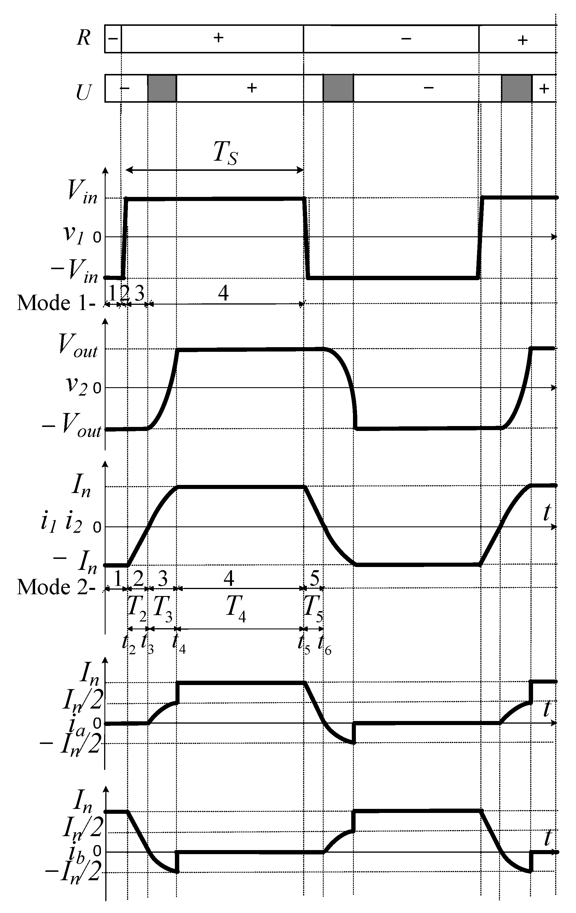
The design example of the circuit parameters for the proposed SR-SAHB converter is derived below. Table 2 lists the specifications and designed parameters of the proposed SR-SAHB converter as a laboratory experimental prototype system. The SR-SAHB converter is designed with the rated specifications of the output power P o u t = 2.45   kW , output voltage 2 V o u t = 265   V , input voltage 2 V i n = 265   V , and transformer frequency f s = 20 kHz.
Because the input and output voltages are the same, the turn ratio of the high-frequency transformer a is designed to be unified.
a = 2 V i n 2 V o u t = 1
Because of the rated transformer frequency f s = 20 kHz, the half period T s is given in the following equation:
T s = 1 2 f s = 25   μ s
The resonant frequency f o should be designed to several times the rated transformer frequency f s , as the proposed SR-SAHB converter operates with partial resonance. In the prototype, the frequency ratio f s / f o = 1 / 3.2 is designed, and the resonant frequency f o , and resonant angular frequency 1 / 2 L C r are given in the following equations:
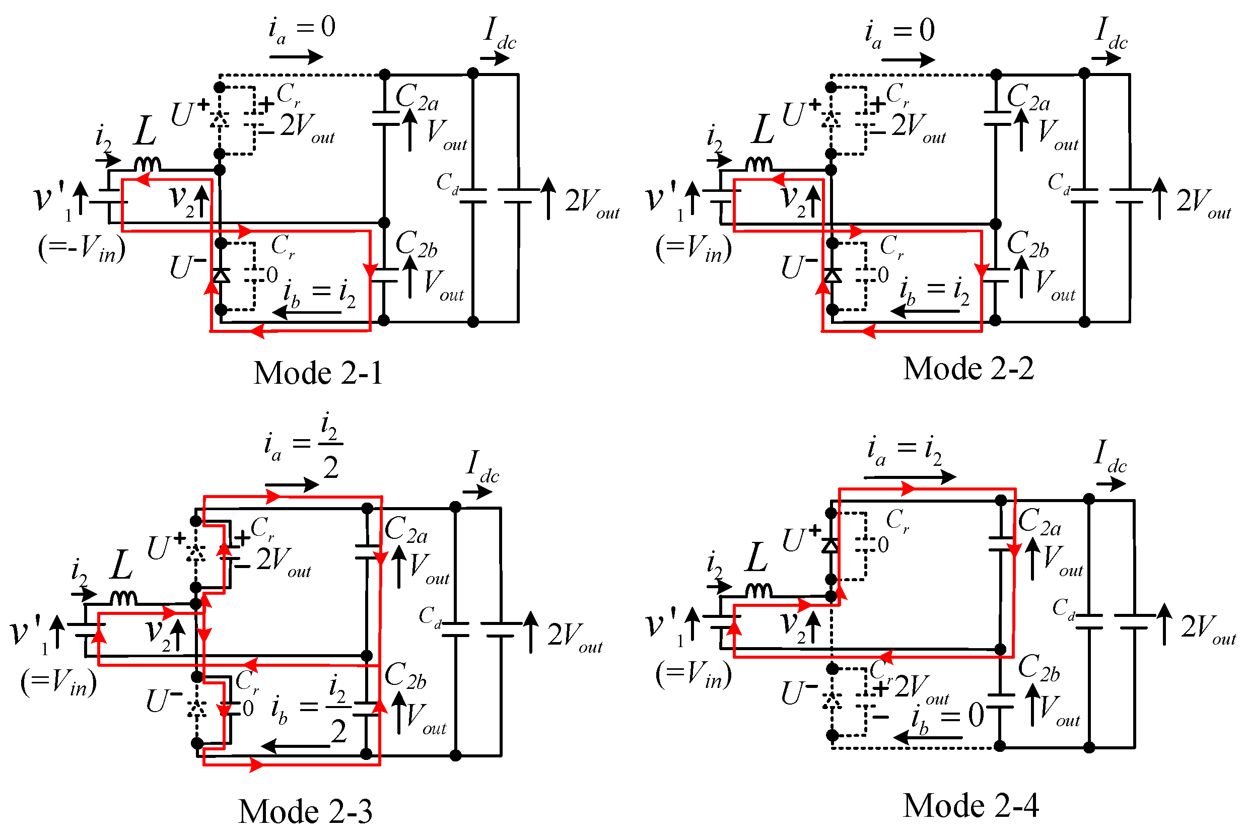
f o = 3.2 f s = 64   kHz
1 2 L C r = 2 π f o 4.0 × 10 5   rad / s
The duration T 3 of Mode 2–3 in Equation (15) and the duration T 5 of Mode 2–5 in Equation (22) are calculated as Equations (37) and (38), respectively:
T 3 = π 2 2 L C r = 3.92   μ s
T 5 = 2 L C r = 2.5   μ s
The amplitude I n of the secondary current i 2 for obtaining the rated power P o u t is calculated from Equations (16) and (26) as follows:
I n = 2 V o u t 2 C r L = P o u t V o u t 1 1 + π 2 T s 2 L C r = 23.3   A
From Equation (39), the characteristic impedance L / 2 C r is obtained by the following equation:
L 2 C r = 2 V o u t I n = 11.4   Ω
From Equations (36) and (40), the leakage inductance L and resonant capacitor C r are designed:
L = 2 L C r L 2 C r = 28.4   μ H
C r = 2 L C r 2 C r L / 2 = 0.11   μ F
In the prototype, TDK transformer ferrite core PC40 is used for a high frequency transformer with the leakage inductance L. The number of turns of the primary and secondary windings is set to 30 for obtaining a large magnetizing inductance without flux saturation at the lowest transformer frequency of 10 kHz. The magnetizing inductance L m = 5.67 mH is obtained. Further, in order to obtain the designed leakage inductance L = 28.4 μH, the overlap ratio of the primary and secondary windings is adjusted by trial and error. The fundamental component I m of the magnetizing current at the rated condition is calculated using the fundamental component of the primary voltage V 1 = 2 / 2 π V i n in the following equation:
I m = V 1 2 π f s L m = V i n 2 π 2 f s L m = 0.084   A
The magnetizing current I m can be neglected as the magnetizing current is small enough, compared with the amplitude I n = 23.3   A of the primary current i 1 = i 2 .
In the primary circuit of Mode 1–2 in Figure 5, the voltage of each soft-switching capacitor C s is changed between 0 and 2 V i n . Half of the primary current i 1 ( = I n / a ) flows to the capacitor. Therefore, the duration T 12 of Mode 1–2 is obtained as follows:
T 12 = 2 C s V i n I n / 2 a
By giving the duration of Mode 1–2 T 12 = 0.2 µs, the soft-switching capacitor C s is designed as follows:
C s = I n T 12 4 a V i n = 8.8 × 10 9 10   nF
To compare with the characteristics of the conventional SAHB converter in Table 1B, the characteristics of the proposed SR-SAHB converter at unity turns ratio a = 1 are calculated. The effective values of the primary current I 1 = 21.5   A in Equation (27), and the total power factor T P F = 0.86 in Equation (28) are obtained using 2 V o u t = 265   V , the leakage inductance L in Equation (41), and the resonant capacitor C r in Equation (42). As mentioned in Section 2, the proposed SR-SAHB converter can operate at the voltage conversion ratio M v = 1.00 , and the peak current and total power factor T P F in Table 1B shows a significant improvement, compared with that of the conventional converter.

5. Experimental Results

The behavior of the 2.45 kW SR-SAHB converter in Table 2 is verified by experiments. The primary half-bridge is composed of two Cree C2M0040120D SiC MOSFETs, and the secondary diode half-bridge is composed of two VS–UFL230FA60 Vishay Schottky diodes. The inductor L = 28.4 µH is the leakage inductance of the high-frequency transformer. The resonant capacitor C r is composed of two 55 nF capacitors in parallel. The dead time T d e a d = 0.2 µs of the primary switches is used in the experimental circuit.
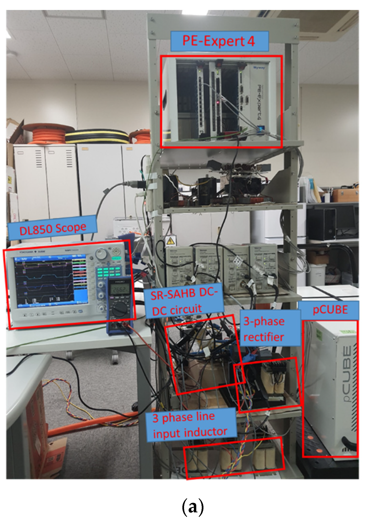
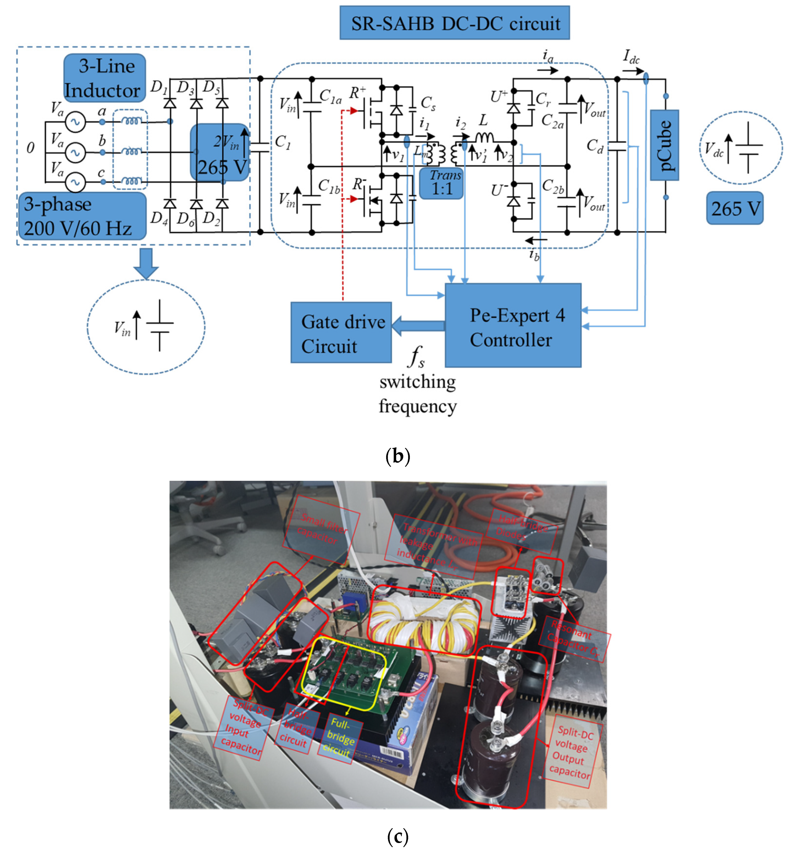
Figure 8a shows the experimental set up of the proposed SR-SAHB DC-DC converter. The input DC voltage 2 V i n = 265   V is obtained by rectifying the three-phase AC voltages of 60 Hz and 200 V using the three-phase full-bridge diode rectifier circuit. The regenerative DC power supply pCUBE is used instead of the 265 VDC battery. The controller was the PE–Expert 4 system using DSP TMS320C6657, and the DL850 Yokogawa was used for measuring the voltage and current waveforms. The measured voltage and current waveforms were obtained directly from the DL850 using the Xviewer software.
Figure 8b shows the electrical diagram of the proposed SR-SAHB DC-DC converter with the detailed descriptions of the circuit that has been presented above in Figure 8a.
Figure 8c shows the prototype of the SR-SAHB DC-DC converter with the half-bridge circuit utilized from the 2 switches in the leading legs of the H-bridge circuit.
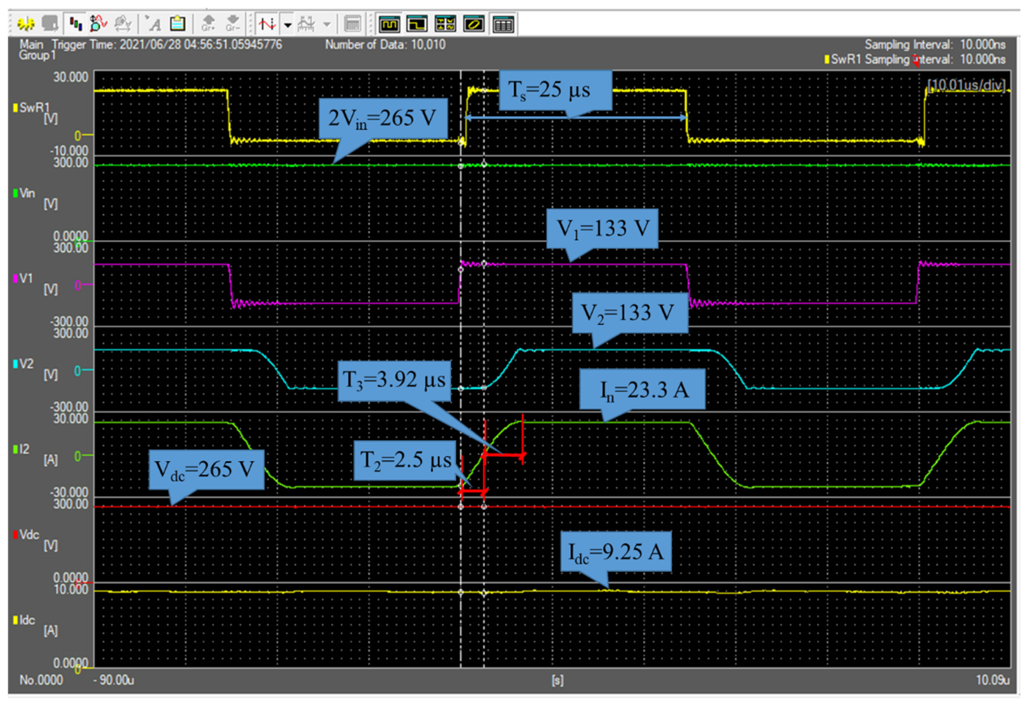
Figure 9 shows the experimental voltage and current waveforms during two periods of the high-frequency transformer at f s = 20   kHz . The waveforms are the gate signal v g of switch R + , input voltage 2 V i n = 265 V primary voltage v 1 , secondary voltages v 2 , output DC voltage 2 V o u t , secondary current i 2 , and output DC current i d c . According to the gate signal v g with the half period T s = 25 µs, the primary voltage v 1 of the amplitude V i n = 133 V and the frequency f s = 20 kHz are generated. The secondary rectangular voltage v 2 of the amplitude V i n = 133 V and the frequency f s = 20 kHz are obtained. The secondary current i 2 flows by the difference between v 1 and v 2 . The amplitude of the secondary current i 2 is the designed value of 23.3 A. The durations T 2 = T 5 = 2.5 µs of Mode 2-2 in Equation (22) and T 3 = 3.92 µs of Mode 2–3 in Equation (15) are obtained. The output DC current I d c is 9.25 A. The experimental results are similar to the theoretical results.
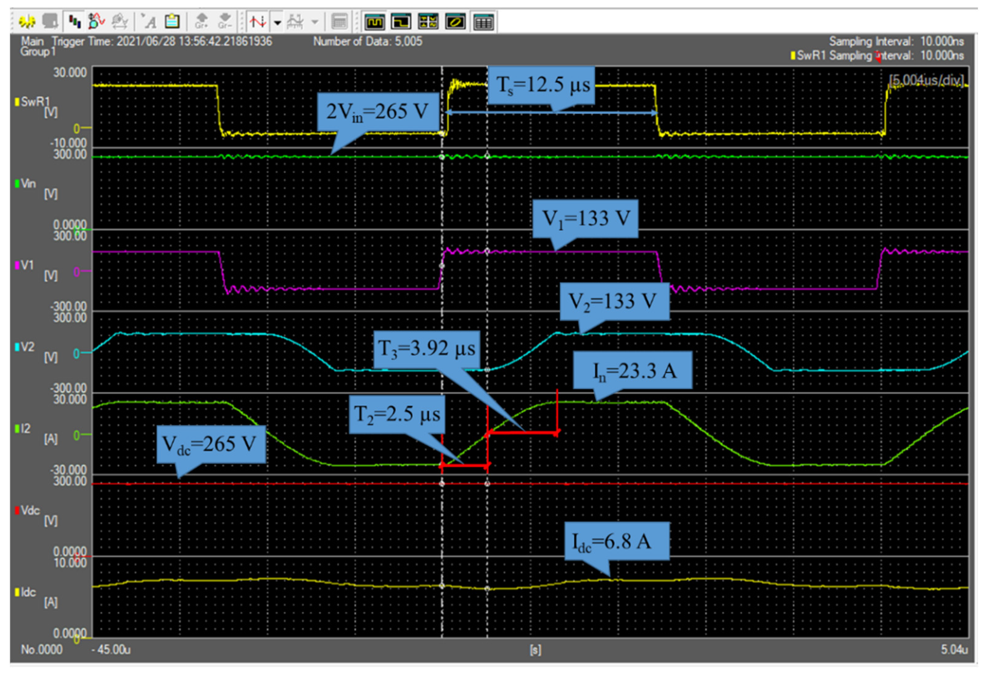
Figure 10 shows the experimental voltage and current waveforms of the high-frequency transformer at f s = 40   kHz . The order of the waveforms shown in Figure 10 is the same as that in Figure 9. According to the gate signal v g with the half period T s = 12.5 µs, input voltage 2 V i n = 265 V, the primary voltage v 1 of the amplitude V i n = 133 V and the frequency f s = 40 kHz are generated. The amplitude of secondary current I n = 23.3   A , the durations T 2 = 2.5 µs of Mode 2–2 in Equation (22) and T 3 = 3.92 µs of Mode 2–3 in Equation (15) are the same as in Figure 8. The duration of Mode 2–4 is shorter than that in Figure 8. As a result, the average output DC current I d c is reduced to 6.8 A.
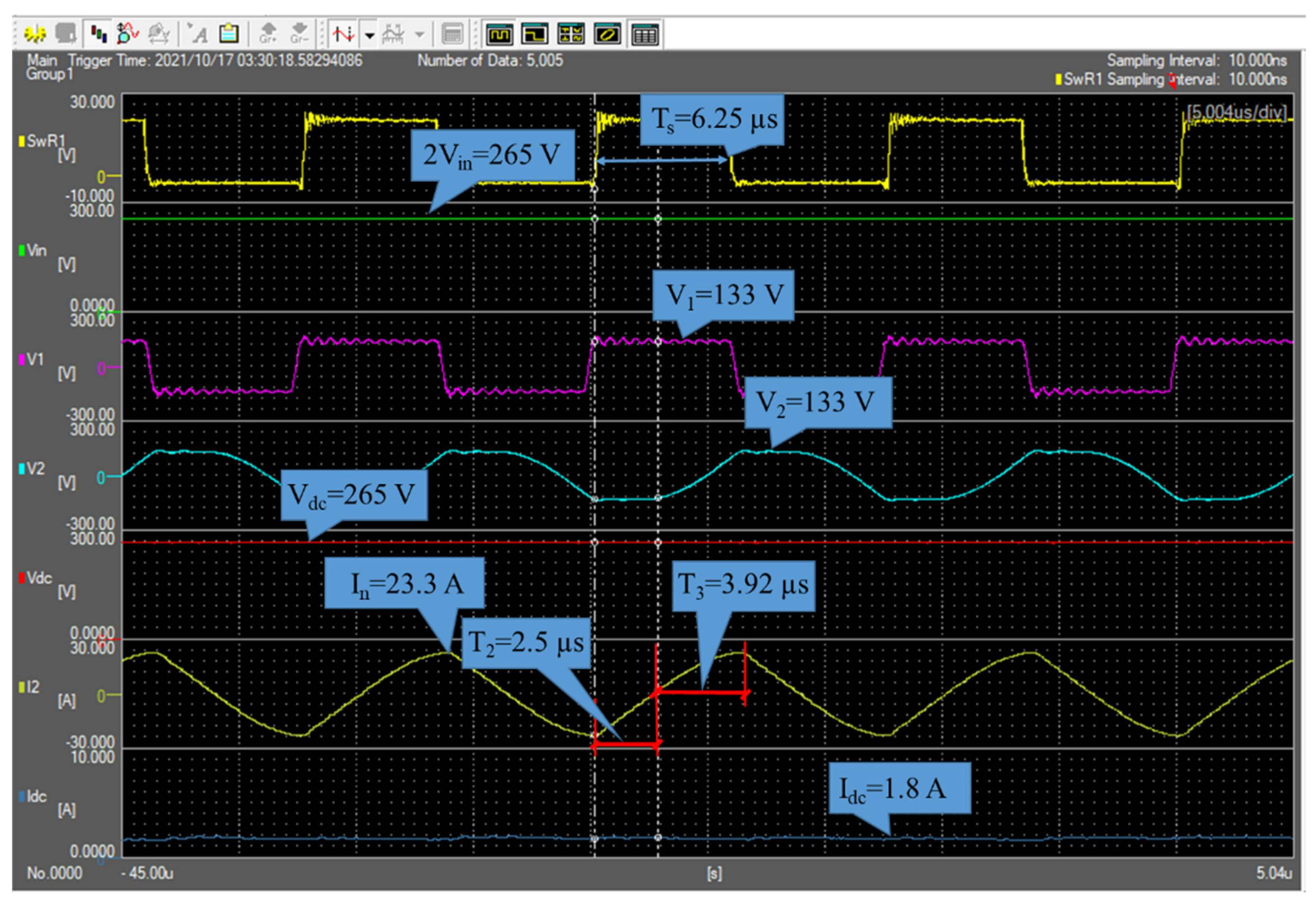
Figure 11 shows the experimental voltage and current waveforms of the high-frequency transformer at f s = 80   kHz . The order of the waveforms shown in Figure 11 is the same as that in Figure 9. According to the gate signal v g with the half period T s = 6.25 µs, input voltage 2 V i n = 265 V, the primary voltage v 1 of the amplitude V i n = 133 V and the frequency f s = 80 kHz are generated. The amplitude of secondary current I n = 23.3   A , the durations T 2 = 2.5 µs of Mode 2–2 in Equation (22) and T 3 = 3.92 µs of Mode 2–3 in Equation (15) are the same as in Figure 9. The duration of Mode 2–4 is 0 µs. As a result, the average output DC current I d c is reduced to 1.8 A. In the light load, since the amplitude of the secondary current is large, the stable soft switching is achieved.
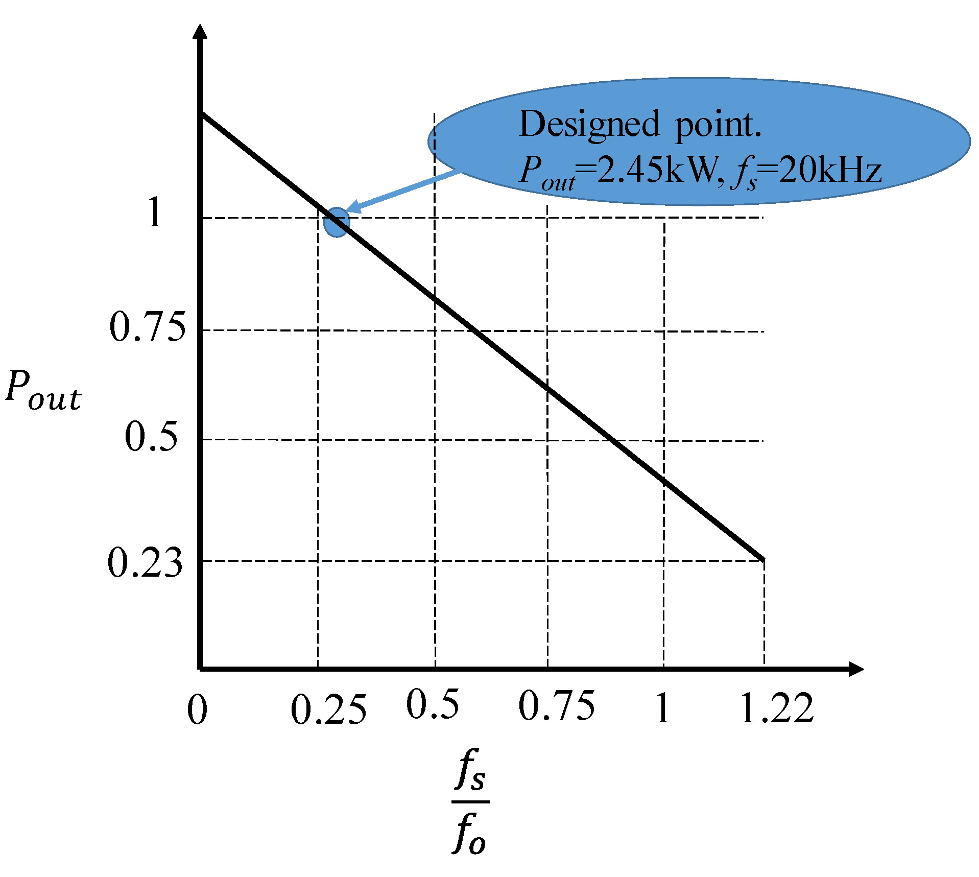
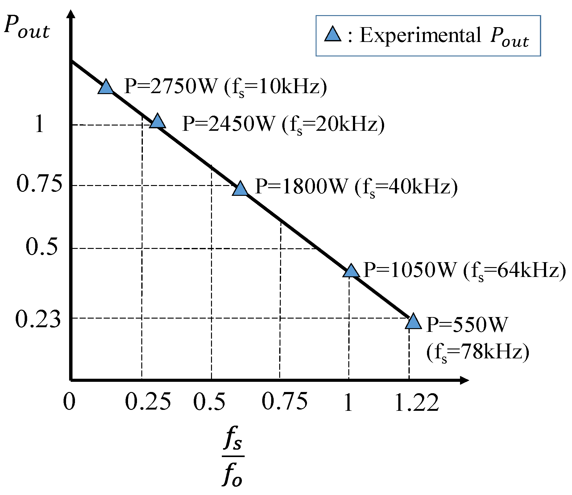
Figure 12 shows the experimental characteristics of the output power P o u t versus the frequency ratio f s / f o . When the transformer frequency f s varies from 10 kHz to 78 kHz, the output power P o u t decreases from 2750 W to 550 W, and the characteristics coincide with the theoretical linear line in Equation (31). The output power P o u t can be regulated over a wide range by adjusting the frequency ratio f s / f o from 0 to 1.22.
Figure 13 shows the efficiency of the converter for the output power range. The input and output powers are measured using a power analyzer (WT1800, YOKOGAWA). A maximum efficiency of 97.3% is achieved at P o u t = 2750   W with the transformer frequency f s = 10   kHz . At the rated output power P o u t = 2.45   kW and the transformer frequency f s = 20   kHz , the measured efficiency of the circuit is 96.3%. At a low output power, P o u t = 550   W and when the transformer frequency f s = 78   kHz , the efficiency is 91.5%. When the transformer frequency f s increases from 10 kHz to 78 kHz, the efficiency decreases owing to the reduction in the output power, and the increase in the switching loss and iron loss of the transformer with a higher transformer frequency.
The high efficiency can be obtained at the rated output. Therefore, the proposed converter is suitable for battery chargers, since the main operation of battery charging is constant power charging at rated power.

6. Conclusions

This paper presented a unidirectional secondary-resonant single-active-half-bridge (SR-SAHB) DC-DC converter using a high-frequency transformer. The analysis and circuit parameter design of the proposed SR-SAHB converter were clarified. The proposed SR-SAHB converter achieved soft-switching at all commutations, unity voltage conversion ratio, and the high total power factor of the high-frequency transformer. A control method for the output power using the transformer frequency was proposed. The characteristics of the proposed SR-SAHB converter were verified by theory and experiments using a laboratory prototype with an output power of 2.45 kW, transformer frequency of 20 kHz, and output DC voltage of 265 V.
The characteristics of the proposed converter for varying the voltage conversion ratio will be clarified in the near future.

Author Contributions

Conceptualization, T.T. and C.A.T.; methodology, C.A.T.; software, C.A.T.; validation, T.T. and C.A.T.; formal analysis, C.A.T.; investigation, C.A.T.; resources, T.T.; data curation, C.A.T.; writing—original draft preparation, C.A.T.; writing—review and editing, T.T. and C.A.T.; visualization, C.A.T.; supervision, T.T.; funding acquisition, T.T. All authors have read and agreed to the published version of the manuscript.

Funding

This work was supported and funded in part by JSPS KAKENHI (Grant Number JP21H01310).

Institutional Review Board Statement

Not applicable.

Informed Consent Statement

Not applicable.

Data Availability Statement

Not applicable.

Conflicts of Interest

The authors declare no conflict of interest.

References

  1. Doncker, R.W.D.; Divan, D.M.; Kheraluwala, M.H. A Three Phase Soft–Switched High–Power–Density DC/DC Converter for High–Power Applications. IEEE Trans. Ind. Appl. 1991, 27, 63–73. [Google Scholar] [CrossRef]
  2. Kheraluwala, M.H.; Gascoigne, R.W.; Divan, D.M.; Baumann, E.D. Performance Characterization of A High–Power Dual Active Bridge DC to DC Converter. IEEE Trans. Ind. Appl. 1992, 28, 1294–1301. [Google Scholar] [CrossRef]
  3. Zhao, B.; Song, Q.; Liu, W.; Sun, Y. Overview of Dual–Active–Bridge Isolated Bidirectional DC–DC Converter for High Frequency–Link Power–Conversion System. IEEE Trans. Power Electron. 2014, 29, 4091–4106. [Google Scholar] [CrossRef]
  4. Peng, F.; Li, H.; Su, G.-J.; Lawler, J. A New ZVS Bidirectional DC–DC Converter for Fuel Cell and Battery Application. IEEE Trans. Power Electron. 2004, 19, 54–65. [Google Scholar] [CrossRef] [Green Version]
  5. Ngo, T.; Won, J.; Nam, K. A single-phase bidirectional dual active half-bridge converter. In Proceedings of the 2012 Twenty-Seventh Annual IEEE Applied Power Electronics Conference and Exposition (APEC), Orlando, FL, USA, 5–9 February 2012; pp. 1127–1133. [Google Scholar]
  6. Zhang, J.; Xu, D.; Qian, Z. An improved dual active bridge DC/DC converter. In Proceedings of the 2001 IEEE 32nd Annual Power Electronics Specialists Conference (IEEE Cat. No.01CH37230), Vancouver, BC, Canada, 17–21 June 2001; pp. 232–236. [Google Scholar] [CrossRef]
  7. Tao, H.H.; Duarte, J.L.; Hendrix, M.A.M. Three-Port Triple-Half-Bridge Bidirectional Converter with Zero-Voltage Switching. IEEE Trans. Power Electron. 2008, 23, 782–792. [Google Scholar] [CrossRef]
  8. Kim, J.; Song, H.-S.; Nam, K. Asymmetric Duty Control of a Dual-Half-Bridge DC/DC Converter for Single-Phase Distributed Generators. IEEE Trans. Power Electron. 2010, 26, 973–982. [Google Scholar] [CrossRef]
  9. Sha, D.; Zhang, J.; Sun, T. Multimode Control Strategy for SiC mosfets Based Semi-Dual Active Bridge DC–DC Converter. IEEE Trans. Power Electron. 2018, 34, 5476–5486. [Google Scholar] [CrossRef]
  10. Hong, T.; Geng, Z.; Qi, K.; Zhao, X.; Ambrosio, J.; Gu, D. A Wide Range Unidirectional Isolated DC-DC Converter for Fuel Cell Electric Vehicles. IEEE Trans. Ind. Electron. 2021, 68, 5932–5943. [Google Scholar] [CrossRef]
  11. Mweene, L.H.; Wright, C.A.; Schlecht, M.F. A 1 kW 500 kHz Front–End Converter for A Distributed Power Supply System. IEEE Trans. Power Electron. 1991, 6, 398–407. [Google Scholar] [CrossRef]
  12. Gu, B.; Lai, J.-S.; Kees, N.; Zheng, C. Hybrid-Switching Full-Bridge DC–DC Converter With Minimal Voltage Stress of Bridge Rectifier, Reduced Circulating Losses, and Filter Requirement for Electric Vehicle Battery Chargers. IEEE Trans. Power Electron. 2012, 28, 1132–1144. [Google Scholar] [CrossRef]
  13. Choi, H.-S. Design Consideration of Half-Bridge LLC Resonant Converter. J. Power Electron. 2006, 7, 13–20. [Google Scholar]
  14. Wei, Y.; Luo, Q.; Du, X.; Altin, N.; Nasiri, A.; Alonso, J.M. A Dual Half-Bridge LLC Resonant Converter with Magnetic Control for Battery Charger Application. IEEE Trans. Power Electron. 2020, 35, 2196–2207. [Google Scholar] [CrossRef]
  15. Awwad, A.E.; Badawi, N.; Dieckerhoff, S. Efficiency analysis of a high frequency PS-ZVS isolated unidirectional full-bridge DC-DC converter based on SiC MOSFETs. In Proceedings of the 18th European Conference on Power Electronics and Applications (EPE’16 ECCE Europe), Karlsruhe, Germany, 5–9 September 2016; pp. 1–10. [Google Scholar] [CrossRef]
  16. Fontana, C.; Forato, M.; Kumar, K.; Outeiro, M.T.; Bertoluzzo, M.; Buja, G. Soft-switching capabilities of SAB vs. DAB converters. In Proceedings of the IECON 2015—41st Annual Conference of the IEEE Industrial Electronics Society, Yokohama, Japan, 9–12 November 2015; pp. 003485–003490. [Google Scholar]
  17. Ting, Y.; De Haan, S.; Ferreira, J.A. The Partial-Resonant Single Active Bridge DC-DC Converter for Conduction Losses Reduction in the Single Active Bridge. In Proceedings of the 2013 IEEE ECCE Asia Downunder, Melbourne, Australia, 3–6 June 2013; pp. 987–993. [Google Scholar]
  18. Li, Y.; Junyent-Ferre, A.; Judge, P.D. A Boost-Full-Bridge-Type Single-Active-Bridge Isolated AC-DC Converter. In Proceedings of the 2019 IEEE Applied Power Electronics Conference and Exposition (APEC), Anaheim, CA, USA, 17–21 March 2019; pp. 2021–2028. [Google Scholar]
  19. Averberg, A.; Mertens, A. Characteristics of the single active bridge converter with voltage doubler. In Proceedings of the 2008 13th International Power Electronics and Motion Control Conference, Poznan, Poland, 1–3 September 2008; pp. 213–220. [Google Scholar]
  20. Demetriades, G.D.; Nee, H.-P. Small-signal analysis of the half-bridge soft-swithing uni-directional converter employing extended state-space averaging. In Proceedings of the 2008 IEEE Power Electronics Specialists Conference, Rhodes, Greece, 15–19 June 2008; pp. 385–391. [Google Scholar]
  21. Zhao, L.; Li, F.; Zhuang, Z.; Li, Z.; Luo, Z. A Dual Half-Bridge Converter with Current Doubler Rectifier. IEEE Trans. Ind. Electron. 2019, 67, 6398–6406. [Google Scholar] [CrossRef]
  22. Tuan, C.A.; Naoki, H.; Takeshita, T. Unidirectional Isolated High-Frequency-Link DC-DC Converter Using Soft-Switching Technique. In Proceedings of the 2019 IEEE 4th International Future Energy Electronics Conference (IFEEC), Singapore, 25–28 November 2019; pp. 595–600. [Google Scholar]
  23. Tuan, C.A.; Takeshita, T. Analysis of Unidirectional Secondary Resonant Single Active Bridge DC–DC Converter. Energies 2021, 14, 6349. [Google Scholar] [CrossRef]
Figure 1. Proposed unidirectional secondary-resonant single-active-half-bridge DC-DC Converter.
Energies 14 07432 g001
Figure 2. Conventional unidirectional single-active-half-bridge DC-DC converter. (a) Circuit configuration. (b) Secondary equivalent circuit.
Energies 14 07432 g002
Figure 3. Voltage and current waveforms of conventional unidirectional SAHB DC-DC converter.
Energies 14 07432 g003
Figure 4. Operating waveforms of proposed SR-SAHB DC-DC converter.
Energies 14 07432 g004
Figure 5. Soft-switching modes of primary half-bridge converter.
Energies 14 07432 g005
Figure 6. Commutations of the secondary diode rectifier circuit.
Energies 14 07432 g006
Figure 7. Output power characteristic with respect to the switching frequency of the transformer.
Energies 14 07432 g007
Figure 8. (a) Proposed SR–SAB DC-DC 265VDC/265VDC converter experimental setup; (b) Proposed SR–SAB DC-DC 265VDC/265VDC converter electrical diagram; (c) Prototype of the SR-SAHB DC-DC 265VDC/265VDC converter.
Energies 14 07432 g008aEnergies 14 07432 g008b
Figure 9. Experimental voltage and current waveforms at f s = 20   kHz .
Energies 14 07432 g009
Figure 10. Experimental voltage and current waveforms at f s = 40   kHz .
Energies 14 07432 g010
Figure 11. Experimental voltage and current waveforms at f s = 80   kHz .
Energies 14 07432 g011
Figure 12. Characteristics of output power P o u t versus switching frequency ratio f s / f o .
Energies 14 07432 g012
Figure 13. Efficiency versus output power characteristics.
Energies 14 07432 g013
Table 1. Design example of conventional SAHB and proposed SR-SAHB converters on 2.45 kW output power.
(A) Specifications
Output power P o u t 2.45 kW
Output voltage 2 V o u t 265 V
Turns ratio a 1
Leakage inductance L 28.4 μ H
Transformer frequency f s 20 kHz
(B) Comparisons of Designed Parameters
ConverterConventionalProposed SR-SAHB
Input voltage 2 V i n 362 V265 V
Voltage conversion ratio M v 0.731.00
Peek current37.0 A23.3 A
Effective current value I 1 21.7 A21.5
Total power factor T P F 0.630.86
Resonant capacitor C r -0.11 μ F
Table 2. Specifications and designed parameters of proposed apb converter.
(A) Rated Specifications
Output power P o u t 2.4 kW
Output voltage 2 V o u t 265 V
Input voltage 2 V i n 265 V
Transformer frequency f s 20 kHz
(B) Designed Parameters
Turns ratio a 1
Number of turns of primary winding30
Number of turns of secondary winding30
Frequency ratio f s / f o 1/3.2
Leakage inductance L 28.4 μ H
Magnetizing inductance L m 5.67 mH
Resonant capacitor C r 110 nF
Soft-switching capacitor C s 10 nF
DC Capacitors C 1 a , C 1 b ,   C 2 a ,   C 2 b 1500 μ F
Publisher’s Note: MDPI stays neutral with regard to jurisdictional claims in published maps and institutional affiliations.

