1. Introduction
In 1991, the isolated bidirectional DC–DC converter, which adopts the dual-active-bridge (DAB) configuration and uses a soft-switching technique to achieve high efficiency, was proposed [
1]. The transferred power of the DAB converter is regulated by the induced voltage drop on the inductor produced by the relative position of different phase shift angles between the primary and secondary transformer AC voltages. The soft-switching pattern of the DAB converter was resolved during this process [
2]. The DAB converter achieved a high total power factor (TPF) at the high frequency transformer and a unity voltage conversion ratio under the unity transformer turns ratio. Many papers related to DAB converters have been published [
3]. Papers on the soft-switching control method in the low power supply range [
4,
5] and the utilization of GaN FETs to construct high-efficiency converters [
6] have also been published. In an additional study, a DAB converter was applied to an LED driver [
7].
Several circuit topologies of unidirectional isolated DC–DC converters have been proposed for their application in battery chargers. One unidirectional topology based on the DAB converter is a configuration in which two switches in the secondary H-bridge converter are replaced with diodes. For wide-range operation, three operation modes of boost, buck-boost, and buck are proposed [
8]. The light-load conversion efficiency was improved significantly by using the proposed control strategy [
9].
The unidirectional configuration, with the diode rectifier circuit adding the choke coil in the secondary circuit, can obtain high efficiency [
10]. The topology achieved a high TPF at the high-frequency transformer and a unity voltage conversion ratio under the unity transformer turns ratio. However, a voltage surge occurred, owing to the resonance between the transformer leakage inductance and the inherent parasitic capacitance associated with the secondary diodes. To suppress the voltage surge, an RCD snubber circuit was installed at the output of the diode bridge rectifier circuit [
11]. A hybrid-switching converter was then proposed to achieve minimal voltage stress of the diode bridge rectifier circuit [
12].
Another unidirectional topology of an SAB converter is a simpler configuration in which the secondary H-bridge of the DAB converter is replaced with a diode bridge rectifier circuit. When this was trialed, the SAB converter achieved soft switching in the same way as the DAB converter [
13]. The partial resonant SAB converter, in which a capacitor is connected to each primary switch in parallel, was proposed to reduce the peak current and conduction loss [
14]. By utilizing SiC switching devices in DC–DC circuits, high-efficiency performance was achieved [
15]. Papers on the application of the SAB converter to the wind turbine converter were published [
16,
17]. However, the SAB converter does not operate at the unity voltage conversion ratio. Therefore, the DC voltage conversion ratio and the total power factor of the transformer in the SAB converter were low [
1].
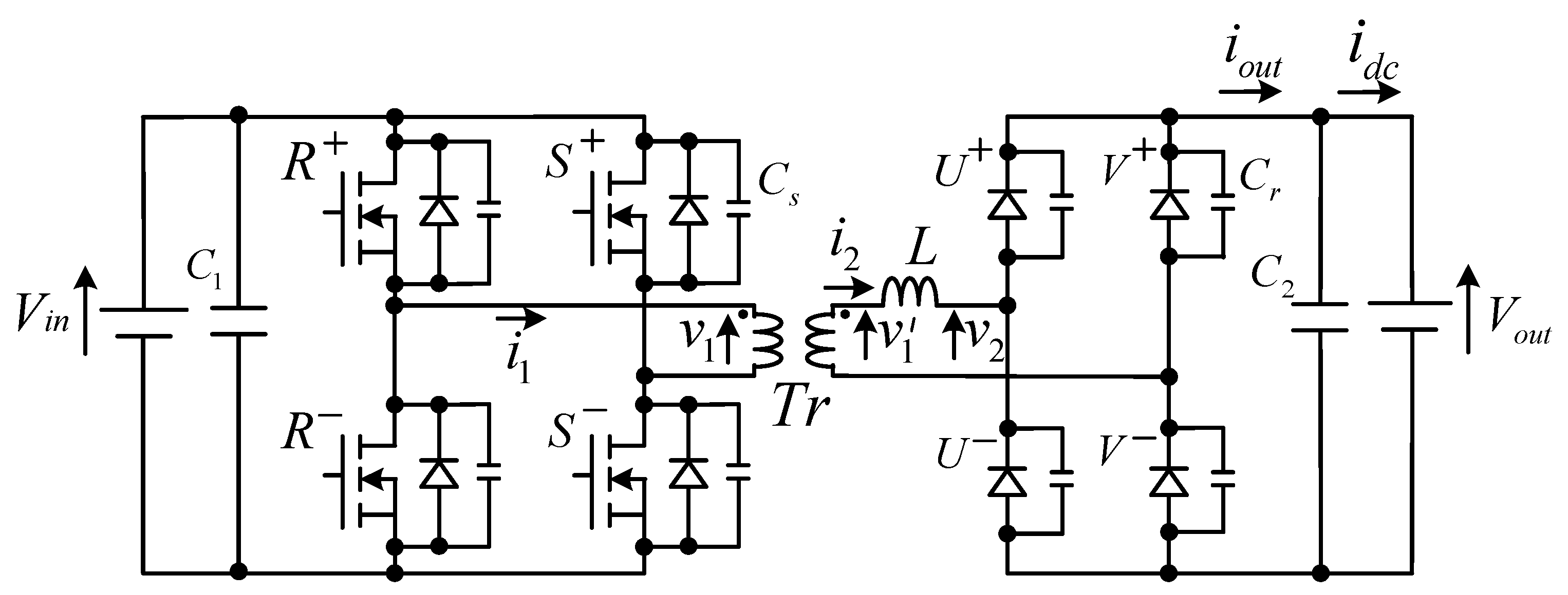
This paper presents a novel, unidirectional, high-frequency isolated DC–DC converter called a secondary resonant single active bridge (SR–SAB) DC–DC converter, as shown in
Figure 1 [
18]. In the SR–SAB DC–DC converter, a resonant capacitor
is connected in parallel to each diode in the secondary rectifying diode circuit of the SAB converter. A trapezoidal transformer current waveform, similar to that of a DAB converter, is obtained because the transformer current sign at the zero-crossing region is softly switched by the series resonance between the transformer leakage inductance
and the resonant capacitors
of the secondary diodes. As a result, the SR–SAB converter reaches the unity DC voltage conversion ratio and improves the total power factor of the transformer compared with the SAB converter. The behavior and design of the proposed SR–SAB converter will be explained. The transformer frequency which is equal to the switching frequency can be independently selected at a frequency lower than the resonant frequency. The leakage inductance can be designed to be sufficiently small enough to be incorporated into the high-frequency transformer. The output power can be adjusted over a wide range by controlling the transformer frequency.
The effectiveness of the proposed converter is verified through experiments using a 1 kW, 48 V, and 20 kHz rating laboratory prototype.
2. Conventional SAB DC–DC Converter
Figure 2 shows the conventional SAB DC–DC converter. In the circuit configuration of
Figure 2a, the SAB converter is comprised of a primary H-bridge converter, an isolated high-frequency transformer, and a secondary rectifying diode bridge circuit. The primary H-bridge converter is constructed from four switches,
, with the small soft-switching capacitor
in parallel. The leakage inductance
L of the transformer is expressed as the equilavent leakage inductance converted to the secondary side. By denoting the number of turns of the transformer’s primary coil with
, and the number of turns of the transformer’s secondary coil with
, the turns ratio can be expressed as
.
Figure 2b shows the secondary equivalent circuit. The primary voltage component
, which transfers the primary voltage
to the secondary side, is represented as the voltage across the secondary magnetizing inductance of the transformer.
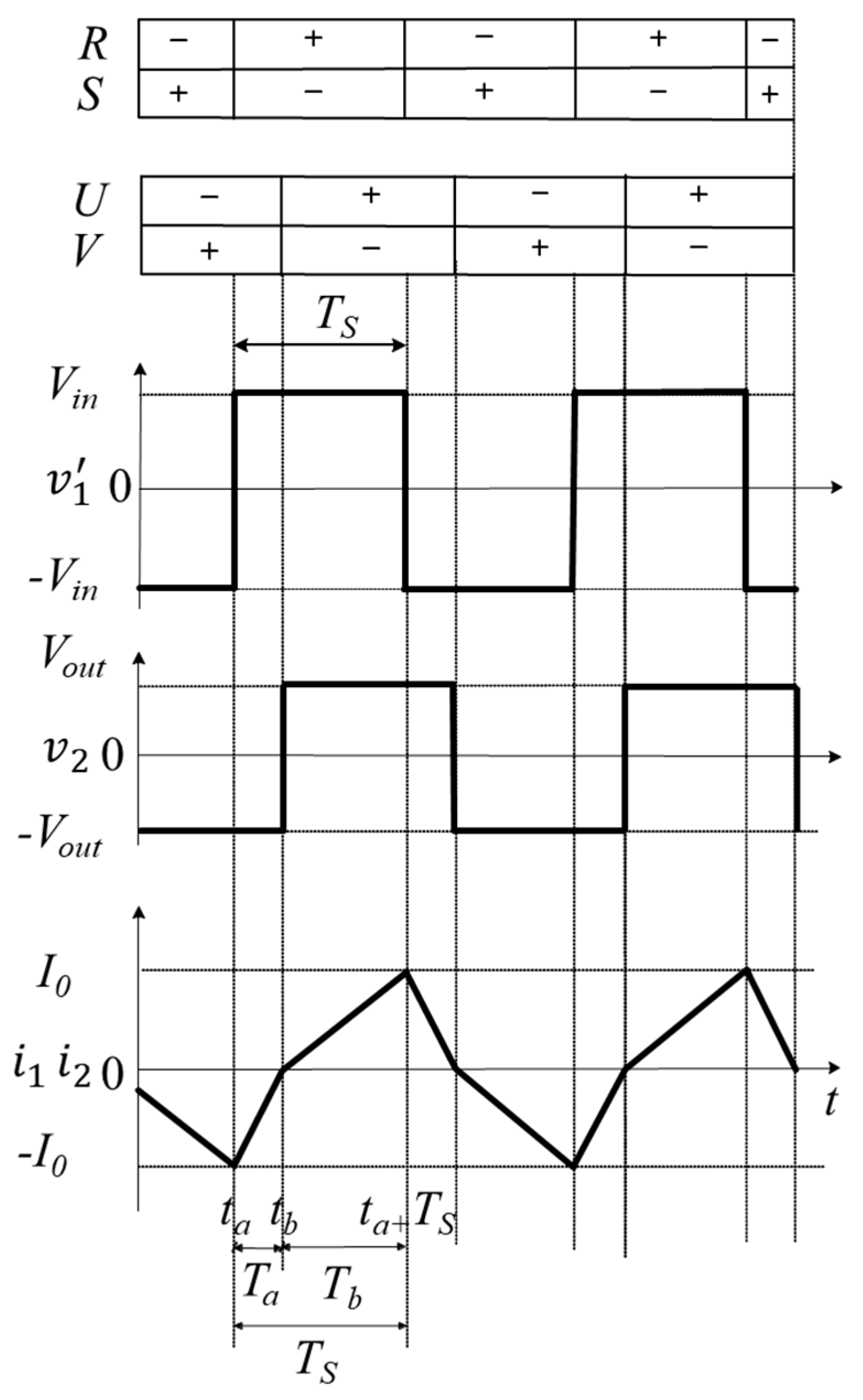
Figure 3 shows the voltage and current operation waveforms of the transformer in the steady state of the conventional unidirectional SAB converter. The conditions of the waveforms are presented at a unity turns ratio of
for the isolated transformer while neglecting the transformer magnetizing current. The primary H-bridge converter generates a square AC voltage
with the amplitude of the input DC voltage
, and frequency
by controlling the switches
with a 50 percent duty cycle. If the amplitude
of the primary voltage
is equal to the output DC voltage
in
Figure 3, the secondary diodes
cannot be turned on, and no power is sent to the secondary side in the SAB converter. Therefore, the SAB converter does not work at a unity DC voltage conversion ratio
. In the voltage waveforms in
Figure 3, the amplitude
of the primary voltage
is higher than the output DC voltage
. The transformer currents
and
flow because of the difference in voltage between the primary voltage
and the output DC voltage
.
The analytical transformer current
in the positive half period
of primary voltage
is derived. From
Figure 2b, the following voltage equation is obtained:
In the duration
, the primary voltage
in
Figure 3 is larger than the output DC voltage
and the negative transformer current
flows. The diodes
and
are in the on-state. Substituting
,
, and the initial current
into (1), the secondary current
in the duration
is obtained as follows:
Because the secondary current
in (2), the duration
is obtained in (3):
In the duration
, the positive transformer current
flows and the diodes
and
are in the on-state. Substituting
and
into (1), the secondary current
in the duration
is obtained as follows:
The duration
is expressed using (3) in (5):
Because the secondary current
in (4), the peak current
is solved as follows:
Substituting
in
Figure 3 into Equations (3) and (5), the durations
and
are obtained as follows:
The total power factor
of the primary side is defined in (9) by using the output power
and the effective values of voltage
and current
:
The output power
can be calculated using the following equation:
The effective value of primary current
is calculated as follows:
Substituting (10), (11), and the effective values of primary voltage
into (9), the total power factor
is obtained as follows:
A design example of the conventional SAB and proposed SR–SAB converters are explained.
Table 1 shows the common specifications of the converter set at
,
, and
.
Table 2 shows the comparisons of calculated characteristics between the conventional and proposed converters. In the conventional converter, the input DC voltage
, the voltage conversion ratio
, the peek current
, and the total power factor
. The characteristics of the proposed SR–SAB converter in
Table 2, which are derived from the theory in
Section 4, improves significantly compared with those of the conventional converter.
3. Unidirectional Secondary Resonant Single Active Bridge (SR–SAB) DC–DC Converter
3.1. Main Circuit Configuration and Behavior
The circuit configuration of the proposed unidirectional SR–SAB DC–DC converter in
Figure 1 adds the resonant capacitor
in parallel with the secondary diodes
in the conventional SAB converter shown in
Figure 2.
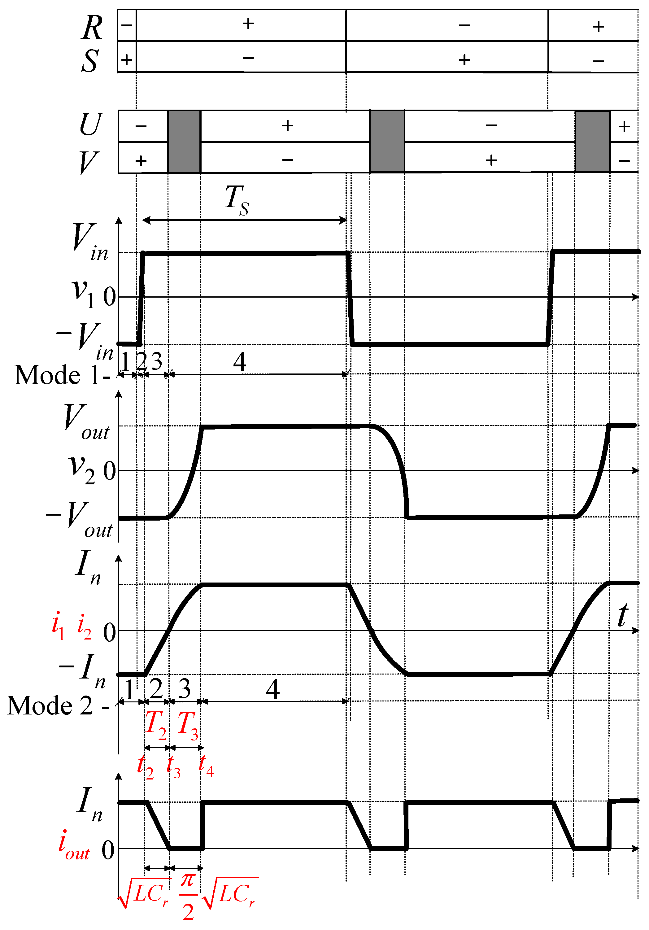
Figure 4 shows the voltage and current operation waveforms of the transformer as it corresponds to the proposed SR–SAB converter given the condition that the unity turns ratio
for the high-frequency transformer while neglecting the transformer magnetizing current. The SR–SAB converter achieves the unity input and output voltage conversion ratio
.
The primary H-bridge converter produces the rectangular AC voltage with the amplitude and switching frequency by alternately switching the switches with a 50 percent duty cycle. The secondary voltage with the rectangular waveform lagged by the primary voltage is obtained. The magnetizing current is very small and neglected, leading to the production of the identical trapezoidal current waveforms for the primary current as well as the secondary current. The rectified current flows according to the conditions of the on-state diodes.
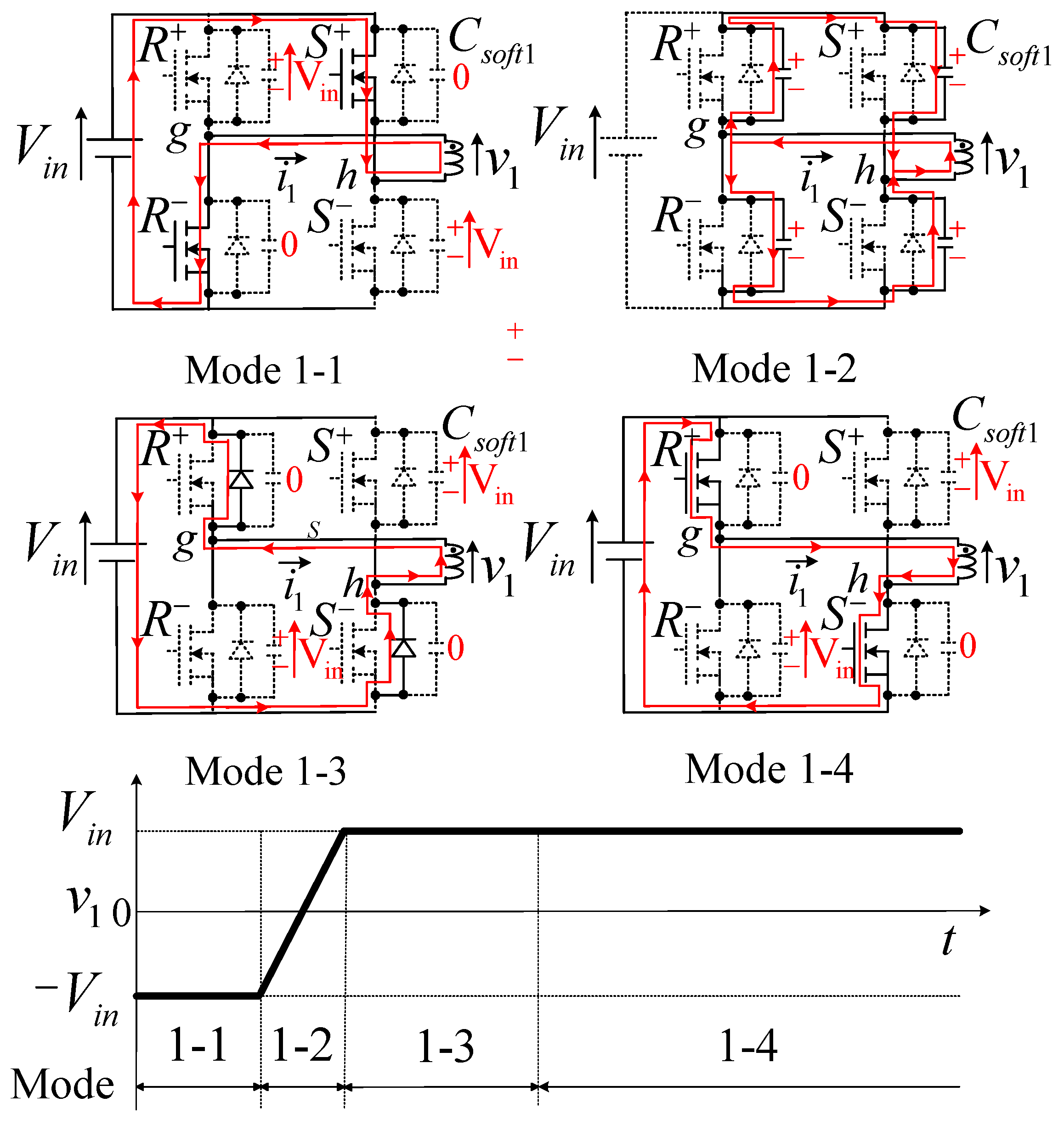
3.2. Soft-Switching Commutation of Primary Converter
The primary converter achieves soft switching in all commutations.
Figure 5 shows the soft-switching modes of the primary H-bridge converter from
and
switches to
and
switches.
In Mode 1−1, and switches are in the turn-on state, generating the primary voltage of . Primary current with negative value is conducted through and switches. The voltages on the parallel capacitors of and switches are kept at zero. When and switches are changed to the turn-off state, zero voltage switching (ZVS) of and switches is obtained because the voltage of the parallel capacitors are zero. After that, the circuit changes to Mode 1–2.
In Mode 1–2, the primary current with the negative value starts to flow through the four capacitors. The voltage of the parallel capacitors of and switches increases, and the voltage of the parallel capacitors of and switches decreases. The primary voltage interchanges from to . When the voltages on parallel capacitor of and switches is reduced to zero, the anti-parallel diodes on and switches are switched to the turn-on state and start conducting. After that, the circuit changes to Mode 1–3.
In Mode 1–3, the switching-on gate signals for and switches are given, leading the primary current to increase continuously toward zero. When the sign of the primary current changes to positive, the circuit changes to Mode 1–4.
In Mode 1–4, and switches are changed to the on-state by zero-voltage switching because of the zero voltage of the parallel capacitor.
3.3. Operation Analysis of Secondary Diode Rectifier Circuit
Figure 6 shows the commutation modes in the secondary side of the diode rectifying circuit, swapping between the pair of diodes
and
and the pair of diodes
and
under the unity input and output voltage conversion ratio
.
In Mode 2-1, the primary voltage of is generated, and the secondary current with negative value flows though the pair of diodes and . The voltages on parallel capacitors of diodes and are both zero, and the voltages on parallel capacitors of diodes and are fully charged to the value of output voltage. When the value of primary voltage changes from to at the time , the circuit starts to enter Mode 2–2.
In Mode 2–2, within the duration
, the primary voltage
changes to the positive value
. The diodes
and
remain on-state, and the negative transformer current
flows. Substituting
,
and the initial current
into formula (1), the equation regarding the secondary current
in Mode 2–2 can be derived as follows:
The secondary current
increases linearly toward zero value, which is shown in
Figure 4. Upon the timing
the secondary current
reaches zero, and Mode 2–2 is completed. The duration
of Mode 2–2, is obtained from (13) by the following equation:
At , all four diodes of the secondary rectifier circuit change to turn-off state, and then Mode 2–3 begins.
In Mode 2–3, the voltages on parallel capacitors
of diodes
and
are both zero, and the voltages on parallel capacitors
of diodes
and
are both charged to the output voltage
at
. The inductor
L, together with four capacitors
, forms an
LC resonating circuit and the resonance occurs. Due to the symmetry property of the circuit, the secondary current flow through each pair of capacitors
with the half value
. Therefore, in Mode 2–3, the voltage equation is formulated as follows:
Substituting
and
into (15), the secondary current
in the duration
of Mode 2–3 is obtained as follows:
The secondary voltage
is derived utilizing the secondary current
in Equation (16) as follows:
The secondary current
and voltage
in (16) and (17) are both sinusoidal waveforms, which are shown in
Figure 4. When the secondary current
becomes
and voltage
becomes
at
, simultaneously, Mode 2–3 is completed. Because at
, the phase angle is
as in
Figure 4, the amplitude value
of the secondary current
and the duration
in Mode 2–3 are obtained from (16) and (17) by the following equations:
The secondary current
in Mode 2–2 in (13) and duration
in (14) is applied to Equation (18), and is rewritten in the following equations:
At
, the voltages on the parallel capacitors of the diodes
and
reduce to zero, then the diodes
and
start conducting, and the circuit shifts to Mode 2–4 in
Figure 6.
In Mode 2–4, substituting the primary voltage
, the secondary voltage
, and the initial value of the secondary current
into (1), in Mode 2–4, the secondary current
is given by the following equation:
The output power
is calculated by the average transferring power for the half period
of the isolated high-frequency transformer using the rectified current
in
Figure 4:
The effective value of primary current
is calculated as follows:
Substituting (23), (24), and
, into (9), the total power factor
is obtained as follows:
3.4. Output Power Control by Frequency Variation
Under the condition of the unity input and output voltage conversion ratio
, the output power
in (23) is a function of the half period
of the high-frequency transformer. If the half period
is shorter than that in
Figure 4, the duration of Mode 2–4 is shorter and the output power
decreases. The output power
can be controlled by the transformer frequency
given by the following equation:
The resonant frequency
in the circuit is given in (27):
Substituting (26) and (27) into (23), the output power
is rewritten as a function of the frequency ratio
as follows:
Figure 7 shows the characteristics of the output power
with respect to the frequency ratio
based on (28). The resonant frequency is determined by the circuit parameters and is a constant value.
By increasing the transformer frequency
, the output power
can be reduced. In
Figure 7, the output power is notarized as
at the frequency ratio
= 1/4. The maximum frequency ratio
is the condition in which the duration of Mode 2–4 in
Figure 4 is zero. Because it means
, the maximum frequency ratio
is given by the following equation:
The highest transformer frequency satisfying the output power
of (28) is
. In
Figure 7, the output power
at
can be reduced to 0.23 of the rated output power
. When the frequency ratio is higher than
, the output power
can be reduced further than that in (28).
4. Design of Circuit Parameters
The design and calculation method for the circuit parameters of the proposed SR–SAB converter are introduced here.
Table 3 shows the specifications and designed parameters of the proposed SR–SAB converter in a laboratory experimental system. The SR–SAB converter is designed with the rated specifications of output power
, output voltage
, input voltage
, transformer frequency
= 20 kHz, and frequency ratio
. The turn ratio of the high-frequency transformer
is equal to the ratio of the input and output voltages, as seen below:
Because transformer frequency is selected as
= 20 kHz, the half-cycle period
, resonant frequency
, and resonant angular frequency
are given in the following equations:
The duration
of Mode 2–2 in (21) and the duration
of Mode 2–3 in (19) are calculated as (34) and (35), respectively.
The amplitude
of the secondary current
is obtained from (18) and (23) as follows:
From (36), the characteristic impedance
is obtained the following equation:
From (33) and (37), the leakage inductance
and resonant capacitor
are determined:
Regarding to the primary H-bridge converter of Mode 1–2 in
Figure 5, each soft-switching capacitor
is changed between 0 and voltage
. Half of the primary current
flows to the capacitor. Therefore, the duration
of Mode 1–2 is obtained as follows:
By giving the duration
= 0.1 μ
s of Mode 1–2, the soft switching capacitor
is designed as follows:
In order to compare them with the characteristics in
Table 2, the characteristics of the proposed SR–SAB converter at unity turn ratio
are calculated. The effective values of the primary current
in (24) and the total power factor
in (25) are obtained using
, the leakage inductance
in (38), and the resonant capacitor
in (39). As mentioned in
Section 2, the proposed SR–SAB converter can operate at a voltage conversion ratio
, and the peak current and total power factor
in
Table 2 show significant improvement compared with those of the conventional SAB converter.
5. Experimental Results
The operation and behavior of the 1 kW, 265 V/48 V SR–SAB converter described in
Table 3 is verified by experimental waveforms. The primary H-bridge is composed of four Rohm SCT3022AL SiC MOSFETs, and the secondary diode bridge is composed of four VS–100BGQ100 Schottky diodes. The inductor value
L = 7.7 μH is derived from the leakage inductance of the high-frequency transformer. Furthermore, the resonant capacitor
is composed of one 330 nF and two 100 nF film capacitors in parallel. The dead time
= 0.2 μs of the primary switches is used in the experimental circuit.
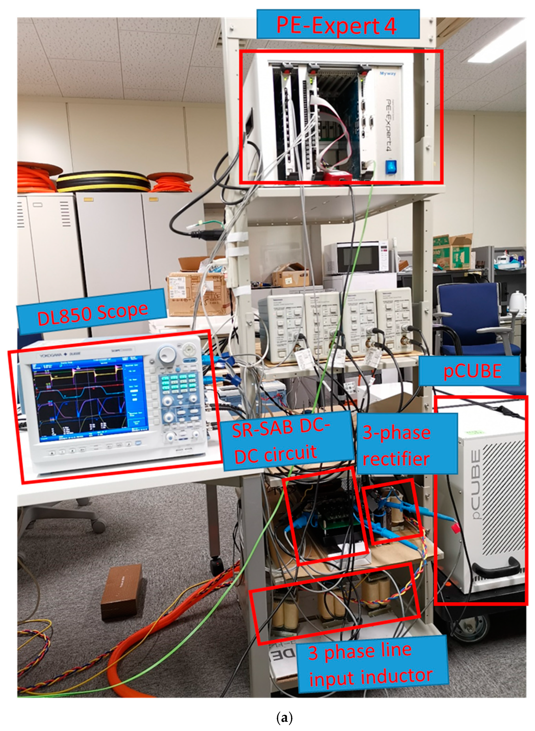
Figure 8a shows the experimental set up of the proposed SR–SAB DC–DC converter. The DC input source
is obtained from the three-phase full-bridge diode rectifier circuit from the three-phase supply voltages of 60 Hz and 200 V, while the 48 V DC load is the regenerative dc power supplier, pCUBE. The controller is the PE–Expert 4 system using DSP TMS320C6657, and the DL850 Yokogawa is used for measuring the voltage and current waveforms. Finally, Xviewer displaying software is used for displaying the voltage and current waveforms directly from the DL850.
Figure 8b shows the electrical diagram of the proposed SR–SAB DC–DC converter with the detailed descriptions of the circuit that has been presented above in
Figure 8a.
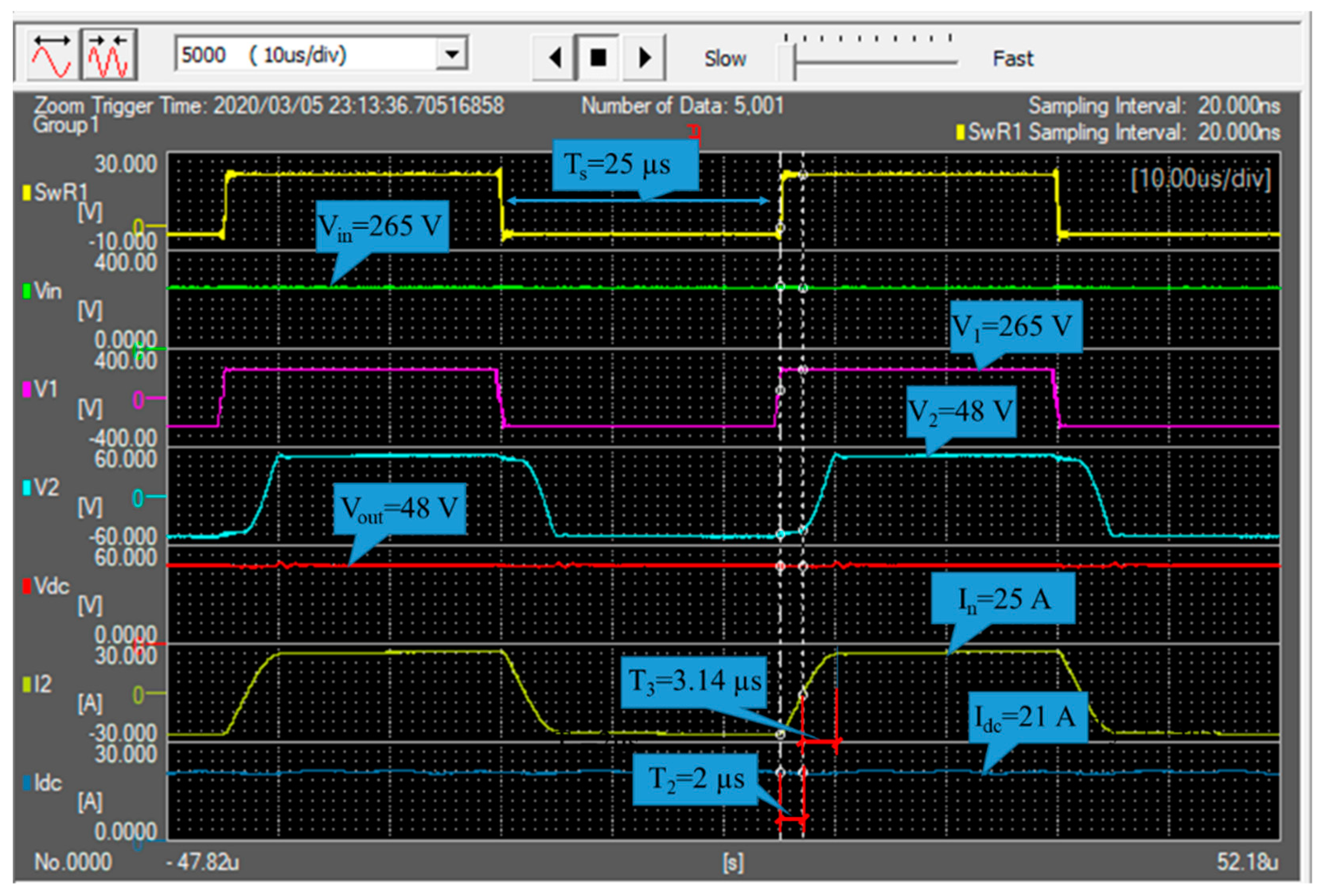
Figure 9 shows the experimental voltage and current waveforms during two periods of the high-frequency transformer at
. The sequential waveforms are the gate driving signal
of the switch
, primary H-bridge voltage
, transformer secondary side voltages
, output DC voltage
, secondary side current
, and output DC current
. The gate signal
and the half period
= 25 μs generates the primary H-bridge voltage
with the amplitude
= 265 V and switching frequency
= 20 kHz. The secondary rectangular waveform voltage
is also observed. The secondary current
flows in the circuit according to the difference in the phase-shift angle between
and
. The amplitude
of the secondary current
is at the designed value of 25 A. The duration
= 2 μs of Mode 2–2 in (34) and
= 3.14 μs of Mode 2–3 in (35) are obtained. The average output DC current
is 21 A. All the experimental waveform results are similar to the theoretical results.
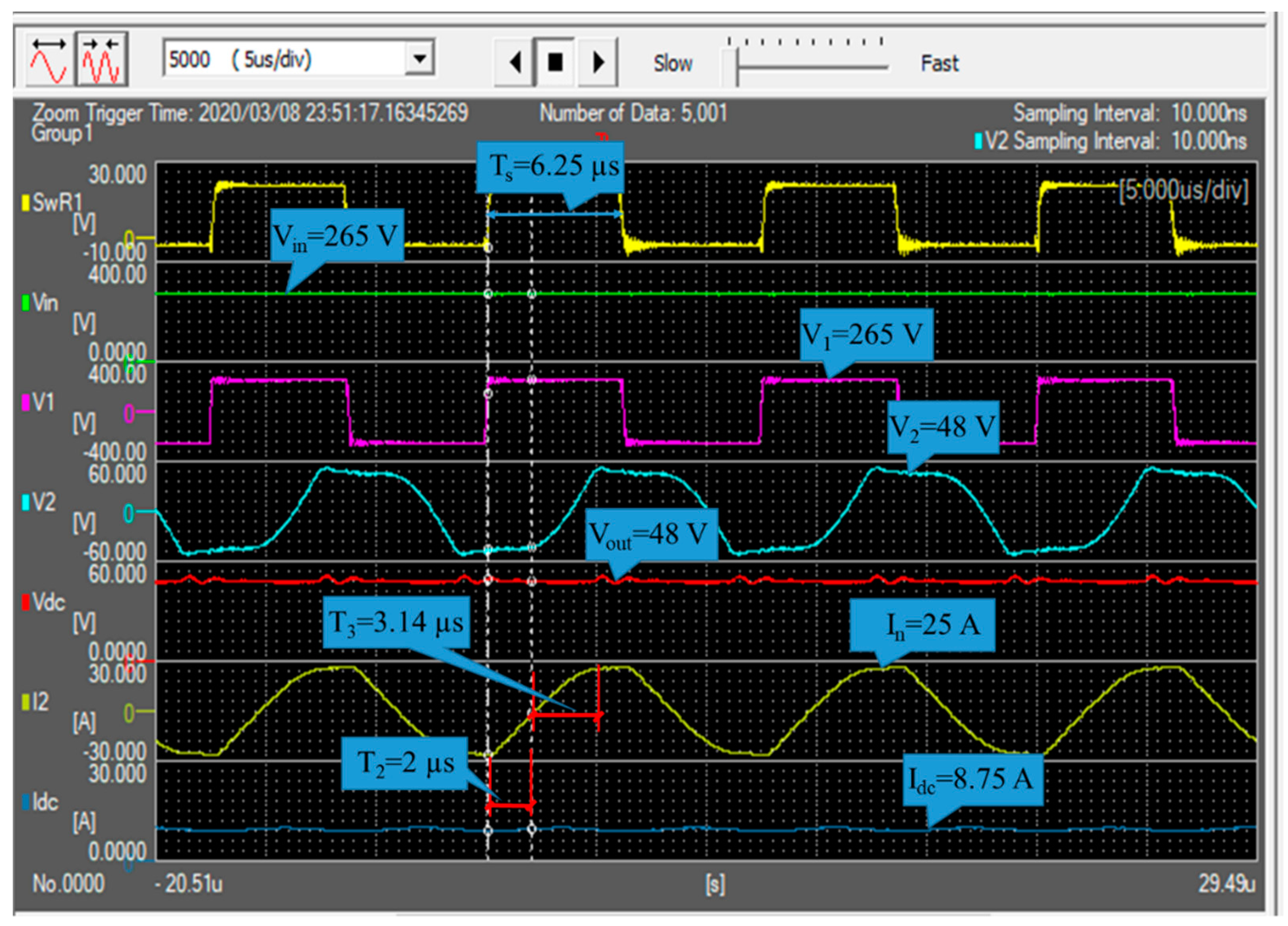
Figure 10 shows the experimental voltage and current waveforms of the isolated high-frequency transformer at
. The order of the waveforms shown in
Figure 10 is the same as that in
Figure 9. The gate driving signal
with the half period
= 6.25 μs generates the primary H-bridge voltage
with the amplitude
= 265 V and the switching frequency
= 80 kHz. The amplitude
of the secondary current
, while the duration
= 2μs of Mode 2–2 in (34) and
= 3.14 μs of Mode 2–3 in (35) are the same as in
Figure 9. The duration of Mode 2–4 is shorter than that in
Figure 9. As a result, the average output DC current
is reduced to 8.75 A.
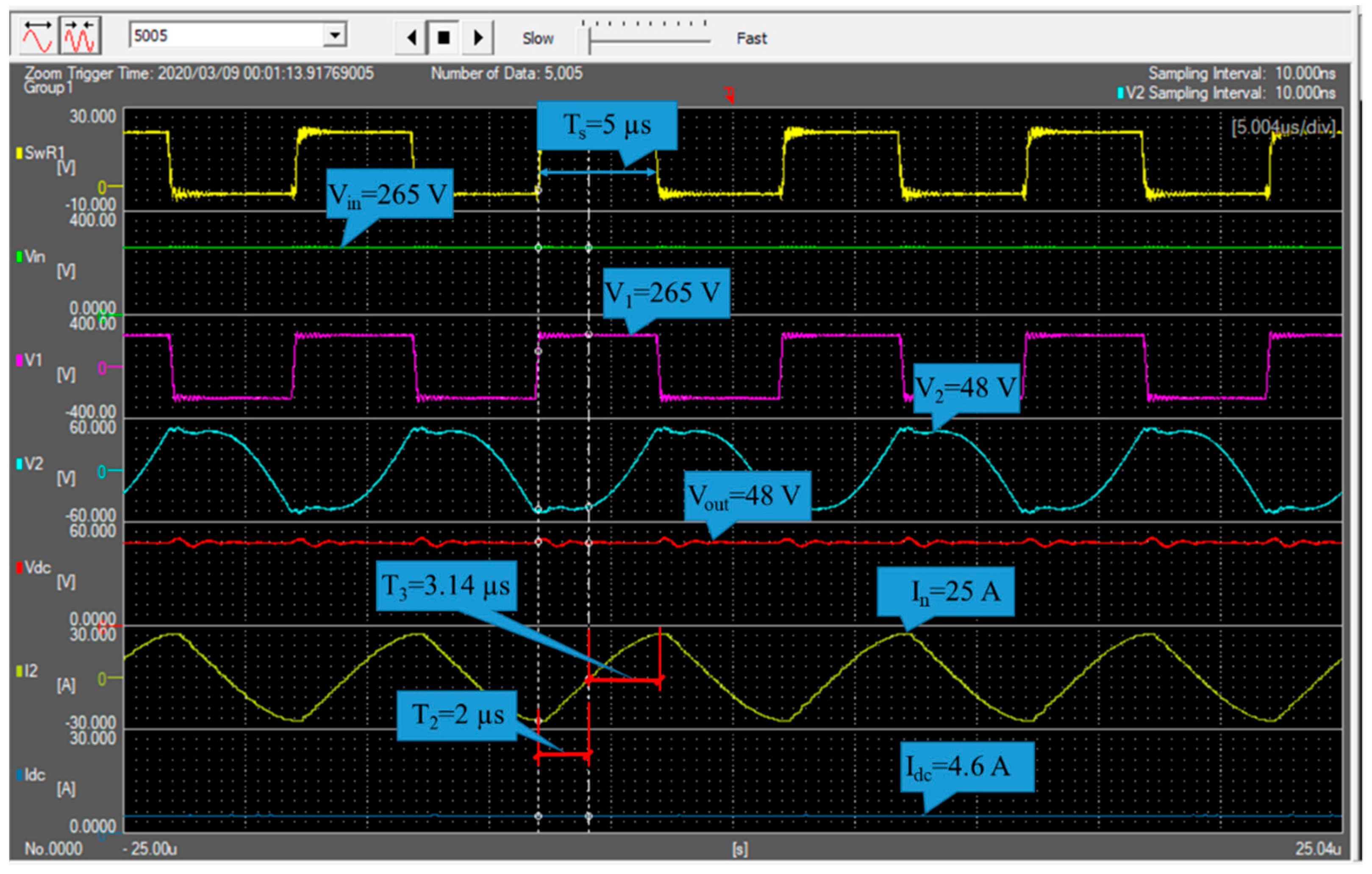
Figure 11 shows the experimental voltage and current waveforms of the isolated high-frequency transformer at
. The order of the waveforms shown in
Figure 11 is the same as that in
Figure 9. The gate driving signal
with the half period
= 5 μs generates the primary H-bridge voltage
with the amplitude
= 265 V and the switching frequency
= 100 kHz. The amplitude
of secondary current
, while the duration
= 2μs of Mode 2–2 in (34) and also
= 3.14 μs of Mode 2–3 in (35) are the same as in
Figure 10. The duration of Mode 2–4 is shorter than that in
Figure 10. As a result, the average output DC current
is reduced to 4.6 A.
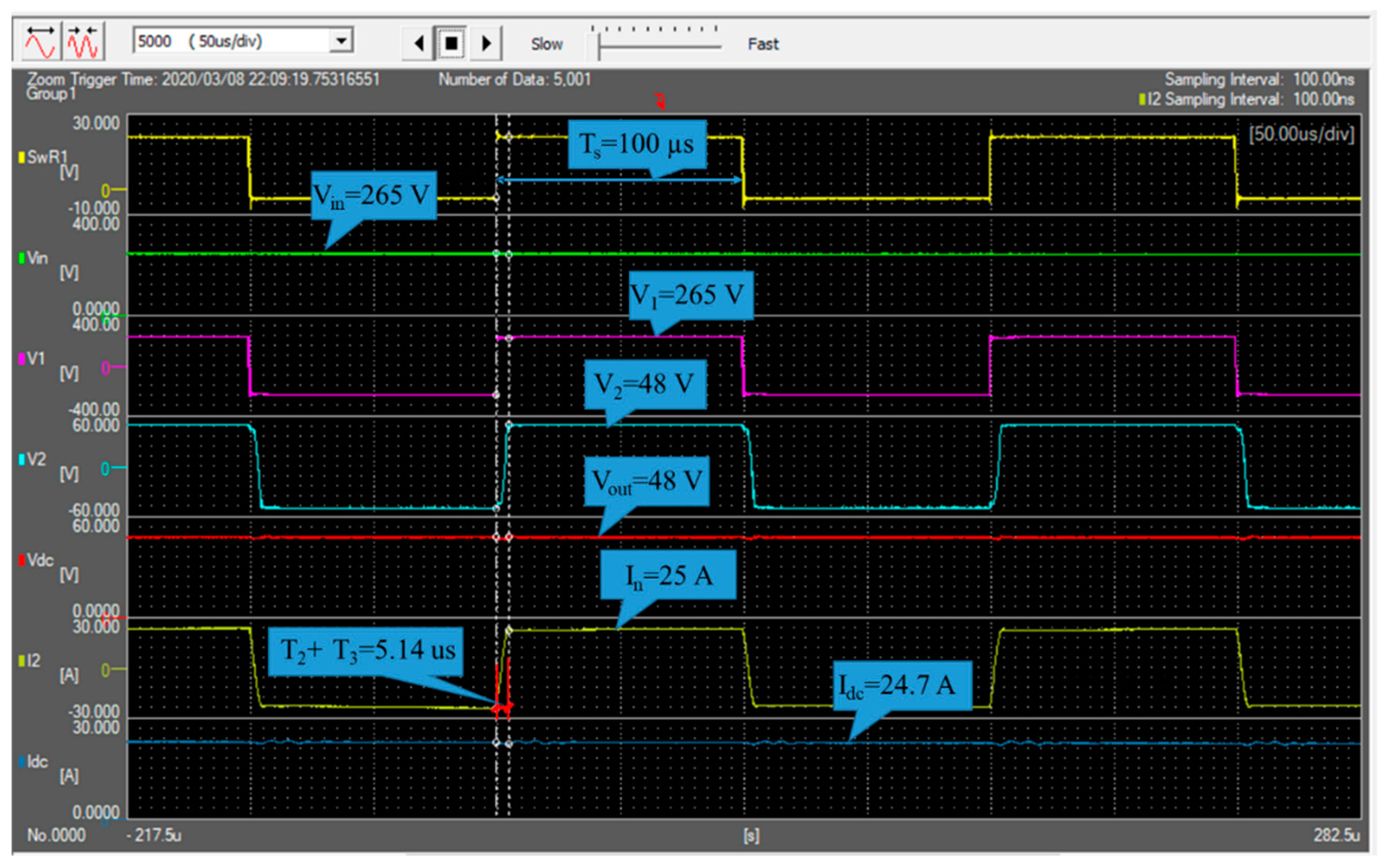
Figure 12 shows the experimental voltage and current waveforms during two and a half periods of the high-frequency transformer at
. The order of the waveforms shown in
Figure 12 is the same as that in
Figure 9. The gate signal
with the half period
= 100 μs generates the primary H-bridge voltage
with the amplitude
= 265 V and switching frequency
= 5 kHz. The secondary rectangular waveform voltage
is observed. The secondary current
flows in the circuit according to the difference in the phase-shift angle between
and
. The amplitude
of the secondary current
is at the designed value of 25 A. The total duration
is obtained, while the duration
= 2 μs of Mode 2–2 in (34) and
= 3.14 μs of Mode 2–3 in (35) are achieved in the same way as in
Figure 9. The average output DC current
is 24.7 A. As can be seen from
Figure 12, a very high TPF experimental value can be achieved in this case for SR–SAB compared to the calculated theoretical value (
TPF = 0.97).
With all the experimental voltage and current waveforms, no high peak stress on the primary and secondary sides is observed as it is in some cases of the normal LC resonant circuit. The overshoot values of primary and secondary voltage in all cases are within the range of 5~10 percent, which is normal, and which is in fact another advantage of this topology because switching devices and capacitors can be selected that are small enough to reduce the overall size.
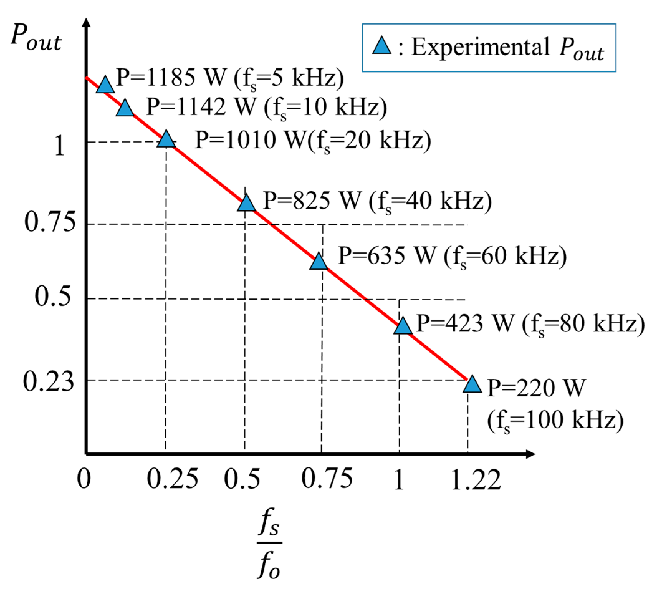
Figure 13 shows the experimental characteristics of the output power
versus the frequency ratio
. When the transformer frequency
varies from 5 kHz to 100 kHz, the output power
gradually decreases from 1185 W to 220 W, and the characteristics coincide with the theoretical linear line in (28). The output power
can be regulated over a wide range by adjusting the frequency ratio
from 0 to 1.22.
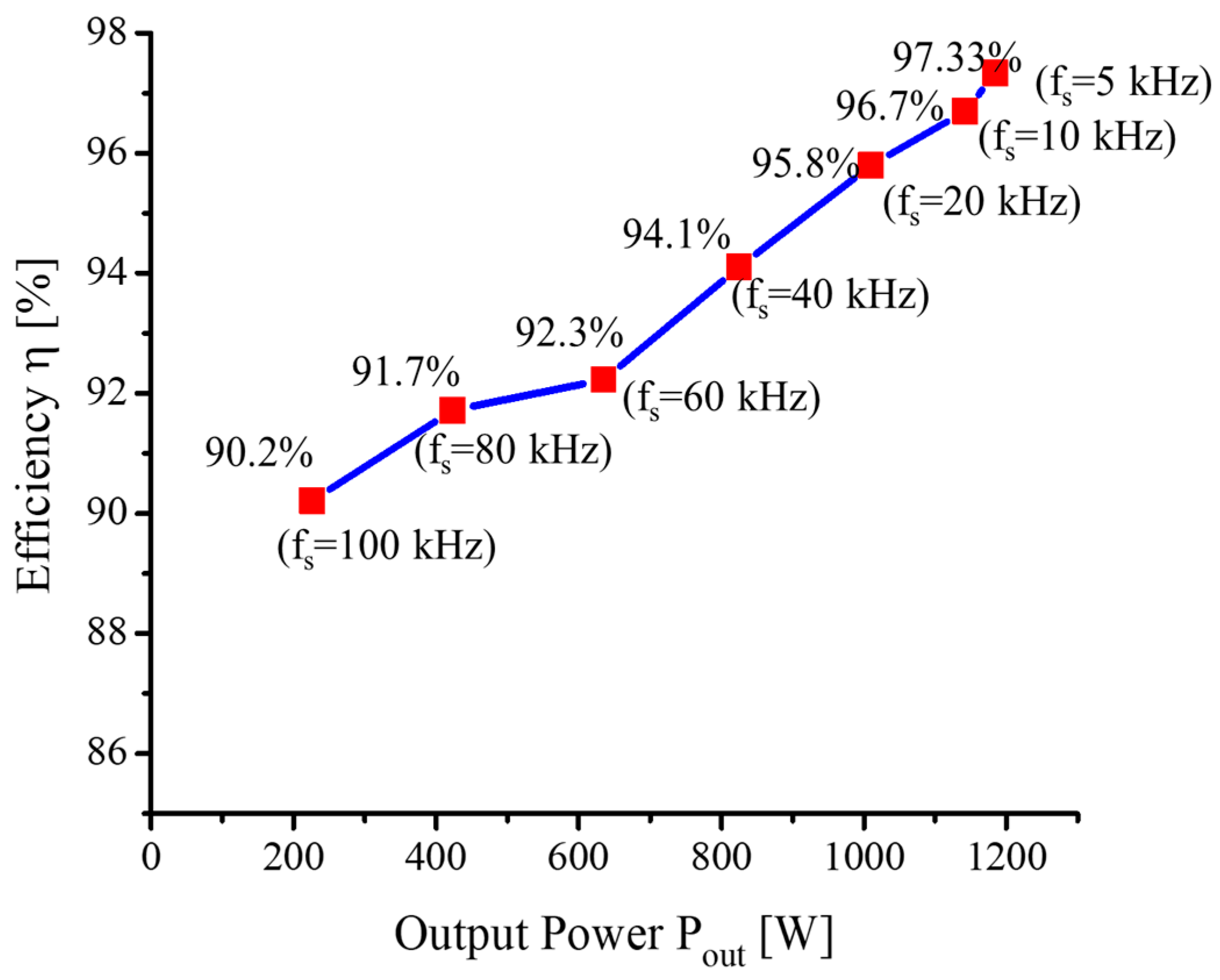
Figure 14 shows the efficiency of the converter for the output power range. The input as well as output electrical powers are both measured using a power analyzer (WT1800, YOKOGAWA). A maximum efficiency of 97.33% is achieved at
with the transformer frequency
. At the rated output power
and the transformer frequency
, the measured efficiency of the circuit is 95.8%. At a low output power
at
, the efficiency is 90.2%. When the transformer frequency
increases from 5 kHz to 100 kHz, the efficiency decreases owing to the reduction in the output power and the increase in the switching loss and iron loss of the transformer with a higher transformer frequency.


