Abstract
This paper investigates the influence of power semiconductor parasitic components on the ground leakage current in the three-phase Current Source Inverter topology, in the literature called H7 or CSI7. This topology allows reducing converter conduction losses with respect to the classic CSI, but at the same time makes the topology more susceptible to the parasitic capacitances of the semiconductors devices. In the present work, a grid-connected converter for photovoltaic power systems is considered as a case study, to investigate the equivalent circuit for ground leakage current. The same analysis can be extended to applications regarding electric drives, since the HF model of electric machines is characterized by stray capacitance between windings and the stator slots/motor frame. Simulation results proved the correctness of the proposed simplified common-mode circuit and highlighted the need of an additional common-mode inductor filter in case of resonance frequencies of the common-mode circuit close to harmonics of the power converter switching frequency. Experimental results are in agreement with the theoretical analysis.
1. Introduction
The exploitation of photovoltaic energy has been a key topic of industrial and academic research in the past decade. The need for a DC/AC conversion for the grid interface has spurred the researchers to investigate the subject from multiple points of view: energy source, power electronics, controls, etc. Nowadays, plants ranging from hundreds of Watts to MW are installed. In this framework, the research for optimized power electronics for small-scale photovoltaic installation has been particularly active [1].
The most widely adopted topology for the DC/AC converters for photovoltaic system is the voltage source inverter (VSI), due to the good efficiency, low component count and the ease of control. However, the presence of electrolytic capacitors which limit the lifetime, the absence of boost capability and short-circuit resilience, has pushed the investigators to study different topologies, including the impedance source converters and the Current Source Inverters (CSI) [2].
The CSI7 converter was first shown in [3]. The basic structure is made of seven reverse-blocking switches in a three-phase configuration. A preliminary analysis of the power devices parasitic capacitances effects was reported in [4]. Follow-up studies were carried out in [5,6], while [7] proposes a new 5-Level CSI topology.
For variable-speed drive application, the CSI has been adopted [8,9] in a back-to-back configuration, where a current source rectifier regulates the input current of a current source inverter driving an induction machine. For PMSM application, the CSI with front-end and LC filter was presented in [10], and a novel control that allows operating without front-end was proposed in [11]. It is important to highlight that the new semiconductor technologies [12] and the advanced electrical machine design strategies [13] increased the applicability of the CSI topologies for some specific applications, for example high-speed high-power density machines for the more electric aircraft [14,15]. Other researchers expanded the CSI research for electric drives analyzing the four-leg [16] operations, the zero voltage switching [17], hybrid PWM strategies [18] or the low switching frequency operations [19].
In a space vector modulation paradigm, there are nine possible vectors (six active and three zero vectors [20]). During the active vector, the output current in the selected phases is equal to the dc inductor current, whereas during the zero vector, the inductor current is free-wheeling within the power electronics. With the CSI7 topology, it is possible to generate the zero vector with only the additional device , disconnecting the dc side from the ac one, with great benefits in terms of ground leakage current [21] and conduction power losses. At the same time, this disconnection makes this topology susceptible to semiconductor parasitic capacitances.
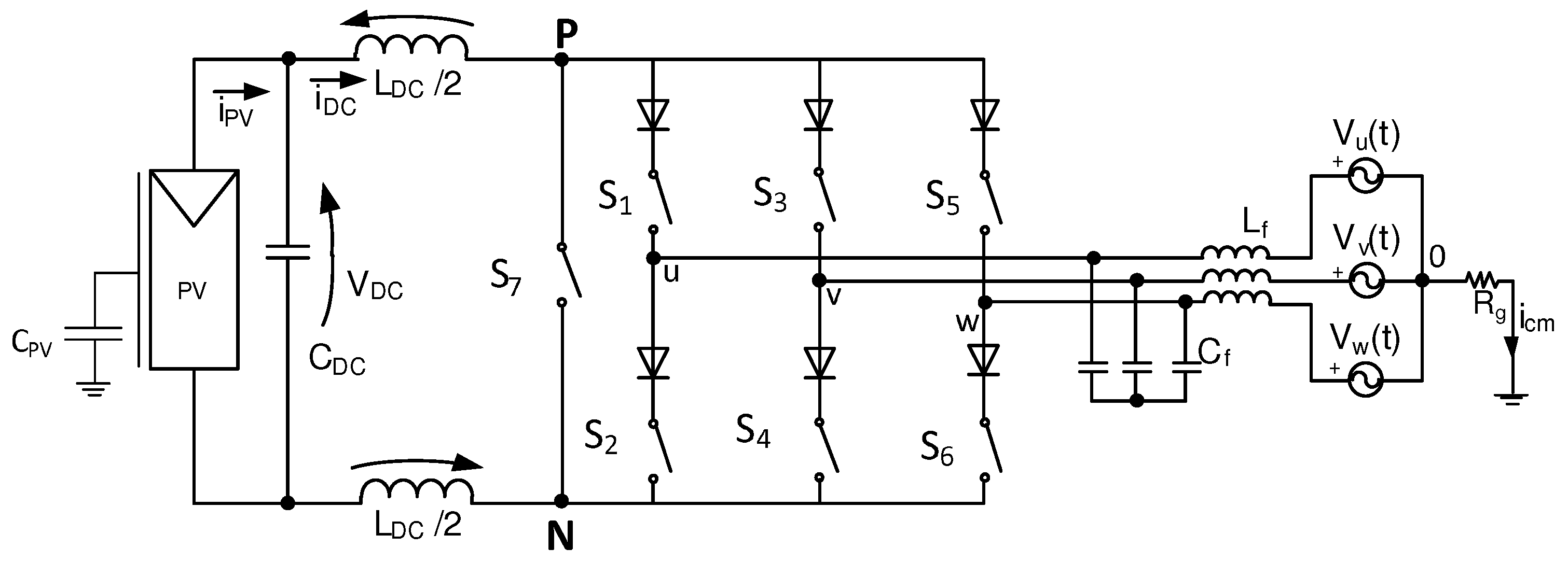
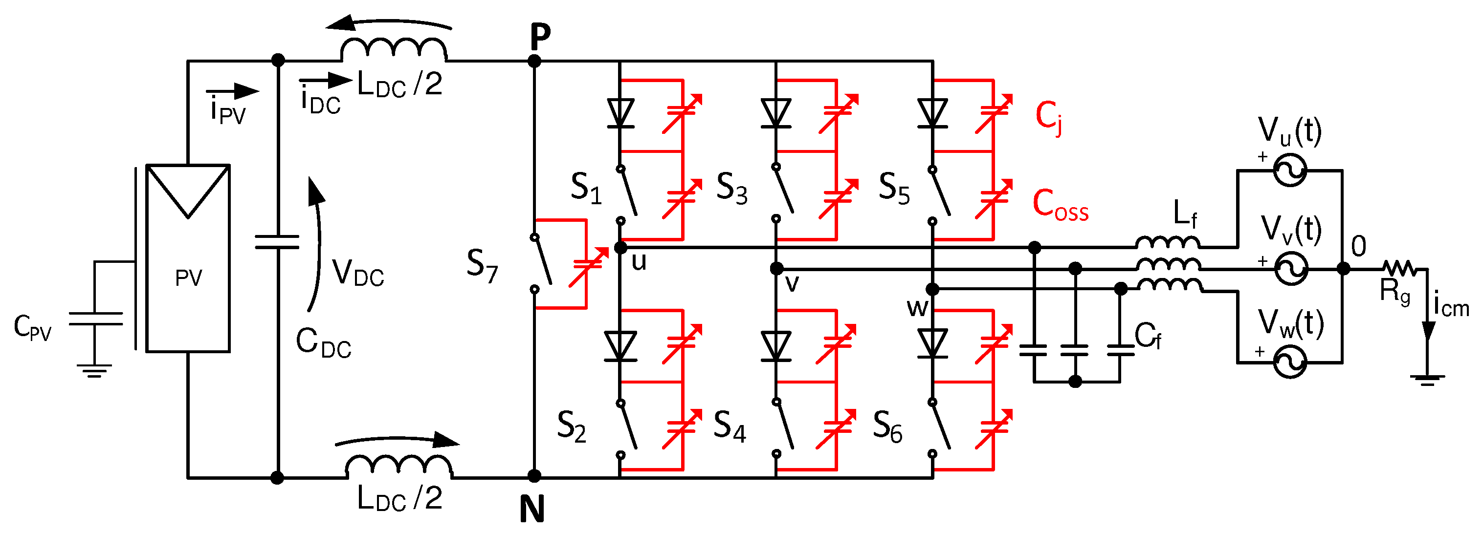
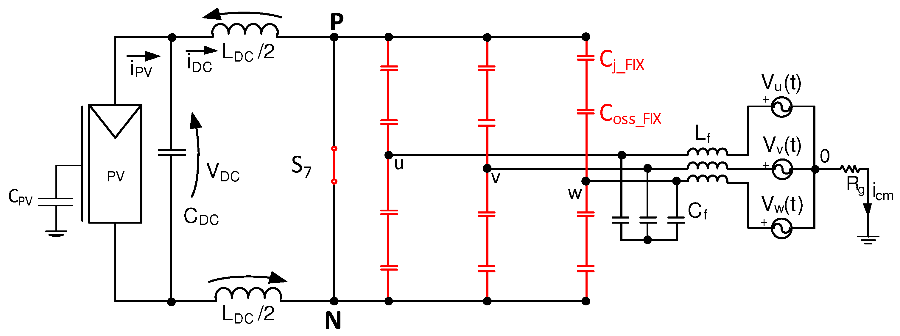
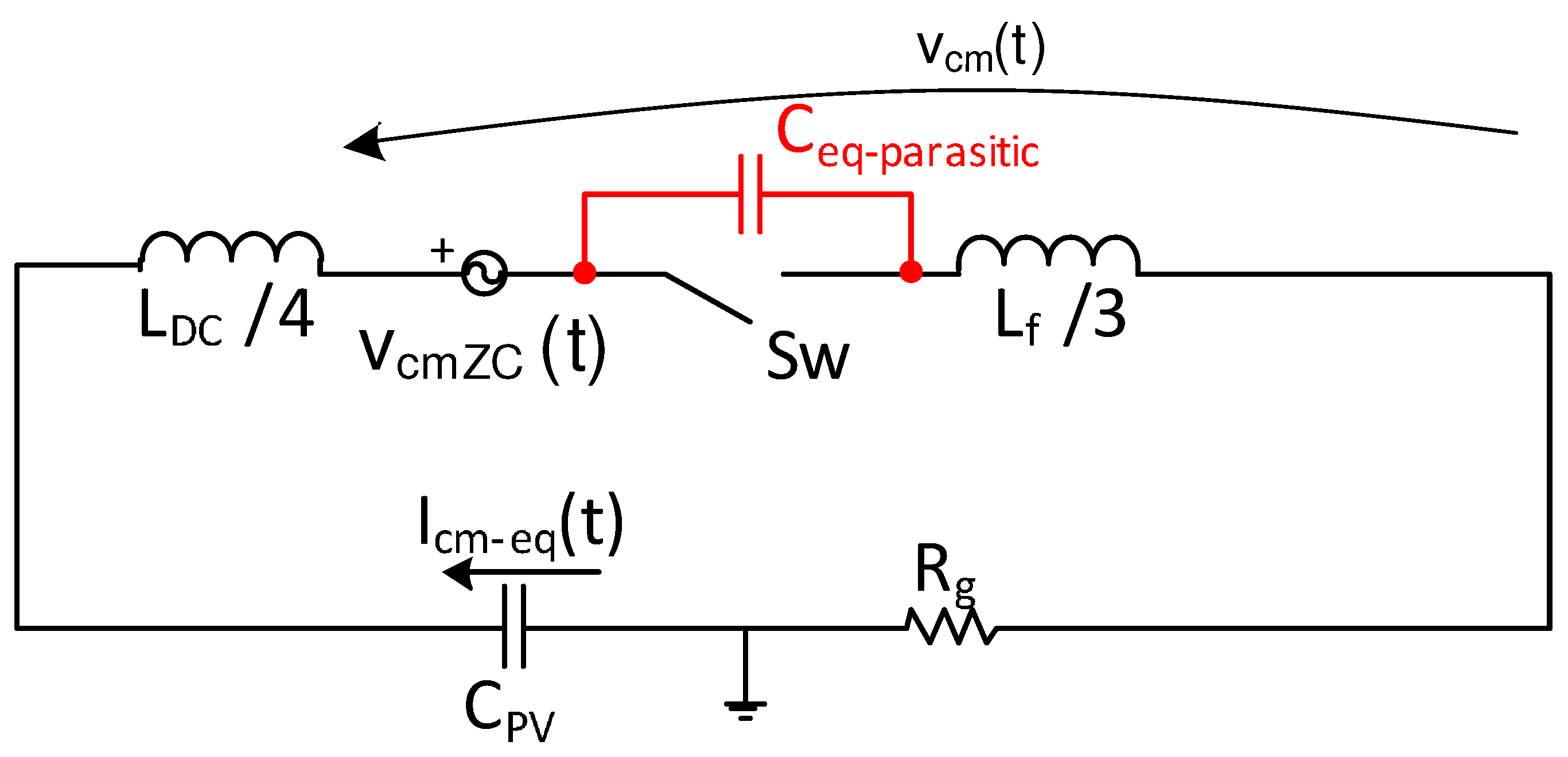
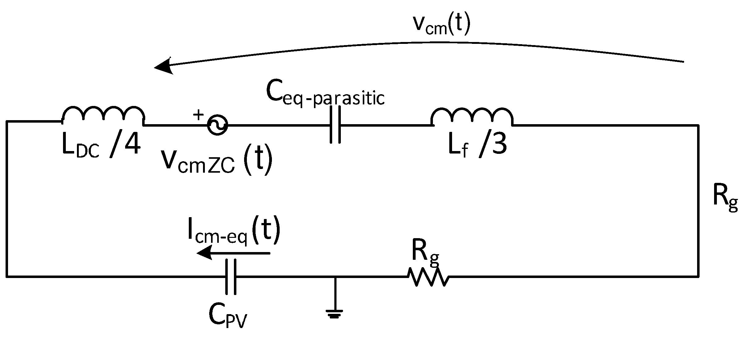
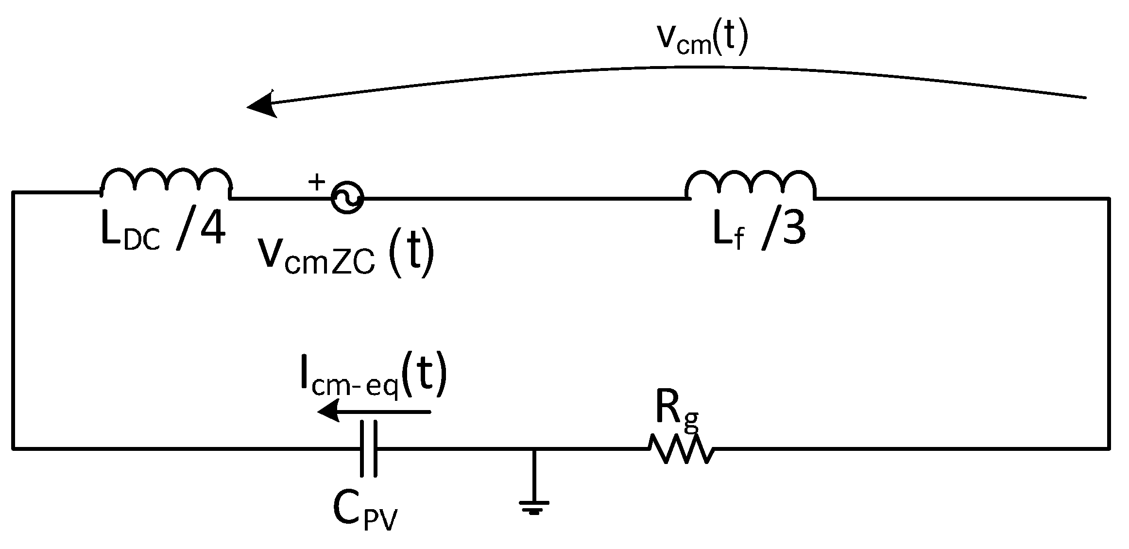
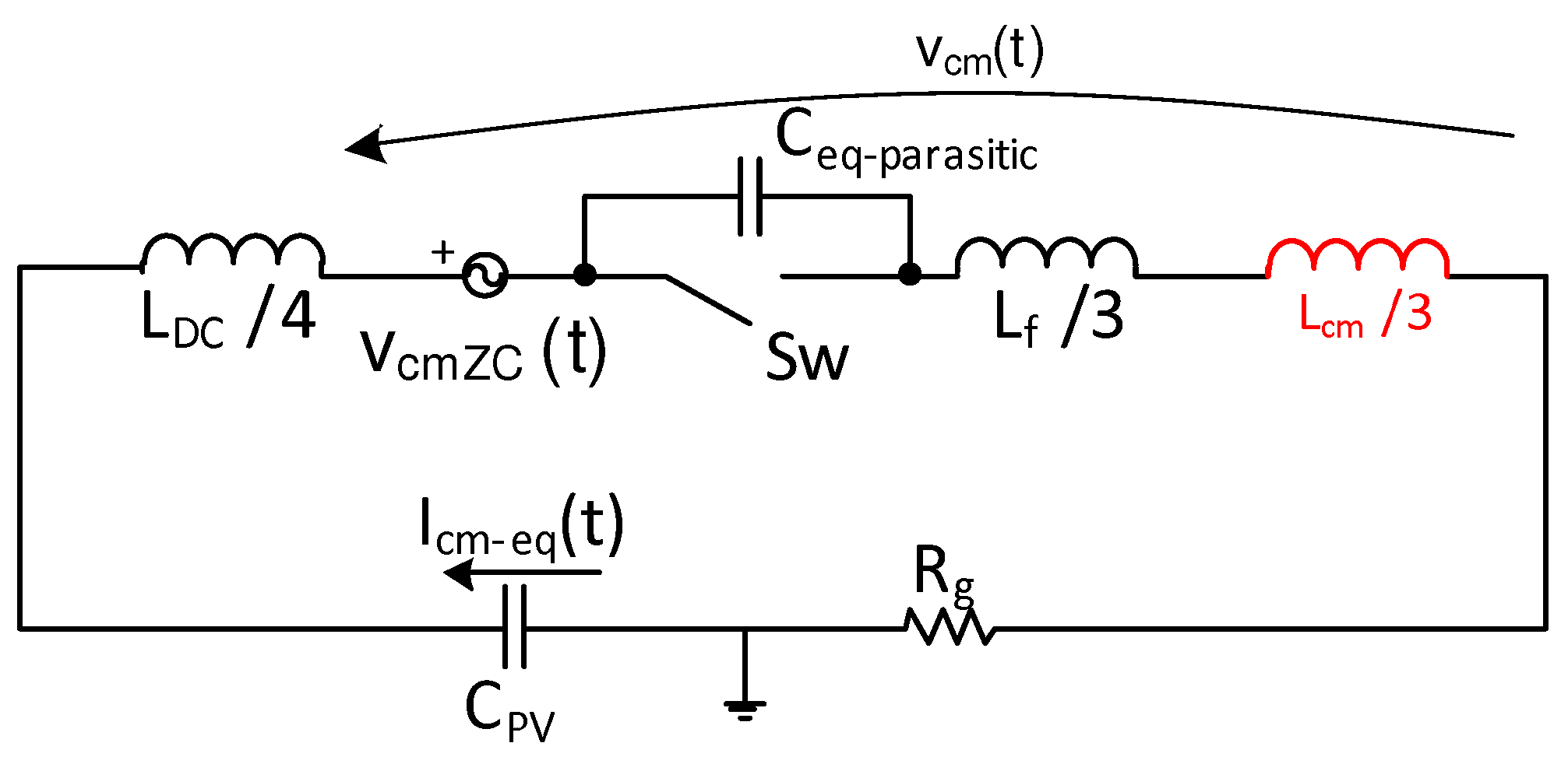
2. Considerations on Parasitic Components
A thorough description and comparison of CSI and CSI7 topologies about output current distortion and semiconductors power losses for transformerless grid-connected converters can be found in [21].
This work has highlighted that the Alternated Space Vector Modulation (see [5]) and the use of split DC input inductors allows obtaining significantly better performance.
In this work, the effect of the parasitic capacitances of the power transistors and diodes is analyzed in terms of ground leakage current. In particular only the output capacitance of the power transistors and the diode junction capacitance was considered.
Figure 1 and Figure 2 show the schematic of a CSI7 topology with and without the aforementioned parasitic capacitances.
Figure 1.
Schematic of CSI7 topology.
Figure 2.
CSI7 topology with parasitic capacitors.
Photovoltaic plants are particularly prone to ground leakage current issues, since the PV modules exhibit a large stray capacitance with respect to grounded metallic structures that are part of the installation. The analysis and the equivalent CM circuit of the converter developed in the present work can be usefully extended to electric drives as well, since the DC source that replaces the PV modules is fitted with capacitors to ground for EMI suppression and the HF model of electric machines is also characterized by stray capacitance between the machine windings and the stator slots/motor frame, [22,23].
The value of the power semiconductor’s parasitic capacitance is not constant, but decreases when the Drain-Source voltage and Diode Reverse Voltage increases. The analysis was carried out considering SiC MOSFETs (C2M0025120D) and Diode (FFSH50120A). Figure 3 shows the parasitic capacitances evolution voltage depending.
Figure 3.
and variations for SiC MOSFETs (C2M0025120D) and Diode (FFSH50120A).
To allow fast simulations, constant values of and could be taken into consideration, namely and . This assumption allows simplifying the analysis of the ground leakage current and will be validated by means of numerical simulations in Section 3. The choice of the fixed values is not an easy task. In the simulation section the minimum capacitance values were chosen, i.e., the capacitance value when the maximum voltage applied by the grid is present across them.
Since one of the goals of this work is to propose an equivalent common-mode circuit which integrates the semiconductor parasitic capacitances, it is important to focus on the power converter configuration during Zero Vector application. In fact, in this condition there is no connection between the DC link and the grid in the case of ideal switches.
Figure 4 shows the simplified configuration during Zero Vector application ( ON and – OFF). During the application of any Active vectors the effect of the parasitic capacitances is null in terms of ground leakage current.
Figure 4.
CSI7 topology in the case of Zero Vector applications with power devices parasitic capacitors.
In Current Source Inverter topologies, the common-mode voltage can be calculated using the star point of the three-phase grid voltage as voltage reference [24]:
The variable was defined in [25] and represents the voltage in case of zero . The instantaneous value of (the same consideration is true for ) shows a noticeable difference if the parasitic capacitance is considered.
Figure 5 shows the sequence of Alternated space vector modulation and the evolution of during a sampling period : and represent the time intervals of Active Vectors while represents the time interval of the Zero Vector application as described in [5]. In the same figure, the blue square represents the area of the allowed values for during the Zero Vector application, due to the presence of the power devices parasitic capacitances.
Figure 5.
Evolution of (lower trace in blue) during a switching period in case of ASVM (active vectors during and , zero vector during ). evolution with ideal power devices in black trace, and with real power devices in red trace.
During the Zero Vector, i.e., during , the instantaneous value is not equal to zero (as in case of simulations with ideal switches), but its value depends on the circuit, which is obviously modified by the addition of the capacitance.
An additional equivalent parasitic capacitance can be simply added to the CSI7 common-mode circuit obtained with ideal switches [25].
Figure 6 shows the circuit considering the capacitance of the switches: during the active vectors, the capacitance is shorted by the switches.
Figure 6.
Equivalent common-mode circuit considering parasitic capacitors.
Starting from Figure 4 the value of can be simply computed as the parallel of six capacitors equal to the series of and . The correctness of this last common-mode circuit will be verified in the following section.
Figure 7 shows the equivalent common mode circuit when a Zero Vector is applied, while Figure 8 shows the equivalent circuit in the case of Active Vector application. From these two circuits it is possible highlights the two resonant frequencies present in the equivalent common-mode circuit.
Figure 7.
Equivalent common mode circuit in Zero state condition.
Figure 8.
Equivalent common mode circuit in Active state condition.
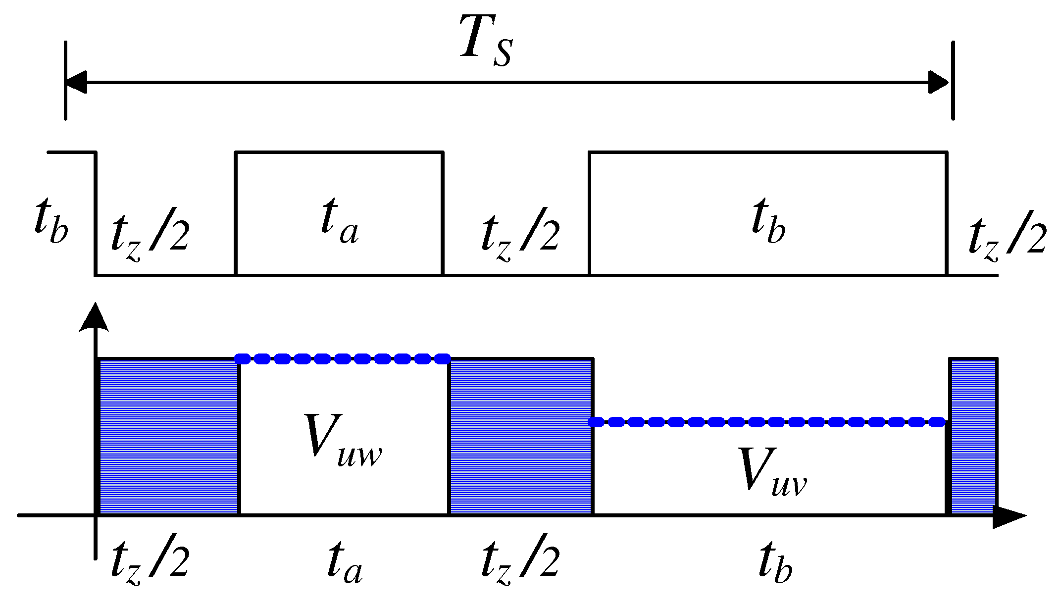
3. Numerical Simulations
In this section, the behavior of CSI7 with the presence of parasitic capacitances and is analyzed in MATLAB and PLECS environments. Table 1 summarizes the simulation and experimental parameters.
Table 1.
Simulation parameters.
3.1. Matching between Variable and Fixed Capacitances
With the aforementioned parameters, the first step is to identify the equivalence between a variable output capacitor in Figure 2 and a fixed equivalent capacitor in Figure 4. The worst condition in terms of energy is represented during the maximum voltage across the capacitors (in this case, the output capacitance is equal to the minimum one).
This is an approximation able to simplify the analysis of the ground leakage current.
Figure 9 shows the waveform of the in case of variable (blue line) and fixed parasitic capacitance (dashed red line) values. It can be noted that this approximation introduces a good match despite some natural differences due to the variable resonance frequency obtained when and are taken into account, however the RMS value with fixed parasitic capacitance is very close as reported in Table 2.
Figure 9.
Comparison between (blue line) and (dashed red line) with and .
Table 2.
RMS values of in case of variable and fixed value of parasitic capacitance.
This approximation offers a good trade off to compute the RMS value with an easier simulation. For safety reasons, it is important to keep into consideration that the RMS value of the current is most important with respect to the harmonic content.
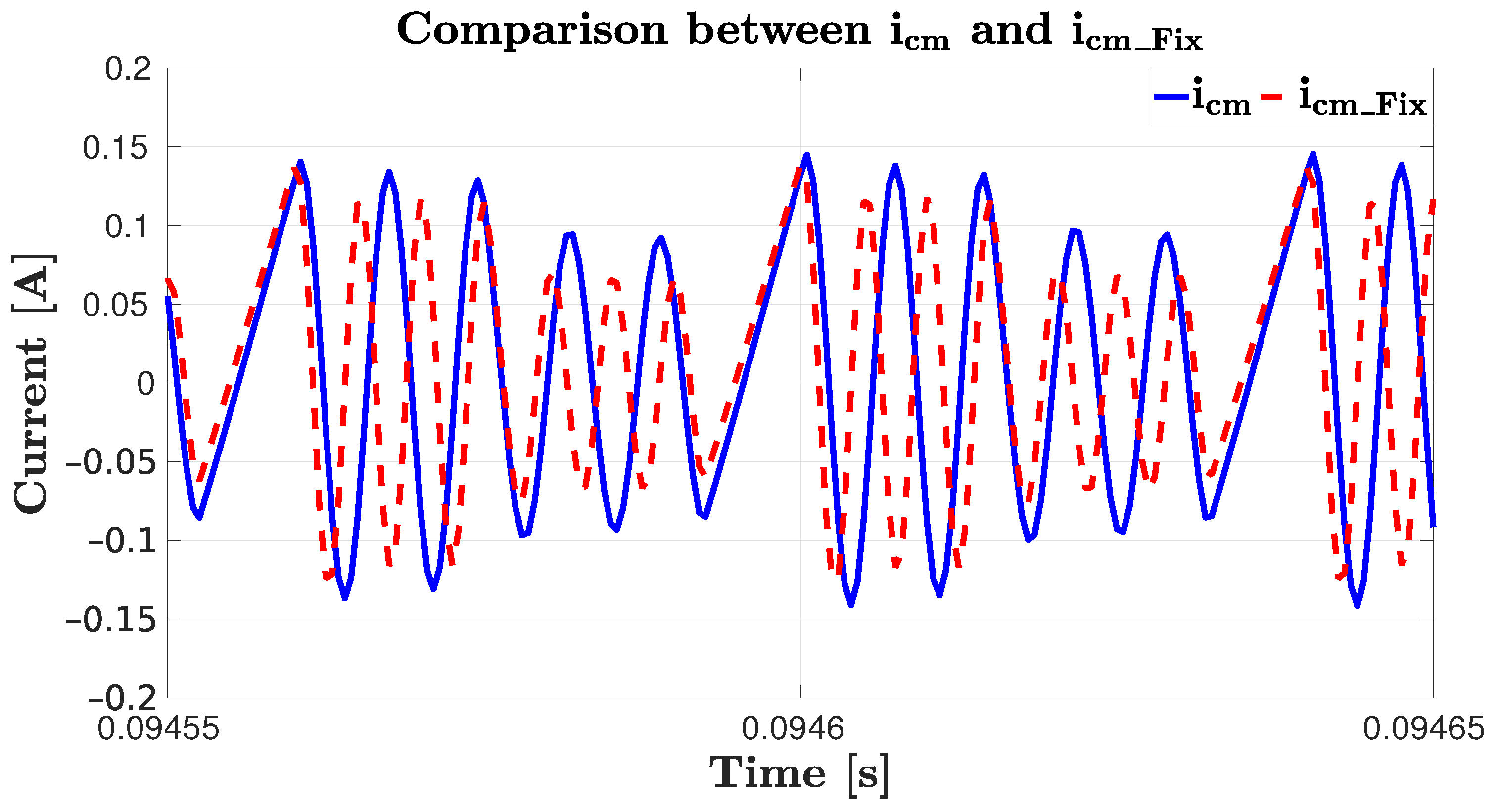
3.2. Validation of the Equivalent Common-Mode Circuit
With the previous assumptions, the following simulations will take into account fixed values of and (considering the minimum one).
By analyzing Figure 6, it can be noted that for each state a different resonant circuit is obtained, see Figure 7 and Figure 8.
Figure 10 shows the different behavior of the current (blue line) depending on the output vector of the converter, transitioning between the Zero and the Active Vectors (dotted red line). When an Active Vector is applied, it is worth noticing that varies, together with the oscillation frequency: this is consistent with the change of the resonance frequency of the common-mode circuit. When an Active Vector is applied, the common-mode equivalent circuit varies, since is short-circuited.
Figure 10.
(blue line) evolution during Zero and Active Vectors. The zero value of the red trace represents the Zero Vector while the value 1 represents the application of any Active Vectors.
This is also apparent in Figure 11 where the dependency of (blue line) on Zero and Active Vectors (dotted red line) is shown. When a Zero Vector is applied, value remains constant, in accordance with the expected behavior from theory.
Figure 11.
evolution in case of Zero Vector (State 0) and any Active Vectors (State 1).
The Bode diagram of the transfer function is reported in Figure 12 for the equivalent common mode circuits in Figure 7 (blue line) and Figure 8 (red line).
Figure 12.
Bode diagram for Zero (blue) and Active (red) Vectors.
The resonance frequencies of the equivalent circuit are located before the switching frequency (in case of Active Vector) and near the 8th harmonic of the switching frequency (in case of Zero Vector).
This particular situation can have a strong impact on the waveform of . In fact, in the equivalent circuit the resonance frequency of the Zero Vector matches the 8th harmonic of the switching frequency.
The correctness of the equivalent circuit of Figure 6 using power semiconductors models with constant parasitic capacitances is assessed in Figure 13 that puts in evidence the strong similarity between (blue line) and (dashed red line).
Figure 13.
Comparison between (blue line) and (dashed red line) with fixed capacitances.
In particular, it compares the , determined considering the entire power converter system shown in Figure 2 with fixed values of and , and calculated according to the equivalent circuit of Figure 6. The waveform of is obtained by means of simulation of the whole power converter system considering an open circuit path, instead of .
The simulation reports a good match between and even in the presence of parasitic capacitances on power semiconductors as already shown in the first step of simulations.
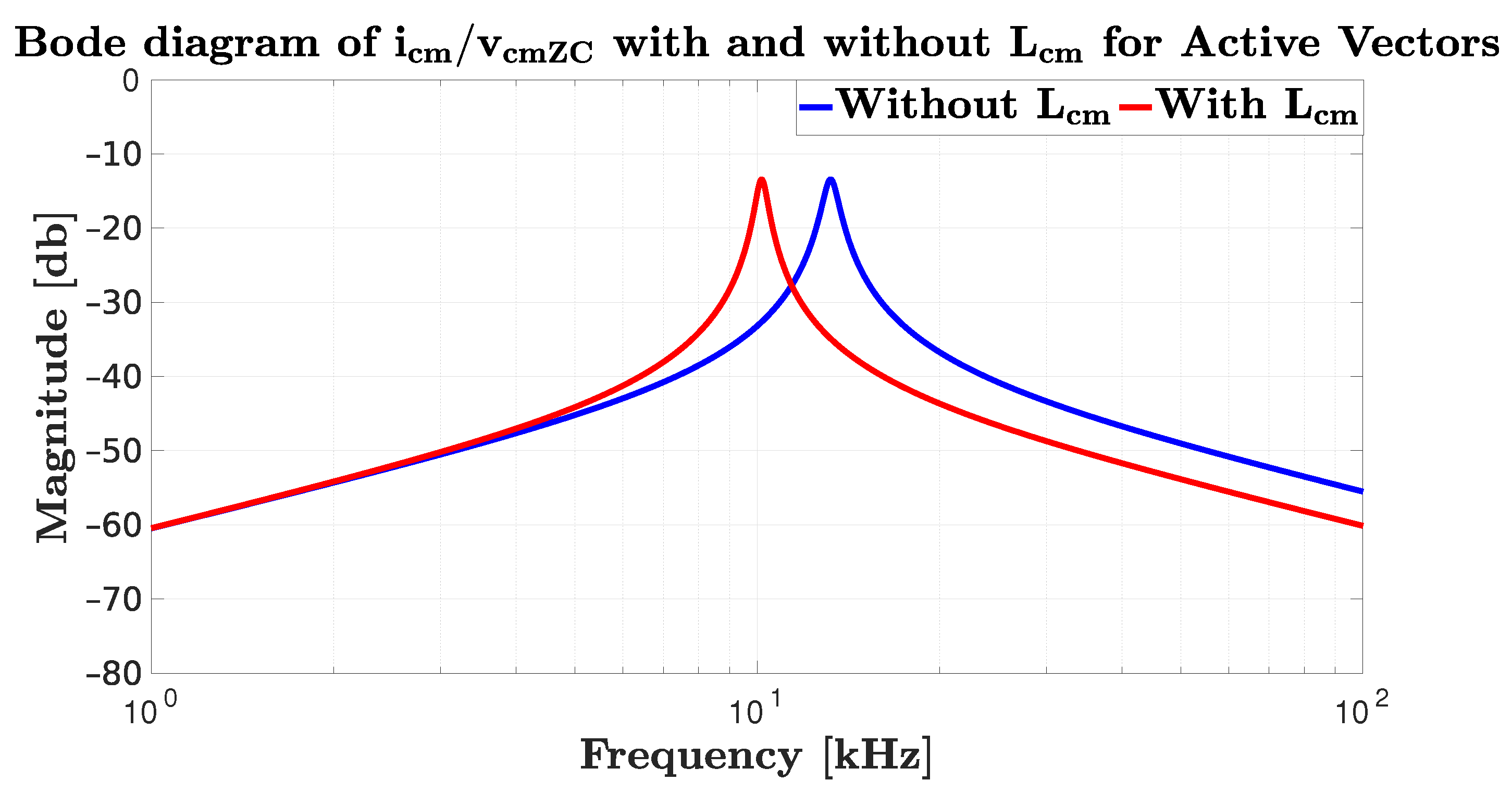
3.3. Critical Aspects of the Resonant Frequency
In the following simulations constant values of (defined as the series connection between and for every single switch) will be considered, namely , , and . That bigger values consider other parasitic capacitance introduced by PCB, connections, etc.
The purpose of this simulation is to put in evidence the drawback introduced when the resonance frequency match exactly a harmonic of the switching frequency.
Figure 14 and Figure 15 summarizes the waveforms of and their Fast Fourier Transform (FFT) obtained by varying the equivalent parasitic capacitance . These figures confirm that is not influenced at all by the value of the semiconductor parasitic capacitance. Conversely, the ground leakage current is heavily affected. Figure 16 and Figure 17 report the waveforms and spectra of , while RMS values of the currents are summarized in Table 3. Considering the obtained results, the worst case scenario is related to . As previously mentioned, the reason lies in the different resonance frequency of the common-mode circuit. In fact, the resonance frequency response that happens during the Zero vector of results equal to , as reported also in Figure 18 Bode diagram. The resulting resonance frequency exactly matches the fourth switching frequency harmonic, thus determining high values. This is yet another example of the importance of the resonance frequency in the response of the equivalent common-mode circuit in practical implementations.
Figure 14.
Waveforms of with different values of .
Figure 15.
FFT of with different values of .
Figure 16.
Waveforms of with different values of .
Figure 17.
FFT of with different values of .
Table 3.
RMS values of the currents.
Figure 18.
Bode Diagram of during Zero Vector application with different values of .
3.4. Mitigation of the Resonance Problem
If the value of , during the Zero Vector application, results in a resonance frequency of the common-mode circuit that is close to one of the harmonics of the switching frequency, a small output common mode choke can be added at the converter output to modify the resonance frequency.
The equivalent common-mode circuit shown in Figure 6 is modified into the one shown in Figure 19 by introducing the common mode choke converter output, thus changing the resonance frequency, as shown in Figure 20 in case of .
Figure 19.
Equivalent common mode circuit with Common mode Filter.
Figure 20.
Bode Diagram of with different values of and .
According to Figure 20 the RMS value of increases with because the higher is, the lower is the resulting the attenuation of the switching frequency components. Table 4 summarizes the RMS of with the presence of .
Table 4.
RMS values of with .
Figure 21 shows the Bode diagram of during Active Vector application with and without , putting in evidence the shift of the resonance frequency with and without the . As shown by Figure 6 and Figure 19 the switch is closed during Active Vectors, so does not influence the behavior during an Active Vector application.
Figure 21.
Bode Diagram of with and without during Active Vectors application.
By employing an additional the resonance frequency can be further decreased: in this particular example, it drops to , a value that is far lower than the fundamental switching frequency .
As can be seen in Figure 10, the attenuation of is higher during Active Vector time intervals.
The presence of parasitic semiconductor capacitances affected strongly the common-mode current, and to a much lesser extent the efficiency of the converter. Semiconductor power losses computations in case of null parasitic capacitances or with the aforementioned values do not provide significant variations. For that reason, semiconductor power losses results were not shown in this work. The computation of these last ones in case of a different number of PV panels, in standard CSI and CSI7 topology were analyzed in detail in [21].
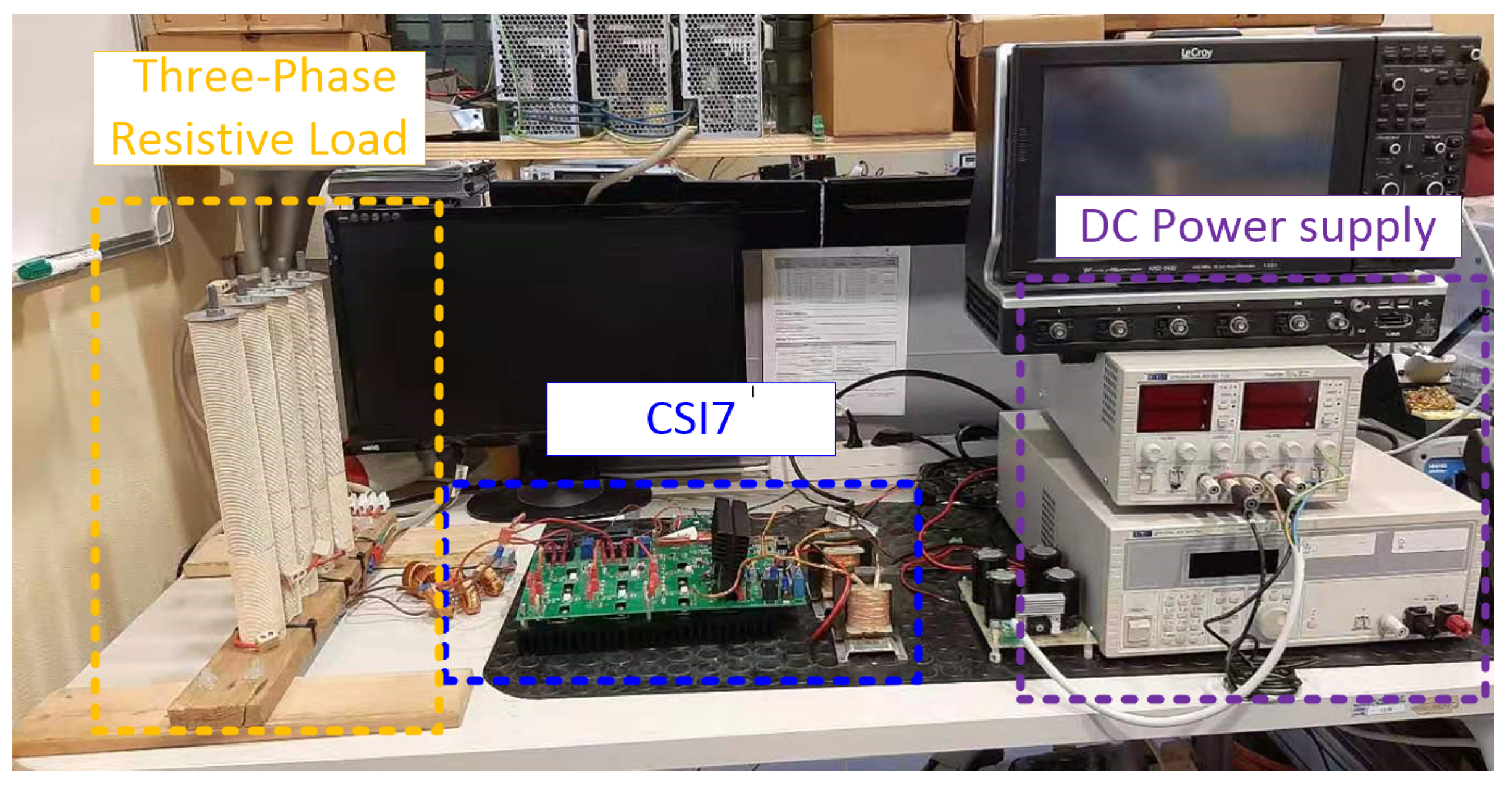
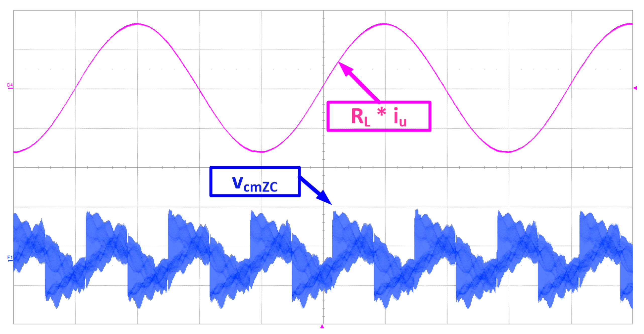
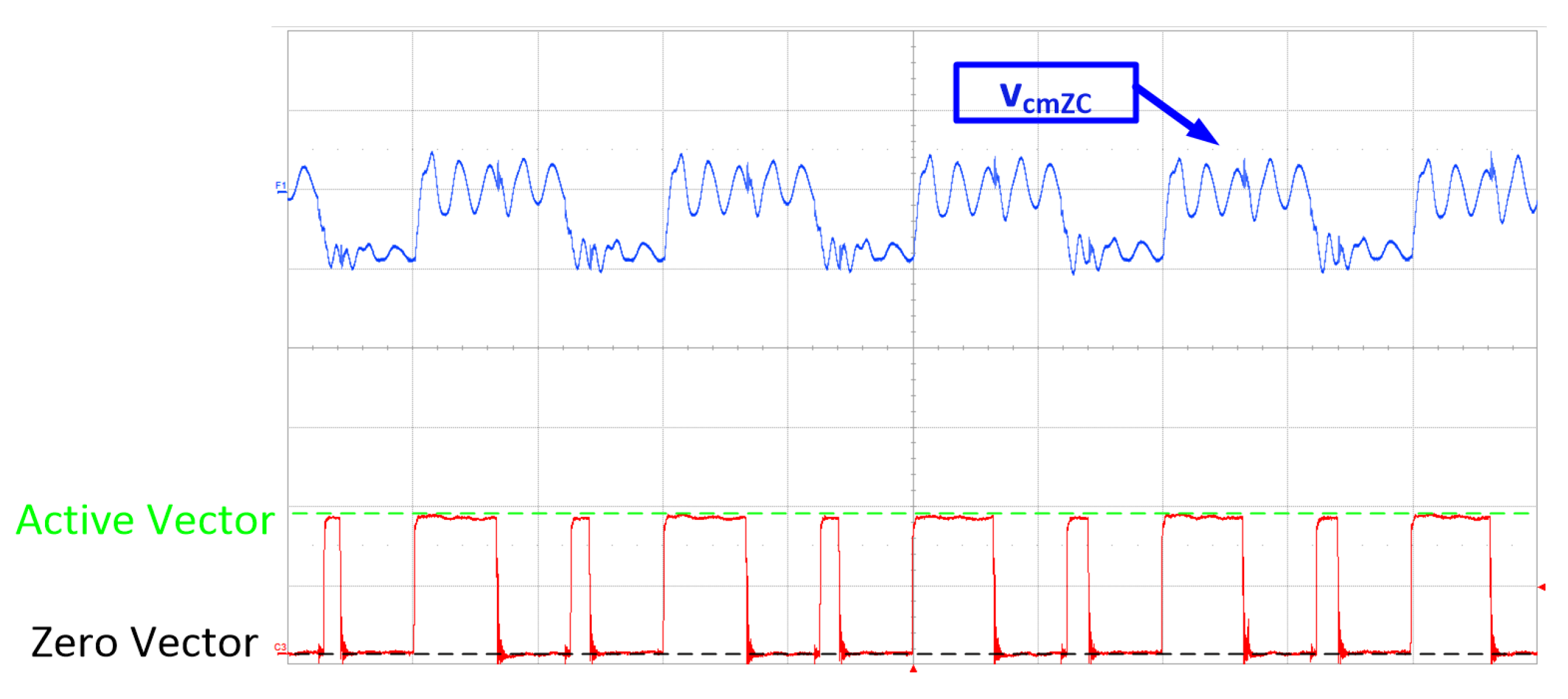
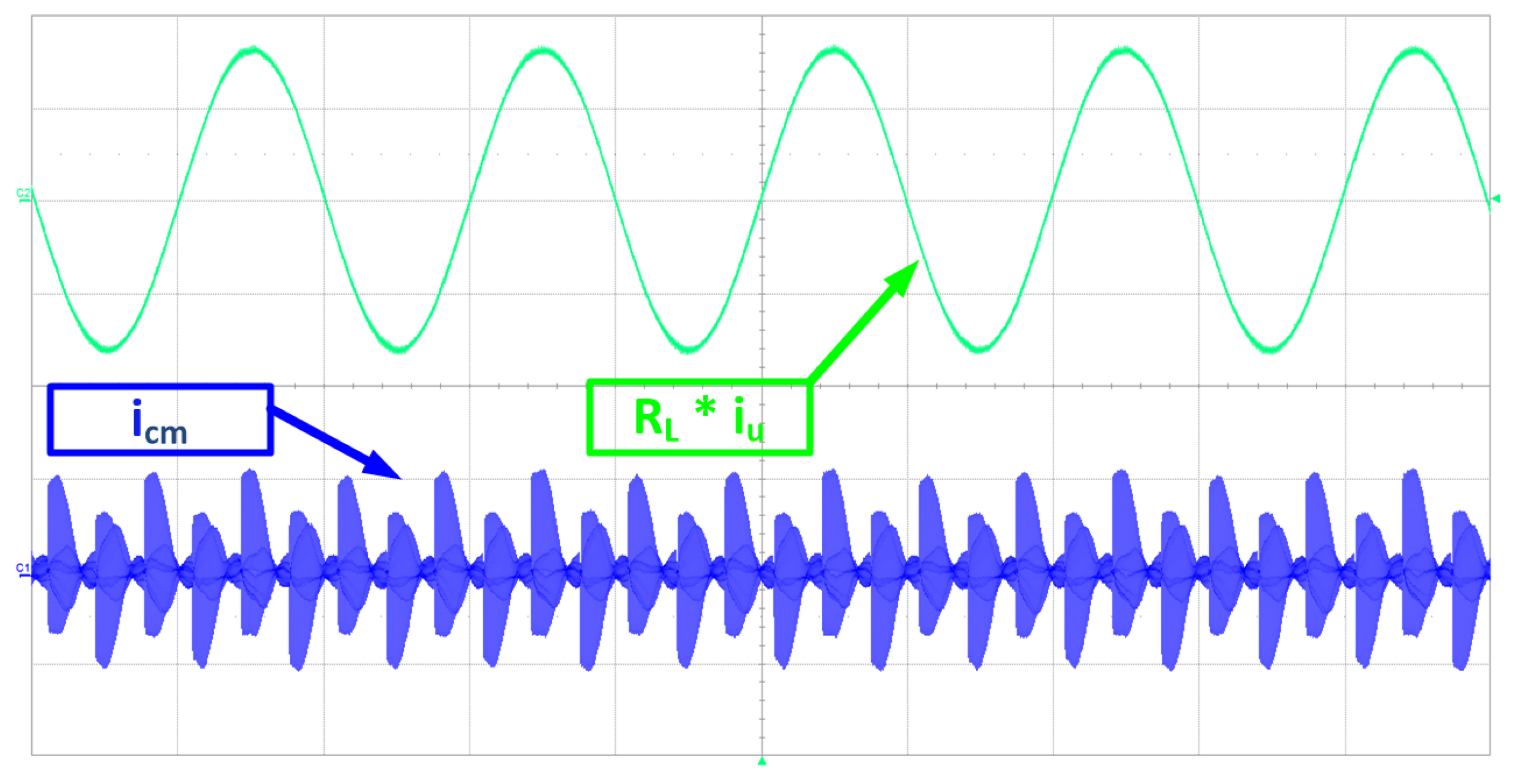
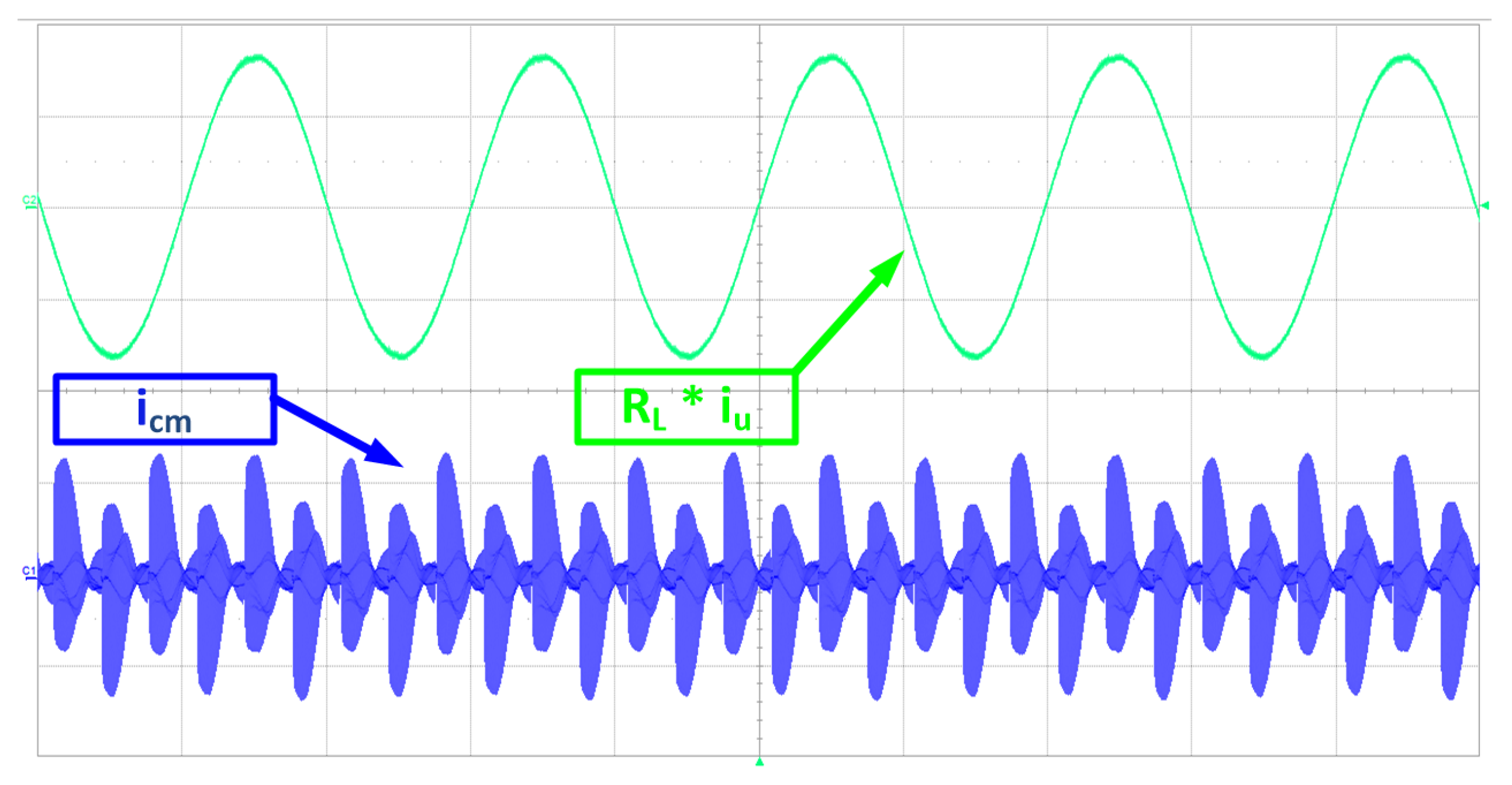
4. Experimental Results
The test setup, shown in Figure 22, comprising a prototype power converter, was used for experimental validation.
Figure 22.
Picture of CSI7 power converter experimental setup.
The experiments are performed in an island operation with the converter connected to a ohmic load () with the parameters listed in Table 1.
Figure 23 shows the schematic of the experimental test bench, where a Hall effect current sensor was used to measure the current that flows through the series of and .
Figure 23.
Schematic of the experimental test bench.
A power supply with voltage = is connected to the DC link and is chosen as current reference to achieve an AC voltage of = (reported in Figure 24).
Figure 24.
Experimental waveforms. (upper trace, ), (lower trace, ). The time division is .
It can be noted from Figure 25 that changes depend on the Active Vector but are constant during the Zero Vector (keeping its previous value), as expected by the theoretical analysis (Figure 11). More oscillations appear due to the stray inductance of the power converter.
Figure 25.
Experimental waveforms. (upper trace, ) and States (lower trace). The time division is .
Figure 26 and Figure 27 show the evolution of without and with the connection of a capacitor in parallel to every reverse-blocking switch.
Figure 26.
Experimental waveforms. (upper trace, ), (lower trace, ). The time division is .
Figure 27.
Experimental waveforms. (upper trace, ), (lower trace, ). The time division is .
In accordance with the theory, changes significantly, confirming the dependence on the parasitic capacitance. Increasing the capacitance leads to an increase of increases from to .
5. Conclusions
In this work the effect of the power device parasitic capacitances on ground leakage current was investigated in case of the CSI7 topology. Simulations and experiments show that the effect of device parasitic capacitances have a great impact on the behavior of CSI topologies that ideally present a separation between the DC source and the AC grid during the zero vector application. The same effect can be observed in case of VSI topologies that present an isolation from DC source to AC grid during certain time intervals of the switching period. Simulation results have proven the correctness of the equivalent common-mode circuit in predicting the two resonance frequencies during active and zero vector applications. In a practical implementation, taking into account real power semiconductor devices greatly impacts the ground leakage current. The critical issue is that different parasitic capacitance values of the power transistors can change greatly the resonance frequency values of the common-mode circuit. This work shows that if these resonance frequencies are close to harmonics of the switching frequency of the power converter, the ground leakage current (i.e., the common-mode current) greatly arises. To avoid the matching of these frequencies, thus reducing ground leakage current, an additional common-mode inductor should be added to change resonance frequencies values.
Author Contributions
Conceptualization, G.M. and E.L.; Data curation, G.M. and E.C.; Formal analysis, F.I. and E.L.; Investigation, G.M.; Methodology, G.B. and E.L.; Project administration, G.B.; Validation, F.I. and G.B.; Writing—original draft, G.M. and E.C.; Writing—review and editing, E.C., G.B., F.I. and E.L. All authors have read and agreed to the published version of the manuscript.
Funding
This work is supported by Ministry of Science & Technology under National Key R&D Program of China, under Grant 2021YFE0108600.
Institutional Review Board Statement
Not applicable.
Informed Consent Statement
Not applicable.
Data Availability Statement
Data sharing not applicable.
Conflicts of Interest
The authors declare no conflict of interest.
References
- Kjaer, S.B.; Pedersen, J.K.; Blaabjerg, F. A Review of Single-Phase Grid-Connected Inverters for Photovoltaic Modules. IEEE Trans. Ind. Appl. 2005, 41, 1292–1306. [Google Scholar] [CrossRef]
- Sahan, B.; Vergara, A.N.; Henze, N.; Engler, A.; Zacharias, P. A Single-Stage PV Module Integrated Converter Based on a Low-Power Current-Source Inverter. IEEE Trans. Ind. Electron. 2008, 55, 2602–2609. [Google Scholar] [CrossRef]
- Bendre, A.; Wallace, I.; Nord, J.; Venkataramanan, G. A Current Source PWM Inverter with Actively Commutated SCRs. IEEE Trans. Power Electron. 2002, 17, 461–468. [Google Scholar] [CrossRef]
- Migliazza, G.; Carfagna, E.; Bernardi, F.; Lorenzani, E. Ground Leakage Current in Three-Phase Current Source Inverters Depending on Power Semiconductors Parasitic Capacitances. In Proceedings of the 2020 IEEE Energy Conversion Congress and Exposition (ECCE), Detroit, MI, USA, 11–15 October 2020; pp. 2125–2130. [Google Scholar] [CrossRef]
- Lorenzani, E.; Immovilli, F.; Migliazza, G.; Frigieri, M.; Bianchini, C.; Davoli, M. CSI7: A Modified Three-Phase Current-Source Inverter for Modular Photovoltaic Applications. IEEE Trans. Ind. Electron. 2017, 64, 5449–5459. [Google Scholar] [CrossRef]
- Wang, W.; Gao, F.; Yang, Y.; Blaabjerg, F. Operation and Modulation of H7 Current-Source Inverter With Hybrid SiC and Si Semiconductor Switches. IEEE J. Emerg. Sel. Top. Power Electron. 2018, 6, 387–399. [Google Scholar] [CrossRef]
- Gao, F.; Loh, P.C.; Blaabjerg, F.; Vilathgamuwa, D.M. Five-Level Current-Source Inverters With Buck–Boost and Inductive-Current Balancing Capabilities. IEEE Trans. Ind. Electron. 2010, 57, 2613–2622. [Google Scholar] [CrossRef]
- Espinoza, J.R.; Joos, G. A Current-Source-Inverter-Fed Induction Motor Drive System with Reduced Losses. IEEE Trans. Ind. Appl. 1998, 34, 796–805. [Google Scholar] [CrossRef]
- Li, Y.W.; Pande, M.; Zargari, N.R.; Wu, B. DC-Link Current Minimization for High-Power Current-Source Motor Drives. IEEE Trans. Power Electron. 2009, 24, 232–240. [Google Scholar]
- Lee, H.; Jung, S.; Sul, S. A Current Controller Design for Current Source Inverter-Fed AC Machine Drive System. IEEE Trans. Power Electron. 2013, 28, 1366–1381. [Google Scholar] [CrossRef]
- Migliazza, G.; Buticchi, G.; Carfagna, E.; Lorenzani, E.; Madonna, V.; Giangrande, P.; Galea, M. DC Current Control for a Single-Stage Current Source Inverter in Motor Drive Application. IEEE Trans. Power Electron. 2021, 36, 3367–3376. [Google Scholar] [CrossRef]
- Morya, A.K.; Gardner, M.C.; Anvari, B.; Liu, L.; Yepes, A.G.; Doval-Gandoy, J.; Toliyat, H.A. Wide Bandgap Devices in AC Electric Drives: Opportunities and Challenges. IEEE Trans. Transp. Electrif. 2019, 5, 3–20. [Google Scholar] [CrossRef]
- Shen, J.; Qin, X.; Wang, Y. High-Speed Permanent Magnet Electrical Machines—Applications, Key Issues and Challenges. CES Trans. Electr. Mach. Syst. 2018, 2, 23–33. [Google Scholar] [CrossRef]
- Buticchi, G.; Bozhko, S.; Liserre, M.; Wheeler, P.; Al-Haddad, K. On-Board Microgrids for the More Electric Aircraft—Technology Review. IEEE Trans. Ind. Electron. 2019, 66, 5588–5599. [Google Scholar] [CrossRef] [Green Version]
- Madonna, V.; Migliazza, G.; Giangrande, P.; Lorenzani, E.; Buticchi, G.; Galea, M. The Rebirth of the Current Source Inverter: Advantages for Aerospace Motor Design. IEEE Ind. Electron. Mag. 2019, 13, 65–76. [Google Scholar] [CrossRef]
- Xu, Y.; Wang, Z.; Li, C.; He, J. Common-Mode Voltage Reduction and Fault-Tolerant Operation of Four-Leg CSI-Fed Motor Drives. IEEE Trans. Power Electron. 2021, 36, 8570–8574. [Google Scholar] [CrossRef]
- Wang, Z.; Xu, Y.; Liu, P.; Zhang, Y.; He, J. Zero-Voltage-Switching Current Source Inverter Fed PMSM Drives With Reduced EMI. IEEE Trans. Power Electron. 2021, 36, 761–771. [Google Scholar] [CrossRef]
- Wang, Z.; Wu, B.; Xu, D.; Zargari, N.R. Hybrid PWM for High-Power Current-Source-Inverter-Fed Drives With Low Switching Frequency. IEEE Trans. Power Electron. 2011, 26, 1754–1764. [Google Scholar] [CrossRef]
- Wang, Z.; Wu, B.; Xu, D.; Zargari, N.R. A Current-Source-Converter-Based High-Power High-Speed PMSM Drive With 420-Hz Switching Frequency. IEEE Trans. Ind. Electron. 2012, 59, 2970–2981. [Google Scholar] [CrossRef]
- Wu, B.; Narimani, M. High-Power Converters and AC Drives; John Wiley & Sons: Hoboken, NJ, USA, 2017; Volume 59. [Google Scholar]
- Lorenzani, E.; Migliazza, G.; Immovilli, F.; Buticchi, G. CSI and CSI7 Current Source Inverters for Modular Transformerless PV Inverters. Chin. J. Electr. Eng. 2019, 5, 32–42. [Google Scholar] [CrossRef]
- Grandi, G.; Casadei, D.; Reggiani, U. Common- and Differential-Mode HF Current Components in AC Motors Supplied by Voltage Source Inverters. IEEE Trans. Power Electron. 2004, 19, 16–24. [Google Scholar] [CrossRef]
- Magdun, O.; Binder, A. High-Frequency Induction Machine Modeling for Common Mode Current and Bearing Voltage Calculation. IEEE Trans. Ind. Appl. 2014, 50, 1780–1790. [Google Scholar] [CrossRef]
- Rodriguez, J.; Moran, L.; Pontt, J.; Osorio, R.; Kouro, S. Modeling and Analysis of Common-Mode Voltages Generated in Medium Voltage PWM-CSI Drives. IEEE Trans. Power Electron. 2003, 18, 873–879. [Google Scholar] [CrossRef] [Green Version]
- Lorenzani, E.; Migliazza, G.; Immovilli, F.; Gerada, C.; Zhang, H.; Buticchi, G. Internal Current Return Path for Ground Leakage Current Mitigation in Current Source Inverters. IEEE Access 2019, 7, 96540–96548. [Google Scholar] [CrossRef]
Publisher’s Note: MDPI stays neutral with regard to jurisdictional claims in published maps and institutional affiliations. |
© 2021 by the authors. Licensee MDPI, Basel, Switzerland. This article is an open access article distributed under the terms and conditions of the Creative Commons Attribution (CC BY) license (https://creativecommons.org/licenses/by/4.0/).