1. Introduction
Much work has been done on various kinds of improved PWM methods, as well as Class-D power amplifier topologies to achieve high energy efficiency, high fidelity, small size, and reduced power dissipation. Improving these performances is especially important in battery powered portable devices. However, the full implementation of Class-D technology in portable devices required solving many problems in order to improve electroacoustic, energy, and electromagnetic compatibility (EMI) performance and filter the output signal [
1,
2,
3,
4,
5].
As with analog Class-D amplifiers, the architectures of digital Class-D amplifiers can generally be divided into two categories: open-loop Class-D amplifiers with digital pulse width modulation (DPWM) and closed-loop ones with sigma–delta modulation (SDM) and a bang–bang controller.
Depending on the sampling method, DPWM schemes can be divided into two main classes: uniform PWM (UPWM) and linearized PWM (LPWM). In addition, each DPWM sampling method also distinguishes one-edge or two-edge DPWM, as well as two-level (Class-AD) or three-level (Class-BD) switching [
6].
UPWM modulation would be the easiest to implement in an open-loop Class-D digital amplifier; however, its primary problem is inherent nonlinearity. The use of pre-correction algorithms and increasing the sampling frequency of the input signal lead to a reduction in this nonlinearity to an acceptable level, but with higher power dissipation [
6,
7]. Adoption of a ternary UPWM modulation scheme enabled the implementation of the filterless high-performance digital Class-D amplifier [
8].
Linearized PWM (LPWM) with pre-compensation algorithms is based on the most faithful emulation of the analog NPWM with natural sampling.
Similar to analog NPWM modulation schemes, among four basic LPWM methods, LBDD PWM (linearized Class-BD double sided PWM), equivalent to the linearized phase-shifted carrier PWM (LPSC PWM), exhibits very attractive spectral characteristic at the differential mode (DM) output, containing much fewer unwanted IMD products than other LPWM methods. However, the LBDD PWM signal on the CM output reveals some drawbacks, as its wide frequency spectrum contains many undesirable odd harmonics of the switching frequency and their even IMD products. For this reason, the LC filter for Class-BD amplifier with LBDD PWM modulation must be designed separately for DM and CM components [
7].
The Class-D amplifier operating in switching mode at high frequency contributes significant electromagnetic interference (EMI). One of the major sources of EMI is represented by the sharp spikes of the shoot-through currents, generated during the switching operation of the power MOSFETs. These short current pulses occur at the rising and falling edges of the DPWM signal, as well as on the power supply bus. Another source of EMI is represented by CM signals, in particular those produced on the cables connecting the loudspeaker to the BTL terminals.
Shoot-through currents can be reduced by adding dead times in front of the edges of the control signals switching on the power transistors, thus also reducing EMI. The addition of dead times and the associated elimination of or reduction in shoot-through currents increases the efficiency of the amplifier, as well as reduces EMI, but simultaneously introduces additional nonlinear distortion of the audio output signal; therefore, a compromise is necessary to obtain acceptable distortion and efficiency of the amplifier.
Various techniques to reduce the EMI of Class-D amplifiers have been reported [
8,
9,
10,
11,
12,
13]. An innovative multilevel PWM was presented in [
14], which was implemented by converting the two-level PWM signal directly into a multilevel signal using the original time-division adder. An integrated Class-D amplifier with an ultralow level of EMI, using a feed-forward ADC and feedback filters, was presented in [
15]. Another method of reducing EMI in Class-D amplifiers is the use of pseudorandomized carrier frequency modulation (PRCFM) [
16].
The organization of this paper is as follows:
Section 2 presents implementation of the digital Class-BD amplifier using a 9 bit hybrid LBDD modulator.
Section 3 presents the original architectures and implementations of the digital version of the Class-BD audio amplifiers with constant voltage at the CM output, which are controlled by an extended hybrid modulator, based on the LBDD PWM modulation scheme.
Section 4 presents basic SPICE simulations and experimental results of the proposed digital Class-BD amplifiers implemented on ultrahigh-current EL7158 pin drivers and complementary MOSFET pairs. Discussion and conclusions are given in
Section 5 and
Section 6, respectively.
2. The Digital Class-BD Amplifier Using 9 Bit Hybrid LBDD Modulator
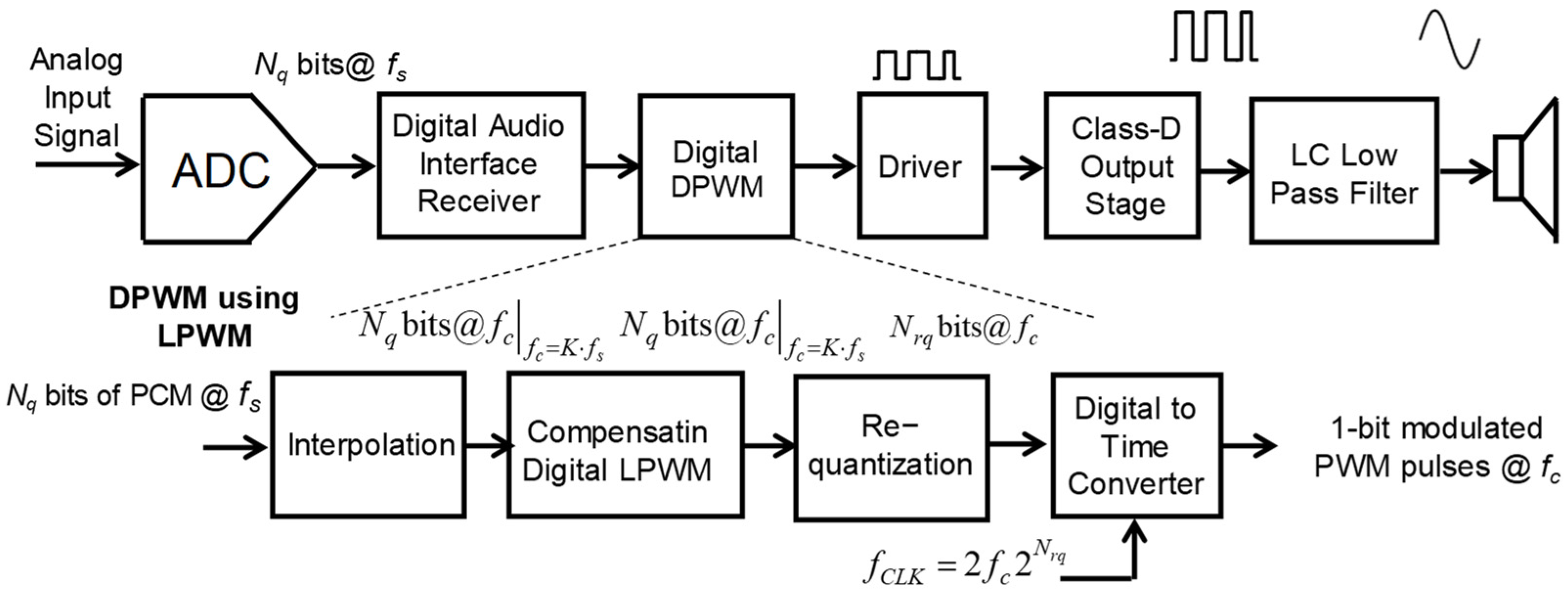
Figure 1 shows the general block diagram of an open-loop digital Class-D amplifier with LPWM digital modulation and pre-compensation, making it possible to emulate all four basic NPWM modulation methods [
7].
The input audio signal is converted into an
Nq-bit PCM data stream, which the digital modulator converts directly into a train of 1 bit physical DPWM pulses. In the interpolation process, additional signal samples uniformly distributed over the switching period
Tc are added into the PCM data stream at the ADC output. The modulating signal in this interval is approximated by rectilinear segments passing through the interpolated PCM samples. The digital values of the pulse-edge locations, the
tp (
n) rising edge and the
tk (
n) falling edge of the LPWM pulse within
n-th period
Tc of the switching frequency, calculated with a high
Nq = 32 bit resolution, are then requantized to a lower
Nrq-bit resolution (
Nrq < Nq), to moderate an excessive requirement of high clock frequency [
7]. At the calculated pulse-edge locations requantized to a 9 bit resolution, it is possible to implement a digital-to-time converter (DTC) on the basis of the hybrid method, to convert the calculated data into the physical train of the LBDD PWM pulses.
The requantized data are split into two parts consisting of 6 MSB (8:3) and 3 LSB (2:0) data bits; then, each
n-th period of the switching frequency is sequentially rewritten into LADD registers. The 6 MSB data are converted on the basis of the counter method using an STM32 microcontroller with its peripherals, while the remaining 3 LSB data are converted using a method based on the integrated 3 bit FAST TTL PTLDL [
17].
The timing of the signal processing blocks in
Figure 1 is based on the oscillator frequency of the three microcontroller AHB buses [
18].
The external converter based on the 3 LSB (2:0) PTD is controlled by the frequency.
The conversion frequency
fCONV of the ADC [
18] and the switching frequency are the same.
The delay time
td1 of one 3 bit PTDL segment, consisting of eight identical delay segments, results from the division of the clock period
TCLKh into eight parts.
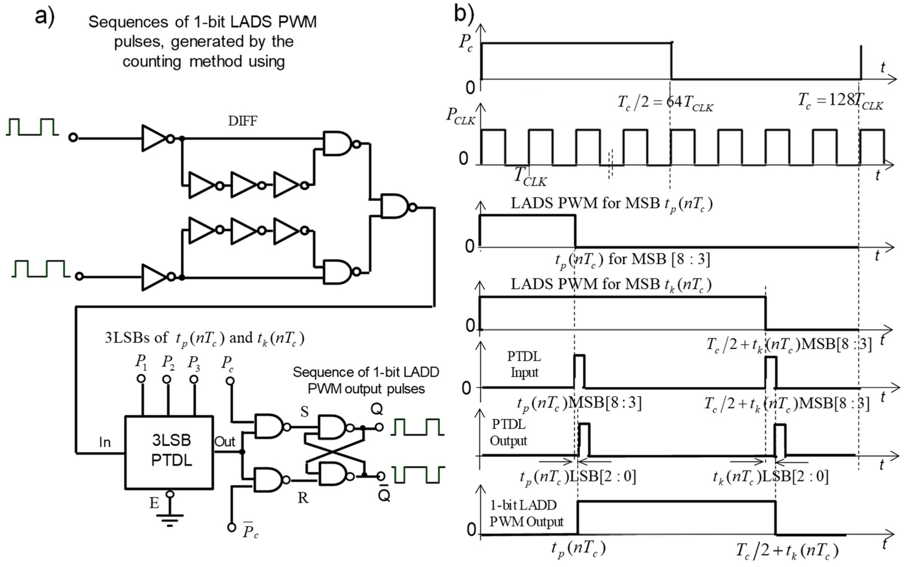
The conversion of the calculated and requantized 3 LSB LADD PWM audio data into a sequence of 1 bit LADD PWM pulses is shown in
Figure 2. Using 6 MSB (8:3) bits of the requantized values of the rising edge
tp (
n) and the falling edge
tk (
n) locations, which are stored in LADDL registers, the STM32 microcontroller and its advanced-control timers generate in each
Tc period two synchronous sequences of the linearized Class-AD single sided PWM (LADS PWM) signal. The falling edges of both generated LADS PWM signals are differentiated and then passed through a 3 bit PTDL. As a result, at the output of PTDL we get the spike pulses, which are delayed by the time programmed twice in each switching period
nTc for the 3 LSB (2:0) bits of the requantized values of the rising edge
tp (
n) and the falling edge
tk (
n) locations.
The delated spike pulses corresponding to the rising edge tp (n) locations, which occur at the PTDL output in the first half of the switching cycle Tc, set the RS output flip-flop, while the pulses that occur in the second half of the switching cycle Tc, which correspond to the falling edge tk (n) locations, reset this flip-flop. As a result, at the output of the flip-flop, the final 9 bit LADD PWM signal is generated.
Figure 3 shows the HBS implemented on the IRF9389PbF power MOSFET pairs, which are driven by the EL7158 high-performance inverting drivers. The left branch of the H-bridge is controlled by the
LADDLPWM signal generated for the direct audio signal, while the right branch of the H-bridge is controlled by the
LADDRPWM signal generated in the same way for the inverted audio signal. Shoot-through currents can be reduced by adding dead times in front of the edges of the control signals switching on the power transistors, thus also reducing EMI [
7]. These times are independently set on the rising edges of the signals driving of NMOSFETs (the
RGN resistors) and on the falling edges of the signals driving PMOSFETs (the
RGP resistors). Because the gate drivers and the HBS implemented on complementary MOSFETs are powered by the same voltage, a level shifter of the gate driver output signal is needed to ensure the proper
VGS voltage turning on the MOSFET, as well as to not exceed the maximum drain-to-source and gate-to-source breakdown voltages.
The independent setting of voltage levels in the low VL and high VH states at the output of the EL7158 driver allows for the optimal selection of the control voltage amplitude. The EL7158 controller also has very good dynamic characteristics, the same rise and fall times, and the same delay times of switching on and off the output signal; thus, it does not introduce additional distortions of the DPWM signal at the HBS output.
At the output of the HBS, a second-order low-pass LRC filter is typically used to suppress the high-frequency components of the LBDD PWM signal and to pass the audio components to the load. The magnetic components of the output filter, which should be put as close as possible to the HBS output, increase the complexity, size, and cost of the amplifier.
3. Filterless, Open-Loop Digital Class-BD Amplifiers with Constant Voltage at the CM Output
Figure 4a shows an open-loop low power Class-BD amplifier with constant voltage at the CM output implemented on four ultrahigh-current EL7158 pin drivers. The EL7158 high-performance inverting drivers are controlled by the extended digital modulator based on the LBDD PWM modulation scheme (
Figure 4b) and have appropriately set voltage levels on the VL and VH pins to obtain the necessary voltage levels at the driver outputs, depending on the status of the IN pins. The extended LBDD PWM modulator is based on the hybrid 9 bit LBDD modulator, described in
Section 2, with an additional logic that generates all control signals
S1,
S2, and
S3. The outputs of drivers 1, 2 and drivers 3, 4 are connected in parallel; however, when drivers 1, 3 are active with OE in the high state, then drivers 3, 4 with OE in the low state have the outputs placed in the three-state mode (floating). On the contrary, when drivers 3, 4 are active, the outputs of drivers 1, 2 are placed in the three-state mode.
In order to not exceed the continuous output current of the driver (0.5 A), with a supply voltage of
VDD = 18 V, the load resistance
RL must not be lower than 40 Ω. At the differential mode (DM) output and the balanced CM output of the amplifier, we receive near-perfect voltage waveforms, even at high switching frequency, as presented in
Figure 4c.
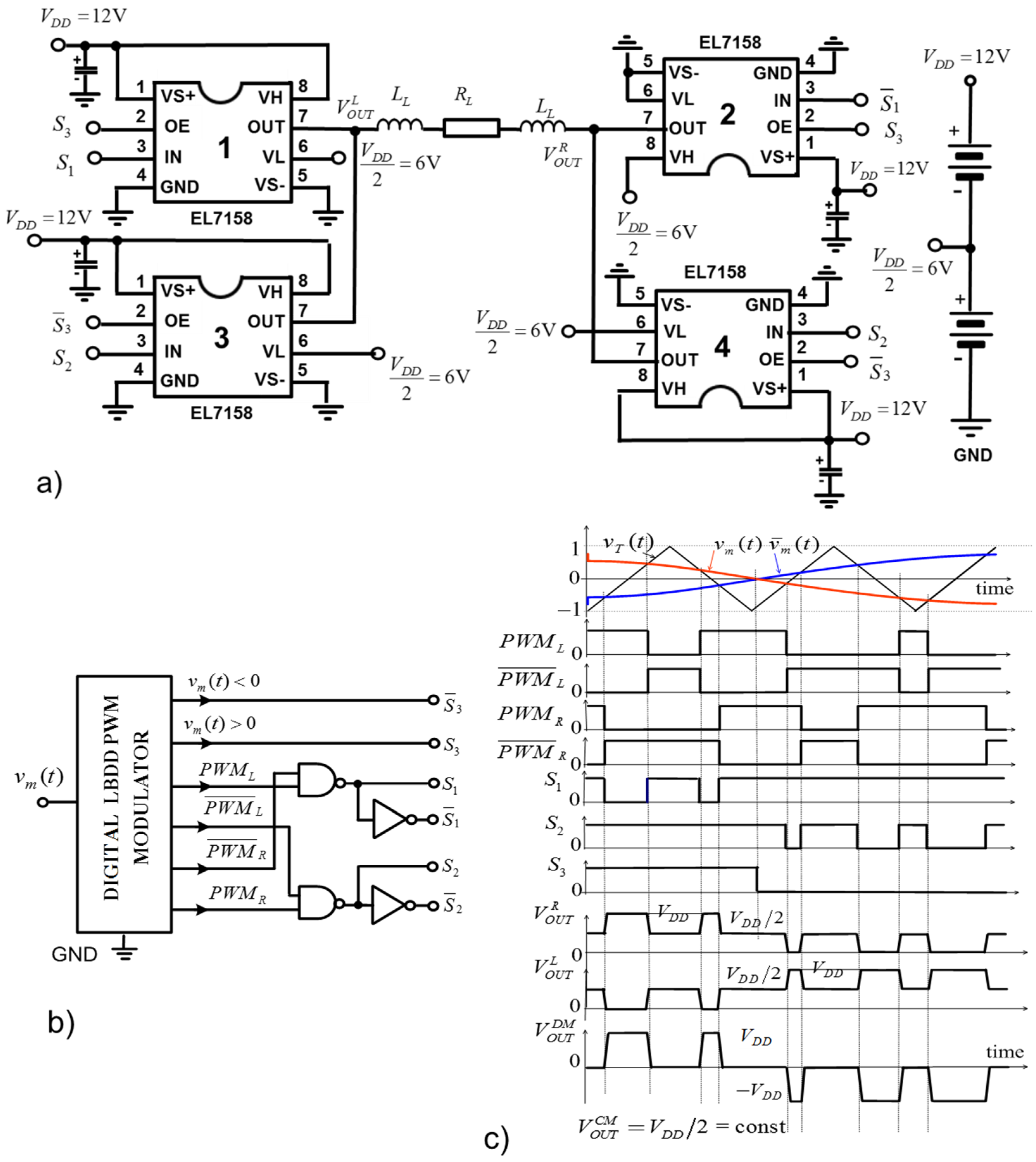
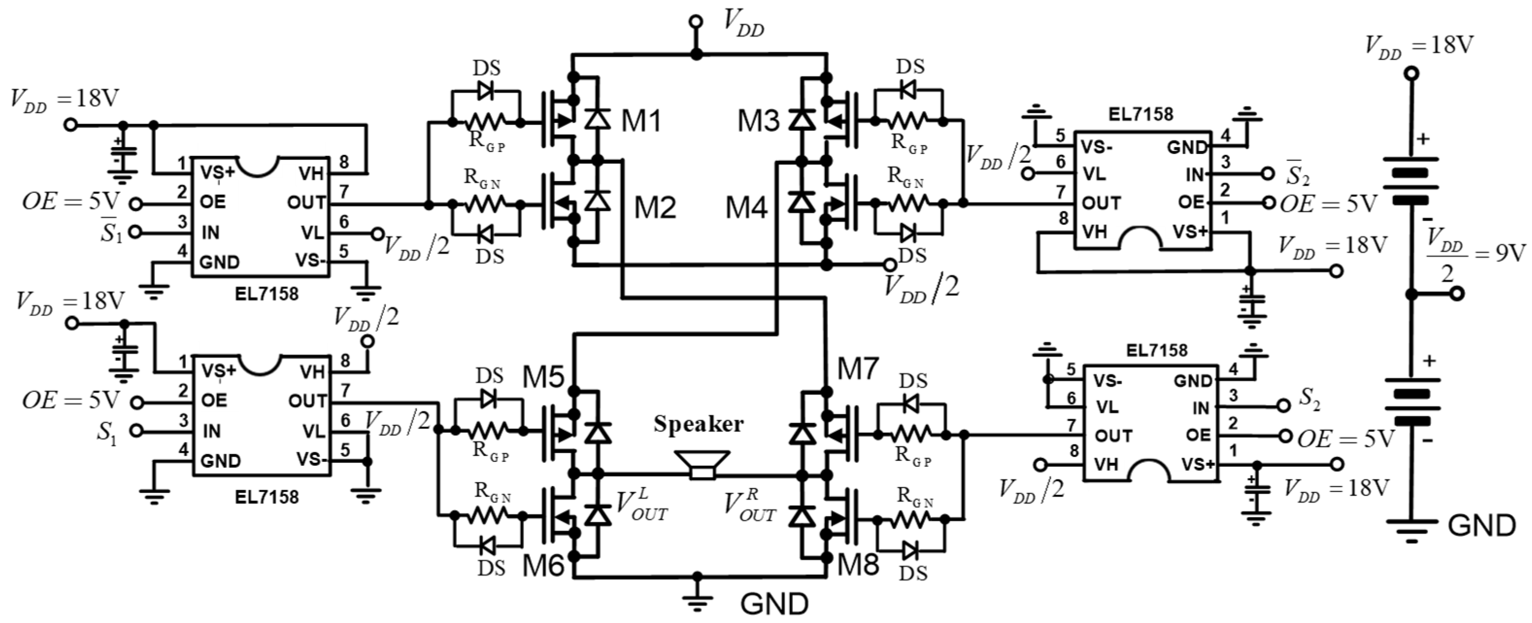
The architecture of the second proposed amplifier, shown in
Figure 5, consists of two typical, but differently powered, Class-BD amplifiers built on the IRF9389PbF complementary power MOSFET pairs. The upper H-bridge on the (M1–M4) MOSFETs is powered from the upper
VDD/2 power supply, while the lower H-bridge on the (M5–M8) MOSFETs is powered from the lower
VDD/2 power supply. The resultant output signals on the left
and right
sides of the amplifier are the result of a series summation of the output voltages of the upper and lower H-bridges, respectively, as shown in
Figure 5.
Both H-bridges are driven by the EL7158 high-performance inverting drivers controlled by the extended digital modulator based on the LBDD PWM modulation, as presented in
Figure 4b, and they have appropriately set voltage levels on the VL and VH pins to obtain the necessary voltage levels at the driver outputs, depending on the status of the IN pins. The switching frequency of the output stage MOSFETs is twice as high as the switching frequency in a conventional Class-BD amplifier (in
Figure 3), since the control signals
S1 and
S2 are generated by an extended LBDD PWM modulator of this frequency. This results in higher switching power losses. In this circuit, the
S3 signals are not used, and all EL7158 drivers are active, with their OE inputs
OE = 5 V. Moreover, in this system, the set delay times before the edges of the control signals switching on the power transistors prevent the shoot-through currents and also reduce EMI. These times are independently set on the rising edges of the signals driving NMOSFETs (the
RGN resistors) and on the falling edges of the signals driving PMOSFETs (the
RGP resistors). The amplifier is loaded with resistance
RL = 4 Ω or
RL = 8 Ω. At the differential mode (DM) output and the balanced CM output of the amplifier, we receive near-perfect voltage waveforms, even at high switching frequency, as presented in
Figure 4c.
4. Simulation and Measurement Results
SPICE simulations and experimental results were used to compare the parameters of the proposed digital Class-BD amplifier with constant voltage at the CM output (
Figure 5) with the parameters of the conventional digital Class-BD amplifier using LBDD PWM modulator (
Figure 3). Both amplifiers were implemented on complementary IRF9389PbFF MOSFET pairs, driven by inverting high-performance EL7158 drivers and powered by the same voltage:
VDD = 18 V. They were tested for two switching frequencies:
fc1 = 328 kHz or
fc2 = 164 kHz, using for each of them two different load impedances:
RL = 4 Ω,
L = 15 µH or
RL = 8 Ω,
L = 30 µH.
A low-power Class-BD audio amplifier with balanced CM output, implemented on four ultrahigh-current EL7158 pin drivers, was tested for VDD = 12 V and two different load impedances: RL = 40 Ω, L = 150 µH or RL = 80 Ω, L = 300 µH.
First, time domain waveforms and frequency spectrum characteristics of DPWM signals were simulated using Matlab
® tools. The frequency spectrum was estimated by storing a number of pulses of the LBDD DPWM output signal, which represents more than one period of the modulating waveform.
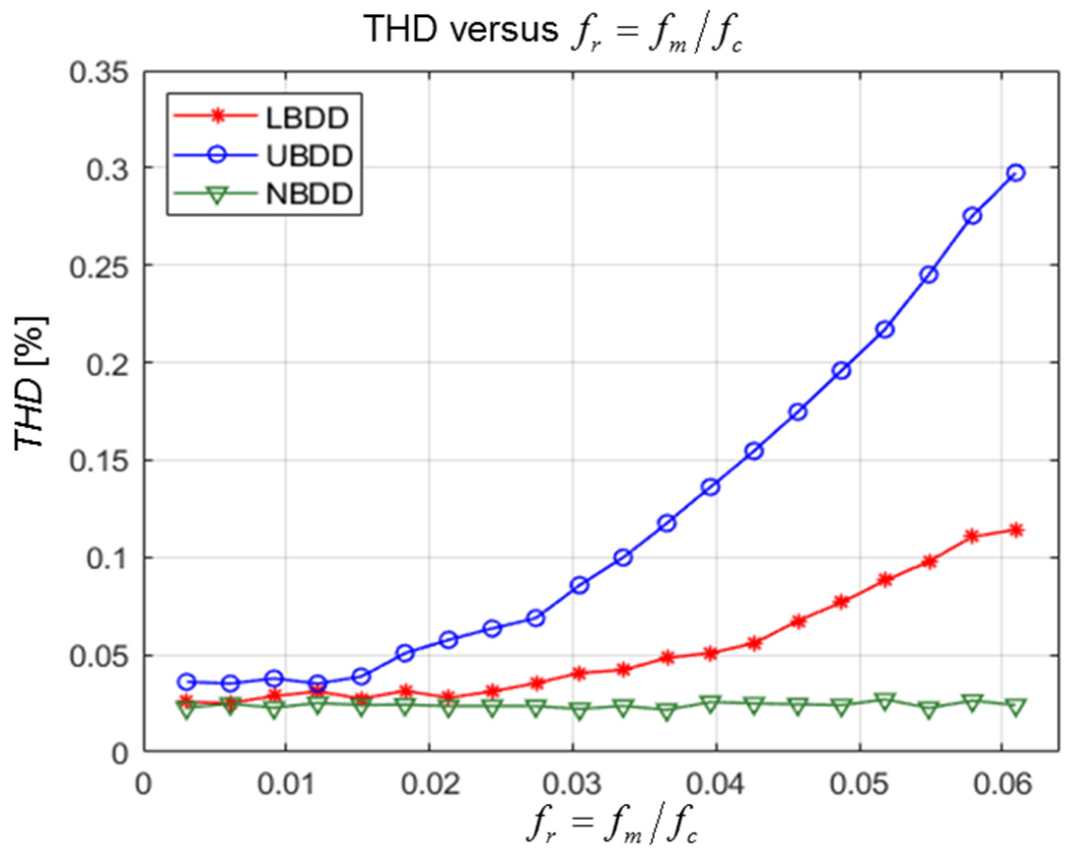
Figure 6 shows a comparison of the THD coefficients for three modulation methods, LBDD, NBDD, and UBDD, versus relative frequency
fr = fm/fc. This comparison shows that, even for a simple LBDD algorithm for
Q = 1 between two adjacent samples
y0 (
n) and
y2 (
n) of the audio signal, only one intermediate sample
y1 (
n) is generated with the distance:
TQ = Tc/2, and using a recursive noise shaping model with two feedback loops allows a significant improvement in the modulator’s linearity.
In each H-bridge branch of the amplifier output stage, it is necessary to insert a blanking period between either high-side turn-off and low-side turn-on or low-side turn-off and high-side turn-on when switching transistors to reduce shoot-through or a rush of current through both MOSFETs. The use of R
G gate resistors with antiparallel Schottky diodes, as in
Figure 3 and
Figure 5, allows adjustment of the MOSFET turn-on delay time (
RGN allows adjusting the delay time of the rising edges of the PWM signal, while
RGP allows adjusting the delay time of the falling edges) independently. During turn-off, the antiparallel Schottky diode shunts out serial resistor
RG, providing a significant reduction in turn-off delay time.
For optimal values of the gate resistors
RGN and
RGP, we receive turn-on delay times
tdN for NMOS and
tdP for PMOS, for which a compromise is possible to obtain an acceptable level of THD and a significant limitation of the shoot-through currents. In order to determine the values of these resistances, the currents of the drains and bypass diodes of transistor pairs M1, M2 and M3, M4 in the output stage in
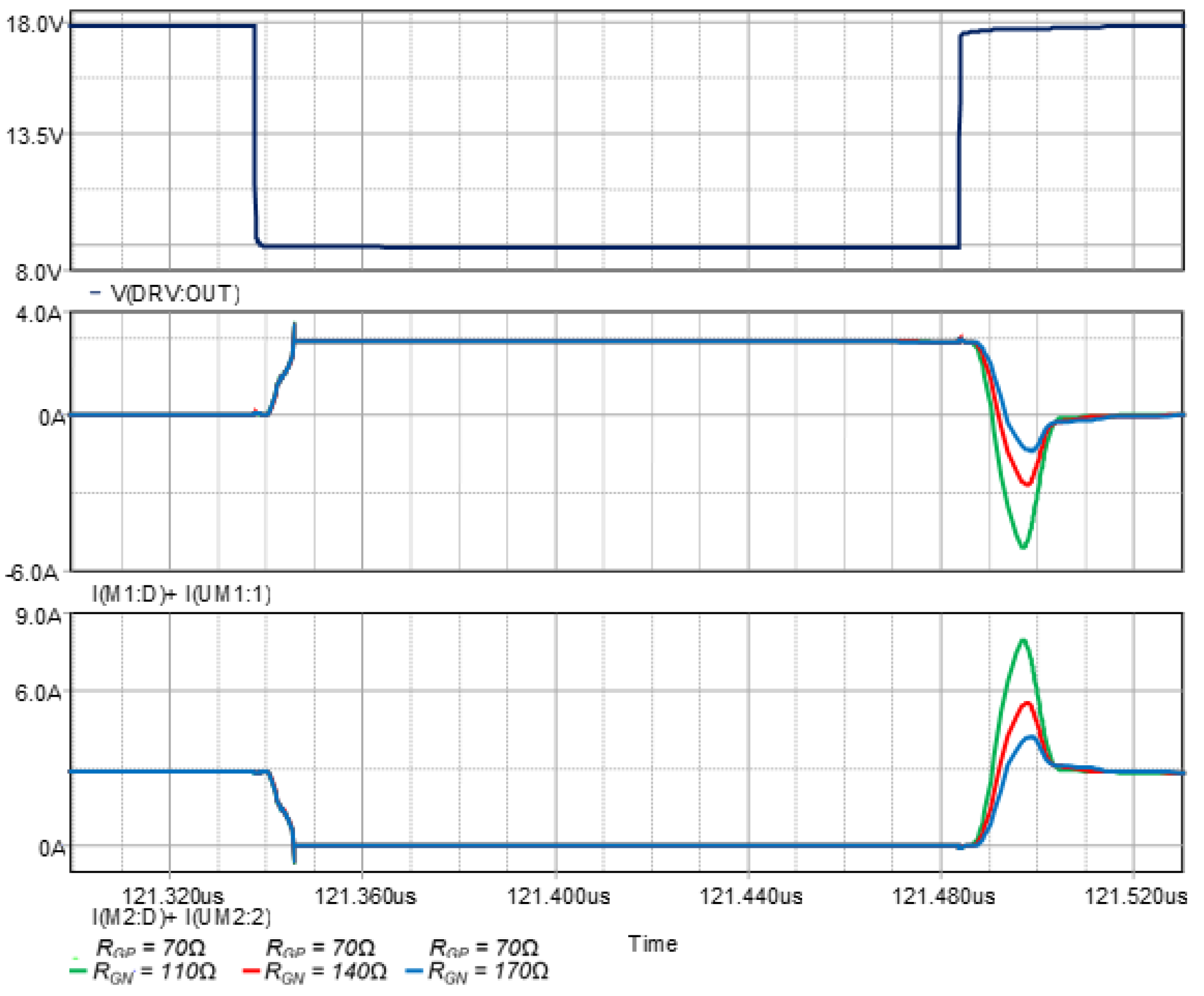
Figure 3a were simulated in PSPICE, using the transient analysis with the “Parametric Sweep” option.
Figure 7 shows the currents of drains and diodes shunting M1 and M2 transistors in one period of the DPWM signal, when switching a constant load current, and when one of the transistors is inversely conducting. The optimal resistances
RGN = 110 Ω,
RGP = 70 Ω, were selected on the basis of the transient, multirun parametric analyses at the specifying sweep parameters of the gate resistors:
RGN [110, 140, 170] Ω and
RGP [40, 70, 110] Ω. For the optimal resistances, the shortest turn-on delay times,
tdN for NMOS and
tdP for PMOS, as well the greatest limitation of the shoot-through current amplitudes, were obtained.
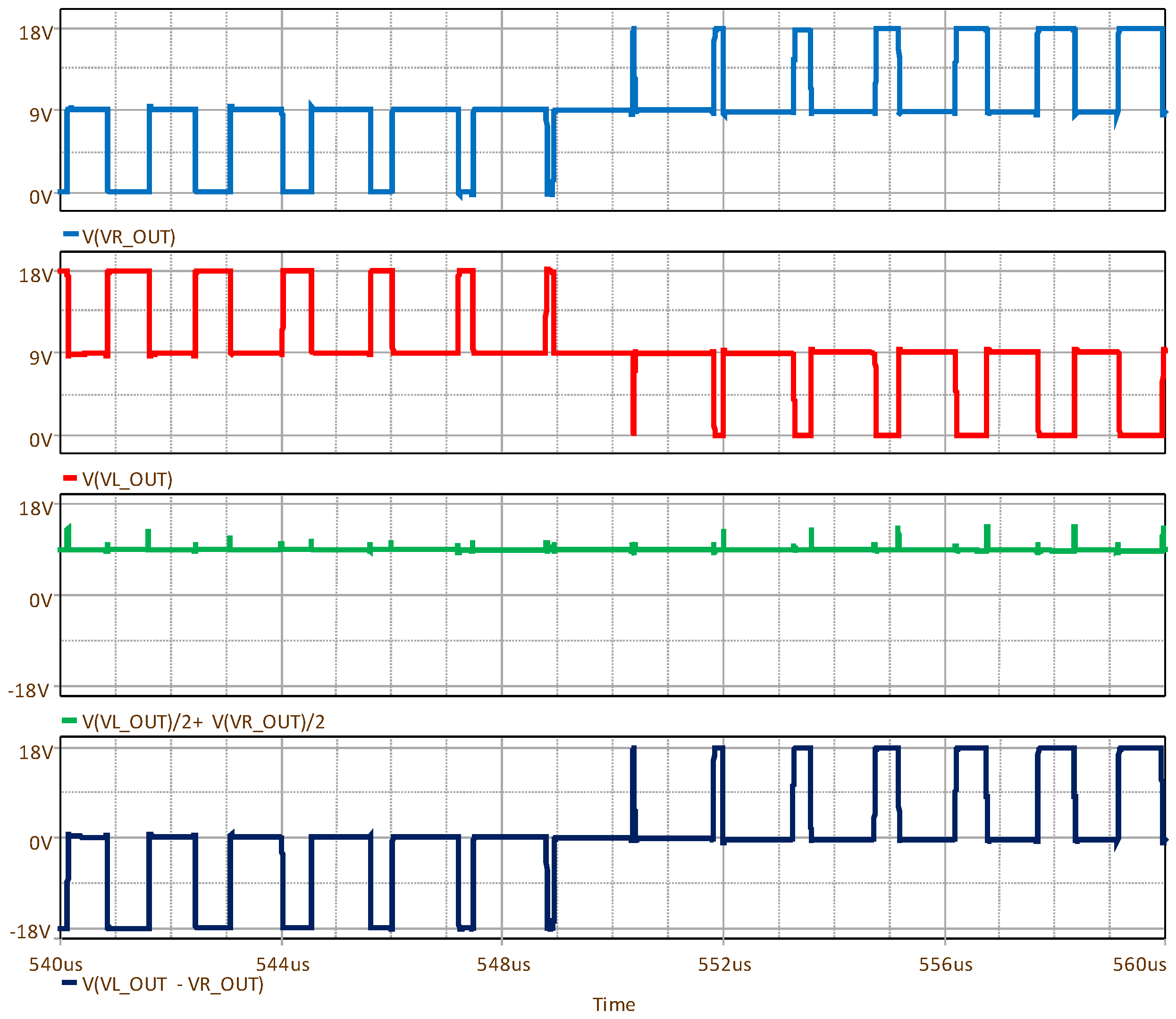
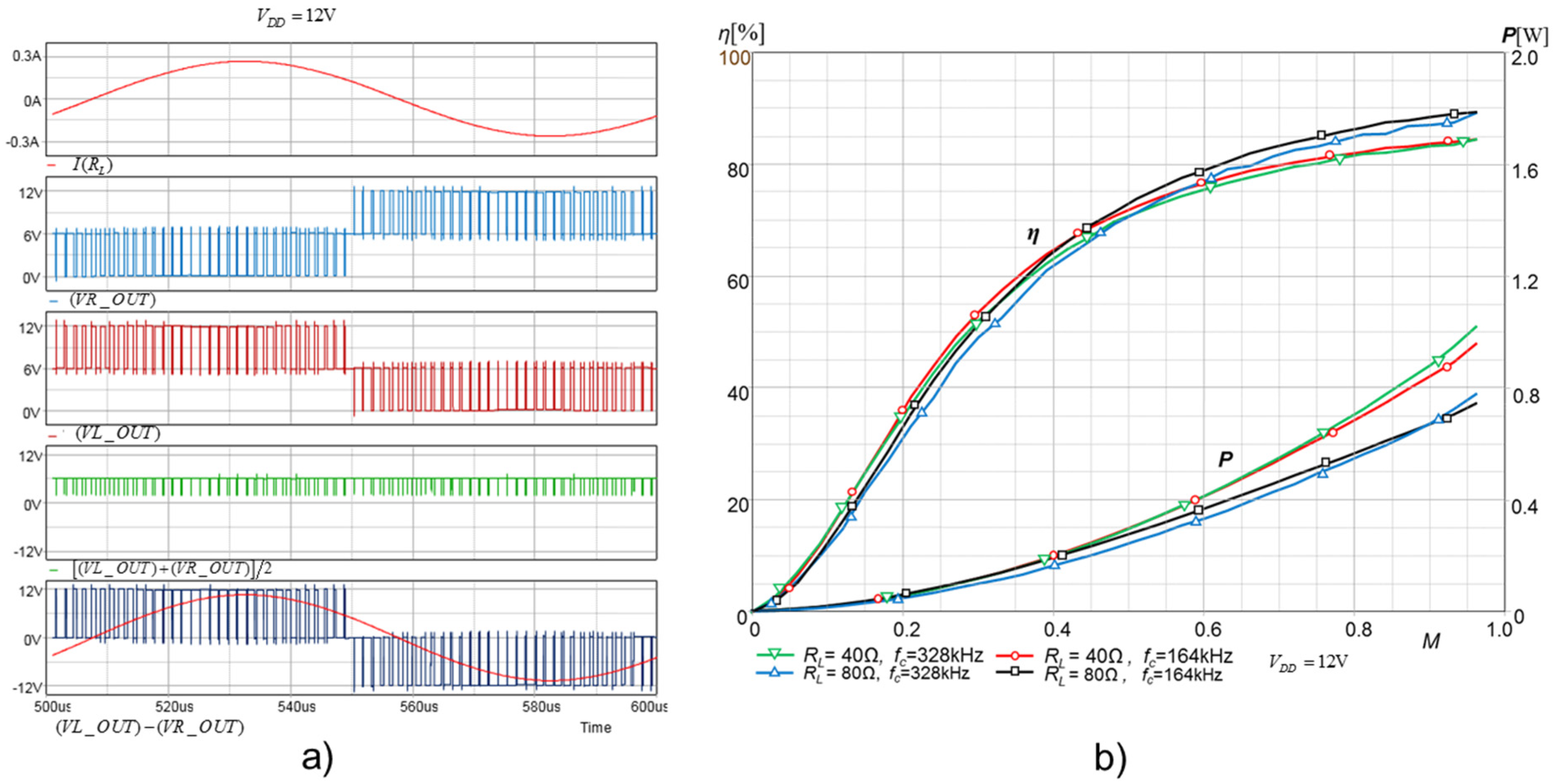
Figure 8 shows the SPICE-simulated time waveforms of the load current and output voltages in DM and CM modes of the Class-BD amplifier with balanced CM output (from
Figure 5), at
RL = 4 Ω,
L = 15 µH, and
fc = 328 kHz, as well as part of the period of the modulating signal with frequency
fm = 10 kHz.
The circuit has a perfectly balanced CM output with a constant voltage VDD/2, although very small spikes are generated at this output when switching transistors. The switching frequency of the output stage MOSFETs is twice as high (2fc) as the switching frequency fc of the conventional Class-BD amplifier, which may result in higher switching power losses.
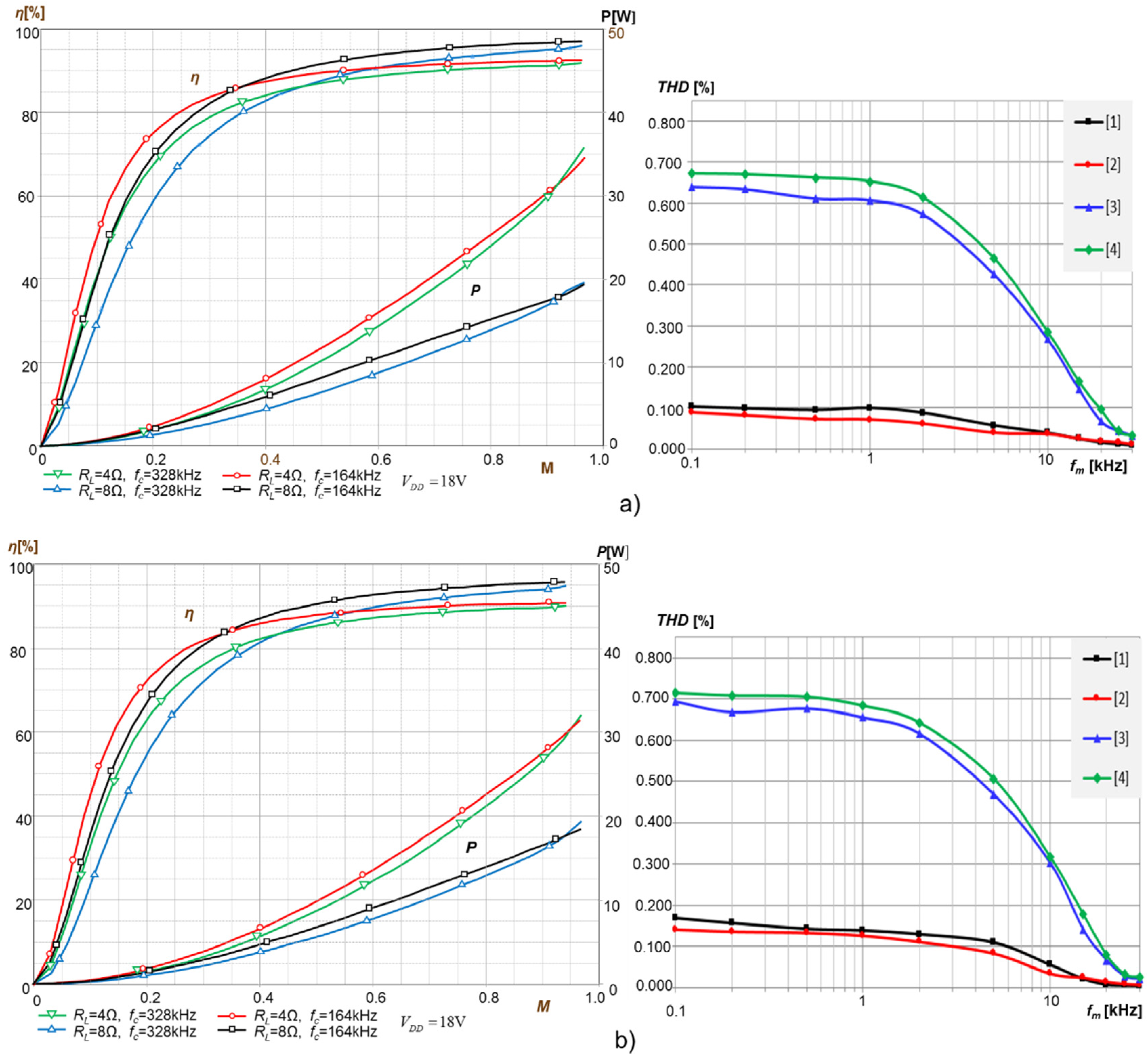
Figure 9 shows the output power and efficiency versus modulation index
M, as well as THD versus the frequency of the modulating signal, of the new digital Class-BD amplifier with a balanced CM output (in
Figure 5) using the extended LBDD PWM modulator compared to the conventional Class-BD amplifier (
Figure 3) using an LBDD PWM modulator. The characteristics were determined for two switching frequencies,
fc1 = 328 kHz or
fc2 = 164 kHz, using for each of them two different load impedances:
RL = 4 Ω,
L = 15 µH or
RL = 8 Ω,
L = 30 µH.
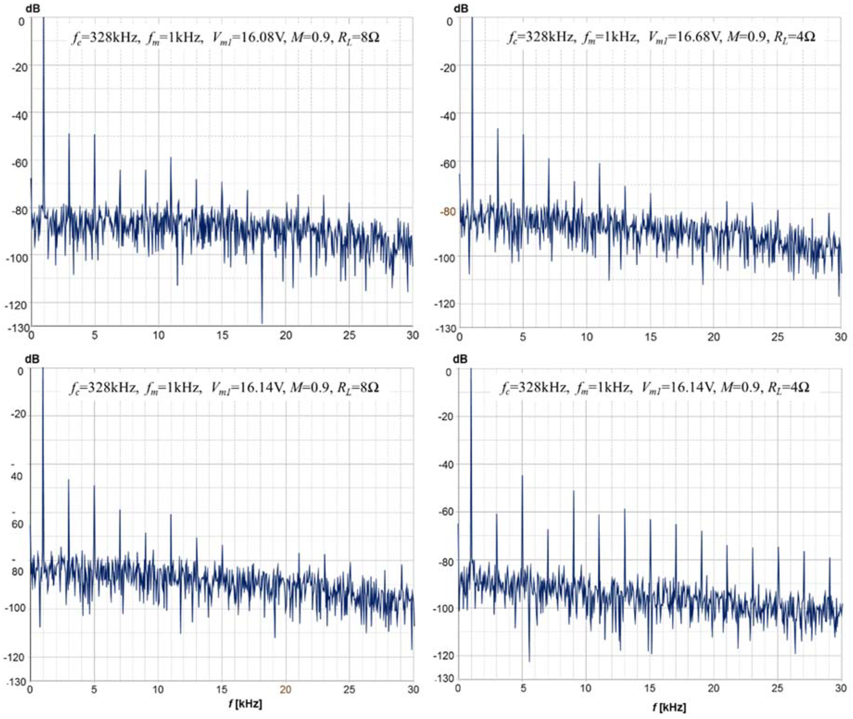
The THD characteristics versus the
fm frequency of the modulating signal were determined on the basis of the THD + N frequency spectra of the output voltage on the load resistance, in the band up to 30 kHz, examples of which are shown in
Figure 10.
The Class-BD amplifier with constant voltage at the CM output has almost the same the output power and efficiency characteristics as the conventional one, but it exhibits a slightly higher level of nonlinear distortions, which are caused by the distorted DPWM waveform being generated in the output stage by nonideal MOSFET switches. The most significant contribution to the total THD is represented by switching timing errors added by the gate drivers, such as dead-time, ton/toff, and tr/tf. The distortions are also caused by nonlinearity in the DPWM signal from the modulator to switching stage due to limited resolution, as well as jitter in timing. Another source of distortions is represented by unwanted characteristics in the switching devices, such as finite ON resistance (particularly when the conductive branch of the output stage contains four MOSFET switches), finite switching speed, or body diode characteristics.
Figure 11a shows the-simulated time waveforms of the load current and output voltages in DM and CM modes of the low-power Class-BD amplifier with balanced CM output and implemented on four EL7158 drivers (
Figure 4a), with
RL = 40 Ω,
L = 150 µH,
fc = 328 kHz, and
fm = 10 kHz, while
Figure 11b shows the characteristics of the output power and efficiency versus modulation index
M, for two switching frequencies,
fc1 = 328 kHz or
fc2 = 164 kHz, using for each of them two different load impedances:
RL = 40 Ω,
L = 150 µH or
RL = 80 Ω,
L = 150 µH. This amplifier has lower efficiency (approximately 85%), mainly due to the conduction power losses, because the conductive branch of the output stage contains four MOSFET switches (each of them with a resistance of 0.5 Ω) connecting the output pin OUT of the driver to the input pins VH or VL, depending on the status of the IN pin. The conventional Class-BD amplifier using LBDD PWM modulator contains two MOSFET switches in the conductive branch of the output stage, which are switched at the switching frequency
fc, while the conductive branch of the output stage of Class-BD amplifier with balanced CM output, using an extended LBDD PWM modulator, contains four MOSFET switches, which are switched at the frequency of 2
fc. The practical implementation of this amplifier is very easy, while providing a perfectly balanced CM output with a constant voltage
VDD/2.
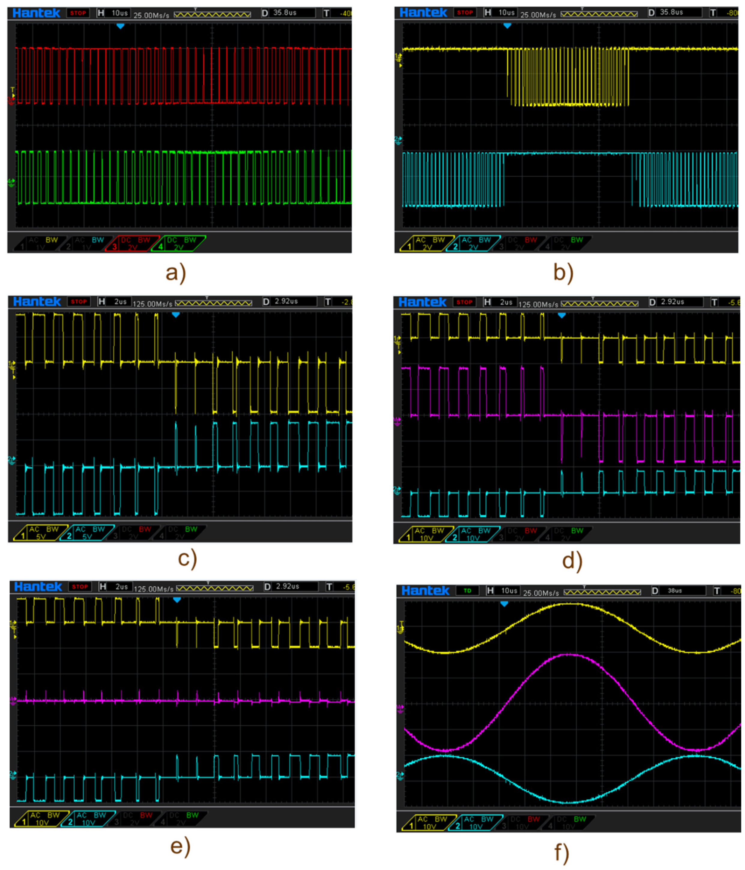
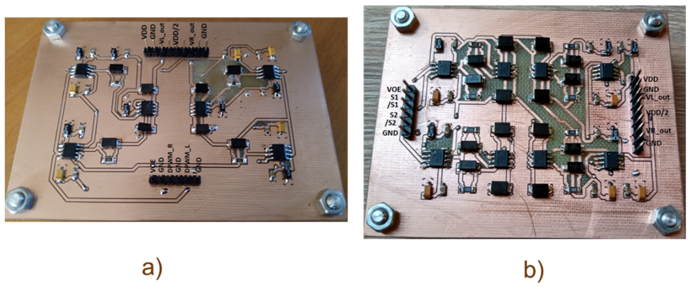
Figure 12 shows a photograph of two PCBs containing the output stages of two tested Class-BD amplifiers: (a) conventional Class-BD amplifier (in
Figure 3); (b) Class-BD amplifier implemented on complementary MOSFET pairs (in
Figure 5). All gate drivers of the output stages are steered by signals generated by the digital extended LBDD PWM modulator.
Load impedances are connected to the PCBs with short cables from the outside.
The following equipment was used to test the amplifiers:
- −
Rigol DG1032Z function generator;
- −
Hp 8593 Agilent spectrum analyzer, 1 kHz–2.9 GHz;
- −
DSO4254B advanced digital oscilloscope 4 × 250 MHz.
Figure 13 shows the oscillograms of the control signals generated by the hybrid 9 bit LBDD PWM modulator in
Figure 4b with extended architecture and oscillograms of the output voltages in DM and CM modes of the Class-BD amplifier with constant voltage at the CM output (in
Figure 5).
5. Discussion
We described and tested two new and original open-loop digital Class-BD audio amplifiers with constant CM output voltage. The output stage of the first, low-power Class-BD amplifier was implemented using only four ultrahigh-current EL7158 pin drivers, while the second, higher-power Class-BD amplifier was implemented using four complementary HEXFET IRF9389PbF power MOSFET pairs, formed into two cooperating and interacting typical H-bridges and driven by four ultrahigh-current EL7158 pin drivers. The drivers have appropriately set voltage levels on the VL and VH pins and are controlled by an extended LBDDPWM modulator based on a digital, hybrid 9 bit LBDD PWM modulator, described in detail in a previous study [
7].
Extensive experimental and SPICE simulation studies were conducted to compare the performance of the proposed Class-BD amplifier with balanced CM output to the performance of the conventional Class-BD amplifier. As presented in
Figure 9, the characteristics of the output power and the efficiency versus modulation index M, as well as THD versus the audio signal frequency, were tested for two switching frequencies,
and
, using with each switching frequency two different load resistances:
RL = 4 Ω and
RL = 8 Ω. As we can see in
Figure 9, the proposed Class-BD amplifier with a balanced CM output has a slightly better performance at the DM output than the conventional one.
For example, for RL = 4 Ω and , when adjusting the modulation index M from 0 to 0.96, the load power PL at its differential output changes in the range from 0 to 35 W and is higher than the load power PL of a conventional Class-BD amplifier in this range from 0 up to 2.5 W, while the efficiency ƞ varies from 0% to 96% and is higher in this range from 0% to 1% than the efficiency of a conventional Class-BD amplifier. For other combinations of RL and fc, the load power PL and the efficiency ƞ of the Class-BD amplifier with balanced CM output are also slightly higher than for the conventional Class-BD amplifier, but with a narrower range than the example above.
In order to verify the results of the simulation tests, actual measurements of parameters were made at selected points of the simulated characteristics in
Figure 9 on the model of the implemented amplifier in
Figure 5 (PCB in
Figure 11b). The efficiency
ƞ was determined on the basis of the measurement of the load power
PL in the resistance
RL and the
PDC power of the source powering the output stage of the amplifier, while the spectrum analyzer was used to measure the harmonic content of the output signal spectrum in the band from 30 Hz to 30 kHz. For example, for
RL = 4 Ω and
, when adjusting the modulation index M from 0 to 0.96, the load power
PL changes in the range from 0 to 30 W and is lower than the simulated load power
PL in this range from 0 up to 1.5 W, while the efficiency
ƞ varies from 0% to 90.3% and is lower in this range from 0% to 1% than the simulated efficiency. For other combinations of
RL and
fc, the measured load power
PL and the efficiency
ƞ are also slightly lower than simulated values but with a narrower range than the example above. The obtained measurement results are slightly worse than the simulation results, because the simulations did not take into account the resistances of the wires and paths to the power supply and the resistance of the real coil in the load.
As we can see in
Figure 4c and the oscillograms in
Figure 13b, at the DM output and the balanced CM output of the amplifier, we receive near-perfect voltage waveforms. The upper parts of the output voltage
and
waveforms on the left and right branches of the output H-bridge are generated by the upper HBS on the (M1–M4) MOSFETs, while the lower parts are generated by the lower HBS on the (M5–M8) MOSFETs. Each of the three states at the DM output of the amplifier is the result of switching on only one MOSFET pair, causing low conduction power losses. Moreover, switching of each complementary pair of transistors in the upper or lower H bridge occurs at half the supply voltage
VDD/2, which results in lower switching power losses than in the conventional Class-BD amplifier.
As presented in
Figure 7, the THD characteristics as a function of the
fm input signal frequency were determined on the basis of the THD + N frequency spectra of the output voltage on the load resistance, in the band up to 30 kHz. All tested amplifiers show some distortion at the DM outputs, with the largest for
fc1 = 328 kHz,
RL = 4 Ω: conventional Class-BD amplifier up to 0.7%, and Class-BD amplifier with constant voltage at the CM output up to 0.68%. Much lower distortions, below 0.1%, are obtained for both amplifiers at
fc2 = 164 kHz (power MOSFET transistors, controlled by
S1,
S2 signals, are switched with the frequency of 2
fc = 328 kHz). These distortions are a result of the distorted LBDD PWM time waveforms generated by the output stages of these amplifiers, caused by the switching timing errors. It is well known that switching timing errors in the gate signals, due to turn-on delay times of the transistors, in particular, have the most significant contribution to nonlinearity in DM output stages.
Comparing the obtained results with the results of other studies, it can be concluded that the measured and simulated performance of the proposed amplifier is slightly better than that of similar Class-BD amplifiers with balanced CM output, described, e.g., in [
10,
11,
12].
As presented in [
10], a Class-BD amplifier with the power of 20 W/channel with almost zero CM radiation emission had the configuration of the H6-type output stage and used the PSCPWM modulation method. The H6-bridge contained two additional series switches M5 and M6 connected parallel with the load, which were used to shunt the bidirectional inductive load current when M1–M4 were off and to set both outputs at
VDD/2 with the help of shunt resistors
Rb connected parallel with M1–M4 transistors. With switching frequency of 250 kHz, power supply of 12 V, and
RL = 4 Ω, the amplifier could deliver 10 W at the efficiency
ƞ up to 89% and THD + N up to 0.6%, whereas, with supply of 24 V, it could deliver 18 W at the efficiency
ƞ up to 81% and THD + N up to 0.6%. The significant reduction in efficiency was due to the additional power losses in shunt resistors
Rb connected in parallel with M1–M4 to set both outputs at
VDD/2, which also increased the rise and fall times of the PWM output pulses, contributing to a further increase in switching power losses.
The output stage of the open-loop Class-BD audio amplifiers presented in [
11,
12] with balanced CM included a typical H-bridge with four MOSFETs and four additional MOSFET switches that balanced and maintained the CM output. These amplifiers employed the extended NBDD PWM or PSC PWM modulation scheme. With a switching frequency of 328 kHz, power supply of 24 V, and
RL = 4 Ω, the amplifier could deliver 56 W at the efficiency
ƞ up to 91% and THD + N up to 0.76%, whereas, with
RL = 8 Ω, it could deliver 32 W at the efficiency
ƞ up to 96% and THD + N up to 0.73%.
The performance of the compared amplifiers is similar, but the control system for the proposed Class-BD amplifier in this paper is simpler and easier to implement.
6. Conclusions
New and original architectures and implementations of two filterless, open-loop digital Class-BD audio amplifiers with constant common mode (CM) output voltage were presented.
The extended digital LBDD PWM modulator uses a linearized Class-BD double-sided modulation scheme with pre-compensation, enabling the most faithful emulation of the natural NBDD PWM and, thus, providing an attractive spectral characteristic at the DM output, similar to the NBDD PWM, while simultaneously providing a balanced CM output with constant voltage at this output. The simple filtering of the DPWM signal at the DM output by the resistive–inductive impedance of the loudspeaker and the elimination of CM signal filtering at the CM output (constant voltage at this output) are the most desirable features of a filterless Class-D amplifier without an external LC filter. The elimination of CM signals also significantly contributes to the reduction in EMI, particularly those produced on the cables connecting the loudspeaker to the HBS terminal.
Proposed amplifiers with very original topologies, due to their simple design and easy control (no galvanic isolation of control signals and no floating bias power supplies), which generate no CM voltage and feature excellent DM performance, similar to conventional Class-BD amplifiers, are very attractive solutions for filterless Class-BD amplifiers.
The topology of the amplifier output stage is formed by two typical H bridges in which MOSFET switching processes are the same as in a conventional Class-BD amplifier; therefore, it is easier and more effective to reduce the amplitudes of the shoot-through currents. Switching of each complementary pair of transistors in the upper or lower H bridge occurs at half the supply voltage VDD/2, which results in lower switching power losses than in a conventional Class-BD amplifier.
It seems that the proposed new Class-BD amplifier topology is easier to implement and more efficient than the H5, H6, and HERIC topologies that are used in transformerless full-bridge PV grid-tied inverters [
19,
20].


