Article

DC-Link Capacitor Voltage Balancing Control of a Five-Level Regenerative AC Electronic Load Using One-Cycle Control †

Department of Electrical Engineering, Hanyang University, Seoul 04763, Korea
This paper is an extended version of a paper published in Proceedings of the 2011 Twenty-Sixth Annual IEEE Applied Power Electronics Conference and Exposition (APEC), Fort Worth, TX, USA, 6–11 March 2011.
Energies 2021, 14(19), 6101; https://doi.org/10.3390/en14196101
Submission received: 28 July 2021 / Revised: 8 September 2021 / Accepted: 21 September 2021 / Published: 24 September 2021
(This article belongs to the Section F: Electrical Engineering)

Abstract

:
High voltage electric power equipment requires rigorous regulation testing to specific standards which ensure proper and safe operation in the grid. Manufacturers conduct these tests in order to prove standard compliance and product liability. Variable linear or nonlinear loads are necessary for testing medium voltage (MV) high power AC power converters. Generally, those AC power converters or power supplies require performance validation, burn-in and/or lifetime testing under different load conditions, defined by the end-user or standards for the given applications. For flexible and efficient MV verification testing, this paper presents a five-level multilevel converter-based MV regenerative AC electronic load with one-cycle control (OCC), which is based on five-level diode-clamped multilevel converters with back-to-back structure and can emulate any impedance load. In this paper, especially the dc-link capacitor voltage balance of the proposed multilevel MV regenerative AC load is deeply analyzed. Simulation and experimental results are presented to verify the dc-link voltage balance performance of the proposed multilevel MV regenerative AC electronic load.

Graphical Abstract

1. Introduction

For utility companies the reliability of their power transmission and distribution equipment installed in the power grid is vital. The manufacturers of the high voltage power equipment can prove that their products have been tested according to international standards—IEC 62271, 61869, 60044 and 60076 standards, meet end-user specifications and relevant safety regulations. For this purpose, various loads are required to validate the performance, to carry on burn-in and to conduct lifetime testing of power conversion equipment, including uninterruptible power supplies, AC motors, turbine generators, inverters and power system equipment. Traditionally, high power load banks provide a practical solution for the manufacturers of the high-power equipment, but they are typically large, bulky and energy-consuming. Many load banks use a combination of resistors, inductors, capacitors and/or diode rectifiers to emulate various load conditions. When a different load parameter is required, reconnection of the load bank is necessary, which can be labor-intensive and time-consuming. This situation has led to the commercialization of some electronic loads that feature manual dial-in or automatic load adjustment, suitable for convenient and fast product testing. However, these electronic loads are limited in terms of both voltage and power rating. At present, these types of electronic loads are only available at low voltage, 400 V and low power level, 20 kVA per phase [1].
For MV verification, the testing equipment is generally not regenerative and still burns 100% testing energy. Energy consumption for power equipment testing is a serious problem, especially for high power MV applications. To recycle the testing energy, high voltage multilevel power electronic converters with back-to-back structure play an essential role in high voltage and medium voltage (MV) power applications. For high power MV applications, three-level or five-level diode-clamped multilevel converters (DCMCs) have been widely adopted in high power back-to-back systems. To obtain sinusoidal waveforms and reduce harmonic components, five-level DCMC-based back-to-back configuration has been receiving more attention recently [2]. However, the primary obstacle of the five-level DCMC-based back-to-back structure is control complexity to control 48 switching devices for the three-phase and achieve charge balance of four dc-link capacitors, for example, by using a modified space vector pulse width modulation (SVPWM) and a capacitor current prediction algorithm with or without an auxiliary hardware circuit that increases the complexity and the cost of the power conversion multilevel converters. There are commonly two types of the PWM methods to balance the dc-link capacitor voltages of the five-level DCMCs with or without back-to-back structure: (1) modified carrier-based SPWM [2,3,4,5] and (2) modified SVPWM [6,7,8,9,10]. Generally, the carrier-based SPWM technique is much simpler than the SVPWM method. As far as the implementation of the SVPWM technique is concerned, it is computationally very difficult to realize.
In [2], a MV adjustable-speed motor drive system based on two five-level DCMCs with back-to-back structure was proposed with 3 kHz four level-shifted carrier signals and four buck-boost choppers for achieving voltage balancing between four dc-link capacitors. The additional buck-boost choppers increase the complexity, the size and the cost of the proposed MV motor drive system. An auxiliary capacitor-based dc-link balancing approach was presented in [3] to equalize the dc-link capacitor voltages of the five-level DCMC by utilizing the auxiliary capacitor as an equalizer between the capacitors of different voltages. The proposed balancing hardware circuit-based method can be applied to both the carrier-based SPWM and the SVPWM but requires additional circuits and control, which would increase hardware complexity and system failure. A new carrier-based SPWM method with voltage balancing capability was proposed for the five-level DCMCs with back-to-back structure in [4]. For the back-to-back configuration, the unbalance tendencies of both sides (a rectifier and an inverter) have a potential to compensate each other because of the symmetry. By controlling proper offset voltages on both rectifier and inverter sides, the average current flowing into the inner junction can be adjusted to be equal to that flowing out from it. Then, the voltage balancing of the inner junction can be achieved. In addition, the switch angles cannot be directly controlled in the proposed SPWM control. Instead, the offset voltage of each inner junction should be calculated and added to the phase voltage reference, which is not the sinusoidal reference. Therefore, the proposed carrier-based SPWM method requires complicated calculation of all the switching angles and is only applicable when both modulation indexes of the rectifier and the inverter are less than 0.5. In [5], a closed-loop dc-link voltage balancing algorithm was introduced with regular level-shifted carriers for a four-level DCMC. The proposed approach is based on redundant level modulation, which utilizes one additional voltage level in one switching cycle to obtain extra controllability of the dc-link capacitor voltages without distorting the fundamental frequency output voltage. However, the proposed dc-link voltage balancing method requires complicated control reference waveforms with the help of a digital signal processor (DSP) and makes additional switching transitions in one switching cycle, which increase the switching loss of the four-level DCMC.
A SVPWM-based switching strategy was proposed in [6] for a five-level DCMC by using redundant switching vectors based on the minimum energy property of the balanced five-level DCMC. However, the proposed SVPWM method has limited operation under distorted ac current condition and only evaluated by MATLAB simulation without experimental verification. In [7], a modified inner-hexagon-vector-decomposition-based space vector modulation method was introduced for a five-level DCMC in order to obtain the capacitor voltage balancing with high modulation index and high-power factor by introducing six new vector sequences to each triangle and applying a new vector selection rule. However, the proposed SVPWM method has two drawbacks in practice. First, the power factor is very small when the proposed five-level DCMC works as an active power filter, which brings little challenge to the voltage balancing control. Second, since an error exists between the reference vector and the actual synthesized vector, the magnitude and phase errors increase with the increasing dwelling time of transitional vectors. A new hybrid voltage balance method was proposed for five-level DCMCs in [8], where additional flying-capacitor-based auxiliary circuits were used to balance the upper or lower two capacitors, along with a zero-sequence injection method to balance the midpoint voltage. Based on the proposed hybrid approach, the voltage stresses of power devices can be equalized, and the current ripples of the inductors can also be suppressed. However, the proposed hybrid voltage balance method requires the auxiliary circuits to balance the upper or lower two capacitors, which need two flying capacitors and inductors, and eight insulated gate bipolar transistors (IGBTs) with freewheeling diodes for each phase. The SVPWM-based switching strategy in [6] was extended to a HVDC converter system in [9] with back-to-back five-level DCMCs by using redundant switching vectors based on online minimization of the energy cost function, associated with the voltage deviations of the dc-link capacitors. The proposed SVPWM method was mostly evaluated by PSCAD/EMTDC time domain simulation with limited experimental verification, which was not enough to prove the proposed SVPWM and the energy cost function approach. In [10], a SVPWM-based dc-link voltage strategy was proposed for five-level multipoint DCMCs with back-to-back configuration by using redundant switching vectors and reactive power exchange between the grid-side LCL filter and the front end five-level DCMC. Therefore, the proposed dc-link voltage balance is only guaranteed while the grid-side LCL filter is fully dimensioned to provide the 100% required reactive power of the front end five-level DCMC instead of 2–5% of the required reactive power. This is one of the disadvantages of the proposed SVPWM method with reactive power exchange.
Regenerative AC loads (Regen-Load) have been recently proposed to recycle the testing energy of the high voltage power equipment. Regen-Loads shall be capable of emulating various load conditions within the test ranges and recycling the testing energy back to the power grid. Relevant research on low voltage AC electronic loads was found based on standard H-bridge converters with state feedback control or state-space average model control using DSPs [11,12,13], which require real time complicated calculation and some complex circuitry to implement the main controllers. Since the maximum blocking voltage of modern power semiconductor switches is about 6.5 kV, the H-bridge-based Regen-Loads are not ready to handle high power MV equipment testing. In this case, multilevel converter-based Regen-Loads will be necessary to overcome the voltage and current limits of the power semiconductor switches.
One-cycle control (OCC) technique has established a large-signal nonlinear PWM control method that features a simple circuit, high performance and universal applications. OCC has been successfully implemented in many sectors of power electronics including dc/dc converters, dc/ac inverters, power factor correction (PFC) rectifiers and active power filters (APFs) in both single-phase and three-phase configuration [14,15,16,17]. In [14], a single-phase APF with OCC control was presented based on a full-bridge power converter under unipolar operation. The proposed OCC control method in [14] can be only applicable for single-phase full-bridge type converters with the unity power factor. A three-phase PFC rectifier with OCC control was proposed based on a full-bridge power converter under vector operation. The proposed OCC method in [15] was also applicable for only three-phase full-bridge type converters with the unity power factor. In [16], a universal OCC vector controller was described for four-quadrant three-phase full-bridge type power converters, including PFC rectifiers and APFs. Finally, a first carrier level-shifted OCC PWM control method was proposed in [17] for five-level DCMCs, but the dc-link capacitor voltage balancing theory was not presented in details.
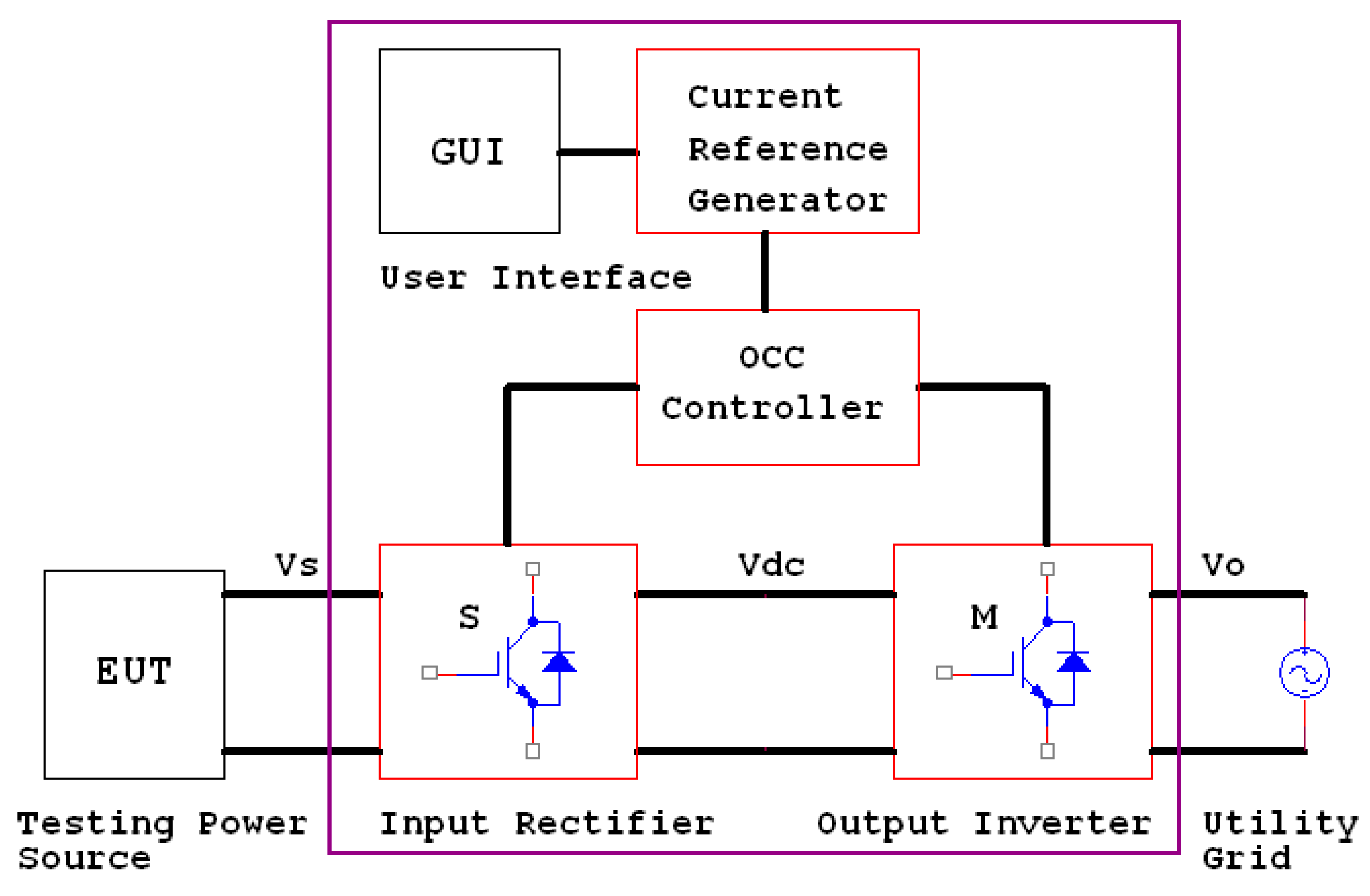
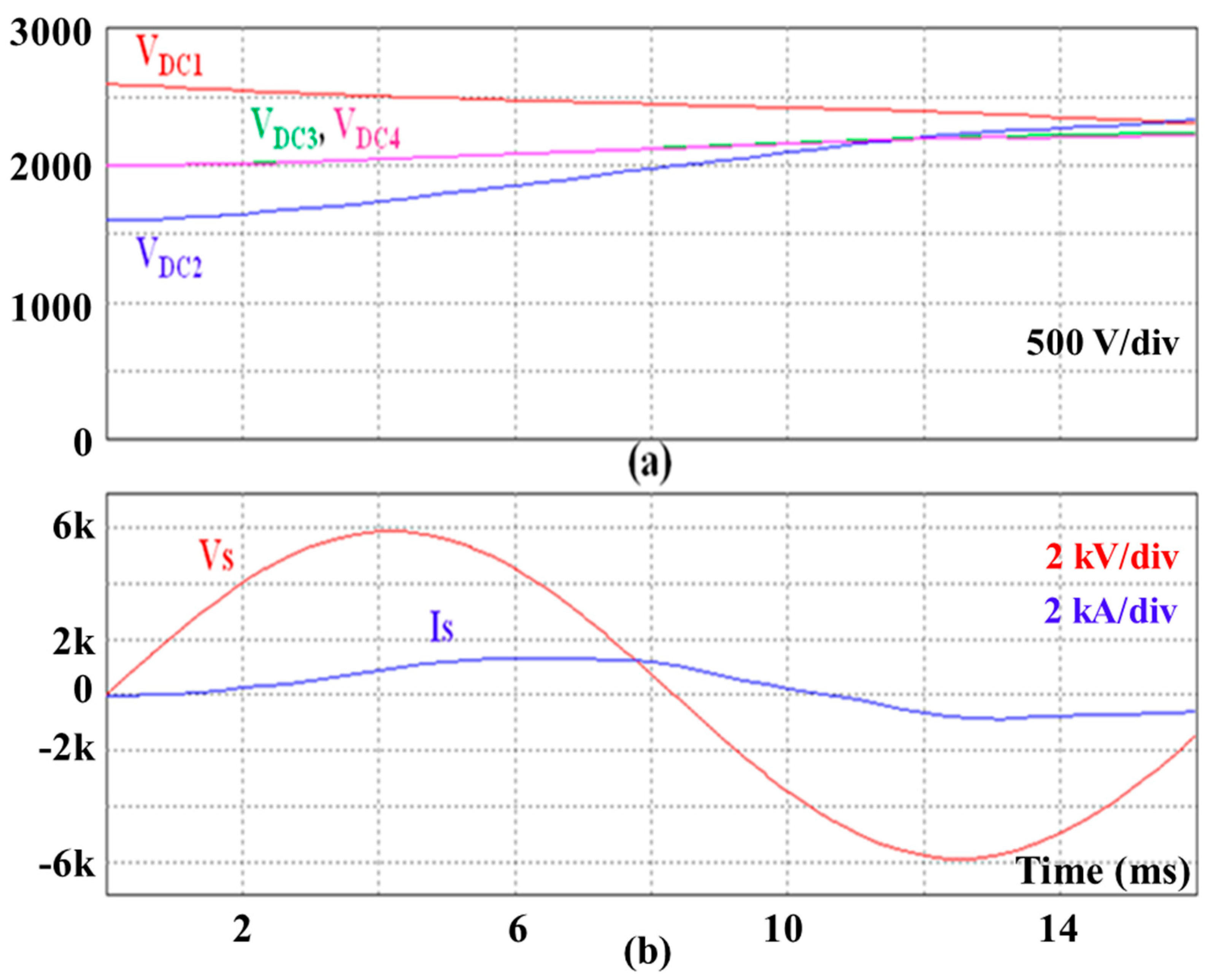
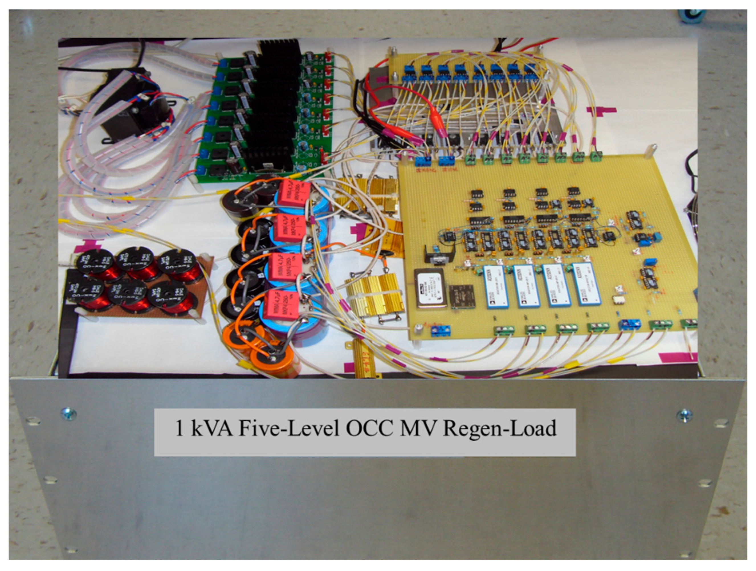
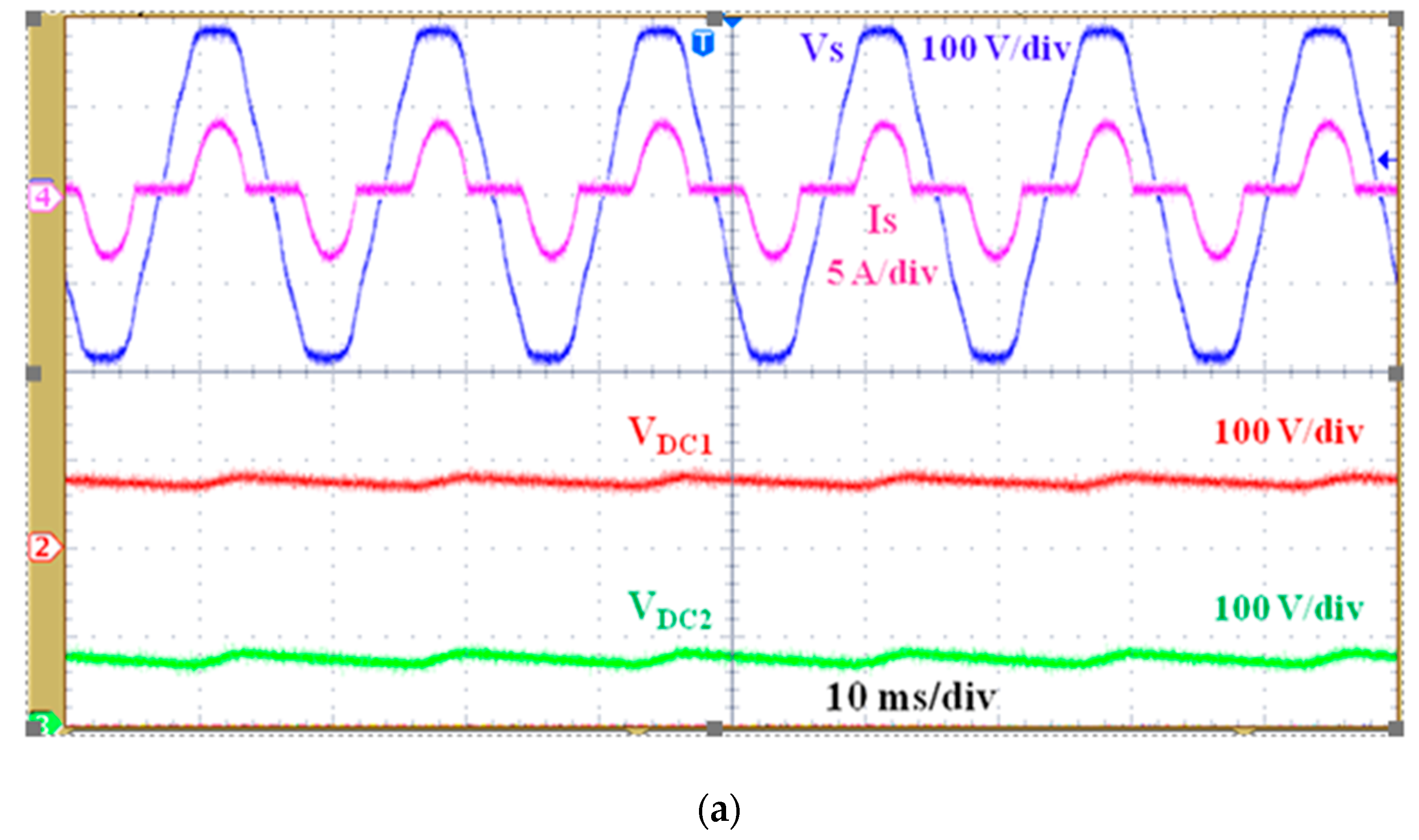
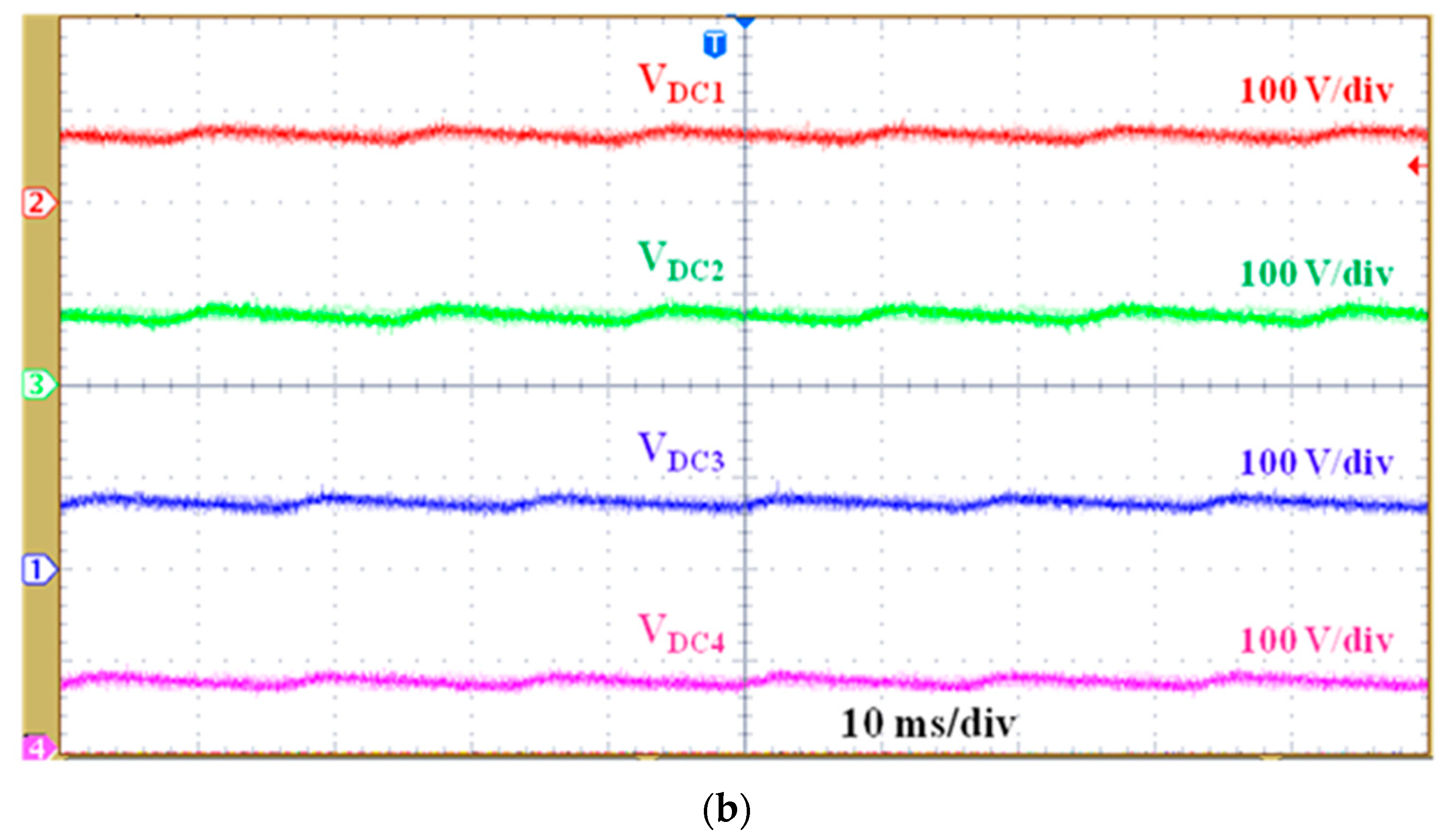
This paper presents a five-level DCMC-based MV regenerative AC electronic load (MV Regen-Load) with four-carrier level-shifted OCC control based on back-to-back configuration targeted towards high power MV applications, with the capability of emulating various impedance loads. A small-scale prototype of 1 kVA 120 Vac five-level OCC MV Regen-Load was designed and tested to verify the performance of the proposed five-level OCC MV Regen-Load. The regenerative feature of the proposed MV Regen-Load provides an effective energy saving solution for MV power equipment testing since the testing energy is fed back to the grid instead of being dissipated as heat during operation. In this paper, especially the dc-link voltage balancing control of the proposed five-level MV Regen-Load by using the simple level-shifted OCC is deeply analyzed. Compared to the conventional level-shifted SPWM control, the proposed level-shifted OCC of the five-level DCMC-based MV Regen-Load has the variable amplitudes of four carrier signals instead of the fixed amplitudes. With variable amplitude control of the four carrier signals, the dc-link capacitor voltages automatically become balanced and equal to the reference voltage (VDC/4). The most important merit of the proposed multilevel OCC method is to reduce a heavy computing burden. Simulation and experiments were performed using small-scale five-level DCMCs to verify the proposed multilevel MV Regen-Load performance.

2. Multilevel OCC MV Regenerative Load Configuration

Figure 1 shows the diagram of the proposed single-phase multilevel MV Regen-Load. It is composed of a multilevel input rectifier, a multilevel output inverter, an OCC controller, a current reference generator and a graphical user interface (GUI). The equipment under test (EUT) is connected to the multilevel input rectifier, which is connected to the multilevel output inverter in a back-to-back configuration to realize energy regeneration to the power grid. The current reference generator produces the current reference signal for the proposed OCC controller to emulate the user-defined linear or nonlinear load. The GUI helps the user set up any load condition and provides the user-defined modeling option for complicated or dynamic loads.
The power stage topology of the single-phase five-level MV Regen-Load is shown in Figure 2. The five-level input rectifier emulates the specified impedance while the five-level output inverter sends the absorbed energy back to the utility grid with unit power factor. The multilevel OCC MV Regen-Load is capable of emulating a specified load for the EUT by controlling the amplitude and phase of the input current of the multilevel MV Regen-Load. In addition, the proposed multilevel MV Regen-Load can be used in dynamic load emulation with fast and accurate response, due to the inherent characteristics of the OCC. Theoretically, when all components are ideal, the OCC MV Regen-load has no loss. Practically, certain percentage of energy is lost as conduction loss and switching loss. Typically, the loss will be round 5%, which is a significant improvement over the conventional 100% loss.

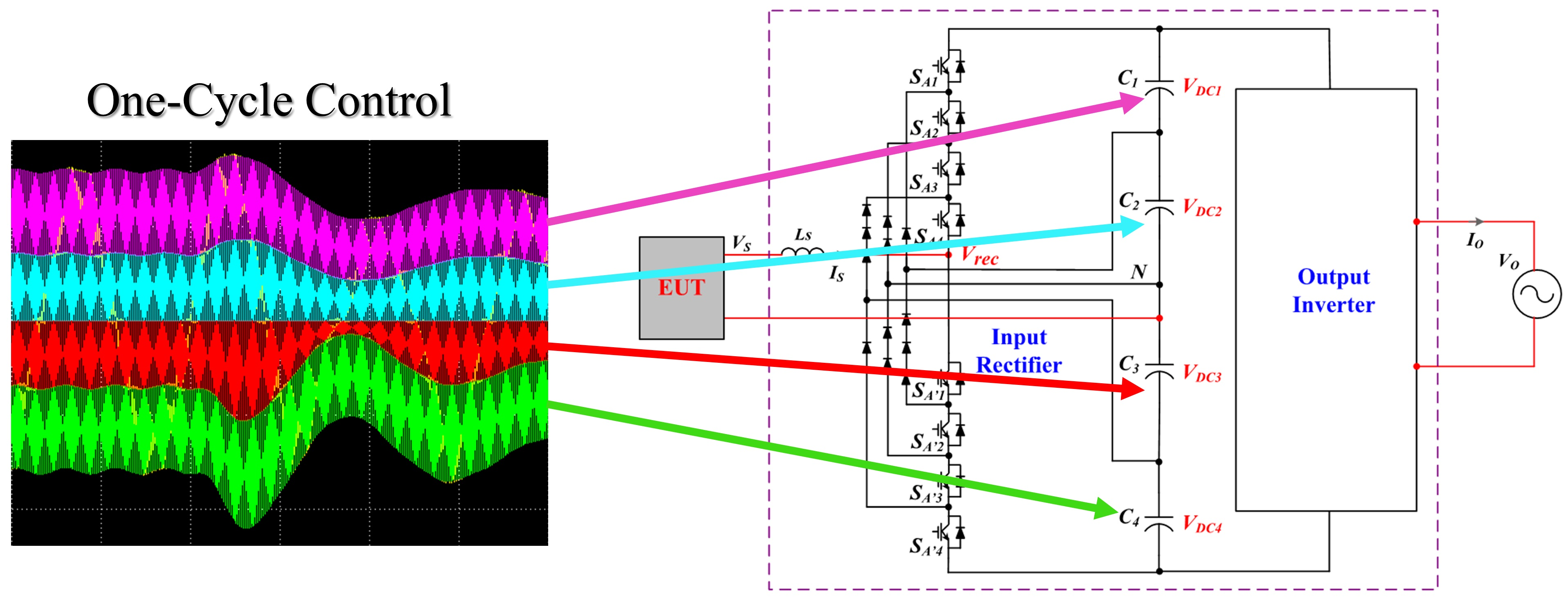
3. OCC Control of Five-Level Regen-Load
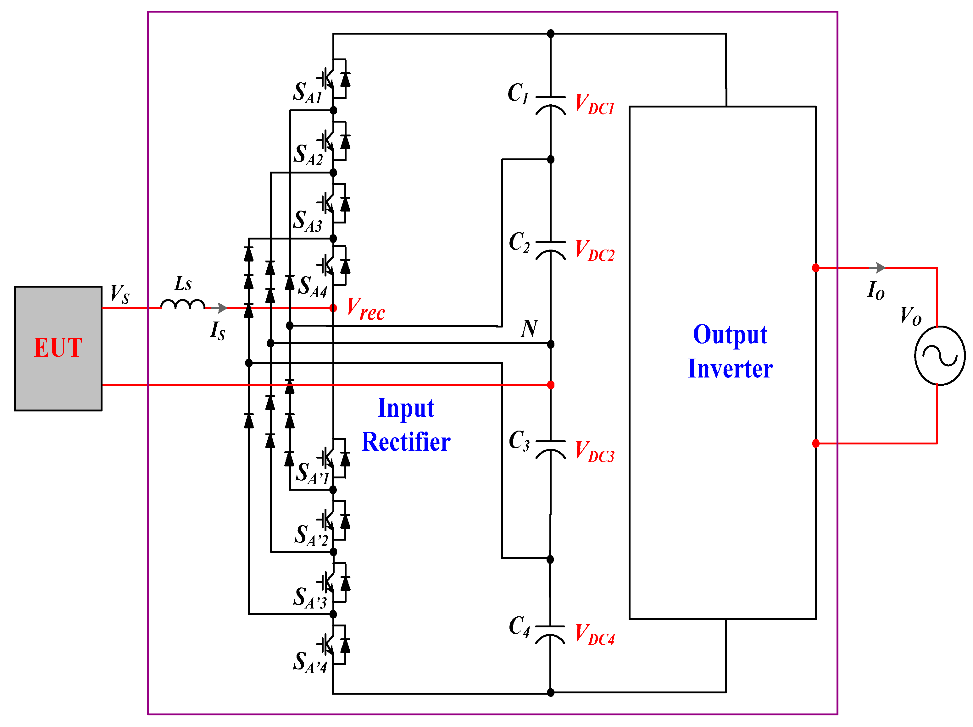
As shown in Figure 2, the five-level DCMC is comprised of eight active switches (SA1SA’4), 12 clamping diodes, four dc-link capacitors and an input inductor (LS). Voltage sharing between the main switches is achieved by the clamping diodes. It has been a major challenge to balance the dc-link capacitor voltages in a multilevel converter, especially as the number of levels increases. Traditionally two types of balancing methods were reported: using the redundant switching states and using the auxiliary balancing circuits.
With the SVPWM control, a number of redundant switching states can be used to help balance the dc-link capacitor voltages. This approach may minimize or eliminate the need for auxiliary balancing circuits. However, for five or higher-level multilevel converters, the SVPWM control is computation intensive and not commonly used in industrial applications. For example, a five-level multilevel converter has 53 = 125 switching states, for which the computation burden may require high-speed DSPs, limit the maximum switching frequency or slow down control response. In addition, the use of redundant switching states increases the switching frequency and the switching loss which is undesired for practical applications.
On the other hand, the traditional carrier-based SPWM control of the DCMCs produces unbalanced dc-link capacitor voltages. Thus, a balancing circuit is generally required, which significantly increases the complexity of the multilevel converter circuits or systems.
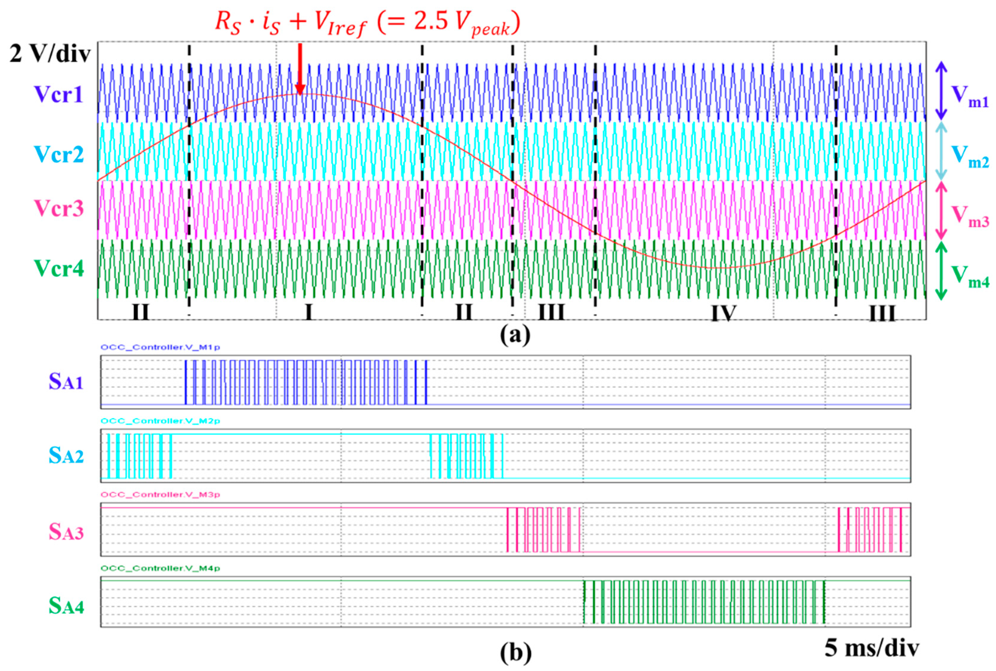
The proposed level-shifted OCC method provides a simple approach to balance the dc-link capacitor voltages for multilevel converters without involving any auxiliary balancing circuit. For the five-level DCMC, four-carrier level-shifted SPWM with variable carrier-amplitude control is employed as shown in Figure 3a. In general, the four carriers can be arranged in different forms: phase disposition (PD), phase opposition disposition (POD) and alternative phase opposition disposition (APOD). Among the above carrier forms, the PD technique, where all carriers are in phase, provides the lowest harmonic distortion.
Based on the level-shifted PD SPWM control, the four carrier signals (Vcr1–Vcr4) of the proposed five-level OCC MV Regen-Load have the same phase but different amplitudes, depending on each dc-link capacitor voltage (VDC1, … VDC4).
Figure 3 shows the single-phase OCC MV Regen-Load PWM waveforms of the five-level DCMC input rectifier. In Figure 3a, a sinusoidal reference (RS·IS + VIref) is compared with the four carrier signals (Vcr1–Vcr4) to determine the switched voltage levels: +VDC/2 (+ VDC1 + VDC2), +VDC/4 (+VDC2), 0, −VDC/4 (−VDC3) and −VDC/2 (−VDC3VDC4). The line period is divided into four operation regions, according to where the reference signal lands, named as I, II, III and IV. The five-level DCMC input rectifier assumes different equivalent circuits and switching states in a different operation region.
Table 1 shows the five-level DCMC input rectifier voltages (Vrec or Vrec–N) and their switching states. The eight active switches are controlled as complementary pairs (SA1, SA’1, etc.). In region I in Figure 3a, the input rectifier voltage is switched between VDC1 + VDC2 and VDC2 by the first upper switch SA1 and its complementary switch SA’1. As shown in Figure 3b, the other upper switches (SA2SA4) are kept on in region I. Similarly, in region II, the second upper switch SA2 and its complementary switch SA’2 are switched to provide the input rectifier voltage between VDC2 and 0. In this region, the first upper switch SA1 is turned off, and the other two upper switches (SA3, SA4) are always turned on to provide the neutral point connection (0 or N) in Figure 2. For region III and IV, the same switching approach is applied to produce the negative input rectifier voltages.
Assuming that the proposed OCC MV Regen-Load operates in continuous conduction mode, the equivalent circuits and the OCC control equations can be found for four operation regions. Figure 4 shows the simplified equivalent circuit of the five-level OCC MV Regen-Load in region I. By applying the volt-second balance rule to the input inductor (LS), the conversion gain equation for the equivalent circuit in Figure 4 can be derived by (1):
V S = V D C 2 + V D C 1 d S A 1 V D C 4 ( 1 + d S A 1 )
where dSA1 is the duty ratio of the first upper switch SA1.
Then, the control goal of the OCC MV Regen-Load is for the input current (iS) to track the current reference signal (VIref). According to this condition, the control goal can be defined by the Norton equivalent circuit as follows:
V S = R E ( i S + I S r e f )
where RE is the emulated resistance of the input rectifier and ISref is the input current reference.
By combining the conversion gain Equation (1) and the control goal (2), the control key equation for the OCC MV Regen-Load in region I can be derived by the Thévenin equivalent circuit as follows:
R S i S + V I r e f = V m 2 + V m 1 d S A 1
where RS is the sensing resistance of the input current, VIref is the current reference signal, Vm1Vm2 are the carrier amplitudes, V I r e f = R S I S r e f , V m 1 = V D C 1 R S R E and V m 2 = V D C 2 R S R E .
With a similar procedure, the control key equations for the other operation regions can be derived in Table 2.
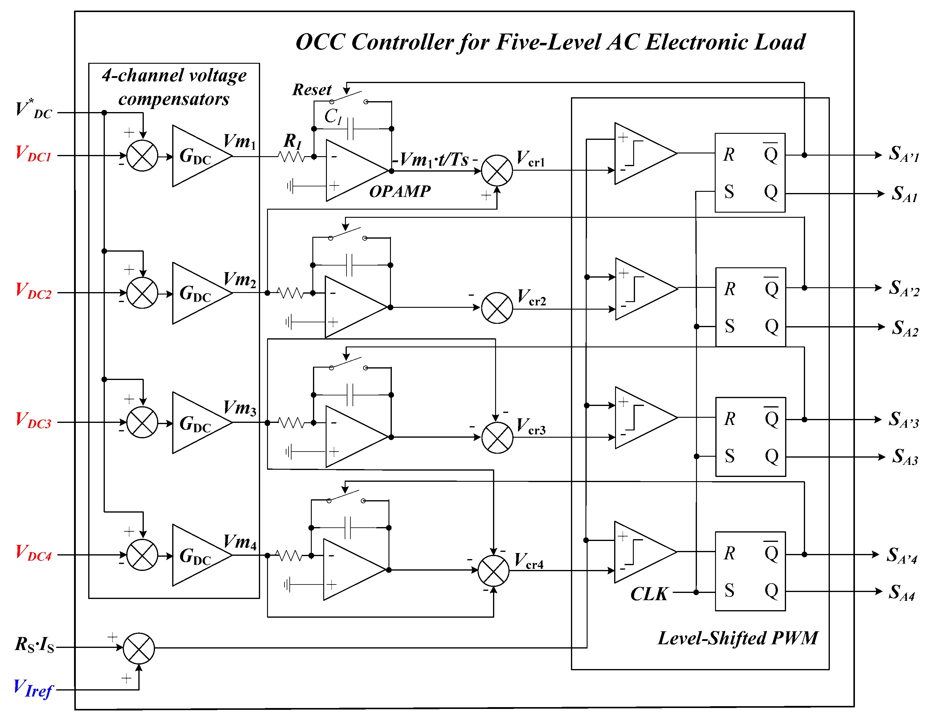
To implement all the control key equations, an OCC level-shifted PWM control circuit is proposed shown in Figure 5, using a clock signal (CLK), four integrators, four comparators, four RS flip-flops and four reset switches for PWM generation. The OCC level-shifted PWM control circuit of the five-level OCC MV Regen-Load consists of four voltage compensators and OCC level-shifted PWM generators for the eight gate signals (SA1SA’4). The four identical voltage compensators determine the carrier amplitudes (Vm1Vm4), depending on deviation of each dc-link capacitor voltage (VDC1VDC4) from the reference voltage V*DC (= VDC/4). Using four integrators and three adders, the level-shifted carrier signals (Vcr1–Vcr4) are generated with the different amplitudes and dc-level shifts. By comparing the control reference (RS·IS + VIref) with the four carrier signals (Vcr1–Vcr4), the actual gate signals are produced by the RS flip-flops. When both the input signals of each comparator approach one another, the comparator changes its state, which in turn resets the RS flip-flop through its ‘R’ input terminal and its integrator to zero. The next clock signal (CLK) sets the RS flip-flop through its ‘S’ input terminal and the output terminal ‘Q’ of the RS flip-flop is also set, which turns on its gate signal (SA1SA4). With variable amplitude control of the four carrier signals, the dc-link capacitor voltages can become balanced and equal to the reference voltage (VDC/4) even under different dc-link capacitances (C1C4).
The input current of the five-level DCMC input rectifier of the OCC MV Regen-Load accurately tracks the current reference signal and to realize the specified impedance load. For the proposed OCC MV Regen-Load, the control of the input rectifier is the key point. For the five-level DCMC output inverter of the OCC MV Regen-Load, the control goal is to make the output current IO of the OCC MV Regen-Load synchronous with the grid voltage VO and contribute to the unit power factor injection of the recycled testing energy with the highest efficiency. In this condition, the control requirement is to realize unit power factor operation and stabilize the dc-link voltage. A multilevel converter similar to the input rectifier can be used to implement the inverter. Due to the similarity of the topology and for the purpose of simplicity but without loss of the generality, the discussion of the multilevel inverter is kept brief.

4. DC-Link Capacitor Voltage Balance Analysis

For the DCMCs, a major challenge is to keep all dc-link capacitor voltages balanced, which was usually achieved with an extra voltage-balancing circuitry or a specific voltage-balancing control previously.
In this section, the dc-link capacitor voltage balance issue for the five-level OCC MV Regen-Load is analyzed based on the proposed level-shifted OCC control. 
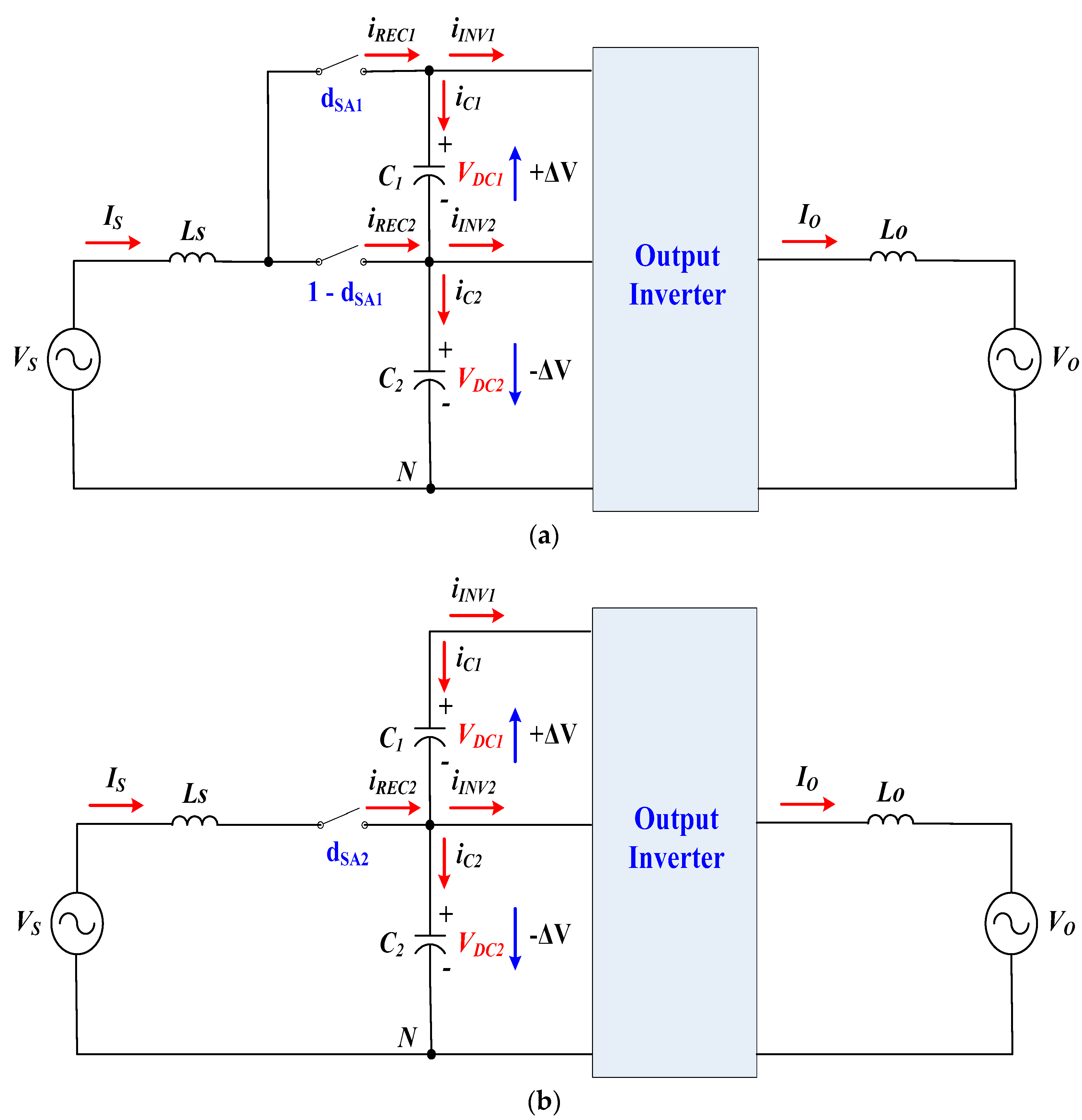
Figure 6 shows the dc-link currents of the five-level OCC MV Regen-Load in region I and II when the control reference (RS·IS + VIref) is positive during the half-cycle of the input line frequency. In region I and II, the two upper switches (SA1, SA2) are modulated, respectively, and the two upper dc-link capacitors (C1, C2) are also charged or discharged, respectively, depending on the load emulation and each dc-link capacitor voltage. When the control reference is negative in region III and IV, the other upper two switches (SA3, SA4) are switched, respectively, with the two lower dc-link capacitors (C3, C4), and the related PWM control and the dc-link voltage-balancing method in region III and IV are the same as those in region I and II. For proper operation of the five-level OCC MV Regen-Load, the amplitudes and dc-level shifts of the four carrier signals (Vcr1–Vcr4) must be properly controlled to achieve dc-link voltage balancing.
Figure 7 shows the simplified equivalent circuit models of the five-level OCC MV Regen-Load in region I and II, respectively. From Figure 7a, the two dc-link capacitor currents (iC1, iC2) in region I can be described by the following expressions:
i C 1 = C 1 d V D C 1 d t = i R E C 1 i I N V 1 = d S A 1 ( i S + I S r e f ) i I N V 1
i C 2 = C 2 d V D C 2 d t = i C 1 + i R E C 2 i I N V 2 = ( i S + I S r e f ) ( i I N V 1 + i I N V 2 )
Similarly, the two dc-link capacitor currents in region II, which are shown in Figure 7b can be expressed as:
i C 1 = C 1 d V D C 1 d t = i I N V 1
i C 2 = C 2 d V D C 2 d t = i C 1 + i R E C 2 i I N V 2 = d S A 2 ( i S + I S r e f ) ( i I N V 1 + i I N V 2 )
Assuming that the four dc-link capacitors (C1C4) have the same capacitance, when a disturbance causes imbalance in the two upper dc-link capacitor voltages (e.g., VDC1 > V*DC > VDC2), a state variable ∆V is defined as half the difference between the two upper dc-link capacitor voltages (VDC1, VDC2), which should converge to zero with the proposed level-shifted OCC control. In the unbalanced condition, each dc-link capacitor voltage can be defined as a function of the voltage difference ∆V by:
V D C 1 = V C + Δ V
V D C 2 = V C Δ V
where
V C = V D C 1 + V D C 2 2
Δ V = V D C 1 V D C 2 2
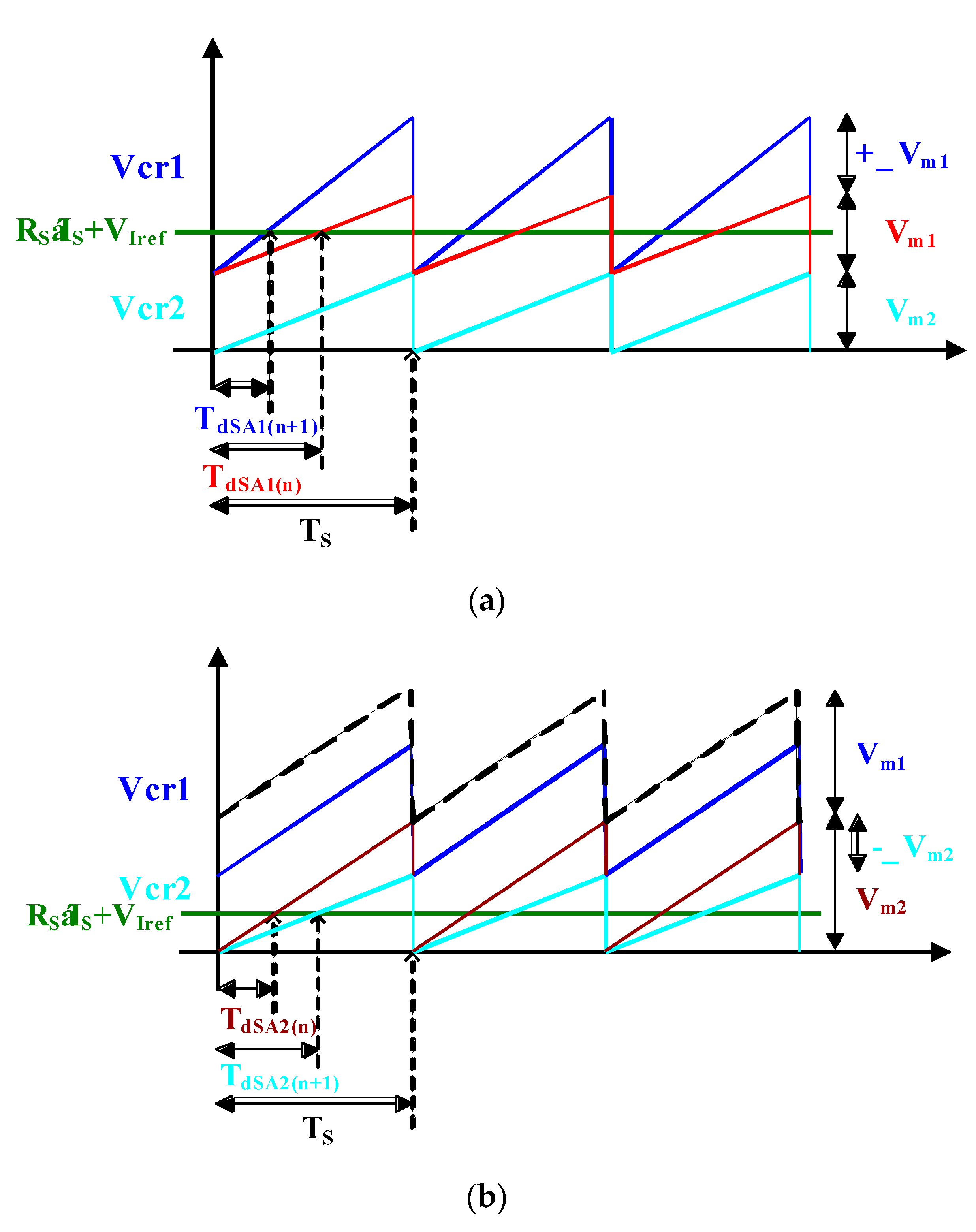
In order to maintain the dc-link capacitor voltage balance, the proposed control of the five-level OCC MV Regen-Load in region I and II is shown in Figure 8. From Figure 8a, the duty ratios of the SA1 switch under an unbalanced dc-link condition can be described as follows:
d S A 1 ( n ) = T d S A 1 ( n ) T S = R S i S + V I r e f V m 2 V m 1
d S A 1 ( n + 1 ) = T d S A 1 ( n + 1 ) T S = R S i S + V I r e f ( V m 2 Δ V m 2 ) V m 1 + Δ V m 1
where dSA1(n) and dSA1(n + 1) are the duty ratios of the SA1 switch at the (n)th and (n + 1)th switching cycles, and:
V m 1 = V D C 1 R S R E
Δ V m 1 = R S R E Δ V D C 1 = R S R E Δ V
From (8) and (9), the duty ratio variation of the SA1 switch (∆dSA1) to compensate the unbalanced dc-link capacitor voltages can be obtained by:
Δ d S A 1 = d S A 1 ( n + 1 ) d S A 1 ( n ) = Δ V D C 1 ( n ) [ R E ( i S + I S r e f ) + V D C 2 ( n ) ] + Δ V D C 2 ( n ) V D C 1 ( n ) V D C 1 ( n ) ( V D C 1 ( n ) + V D C 2 ( n ) ) V D C 1 ( n ) ( V D C 1 ( n ) + Δ V D C 1 ( n ) )
Assuming VDC1(n) >> ∆VDC1(n), the above equation can be simplified as:
Δ d S A 1 = Δ V D C 1 ( n ) V D C 1 ( n ) 2 [ R E ( i S + I S r e f ) + V D C 2 ( n ) ] + Δ V D C 2 ( n ) V D C 1 ( n ) ( V D C 1 ( n ) + V D C 2 ( n ) ) V D C 1 ( n )
From (4) and (11), it is possible to define the relationship between the duty ratio variation of the Vcr1 carrier signal and the compensation for the dc-link capacitor voltage unbalance. The voltage variations of the two upper dc-link capacitors (C1, C2) in region I are given by:
Δ V D C 1 ( n + 1 ) = T S C 1 V D C 1 ( n ) 2 [ R E ( i S + I S r e f ) + V D C 2 ( n ) ] ( i S + I S r e f ) Δ V D C 1 ( n ) + T S C 1 V D C 1 ( n ) ( i S + I S r e f ) Δ V D C 2 ( n ) T S C 1 V D C 1 ( n ) ( V D C 1 ( n ) + V D C 2 ( n ) ) ( i S + I S r e f ) T S C 1 Δ I I N V 1 = A 1 Δ V D C 1 ( n ) + A 2 Δ V D C 2 ( n ) + A C 1 + A C 2
Δ V D C 2 ( n + 1 ) = T S C 2 ( Δ I I N V 1 Δ I I N V 2 ) = B C 1 + B C 2
When VDC1 > V*DC > VDC2, ∆dSA1 is negative and ∆IINV1 is positive in region I. Therefore, the over-charged C1 capacitor voltage (VDC1) will decrease and the under-charged or over-discharged C2 capacitor voltage (VDC2) will increase to reduce the dc-link capacitor voltage deviation, depending on the difference between ∆IINV1 and ∆IINV2.
Since ∆VDC1(n) – ∆VDC1(n + 1) = (1 – A1) · ∆VDC1(n)A2·VDC2(n)AC1AC2 > 0, the following compensation control is obtained:
Δ V D C 1 ( n + 1 ) Δ V D C 1 ( n ) < 1
In this unbalanced condition, ∆VDC1 is decreasing during each switching cycle to reach the nominal dc-link capacitor voltage. From Figure 8b, similarly, the duty ratios of the SA2 switch under an unbalanced dc-link condition can be described as follows:
d S A 2 ( n ) = T d S A 2 ( n ) T S = R S i S + V I r e f V m 2
d S A 2 ( n + 1 ) = T d S A 2 ( n + 1 ) T S = R S i S + V I r e f V m 2 Δ V m 2
where dSA2(n) and dSA2(n + 1) are the duty ratios of the SA2 switch at the (n)th and (n + 1)th switching cycles, and:
V m 2 = V D C 2 R S R E
Δ V m 2 = R S R E Δ V D C 2 = R S R E Δ V
From (14) and (15), the duty ratio variation of the SA2 switch (∆dSA2) to adjust the unbalanced dc-link capacitor voltages can be obtained by:
Δ d S A 2 = d S A 2 ( n + 1 ) d S A 2 ( n ) = Δ V D C 2 ( n ) R E ( i S + I S r e f ) V D C 2 ( n ) ( V D C 2 ( n ) Δ V D C 2 ( n ) )
Assuming VDC2(n) >> ∆VDC2(n), the duty ratio variation of the SA2 switch can be simplified as:
Δ d S A 2 = d S A 2 ( n + 1 ) d S A 2 ( n ) = Δ V D C 2 ( n ) V D C 2 ( n ) 2 R E ( i S + I S r e f )
From (5) and (17), the voltage variations of the two upper dc-link capacitors (C1, C2) in region II are given by:
Δ V D C 1 ( n + 1 ) = T S C 1 ( Δ I I N V 1 ) = A C 2
Δ V D C 2 ( n + 1 ) = T S C 2 V D C 2 ( n ) 2 R E ( i S + I S r e f ) 2 Δ V D C 2 ( n ) T S C 2 ( Δ I I N V 1 + Δ I I N V 2 ) = B 2 Δ V D C 2 ( n ) + B C 1 + B C 2
When VDC1 > V*DC > VDC2, ∆dSA2 is positive and ∆IINV1 is also positive in region II, the over-charged C1 capacitor voltage (VDC1) will decrease and the under-charged C2 capacitor voltage (VDC2) will increase to eliminate the dc-link capacitor voltage deviation.
Finally, the voltage variations of the four dc-link capacitors (C1C4) can be described as follows:
[ Δ V D C 1 ( n + 1 ) Δ V D C 2 ( n + 1 ) Δ V D C 3 ( n + 1 ) Δ V D C 4 ( n + 1 ) ] = [ T S C 1 V D C 1 ( n ) 2 [ R E ( i S + I S r e f ) + V D C 2 ( n ) ] ( i S + I S r e f ) T S C 1 V D C 1 ( n ) ( i S + I S r e f ) 0 0 0 T S C 2 V D C 2 ( n ) 2 R E ( i S + I S r e f ) 2 0 0 0 0 T S C 3 V D C 3 ( n ) 2 R E ( i S + I S r e f ) 2 0 0 0 T S C 4 V D C 4 ( n ) ( i S + I S r e f ) T S C 4 V D C 4 ( n ) 2 [ R E ( i S + I S r e f ) + V D C 3 ( n ) ] ( i S + I S r e f ) ] · [ Δ V D C 1 ( n ) Δ V D C 2 ( n ) Δ V D C 3 ( n ) Δ V D C 4 ( n ) ] + [ T S C 1 V D C 1 ( n ) ( V D C 1 ( n ) + V D C 2 ( n ) ) ( i S + I S r e f ) T S C 1 Δ I I N V 1 T S C 2 Δ I I N V 1 T S C 2 Δ I I N V 2 T S C 3 Δ I I N V 3 T S C 3 Δ I I N V 4 T S C 4 V D C 4 ( n ) ( V D C 3 ( n ) + V D C 4 ( n ) ) ( i S + I S r e f ) T S C 4 Δ I I N V 4 ] = [ A 1 A 2 0 0 0 B 2 0 0 0 0 C 3 0 0 0 D 3 D 4 ] · [ Δ V D C 1 ( n ) Δ V D C 2 ( n ) Δ V D C 3 ( n ) Δ V D C 4 ( n ) ] + [ A C 1 + A C 2 B C 1 + B C 2 C C 1 + C C 2 D C 1 + D C 2 ] = [ A 1 A 2 0 0 0 B 2 0 0 0 0 C 3 0 0 0 D 3 D 4 ] · [ Δ V D C 1 ( n ) Δ V D C 2 ( n ) Δ V D C 3 ( n ) Δ V D C 4 ( n ) ] + [ A C B C C C D C ]
Using (19), the voltage variation vector ΔVDC(n) can be written by a 4 × 4 matrix A and the initial voltage variation vector ΔVDC(0):
Δ V D C ( n ) = [ Δ V D C 1 ( n ) Δ V D C 2 ( n ) Δ V D C 3 ( n ) Δ V D C 4 ( n ) ] = A [ Δ V D C 1 ( n 1 ) Δ V D C 2 ( n 1 ) Δ V D C 3 ( n 1 ) Δ V D C 4 ( n 1 ) ] + B = A n [ Δ V D C 1 ( 0 ) Δ V D C 2 ( 0 ) Δ V D C 3 ( 0 ) Δ V D C 4 ( 0 ) ] + C = A n Δ V D C ( 0 ) + C
where:
A n = [ A 1 n ( A 1 n 1 + A 1 n 2 B 2 + + A 1 B 2 n 2 + B 2 n 1 ) A 2 0 0 0 B 2 n 0 0 0 0 C 3 n 0 0 0 ( C 3 n 1 + C 3 n 2 D 4 + + C 3 D 4 n 2 + D 4 n 1 ) D 3 D 4 n ] and   C = [ A n + A n 1   + + A + I ] · B
From (19)–(21), it is clear that the voltage variations of the four dc-link capacitors become zero in steady state, even though there are some voltage variations of the dc-link capacitors in the beginning or induced by some perturbation. Based on the proposed level-shifted OCC control, dc-link capacitor voltage balance can be achieved for any load emulation condition. It is also clear that the stabilizing time required to eliminate the dc-link voltage unbalance is proportional to the dc-link capacitance and inversely proportional to the amplitude of the input current.

5. Simulation and Experimental Results

5.1. Simulation Results

A single-phase five-level OCC MV Regen-Load has been simulated using PSIM to verify the steady and dynamic performance. In the simulation, the input line voltage (VS) is 4.16 kVac and the input inductor (LS) is 2.8 mH. The input line frequency is 60 Hz and the carrier frequency is 5 kHz. In addition, the main switches SA1SA’4 have 2.5 V saturation voltage and 2.5 V reverse diode voltage drop. The diode voltage drop of the clamping diodes is also 2.5 V. All the parameters of the simulation system are shown in Table 3.
In this simulation, the nominal dc-link capacitor voltage (V*DC) is 2.25 kVdc.
Figure 9 shows the two upper dc-link capacitor voltages (VDC1, VDC2) and the related upper carrier signals (Vcr1, Vcr2) to compensate the initial dc-link capacitor voltage unbalance (VDC1 > VDC2). In the simulation, the initial VDC1 is 2.6 kVdc and the initial VDC2 is 1.6 kVdc. In region I and II, the amplitudes of the Vcr1 and Vcr2 carrier signals can be decided by the deviation levels from the reference voltage (V*DC), respectively. For the Vcr1 carrier signal, its carrier amplitude is smaller than the Vcr2 carrier signal since the initial C1 capacitor voltage (VDC1) has less deviation level than the C2 capacitor voltage (VDC2). Depending on the operation condition, the minimum carrier amplitude should be properly designed to control the compensation time for the dc-link capacitor voltage unbalance.
Figure 10 shows the dc-link capacitor voltages (VDC1VDC4) and the input line waveforms (VS, IS) for the five-level OCC MV Regen-Load when the initial dc-link capacitor voltages are unbalanced (VDC1 > V*DC > VDC3 = VDC4 > VDC2). In Figure 10a, the two upper dc-link capacitor voltages (VDC1, VDC2) have different initial values. In this case, the initial VDC1 is 2.6 kVdc and the initial VDC2 is 1.6 kVdc. On the other hand, the two lower dc-link capacitors (C3, C4) have the same initial values (VDC3 = VDC4 = 2 kVdc). From Figure 10a, it is clear that the dc-link voltage balancing can be achieved within the single cycle of the input line voltage under the unbalanced initial condition. Figure 10b shows the input line voltage and input line current waveforms for an inductive load emulation. The input line current (IS) has about 1 kA peak amplitude and +30° phase lag with the input line voltage, working as a 30° RL load. As shown in Figure 10, the five-level OCC MV Regen-Load has the capability to emulate any high voltage and high current load condition with full control of the dc-link voltage balancing over all the operating conditions.
From this simulation, each dc-link capacitor voltage VDC1VDC4 is 4 kVdc to compare the normal operation of the proposed five-level OCC MV Regen-Load under different dc bus voltage condition.
Figure 11 shows the simulation waveforms of the proposed five-level OCC MV Regen-Load for a resistive load emulation. The input line voltage vs. and the input current IS with about 400 A peak amplitude are in phase to represent the resistor load condition–17 Ω in this case. As expected, the input rectifier has five voltage levels (Vrec) from +VDC/2 to −VDC/2 and is also in phase with the input line current IS.
Figure 12 shows the proposed five-level OCC MV Regen-Load waveforms for an inductive load emulation when the current reference signal VIref has 2 V amplitude and −60° phase angle. In Figure 12a, the input line current IS has about 200 A peak amplitude with +60° phase delay, compared to the input line voltage VS. Similarly, the five-level rectifier voltage has 60° phase shift with the input line current, working as a 60° RL load. From the fast fourier transform (FFT) of the PSIM, the total harmonic distortion (THD) of the five-level rectifier voltage without filters is about 24%. The generated harmonic distortion can be reduced by employing proper passive or active filters.
Figure 13 shows the voltage and current waveforms for a diode rectifier load emulation when the proposed five-level OCC MV Regen-Load emulates a nonlinear rectified load with a diode bridge rectifier, a 0.5 mH dc link inductor, a 10 mF dc-link capacitor and a 100 Ω resistor load. In this test condition, the THD of the input current is about 41.5% from the diode rectifier load.

5.2. Experimental Results

To verify the performance of the proposed five-level OCC MV Regen-Load, a small-scale prototype of 1 kVA 120 Vac five-level OCC MV Regen-Load was built in Figure 14, using IGBTs (IRGP4072DPbF), diodes (MUR1540G) and 2.5 A IGBT driver (VO3120) with optical isolation. A magneto-resistive current sensor (NT-5) is used to read the input line current IS and a hall-effect voltage sensor (LV25-P) is applied to read the input line voltage VS. For dc-link voltage measurement, four isolation amplifiers (AD202KN) are used to read each dc-link capacitor voltage (VDC1VDC4). The input line voltage vs. and the output grid voltage VO have the same amplitude, 120 Vac with variable transformers. The dc-link voltage VDC is 400 Vdc and each dc-link capacitor (C1C4) is 1800 µF. In the input rectifier, the input inductor LS is 2.8 mH and the carrier frequency is 5 kHz. All the parameters of the experimental system are shown in Table 4.
Figure 15 shows the experimental result for the dc-link voltage balancing of the proposed five-level OCC MV Regen-Load. In Figure 15a, when the five-level OCC MV Regen-Load emulates the diode rectifier load with about 4 A peak amplitude, the two upper dc-link capacitor voltages (VDC1, VDC2) are regulated under the dc-link balancing condition. Since a variable transformer is used between the power grid and the five-level OCC MV Regen-Load for safety, the input voltage shows somewhat saturated waveform around its peak values but is acceptable by the Standard. As shown in Figure 15b, the four dc-link capacitor voltages (VDC1VDC4) are also balanced by the proposed level-shifted OCC PWM control with variable carrier amplitudes.
Figure 16 shows the experimental result for regenerative operation of the proposed five-level OCC MV Regen-Load. The input rectifier with about 4 A peak input current emulates a RC load and the output inverter feeds back the absorbed testing energy to the power grid as seen in Figure 16. The THD is less than 5% at 60 Hz output frequency and the efficiency is about 88%.

6. Conclusions

In this paper, OCC control method is extended for multilevel DCMCs that features a simple control circuit and automatic dc-link voltage balancing. Based on the OCC control, the five-level OCC MV Regen-Load is proposed to emulate linear or nonlinear load and in the meantime recycle the testing energy back to the power grid. The proposed OCC MV Regen-Load is based on back-to-back five-level DCMCs and four-carrier level-shifted OCC PWM control for the single-phase or three-phase configuration. With the proposed level-shifted OCC control, the voltage balancing of the dc-link capacitors for the back-to-back five-level DCMCs is automatically achieved without the need of additional balancing circuitry. The proposed five-level OCC MV Regen-Load can emulate any RLC, diode rectifier load and their combinations for MV applications.
The proposed OCC voltage-balancing technique of the dc-link capacitors is capable of keeping the dc-link capacitor voltages balanced even when the four dc-link capacitors have different capacitance or initial voltage condition. Simulation and experimental results have verified the dc-link voltage balance performance of the proposed five-level OCC MV Regen-Load based on back-to-back configuration. The experimental results based on the 1 kVA 120 Vac small-scale prototype also show that the proposed five-level OCC MV Regen-Load returns about 88% of the testing energy back to the power grid thereby providing significant electrical savings, where the design target is greater than 90%. The proposed five-level OCC MV Regen-Load is very suitable for performance validation, burn-in, life-time test, etc. of MV electrical machines, wind turbine generators and other AC power equipment with convenient dial-in of the impedance type and value.

Funding

This research received no external funding.

Acknowledgments

This work was supported by the Korea Institute of Energy Technology Evaluation and Planning (KETEP) and the Ministry of Trade, Industry and Energy (MOTIE) of the Republic of Korea. (No. 20206310100220).

Conflicts of Interest

The author declares no conflict of interest.

Abbreviations

The following abbreviations are used in this manuscript:
MVMedium voltage
DCMCDiode-clamped multilevel converter
SVPWMSpace vector pulse width modulation
DSPDigital signal processor
IGBTInsulated gate bipolar transistor
MV Regen-LoadMV regenerative AC electronic load
OCCOne-cycle control
PFCPower factor correction
APFActive power filter
GUIGraphical user interface
EUTEquipment under test
PDPhase disposition
PODPhase opposition disposition
APODAlternative phase opposition disposition
CLKClock signal
FFTFast fourier transform
THDTotal harmonic distortion

References

  1. Chroma. Available online: www.chromausa.com (accessed on 23 September 2021).
  2. Hatti, N.; Kondo, Y.; Akagi, H. Five-Level Diode-Clamped PWM Converters Connected Back-to-Back for Motor Drives. IEEE Trans. Ind. Appl. 2008, 44, 1268–1276. [Google Scholar] [CrossRef]
  3. Shu, Z.; He, X.; Wang, Z.; Qiu, D.; Jing, Y. Voltage Balancing Approaches for Diode-Clamped Multilevel Converters Using Auxiliary Capacitor-Based Circuits. IEEE Trans. Power Electron. 2012, 28, 2111–2124. [Google Scholar] [CrossRef]
  4. Pan, Z.; Peng, F.Z. A Sinusoidal PWM Method with Voltage Balancing Capability for Diode-Clamped Five-Level Converters. IEEE Trans. Ind. Appl. 2009, 45, 1028–1034. [Google Scholar] [CrossRef]
  5. Wang, J.; Yuan, X.; Jin, B. Carrier-based Closed-loop DC-link Voltage Balancing Algorithm for Four Level NPC Converters Based on Redundant Level Modulation. IEEE Trans. Ind. Electron. 2020, 68, 11707–11718. [Google Scholar] [CrossRef]
  6. Saeedifard, M.; Iravani, R.; Pou, J. Analysis and Control of DC-Capacitor-Voltage-Drift Phenomenon of a Passive Front-End Five-Level Converter. IEEE Trans. Ind. Electron. 2007, 54, 3255–3266. [Google Scholar] [CrossRef]
  7. Zhao, Z.; Zhao, J.; Huang, C. An Improved Capacitor Voltage-Balancing Method for Five-Level Diode-Clamped Converters with High Modulation Index and High Power Factor. IEEE Trans. Power Electron. 2015, 31, 3189–3202. [Google Scholar] [CrossRef]
  8. Cui, D.; Ge, Q. A Novel Hybrid Voltage Balance Method for Five-Level Diode-Clamped Converters. IEEE Trans. Ind. Electron. 2017, 65, 6020–6031. [Google Scholar] [CrossRef]
  9. Saeedifard, M.; Iravani, R.; Pou, J. A Space Vector Modulation Strategy for a Back-to-Back Five-Level HVDC Converter System. IEEE Trans. Ind. Electron. 2008, 56, 452–466. [Google Scholar] [CrossRef]
  10. Mazuela, M.; Baraia, I.; Sanchez-Ruiz, A.; Echeverria, I.; Torre, I.; Atutxa, I. DC-Link Voltage Balancing Strategy Based on SVM and Reactive Power Exchange for a 5L-MPC Back-to-Back Converter for Medium-Voltage Drives. IEEE Trans. Ind. Electron. 2016, 63, 7864–7875. [Google Scholar] [CrossRef]
  11. Rao, Y.S.; Chandorkar, M.C. Real-Time Electrical Load Emulator Using Optimal Feedback Control Technique. IEEE Trans. Ind. Electron. 2009, 57, 1217–1225. [Google Scholar] [CrossRef]
  12. Heerdt, J.A.; Coutinho, D.F.; Mussa, S.A.; Heldwein, M.L. Control Strategy for Current Harmonic Programmed AC Active Electronic Power Loads. IEEE Trans. Ind. Electron. 2013, 61, 3810–3822. [Google Scholar] [CrossRef]
  13. Kanaan, H.; Caron, M.; Al-Haddad, K. Design and Implementation of a Two-Stage Grid-Connected High Efficiency Power Load Emulator. IEEE Trans. Power Electron. 2013, 29, 3997–4006. [Google Scholar] [CrossRef]
  14. Qiao, C.; Smedley, K.M.; Maddaleno, F. A Single-Phase Active Power Filter With One-Cycle Control Under Unipolar Operation. IEEE Trans. Circuits Syst. I 2004, 51, 1623–1630. [Google Scholar] [CrossRef]
  15. Chen, G.; Smedley, K. Steady-State and Dynamic Study of One-Cycle-Controlled Three-Phase Power-Factor Correction. IEEE Trans. Ind. Electron. 2005, 52, 355–362. [Google Scholar] [CrossRef]
  16. Jin, T.; Li, L.; Smedley, K.M. A Universal Vector Controller for Four-Quadrant Three-Phase Power Converters. IEEE Trans. Circuits Syst. I 2007, 54, 377–390. [Google Scholar] [CrossRef]
  17. Jeong, I.W.; Slepchenkov, M.; Smedley, K. Medium Voltage Multilevel AC Regenerative Load with One-Cycle Control. In Proceedings of the 2011 Twenty-Sixth Annual IEEE Applied Power Electronics Conference and Exposition (APEC), Fort Worth, TX, USA, 6–11 March 2011; pp. 2084–2091. [Google Scholar]
Figure 1. Multilevel OCC MV Regen-Load implementation.
Energies 14 06101 g001
Figure 2. Single-phase five-level OCC MV Regen-Load power stage configuration.
Energies 14 06101 g002
Figure 3. Single-phase five-level OCC MV Regen-Load PWM waveforms. (a) Control reference (RS·IS + VIref) and four carrier signals; (b) Gate signals of four upper switches (SA1SA4).
Energies 14 06101 g003
Figure 4. Simplified equivalent circuit of the OCC MV Regen-Load in region I.
Energies 14 06101 g004
Figure 5. OCC level-shifted PWM control circuit of the five-level OCC MV Regen-Load.
Energies 14 06101 g005
Figure 6. DC-link currents of the five-level OCC MV Regen-Load in region I and II.
Energies 14 06101 g006
Figure 7. Simplified equivalent circuits of the five-level OCC MV Regen-Load. (a) In region I; (b) In region II.
Energies 14 06101 g007
Figure 8. Proposed four-carrier level-shifted OCC PWM control of the proposed five-level OCC MV Regen-Load in region I and II. (a) Vcr1 carrier signal modulation when VDC1 > V*DC; (b) Vcr2 carrier signal modulation when VDC2 < V*DC.
Energies 14 06101 g008
Figure 9. Simulation waveforms of the proposed four-carrier level-shifted OCC PWM control of the five-level OCC MV Regen-Load in region I and II. (a) VDC1 and VDC2 dc-link capacitor voltages when VDC1 > V*DC > VDC2; (b) Vcr1 and Vcr2 carrier signals.
Energies 14 06101 g009
Figure 10. Simulation waveforms of the five-level OCC MV Regen-Load with unbalanced dc-link capacitor voltages. (a) Four dc-link capacitor voltages; (b) Input line voltage and input line current.
Energies 14 06101 g010
Figure 11. Simulation results for the five-level OCC MV Regen-Load waveforms with R load. (a) Input voltage and input current; (b) Rectifier voltage and input current.
Energies 14 06101 g011
Figure 12. Simulation results for the five-level OCC MV Regen-Load waveforms with RL load. (a) Input voltage and input current; (b) Rectifier voltage and input current.
Energies 14 06101 g012
Figure 13. Simulation results for the five-level OCC MV Regen-Load waveforms with diode rectifier load. (a) Input voltage and input current; (b) Rectifier voltage and input current.
Energies 14 06101 g013
Figure 14. 1kVA five-level OCC MV Regen-Load prototype.
Energies 14 06101 g014
Figure 15. Experimental result for input voltage, input current and dc-link capacitor voltage waveforms with diode rectifier load. (a) Input voltage, input current and two upper dc-link capacitor voltages; (b) four dc-link capacitor voltages.
Energies 14 06101 g015aEnergies 14 06101 g015b
Figure 16. Experimental result for input and output waveforms with regenerative operation.
Energies 14 06101 g016
Table 1. Switching states and five-level DCMC input rectifier voltages.
SA1SA2SA3SA4SA’1SA’2SA’3SA’4Vrec
PWM-ONPWM-OFF
IPWMONONON PWM ¯ OFFOFFOFF+VDC1 + VDC2+VDC2
IIOFFPWMONONON PWM ¯ OFFOFF+VDC20
IIIOFFOFFPWMONONON PWM ¯ OFF0VDC3
IVOFFOFFOFFPWMONONON PWM ¯ VDC3−VDC3VDC4
Table 2. Control key equations for four operation regions.
Switching State ISwitching State IISwitching State IIISwitching State IV
Control Key EquationsRS·IS + VIref
= Vm2 + Vm1·dSA1
RS·IS + VIref
= Vm2·dSA2
RS·IS + VIref
= −Vm3 + Vm3·dSA3
RS·IS + VIref
= −(Vm3 + Vm4) + Vm4·dSA4
Region SelectionsVm2RS·IS + VIref
≤ (Vm1 + Vm2)
0 ≤ RS·IS + VIref
< Vm2
Vm3RS·iS + VIref
< 0
−(Vm3 + Vm4) ≤
RS·IS + VIref < −Vm3
Region IRegion IIRegion IIIRegion IV
Table 3. Parameters of the simulation system.
ParameterValue
Grid phase voltage (VS)4.16 kV
DC bus voltage (VDC)9/16 kV
DC-link capacitor voltage (VDC1VDC4)2.25/4 kV
Input line inductor (LS)2.8 mH
DC-link capacitors (C1C4)2000 μF
Carrier frequency5 kHz
Grid line frequency60 Hz
Table 4. Parameters of the experimental system.
ParameterValue
Grid phase voltage (VS)120 V
DC bus voltage (VDC)400 V
DC-link capacitor voltage (VDC1VDC4)100 V
Input line inductor (LS)2.8 mH
DC-link capacitor (C1C4)1800 μF
Carrier frequency5 kHz
Grid line frequency60 Hz
Publisher’s Note: MDPI stays neutral with regard to jurisdictional claims in published maps and institutional affiliations.

