Article

Implementation of Snubber Circuits in a PV-Based Off-Grid Electric Vehicle Charging Station—Comparative Case Studies

by
Divya Krishnan Nair
*,
Krishnamachar Prasad
and
Tek Tjing Lie
School of Engineering, Computer and Mathematical Sciences, Auckland University of Technology, 1010 Auckland, New Zealand
*
Author to whom correspondence should be addressed.
Energies 2021, 14(18), 5853; https://doi.org/10.3390/en14185853
Submission received: 26 June 2021 / Revised: 18 August 2021 / Accepted: 14 September 2021 / Published: 16 September 2021

Abstract

:
With the penetration of electric vehicles (EVs), there have been paradigm shifts in the transportation sector. EVs are ideally considered to be clean and eco-friendly, but they can overload the existing grid infrastructure and significantly contribute towards carbon emissions depending on the source of charging. The ideal solution is to develop a charging infrastructure for EVs that is integrated with solar energy technology. This paper presents the design of a zero-voltage switching snubber-based bidirectional converter for an off-grid charging station for EVs. The proposed system includes a solar array with a boost converter, a bidirectional converter with snubber circuits and an energy storage unit. A comprehensive comparison between various types of snubbers, such as the resistive capacitive diode snubber, active clamp snubber and flyback snubber, is presented. This type of system configuration clamps the rail voltage, due to the difference in current between leakage inductance and low voltage side-fed inductor currents, resulting in reduced current spikes at the converter’s switches. Such a converter, therefore, leads to higher efficiency of the charging station for EVs. The design of a snubber-based off-grid charging station for EVs is formulated and validated in the MATLAB/Simulink environment.

Graphical Abstract

1. Introduction

Electric vehicles (EVs) are more environmentally friendly than the current internal combustion engine (ICE) vehicles, as they have the potential to dramatically reduce greenhouse gases and global warming. The electrification of transport sector promotes sustainable energy development. Even though EVs may not emit CO
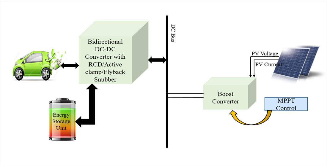
2 or other noxious gases when in use, they create a burden on the grid. Therefore, the coupling between the photovoltaics (PV) and charging stations for EVs is beneficial, as it allows greater usage of both EVs and solar energy without interrupting the grid’s capacity and provides better power quality. The solar-based charging station is primarily applicable on highways and remote locations to successfully charge EVs [1]. Kumar et al. [2] proposed a PV-based off-grid charging station in which the solar source is coupled with an energy storage unit (ESU) efficiently for variable irradiance conditions. The system enhances the reliability of the off-grid charging station for EVs. However, they used a non-isolated bidirectional converter with no capability of attaining zero-voltage switching (ZVS) characteristics. This is likely to result in a decrease in the overall efficiency of the charging station. Therefore, in this paper, we present a bidirectional DC–DC converter (BDC) with snubber circuits and demonstrate that a near ZVS across BDC switches is achieved for an off-grid charging station for EVs. This is expected to yield a higher efficiency PV-based charging station for EVs.
Since EVs are operated at low voltage levels, there is a need for an interface between the BDC and the charging station. Isolated BDC offers many advantages over non-isolated BDC: for example, bidirectional energy flow, electrical isolation, high reliability, etc. This BDC will be used for both stepping up and stepping down the voltage. Thus, charging and discharging can be combined in one circuit topology. Moreover, a full-bridge BDC is popular, due to its high power-handling capacity. However, the leakage inductance of the isolation transformer will result in high voltage and current spikes during switching transitions.
Additionally, the freewheeling current increases the conduction losses and reduce the effective duty cycle, due to the effect of leakage inductance. An alternative method is to charge the leakage inductance to the current level of the current-fed inductor, thereby reducing the current difference as well as reducing the voltage and current spikes. However, it is difficult to tune the switching diagram to match these two currents, as the current level varies with the load conditions [3].
The aforementioned problems can be overcome by using different types of snubber circuits. The snubber circuits provide an alternate path for the circulating current across BDC switches. The snubber is used to control the effect of the reactance of the circuit. It improves the switching circuit’s performance overall. The snubber absorbs the energy from the reactive elements in the circuit. As a result, the stress across the switch is reduced. This automatically increases the converter’s reliability [4,5]. Snubbers may be either passive or active networks. Passive snubbers are made of resistors, inductors, capacitors, or diodes, whereas active snubbers use transistors or other types of active switching elements. A conventional passive approach is to employ a resistive capacitive diode (RCD) snubber to clamp the voltage and the resistor limits the capacitor discharge current. The active clamped snubber used for BDC recycles the energy stored in the leakage inductance, thereby improving the converter efficiency. Another type of snubber is a flyback snubber in which the voltage spike across the switches gets clamped by a capacitor-diode circuit and is recovered. This snubber also provides an effective solution to reduce the circulating current across the BDC switches [6].
The implementation and benefits of snubber based BDCs in EVs were reported in the recent past [6,7]. However, there are negligible data on the use of snubber based BDCs for use in off-grid charging stations for EVs. Kumar et al. [2] described a standalone charging station, but this station does not use any snubber circuit. In the previous study [3], the beneficial effects of using a flyback snubber were reported. However, a systematic comparison of the performance of the off-grid EVs charging station with various available snubber circuit configurations was not performed. Hence, in this paper, RCD, active clamp, and flyback snubbers for the BDC in terms of the overall performance off-grid charging station for EVs are compared. Such a study was carried out on the BDCs in EVs which operate at low-voltage levels only [6,7]. However, there have been no reported results on either off-grid or grid-connected charging stations for EVs. In this paper, the proposed configuration of BDC with snubber circuits effectively reduces the impact of circulating current on the main switches, thereby effectively clamping the voltage spikes across the switches. This leads to an improved performance of the off-grid charging station for EVs. Furthermore, it is cheaper and cost-effective to have just one snubber circuit in the charging station instead of having one in each electric vehicle. Hence, a study of the performance of charging stations for EVs with various snubber circuit configurations is both meaningful and important.

2. Analyses of the Snubbers

The BDC used in [2] consists of a voltage source as a DC link capacitor and MOSFET switches for step-up and step-down modes. The load source is inductive, as the converter is a voltage source. When the switch’s state changes from turn-off or turn-on, the time lapse for transition can cause an overvoltage condition. Additionally, due to the reverse recovery of the free-wheeling diode, the switches show a current spike at turn-on, leading to high switching losses, especially at turn-off. These problems can be minimized/eliminated with the introduction of snubber circuits.
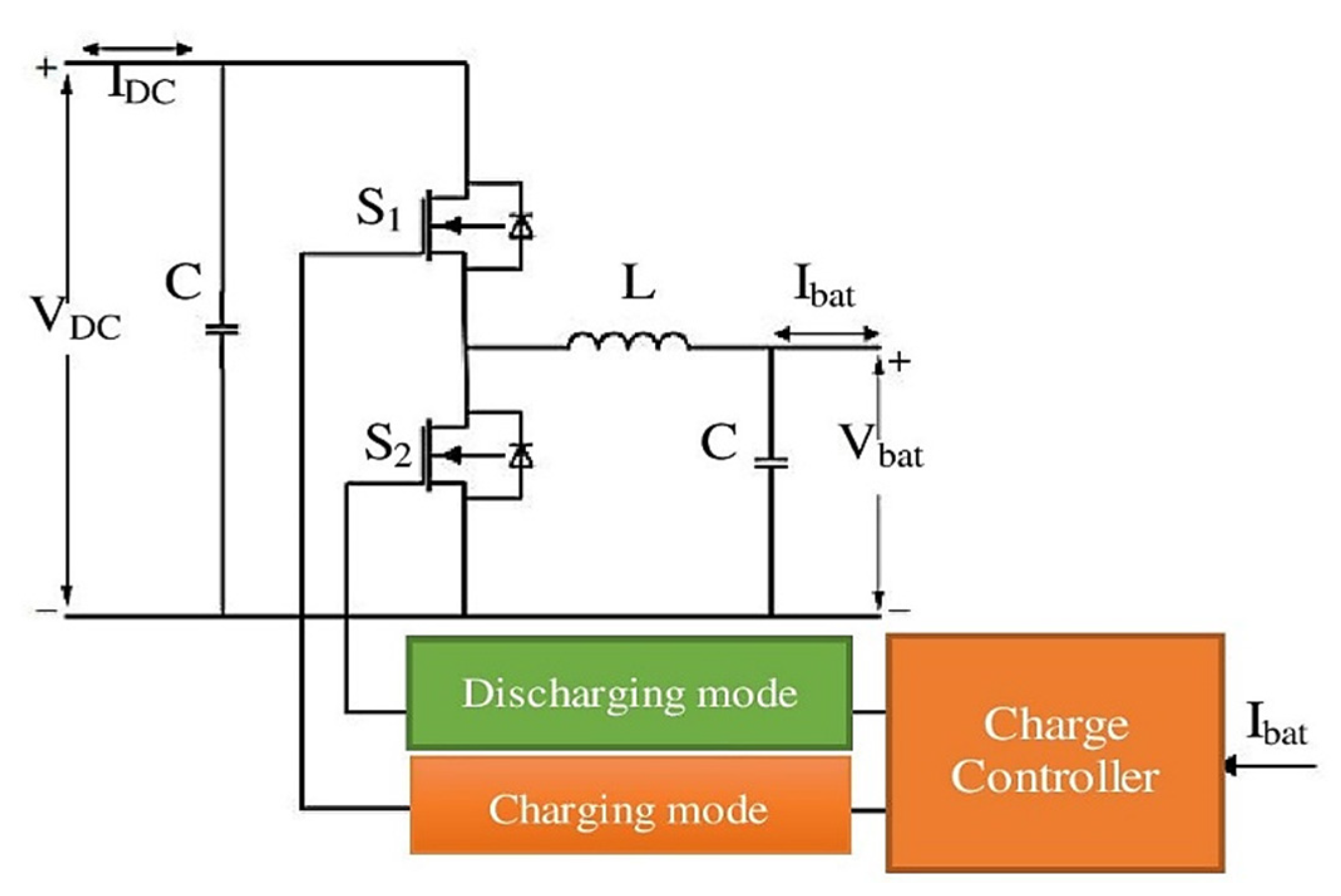
The proposed system [2] consists of a BDC model, which operates both in charging (buck) and discharging (boost) modes as shown in Figure 1. In the charging mode, DC-link acts as an input of BDC and the battery acts as a load on the output side. The battery’s voltage level is achieved at the output side when BDC operates in buck mode with component as an inductor (Lbuck). This value is calculated as follows:
L b u c k = [ | V D C V b a t | ( 1 D ) ] Δ i L f s
where ΔiL and fs are the ripple current switching frequency of the buck mode, respectively. VDC and Vbat are input and output voltages of the bidirectional converter, respectively, and D is the converter’s duty ratio.
In the discharging mode, the battery is connected as an input and DC-link connected as the output and the DC-link voltage is more than the battery terminal voltage. The component inductor (Lboost) in boost mode is calculated as follows:
L b o o s t = V b a t D Δ i L f s
Since the BDC is operating in both boost and buck modes, the value of L is chosen as follows:
L = max ( L b u c k ,   L b o o s t )
For comparison, the converters with an RCD passive snubber, an active clamping circuit, and a flyback snubber were simulated.
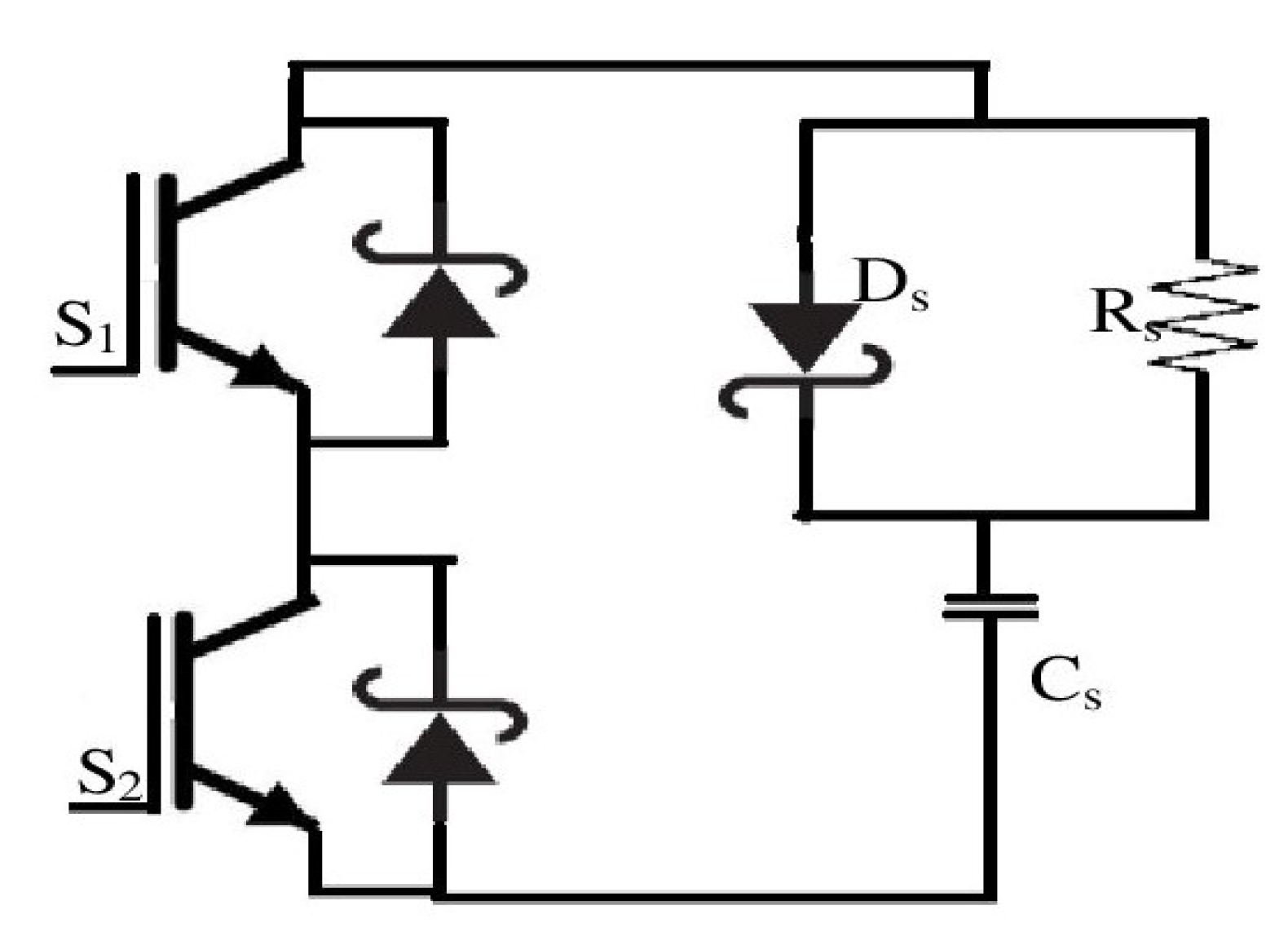
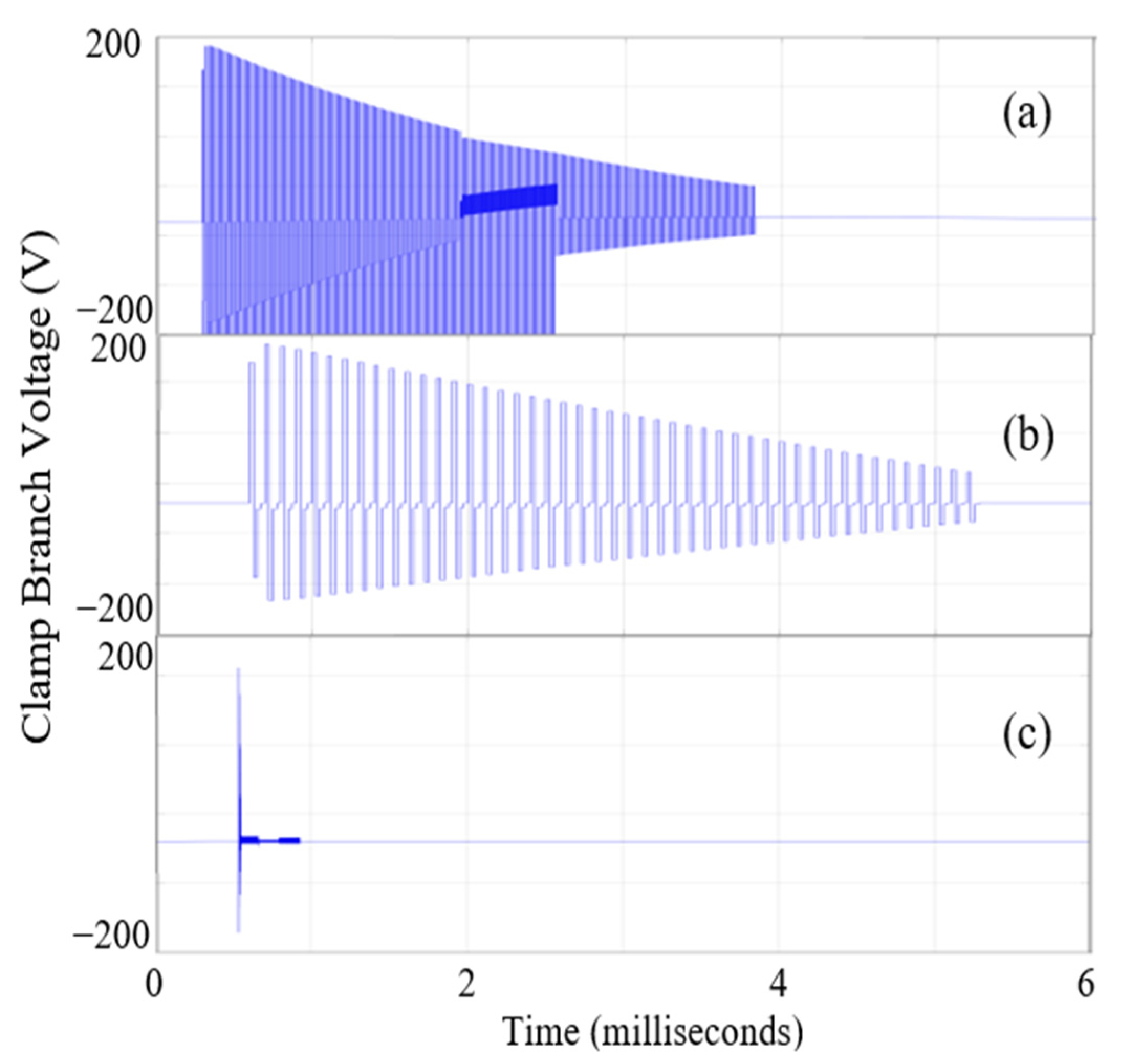
2.1. RCD Snubber

RCD snubber or RCD clamp limits any sharp voltage fluctuations across the switches. The three main components of RCD snubber are resistor Rs, the capacitance Cs, and diode Ds for as shown in Figure 2. The stored leakage energy is dissipated through the resistor while the capacitor acts as a filter to and guarantees a low ripple DC source. The diode here is nothing but a unidirectional switch. The clamping of the spikes using an RCD snubber requires calculating the resonant circuit’s characteristic impedance, given by the following equation:
Z = 2 π f s L
If the snubber resistor value is equal to the characteristic impedance, the ringing effect is reduced. Therefore, to select the resistor, the following equation is used:
R s = Z
The snubber capacitor, Cs, allows the resistor to be most effective at the ringing frequency by reducing the dissipation to a minimum at the switching frequency. The capacitor is designed so that the impedance of the capacitor at the clamping frequency is considered equal to the resistor, as shown in the following equation:
C s = 1 2 π f s R
where fs is the switching frequency of the converter.
The RCD snubber works by absorbing the inductor’s current when the switch’s drain voltage exceeds the clamp capacitor voltage. The relatively large capacitor used in the circuit manages to keep the voltage constant over a switching cycle. By using a larger capacitor value, the peak power will increase while the switching loss will decrease [8].

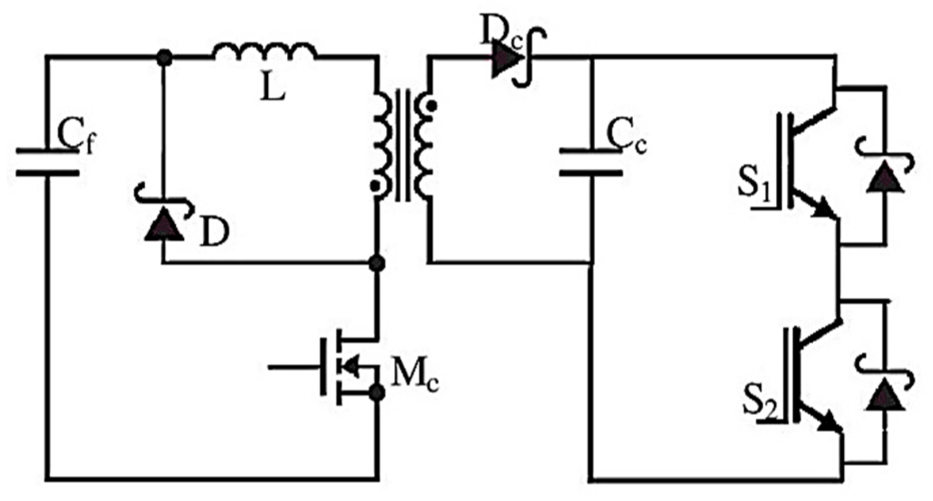
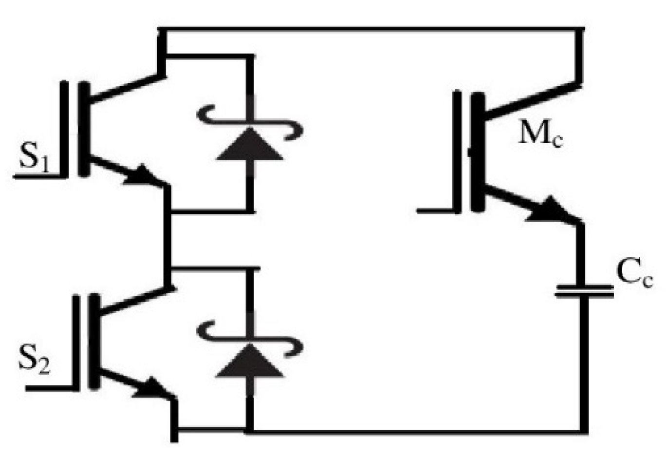
2.2. Active Clamp Snubber

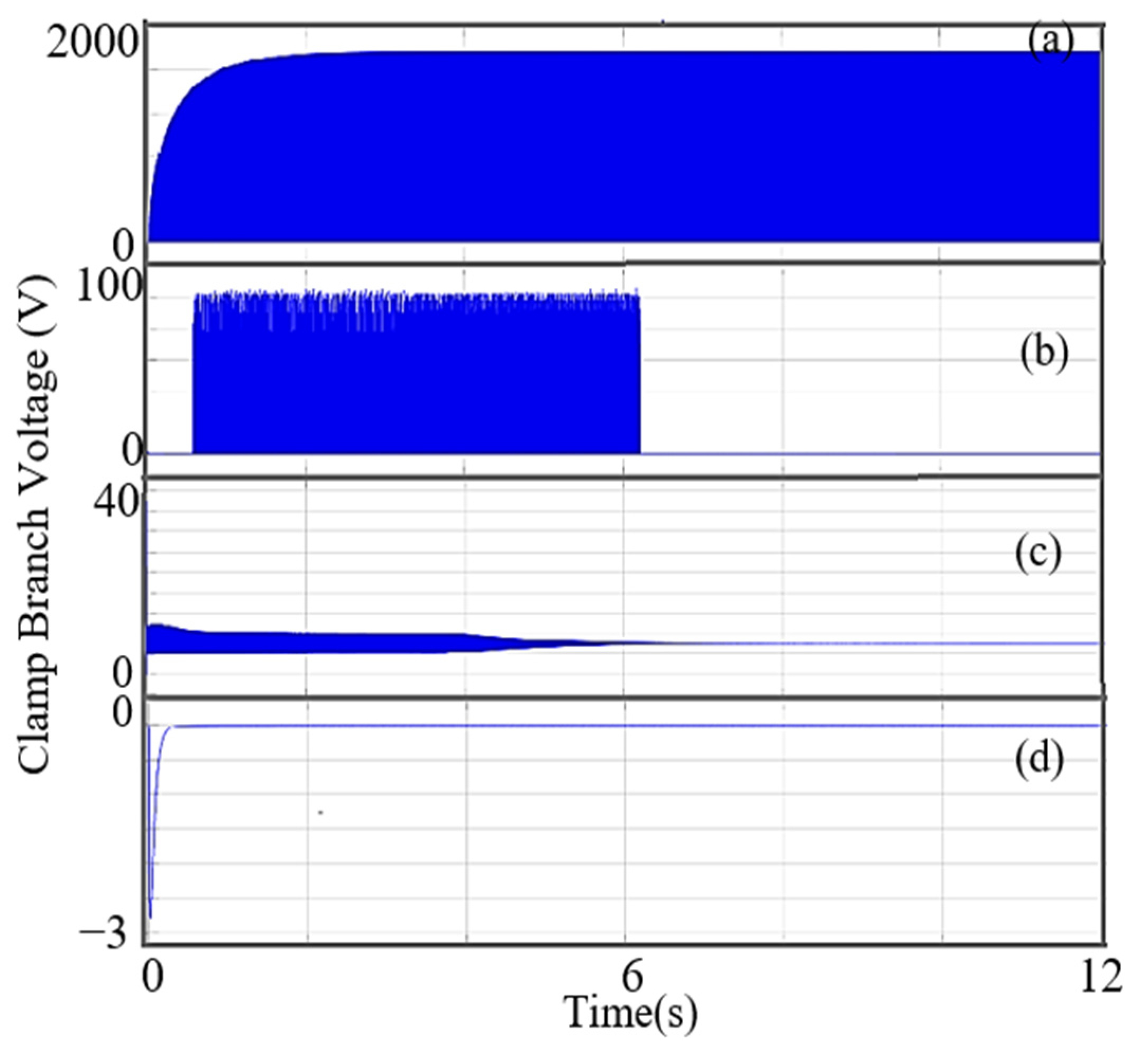
An active clamp for the BDC’s higher power applications is a good choice. It limits the overshoot of the bridge switch’s turn-off voltage, thus enabling the energy stored for ZVS. The output diode’s reverse-recovery problem can partly be overcome by utilizing an appropriate design for the leakage inductance. However, the switches in these converters work under hard switching conditions. The active clamp circuit replaces the role of the passive lossless clamp circuit. The primary and the clamp switches turn ON under the ZVS condition, and the use of parallel capacitors help significantly reduce the turn OFF losses.
As shown in Figure 3, the coupled inductor included in the topology is used to recycle the leakage inductance energy and achieve the ZVS condition for the main and clamp switches. The switches and diodes’ voltage stresses are lower than the output voltage. Thus, by using an active clamp circuit with an active switch Mc, and a capacitor, Cc,, conduction losses and cost can be significantly reduced.
The design is based on the resonant tank circuit formed by the clamping capacitor Cc and the leakage inductance Lk. Resonance occurs during the off-stage of the boost mode operation. The criterion to select Cc is such that the following holds:
C c   ( T s / 4 π ) 2 L k
where Ts is the period of the driving signal for each bridge switch of the converter [9,10].

2.3. Flyback Snubber

A flyback snubber is suitable for high power applications and is shown in Figure 4. This snubber circuit enables the main switch to achieve a ZVS turn-on or a ZCS turn-off process as a result of short time interval of ZVS or ZCS characteristics. The use of the series inductor results in slowing down the diode’s reverse recovery current. However, these inductors increase the switching loss, due to additional voltage stress on the main switch at turn-off transition. The snubber capacitor enables to clamp the switch voltage by absorbing the stored energy of the snubber inductor. However, the converter reliability and life span deteriorate as a result of the snubber capacitor’s energy reprocessing through the main switch, resulting in high current stress. The use of flyback snubber helps overcome this problem through its ability to attain soft-switching features and thus, significantly reduces both the voltage and current stresses. The flyback snubber can also achieve near ZVS and ZCS. It also significantly reduces any current and voltage stresses on the main switch. The output voltage ripple in flyback converter is given by the following:
Δ V 0 V 0 = D T s C f
where Cf is the capacitor of the flyback converter, and the output voltage ripple (ΔV0/V0) is considered to be 3%. Thus, the snubber capacitor for the flyback snubber can be calculated using Equation (8) [11,12].

3. Simulation Results

  • CASE 1 Using model proposed by Kumar et al. [2]
The system presented in [2] consists of a 24 kW PV generation for the 15 kWh battery (of EVs) coupled with an ESU of 15 kWh capacity. The ESU acts as a reserve for the batteries of EVs during times when PV generation is low and stores the energy during excess PV energy generation. Three modes for electrical vehicle battery charging were considered: (i) with PV energy only, (ii) with both PV energy and ESU energy, and (iii) with ESU energy only. The three modes are simulated using MATLAB/Simulink and the results are compared for each snubber circuit for the BDC in the charging station in the following sub-sections.

3.1. Charging Battery of EVs with PV Energy Only

In this mode, the PV generation is in abundance and is adequate to charge the battery of EVs (Figure 5). The DC-link voltage is maintained constant and supplies the required terminal voltage for the batteries continuously. Figure 6 shows the power variations in EVs, using three different snubber circuits with the BDC in this mode.

3.2. Charging Battery of EVs with PV Energy and ESU Energy

In this mode, the PV energy alone is insufficient to charge the EVs (Figure 7). Any additional energy is supplied by the ESU to charge the battery of EVs. Figure 8 shows the power variations of EVs when using three different snubber circuits with the BDC in this mode.

3.3. Charging Battery of EVs with ESU Only

In this mode, the battery of EVs is charged only from the ESU. The PV generation is almost zero. Figure 9 shows the power variations of EVs when using three different snubber circuits for the BDC in this mode.
The results presented in these three cases clearly show that this standalone charging station can charge the battery of EVs under any circumstance. It is an attractive way of using renewable energy. Figure 10 shows the clamp branch voltage across the main switches of the BDC.
It is evident from the graph that without a snubber circuit possessing higher voltage stress across the switch, it does not achieve the ZVS condition. In contrast, the three proposed snubber circuit attain ZVS condition rapidly. The RCD snubber circuit attains ZVS within six seconds. Using the active clamp snubber results in a significantly smaller voltage stress, and using the flyback snubber attains ZVS almost instantaneously. It is evident from the graph that the flyback snubber is the best option, as it can achieve ZVS by mitigating the voltage stresses. It is also clear from Figure 6, Figure 8 and Figure 9 that the power of EVs improves when snubber circuits are implemented. Additionally, the power waveforms clearly show that the use of the flyback snubber in the charging station results in the highest output power, compared to the other two snubber circuits.
  • CASE 2 Using Model proposed previously by the authors [3]
We used a standalone charging station for EVs [3]. It consists of a PV panel, ESU, BDC with a snubber circuit—the EVs act as the load. The system uses a PV panel with a capacity of 100 kWh. An ESU with a capacity of 80 kWh stores the power to charge 40 kWh EVs. The performance of the proposed charging station was carried out using MATLAB/Simulink by considering three cases—EVs are charged (i) with the PV array only, (ii) with both PV array and ESU, and (iii) with the ESU only [3]. Figure 11 shows the clamp branch voltage across each active snubber circuit. There is a power dissipation in the resistor of the RCD snubber. This means a reduced efficiency and is ideal for high-power operations. The burden of high current stress and associated thermal issues of the active switches and the capacitor limits the use of an active clamp snubber circuit in the BDC topology, as it switches at a frequency that is two times the switching frequency. From the voltage-clamp branch waveform, BDC using the RCD snubber and active clamp snubber causes more voltage transients. Meanwhile, the BDC with the flyback snubber can clamp the voltage better than all the other snubber circuits. Thus, transients can be avoided in the circuit. Figure 12 and Figure 13 show the output voltage obtained for the BDC using three different snubber circuits and the power of EVs. The BDC with the flyback snubber attains the steady state faster when compared to the other snubber circuits. Once again, the power waveforms clearly show that the use of the flyback snubber in the charging station results in the highest output power, compared to the other snubber circuits.
A comparative analysis between the various snubber circuits is shown in Table 1. From the table, it is clear that all three snubber topologies can be used successfully with the BDC for an off-grid charging station for EVs. Therefore, choosing the most suitable snubber circuit depends on voltage ripple, ability to achieve ZVS, and conduction losses. Thus, the flyback snubber provides the best option, compared to other snubber circuits while considering the aforementioned factors. However, the flyback snubber has the drawback of a complex structure, being more difficult to implement with the BDC, compared to other snubbers, and its cost is somewhat higher than the other snubber circuits. Nevertheless, one can ignore these disadvantages, as it offers superior performance with the BDC for the off-grid charging station, achieving ZVS, mitigating the voltage spikes and providing better efficiency than the other snubber circuits.
These scenarios clearly demonstrate that a stand-alone PV-based charging station is equipped to successfully charge EVs under any condition. The snubber circuit in the BDC results in a system free from any high voltage stresses, which is energy efficient. The proposed isolated BDC with flyback and passive snubbers offers a viable solution to significantly reduce any circulating current issues and voltage spikes. Using a BDC with no snubber circuit will always suffer from voltage spikes, due to the presence of the inductor. The flyback snubber successfully reduces this voltage spike. Additionally, the flyback snubber, in addition to exhibiting excellent reliability and efficiency, can be controlled to attain a soft start-up feature. Figure 14 shows the plot of the efficiency curve, while maintaining a constant input voltage for the two case studies described in this paper. This curve was obtained with a fixed input voltage of 400 V. The maximum efficiency for case 1, having BDC with flyback snubber and passive snubber, is 90%, whereas for case 2, it is about 92%. It was previously shown in [3] that the efficiency of BDC without the snubber circuit was less than the BDC with a snubber circuit. The efficiency curves shown in Figure 14 indicate that an off-grid charging station for EVs by using a BDC with snubber circuits is improved.

4. Conclusions

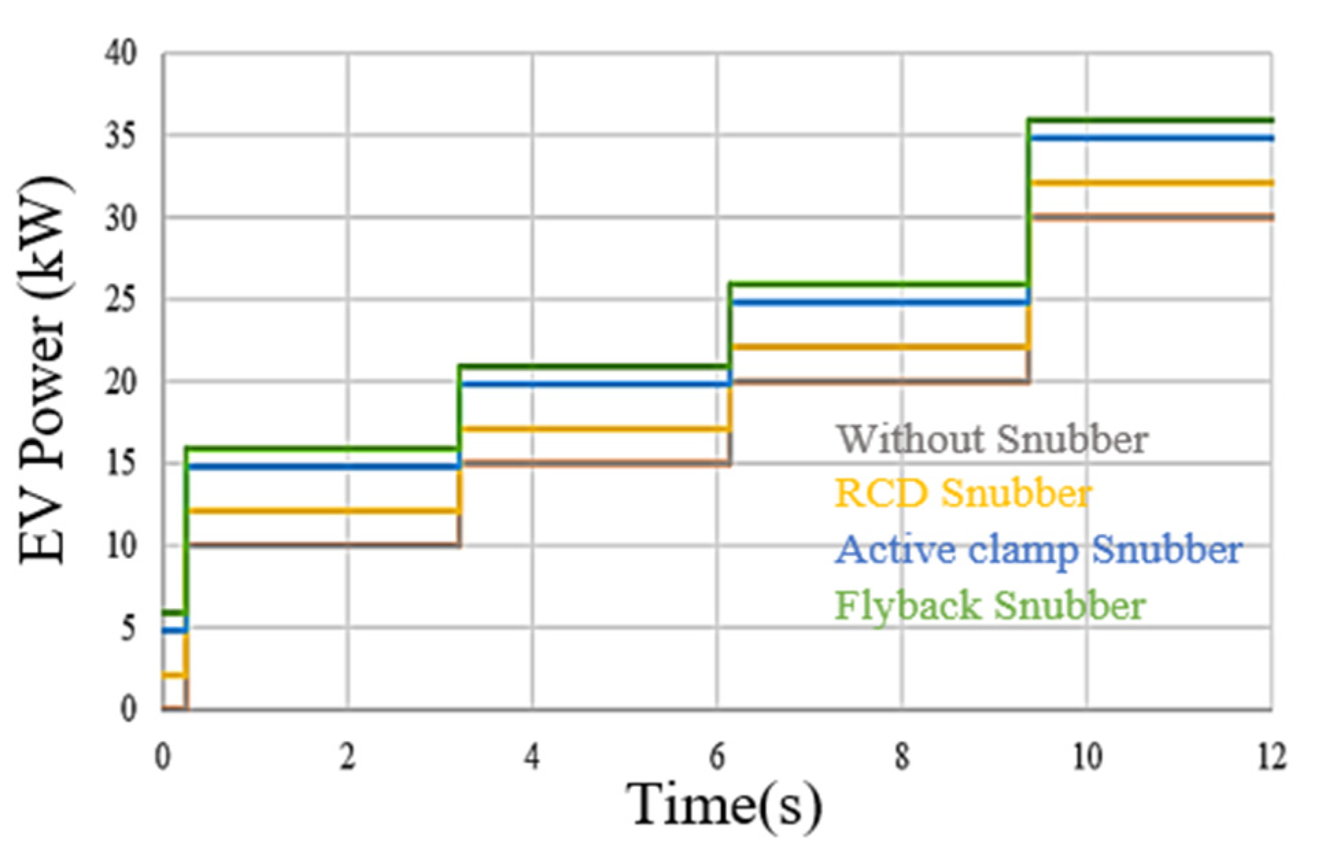
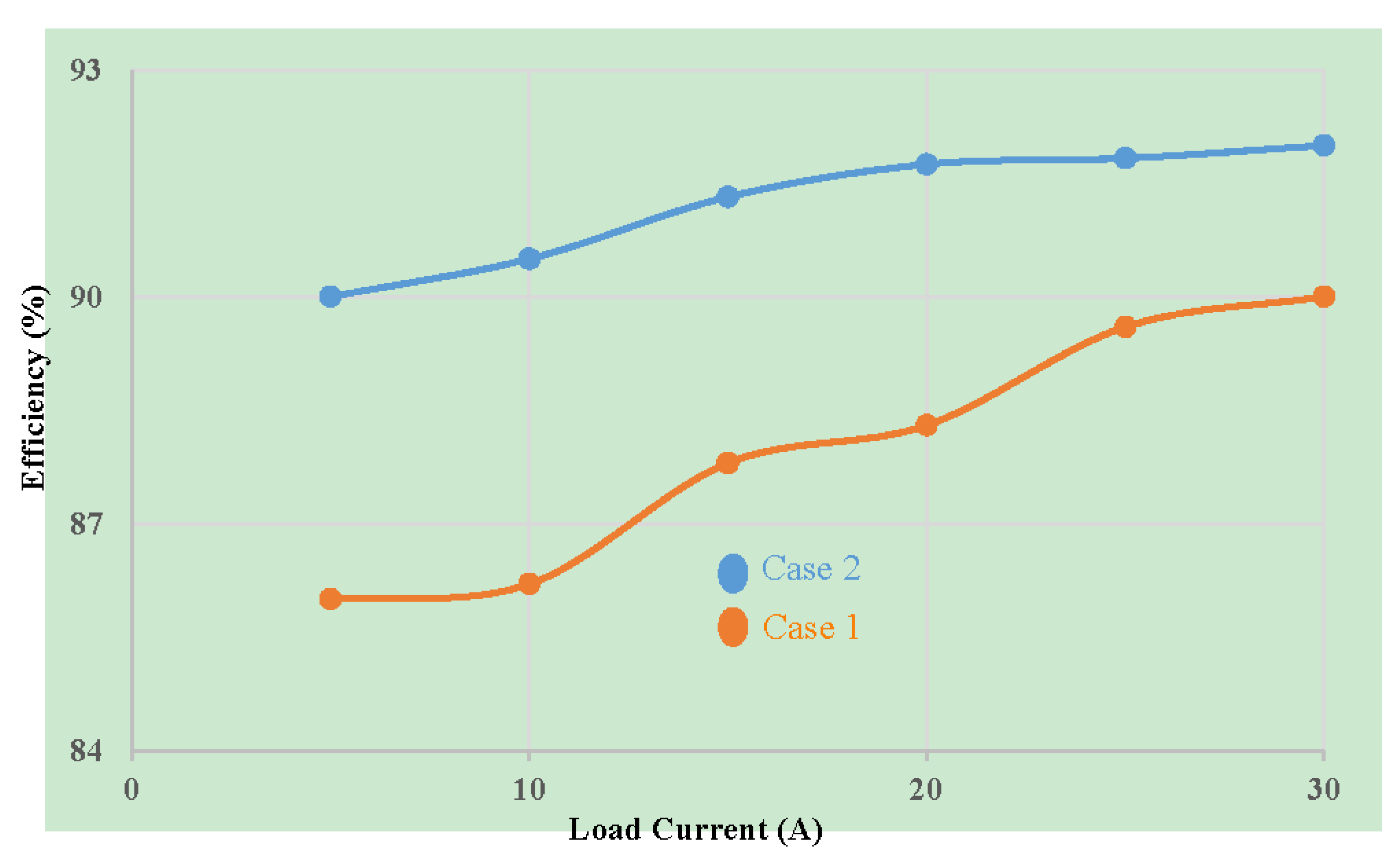
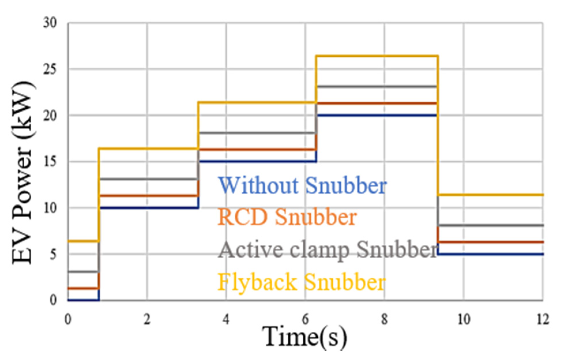
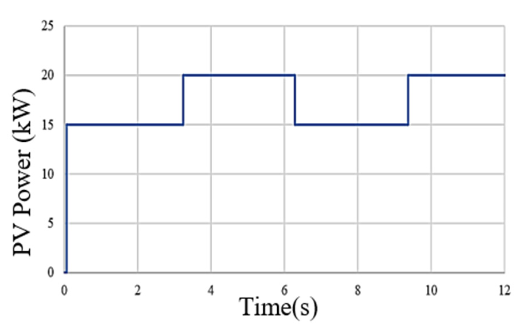
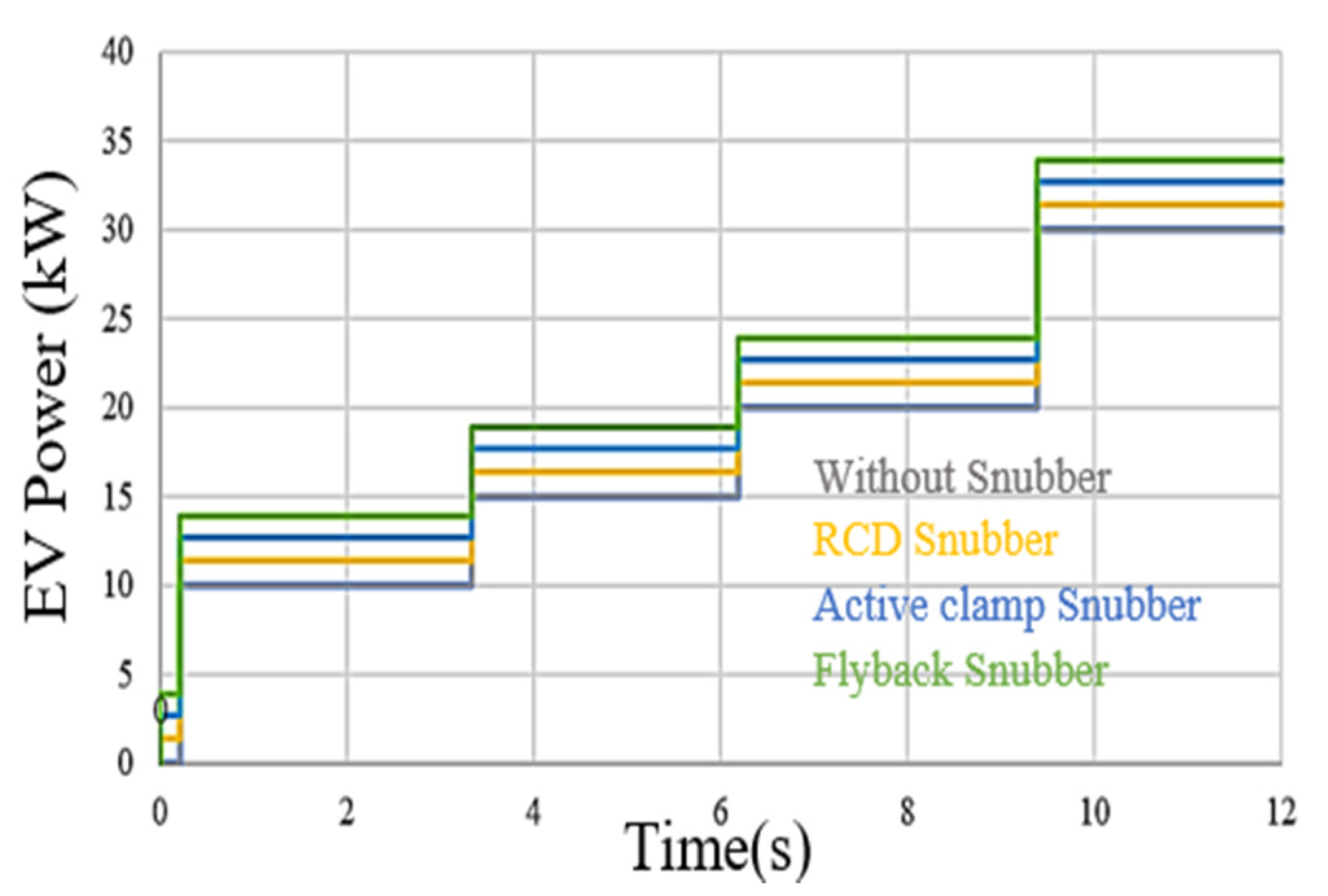
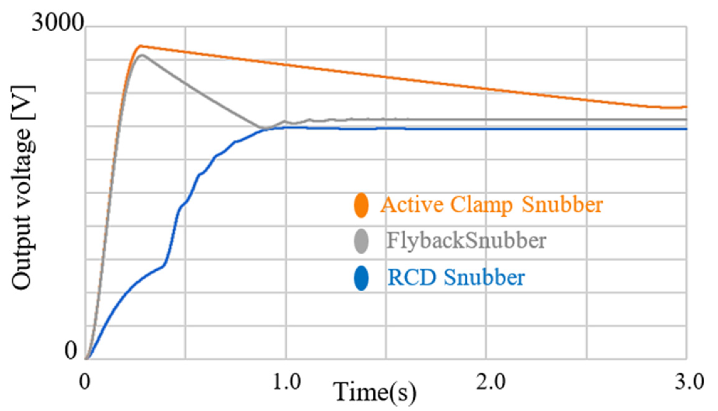
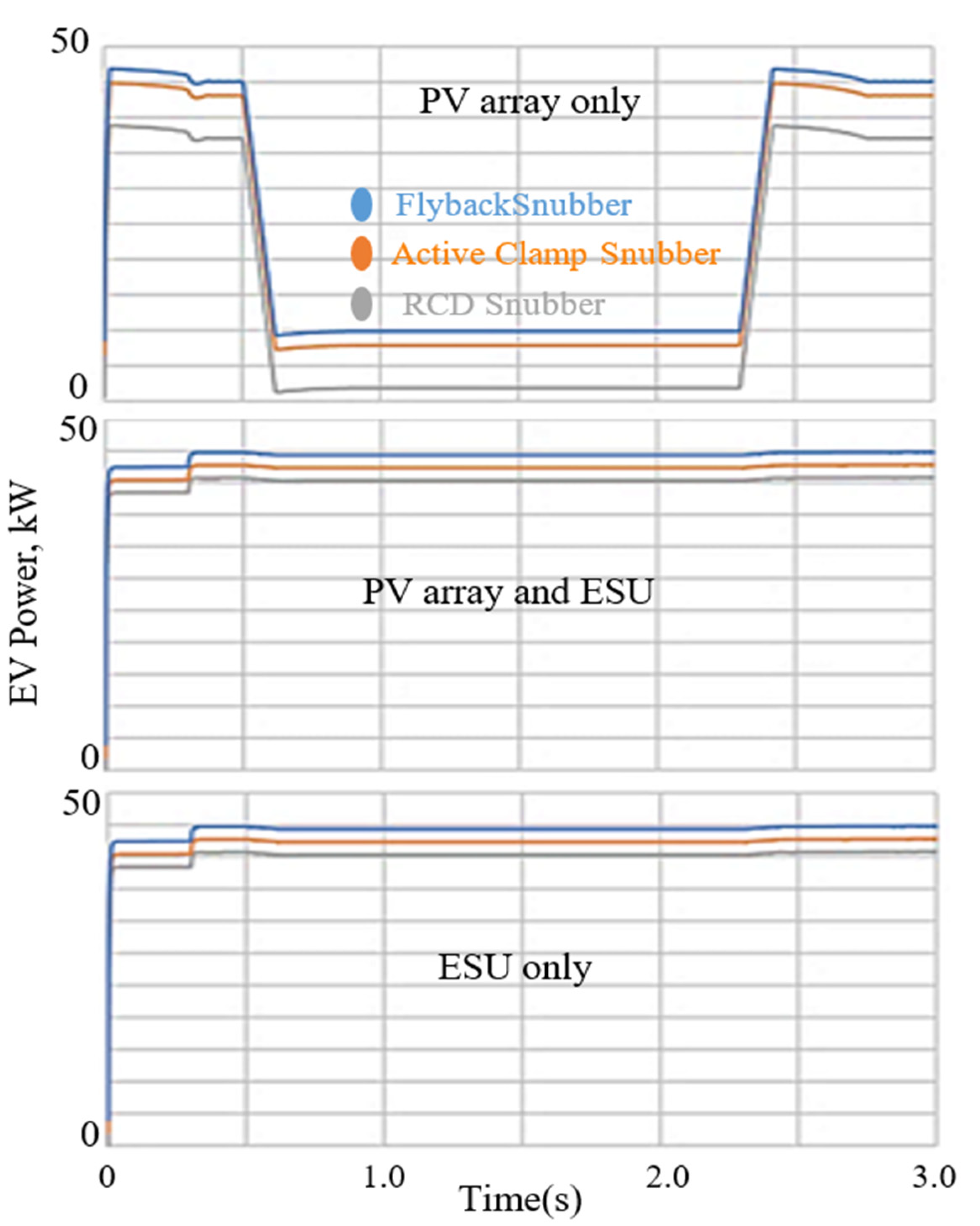
In this paper, various snubber circuits for the BDC of two different models of an off-grid solar-based charging station for EVs were implemented and studied. A performance comparison of the charging station was carried out. The use of PV to charge EVs in an off-grid charging station will help to achieve clean energy generation and reduce the grid burden. Thus, the use of EVs in remote locations can be significantly increased. An ESU is coupled with the system to work under any circumstances. The proposed BDC incorporates either RCD snubber or active clamp snubber or flyback snubber to reduce the voltage spike caused by the current fed inductor. The proposed station’s design using various snubber circuits was explained and validated in MATLAB/Simulink. It was successfully tested on two independent models, thus making the method both credible and robust. The efficiency of the proposed converter with the snubber circuits in both the cases is higher, compared to the converter without snubbers. The converter can achieve ZVS conditions more rapidly than a converter without the snubber. Thus, the use of an appropriate snubber enhances the system reliability efficiency. In both the models reported here, the flyback snubber consistently offered the best possible results.

Author Contributions

Conceptualization, D.K.N. and K.P.; methodology, D.K.N.; software, D.K.N.; validation, D.K.N., K.P. and T.T.L.; formal analysis, D.K.N.; investigation, D.K.N.; resources, D.K.N.; data curation, D.K.N.; writing—original draft preparation, D.K.N.; writing—review and editing, D.K.N. and K.P.; visualization, D.K.N.; supervision, K.P. and T.T.L.; project administration, K.P. and T.T.L. All authors have read and agreed to the published version of the manuscript.

Funding

This research received no external funding.

Conflicts of Interest

The authors declare no conflict of interest.

References

  1. Shariff, S.M.; Alam, M.S.; Ahmad, F.; Rafat, Y.; Asghar, M.S.J.; Khan, S. System Design and Realization of a Solar-Powered Electric Vehicle Charging Station. IEEE Syst. J. 2020, 14, 2748–2758. [Google Scholar] [CrossRef]
  2. Kumar, V.; Teja, V.R.; Singh, M.; Mishra, S. PV Based Off-Grid Charging Station for Electric Vehicle. IFAC-PapersOnLine 2019, 52, 276–281. [Google Scholar] [CrossRef]
  3. Nair, D.K.; Prasad, K.; Lie, T.T. Standalone electric vehicle charging station using an isolated bidirectional converter with snubber. Energy Storage 2021, e255. [Google Scholar] [CrossRef]
  4. Sharon, P.; Sathiyan, P.S. Design and simulation of bidirectional converter with flyback and capacitor diode snubbers. In Proceedings of the 2015 International Conference on Innovations in Information, Embedded and Communication Systems (ICIIECS), Coimbatore, India, 19–20 March 2015; pp. 1–5. [Google Scholar]
  5. Todd, P.C. Snubber Theory, Design Circuits and Application. Available online: https://www.ee.bgu.ac.il/~dcdc/notes/Additional_2012/Snubbers.pdf (accessed on 13 September 2021).
  6. Bhatt, K.; Gupta, R.A.; Gupta, N. Design and development of isolated snubber based bidirectional DC–DC converter for electric vehicle applications. IET Power Electron. 2019, 12, 3378–3388. [Google Scholar] [CrossRef]
  7. Wu, T.-F.; Chen, Y.-C.; Yang, J.-G.; Kuo, C.-L. Isolated Bidirectional Full-Bridge DC–DC Converter With a Flyback Snubber. IEEE Trans. Power Electron. 2010, 25, 1915–1922. [Google Scholar] [CrossRef]
  8. Vaz, A.R.; Tofoli, F.L. In-depth analysis of an RCD snubber applied to a DC-DC boost converter. Int. J. Circuit Theory Appl. 2021, 49, 283–305. [Google Scholar] [CrossRef]
  9. Yoo, J.S.; Ahn, T.; Yu, G.; Lee, J.; Lee, J. A study on novel active clamp snubber applied DC-DC quasi resonant flyback converter to effectively reduce switch voltage surge. In Proceedings of the 2017 20th International Conference on Electrical Machines and Systems (ICEMS), Sydney, Australia, 11–14 August 2017; pp. 1–5. [Google Scholar] [CrossRef]
  10. Yan, Z.; Zeng, J.; Liu, J.; Lin, W. A Novel Soft-Switching Bidirectional DC-DC Converter with High Voltage-Gain for Grid-Connected Energy Storage System. In Proceedings of the 2019 4th IEEE Workshop on the Electronic Grid (eGRID), Xiamen, China, 11–14 November 2019; pp. 1–6. [Google Scholar] [CrossRef]
  11. Balbayev, G.; Nussibaliyeva, A.; Tultaev, B.; Dzhunusbekov, E.; Yestemessova, G.; Yelemanova, A. A novel regenerative snubber circuit for flyback topology converters. J. Vibroengineering 2020, 22, 983–992. [Google Scholar] [CrossRef]
  12. Tadvin, S.M.; Bin Shah, S.R.; Hossain, M.R.T. A Brief Review of Snubber Circuits for Flyback Converter. In Proceedings of the 2018 3rd International Conference for Convergence in Technology (I2CT), Pune, India, 6–7 April 2018; pp. 1–5. [Google Scholar] [CrossRef]
Figure 1. Circuit diagram of the bidirectional converter [2].
Energies 14 05853 g001
Figure 2. Circuit diagram of the RCD snubber [8].
Energies 14 05853 g002
Figure 3. Circuit diagram of the active clamp snubber [9,10].
Energies 14 05853 g003
Figure 4. Circuit diagram of the flyback snubber [11,12].
Energies 14 05853 g004
Figure 5. Power response curve of PV.
Energies 14 05853 g005
Figure 6. Power response curve of EVs.
Energies 14 05853 g006
Figure 7. Power response curve of PV.
Energies 14 05853 g007
Figure 8. Power response curve of EVs.
Energies 14 05853 g008
Figure 9. Power response curve of EVs.
Energies 14 05853 g009
Figure 10. Clamp branch voltage of BDC (a) without snubber (b) RCD Snubber (c) active clamp snubber (d) flyback snubber.
Energies 14 05853 g010
Figure 11. Clamp branch voltage of BDC (a) RCD Snubber (b) active clamp snubber (c) flyback snubber.
Energies 14 05853 g011
Figure 12. Output voltage of bidirectional converter, using three different snubber circuits.
Energies 14 05853 g012
Figure 13. Output voltage of EVs load, using three different snubber circuits.
Energies 14 05853 g013
Figure 14. Plot of conversion efficiency of the proposed converter.
Energies 14 05853 g014
Table 1. Comparative analysis of various snubber circuits.
ParametersRCD SnubberActive CLAMPING SNUBBERFlyback Snubber
Number of switches/diodes/capacitors0/1/11/0/11/1/2
Conduction lossModerateLowVery low
Voltage rippleModerateLowNegligible
Attaining speed of ZVSVery slowSlowFast
Ease of implementation in BDCMuch easierEasyDifficult
ComplexitySmoothBit complexComplex
CostInexpensiveReasonableBit expensive
EfficiencyLowModerateHigh
Publisher’s Note: MDPI stays neutral with regard to jurisdictional claims in published maps and institutional affiliations.

