Article

DCM Boost PFC for High Brightness LED Driver Applications

1
Department of Physical Electronics, School of Electrical Engineering, Faculty of Engineering, Tel-Aviv University, P.O. Box 39040, Tel Aviv-Yafo 69978, Israel
2
Department of Electrical Engineering, Faculty of Engineering, Holon Institute of Technology, 52 Golomb St., Holon 5810201, Israel
*
Author to whom correspondence should be addressed.
Energies 2021, 14(17), 5486; https://doi.org/10.3390/en14175486
Submission received: 9 July 2021 / Revised: 19 August 2021 / Accepted: 25 August 2021 / Published: 2 September 2021

Abstract

:
This paper is concerned with the derivation of a discontinuous conduction mode boost PFC rectifier as a driver for high-power LED lighting applications. The proposed driver is operated in the current mode regime while emulating a resistance towards the line, thus attaining a near unity power factor and low total harmonic distortion of the line current. Theoretical analysis is reported and conditions for the low LED flicker are derived. A method of design for minimum THD is also suggested. Simulation and experimental results are reported.

1. Introduction

The next generation of lighting systems is hinged on high-brightness light-emitting diodes (LEDs). The high brightness LED is comprised of an array of rather small-sized basic LED devices put together to produce a significant amount of luminous flux for illumination purposes. The LED light source usually relies on high-energy blue LEDs covered by a phosphorus coating. The phosphorous coating converts the light spectra, that is, absorbs the blue light and emits a warm white light pleasant to the human eye. LEDs are very efficient, durable, maintenance-free, and have a long service life. Therefore, in the foreseeable future, LEDs are expected to replace much of the old incandescent and fluorescent light sources. By 2027, the widespread use of LED lighting in the US alone could save about 348 TWh—a total savings of more than $30 billion in today’s electricity prices [1,2].
LEDs are direct current devices that require a suitable and reliable AC/DC converter, aka LED driver, to connect to the grid. The expected popularity of LED lighting also implies that their prospective drivers are about to be manufactured and applied in great numbers. To prevent massive utility pollution, the emerging off-line LED drivers must comply with the existing harmonic regulations [1,2]. Therefore, the LED drivers of any significant power are expected to perform high-quality rectification, also referred to as power factor correction (PFC). At the output, due to their steep current–voltage characteristics, LEDs should be energized by a current source, whereas the input is a voltage source, which calls for driver circuits with gyrator characteristics [3,4,5,6].
In the past, power factor correction (PFC) rectifiers’ technology was intensely developed for industry, consumer, and military markets, and nowadays has reached maturity. The boost converter is frequently used in single-phase PFC applications due to its simplicity, robustness, high efficiency, and low part count [7]. At a higher power (>250 W), continuous current mode (CCM) operation is preferred due to its low-ripple input current that is easier to filter, whereas at the low power level (~100 W), the boost converter is usually operated in discontinuous conduction mode (DCM) with the advantage of attaining natural zero-current turn-off, and so alleviating the reverse recovery problems of the boost diode. Operation at a constant switching frequency also makes the EMI filter design easier [3]. However, unlike the popular DCM flyback PFC, which can provide a near unity power factor just by operating at a constant duty cycle [8,9], the DCM boost PFC rectifier tends to generate a much higher total harmonic distortion (THD) [10,11]. Therefore, to attain an acceptable THD performance, the DCM boost PFC requires a feedback control scheme to actively shape the line current.
Several control methods of boost PFC can be found in the literature [12]. The constant frequency peak current mode (PCM) [13] and the average current mode (ACM) controllers [14] are, perhaps, the most popular. These methods require the application of both an inner feedback loop to shape the line current (which includes current reference and error amplifier circuits) and an outer loop to regulate the output voltage. Thus, a substantial design effort is needed to attain proper compensator design. Two related approaches that offer simplified controller implementation of the boost rectifier belong to a class of “PFC with no input voltage sensing”. These are the non-linear carrier (NLC) [15,16] and the one cycle control (OCC) [17,18,19] techniques. Both methods can provide inherent line current shaping. Therefore, only the outer loop needs the designer’s attention.
The application of OCC to power factor correction is advantageous. The OCC controller for the CCM boost rectifier is simpler when compared with the traditional approach and can be easily implemented. Furthermore, OCC has the advantages of inherent stability and robustness. The ACM and OCC control methods for a bridgeless boost PFC were investigated by [20], who confirmed the superiority of the OCC approach. However, at light loading or near zero-crossing of the line voltage, the PFC stage usually undergoes CCM to DCM mode changes. This necessitates control law adjustments to avoid distortion in the input current. Improved boost PFC analog OCC controllers that can regulate the switch turn-on time or frequency according to the AC input line voltage and reduce the distortion in the vicinity of the line voltage zero-crossing have been suggested [21]. A Digital version of [21] was suggested in [18]. To overcome the CCM–DCM transition problem, [22] suggested increasing the switching frequency at the dips of the line, whereas a control strategy for bidirectional boost rectifiers based on the OCC of charge was proposed in [23]. A discrete-time OCC PWM modulator, implemented in FPGA, was proposed to a single-phase PFC boost converter by [24]. Digital systems are flexible and can implement complex control strategies. However, when PFC enters DCM, the limited numeric resolution and, consequently, duty cycle errors of the digital controller appear as additional sources of instability. The problem of mode transition was resolved in [25] by though a mixed conduction mode (MCM) digital controller with a DCM detection technique to realize boost PFC operating in both CCM and DCM during AC line half-cycle, and resulted in an improved THD performance. Yet, the above solutions for the mode transition problem complicate the OCC controllers and so diminish its key advantage.
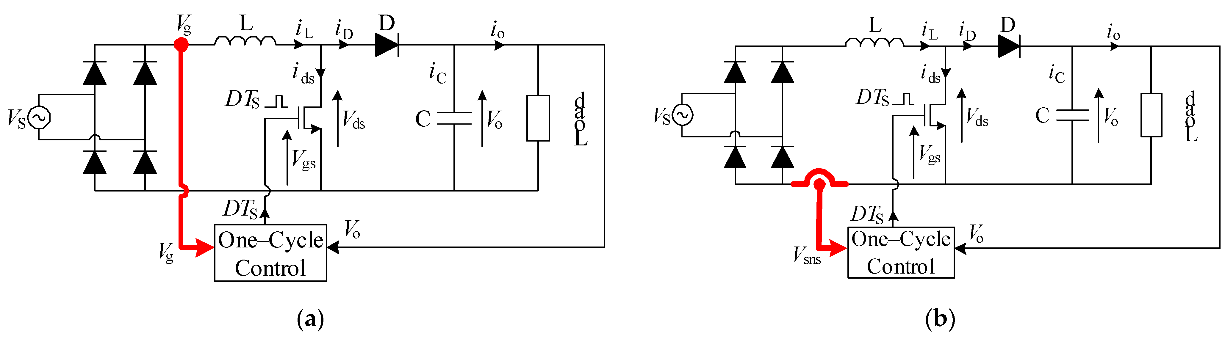
A straightforward solution to the problem of mode changes is designing the power stage to operate exclusively in DCM. Thus, no mode changes can be expected and the same control law can be effectively employed throughout the entire line cycle. An earlier OCC-controlled DCM boost PFC rectifier [19] relied on sensing both the rectified input and the output voltages to generate the required duty cycle (see Figure 1a). However, the analysis revealed that the OCC modulator in Figure 1a has the disadvantage of having the output power, P o u t , reciprocal to the modulation voltage, V m : P o u t = k / V m , where k is a system’s constant [19]. As a result, the increment of the PFC’s average output current, i ^ D , as function of the small signal variation of the modulation voltage, v ^ m , strongly depends on its power level: i ^ D = P o u t 2 k V o v ^ m . The non-linear and negative small signal loop-gain poses design difficulties and operational limitations, and, therefore, is a hindrance.
The rest of the paper is organized as follows. Section 2 presents a review of the basic quantities of the DCM boost power stage that are used in the next sections. Section 3 is concerned with the derivation of an alternative OCC control scheme for the DCM boost PFC rectifier with the aim of improving its dynamic characteristics. Unlike the earlier voltage feed-forward DCM OCC approach in Figure 1a, the proposed OCC controller in Figure 1b relies on sensing the inductor current to generate the duty cycle for the DCM boost PFC power stage. Thus, the proposed scheme is referred to as the current mode DCM OCC. In the past, the current mode OCC modulator was successively employed to control the CCM PFC rectifiers [17]; however, the CCM OCC control law is incompatible with the DCM operation. Therefore, in this paper, the current mode OCC is further investigated to formulate the required control law that suits the DCM boost PFC in Figure 1b. This is indeed derived and its key features are studied. The proposed controller has the advantage of having a linear relationship between the power and the control voltage, P o u t = k v m . As a result, the small signal gain is also linear and of a positive sign. This greatly alleviates the outer feedback loop design. Section 4 of the paper describes the static design considerations to help choose the storage capacitor to limit the light flicker to an acceptable level. Section 5 of the paper presents the small-signal model of the outer current loop and reports on the analytical results. In Section 6, a design example is given demonstrating the design of the OCC DCM boost PFC/LED driver to provide the preferred operational conditions for the LED string load. Lastly, in Section 7 and Section 8, the simulation and experimental results are reported.

2. Review of the Basic Relationships of DCM Boost PFC

To introduce the nomenclature and facilitate the analysis approach, the basic relationship of DCM boost PFC are reviewed first.
The topology of the boost PFC rectifier/LED driver is shown in Figure 2a. The peak inductor current, Ip, of the boost converter operating in the DCM mode, see Figure 2b, is given by
I p = 1 L V s d T s = 1 L ( V o V s ) d 1 T s
here, L is the boost inductor, Ts = 1/fs is the switching period, fs is the switching frequency, Vs is the source voltage, Vo is the output voltage, d is the on (switch) duty cycle, and d1 is the off (diode) duty cycle.
The ratio of the switch to diode duty cycle can be obtained from (1) as a function of the source and output voltages
d 1 d = V s V o V s
Then, applying geometrical considerations and using (1) and (2), the average inductor current can be expressed as
i a v = 1 T s [ 1 2 I p ( d + d 1 ) T s ] = 1 2 I p d ( V o V o V s ) = 1 2 V s L f s d 2 ( V o V o V s )
The above relationship will be useful in the following derivation of the DCM OCC control law.

3. The Proposed Line Current Shaping Method

3.1. Derivation of the Current Mode DCM Boost OCC Control Law

The control objective of the PFC is shaping the average current, iav, proportionally to the source voltage Vs, so that
i a v = V s R e
here, Re is the emulated resistance presented by the PFC towards the line, which can be evaluated in terms of the RMS source voltage, VRMS, and the average power, Pav, drawn throughout the line cycle
R e = V r m s 2 P a v
Combining (3), (4) and (3) leads to
i a v = V s R e = 1 2 V s L f s d 2 ( V o V o V s )
Rearranging (6) and applying (4) results in
V o R e i a v = 1 2 V o L f s d 2
The sensed voltage, vsns, at the output of the input current sensing network (see Figure 2a) is defined as
v s n s = i a v R s n s
here, Rsns is the low-frequency trans-resistance gain of the input current sensing network.
Furthermore, defining the modulation voltage, Vm, as
V m = V 0 R s n s R e = V 0 R s n s P a v V R M S 2
and the sensed output voltage, Vd, as
V d = R s n s 2 L f s V o
and applying the definitions (8–10) to (7) yields the current mode OCC control law of the DCM boost PFC
V m v s n s = V d d 2
The control law (11) can be realized by applying double integration as follows
V m v s n s = 2 T s 2 0 d T s ( 0 t V d d τ ) d t
This can be implemented in the hardware, as shown in Figure 2c.
With the proposed OCC controller, the DCM boost rectifier can attain the desired resistive input characteristic (4).

3.2. The Emulated Resistance

Further examination of (9) reveals that the average power is given by
P a v = 1 R s n s V R M S 2 V o V m
Note that the average power is linear with the modulation signal Vm. Thus, the latter can be used in control purposes to regulate (modulate) the load power. Note again that the advantage of the proposed approach stems from the above linear relationship.
Further substituting (13) into (5) yields the emulated resistance, Re, as a function of the modulation voltage, Vm, and the output voltage, Vo
R e = R s n s V o V m
The emulated resistance, Re, is a function of the current sensor gain, Rsns, but also depends on the ratio between the output voltage, Vo, and the modulation voltage, Vm.

4. Static Design of DCM Boost PFC/LED Driver

Static design of a boost converter involves properly choosing the values of the inductor, L, and the capacitor, C, of the power stage. Inductor design is well documented in the literature; however, in the case of LED driver application, selecting the capacitor value requires deeper consideration, as described below.

4.1. Output Ripple of a PFC with LED-String Load

Assuming the control circuit attains its goal of unity PF so that its average line current is a pure sinusoid, and considering the AC-DC power balance, the average diode current, supplied to the output filter and the LED load is
i D ( t ) = I o d c ( 1 C o s ( 2 ω L t ) )
Here ω L is the line’s angular frequency.
The LED string can be modeled by its Thevenin equivalent circuit. The simplified model is shown in Figure 3a. Here, Vth and rth are the Thevenin equivalent voltage and Thevenin equivalent resistance of the LED string respectively. According to Figure 3a, the LED current, io, is simply
i o = 1 r t h ( v o V t h )
Applying KCL to the output node, i D ( t ) = i C + i o , and using, i c = C d v o d t , yields the differential equation for the output voltage
C d v o d t + v o V t h r t h = I o d c ( 1 C o s ( 2 ω L t ) )
whence the output voltage is derived as
v o ( t ) = V t h + r t h I o d c ( 1 1 1 + C n 2 cos ( 2 ω L t α ) )
Here, the normalized output capacitor is defined as C n = C / C b , the base capacitance is defined as C b = 1 2 ω L r t h and the phase shift is α = tan 1 ( C n ) , see Figure 3b. Using (16) and (18) the LED string current can be obtained as
i o ( t ) = I o d c ( 1 γ C o s ( 2 ω L t α ) )
where the peak LED string current ripple is defined as
γ = I o p k I o d c = 1 1 + C n 2
The LED string current is illustrated in Figure 3b as having an average value of Iodc with a superimposed second harmonic ripple component of amplitude Iopk. The unwanted second harmonic current causes LED flickering.
Figure 4 presents a plot of the LED current ripple, γ , as a function of the normalized output capacitor C n . Equation (19) predicts that the LED current ripple, γ , is constant depending on the system parameters. This also means that the LED flicker is constant. The flicker is also independent of the power level, which is an advantage. The flicker can be reduced by a proper choice of the filter capacitor, C, given by
C n = C C b = ( 1 γ ) 2 1

4.2. Flicker Considerations

According to [26], the percent of flicker is defined as follows:
M o d % = 100 M a x M i n M a x + M i n
where Max and Min are the levels of the LED’s light intensity over a single period of the LED current.
As the LED light intensity is proportional to the LED current, the modulation is
M o d % = 100 ( I o d c + I o p k   ) ( I o d c I o p k   ) ( I o d c + I o p k   ) + ( I o d c I o p k   ) = 100 I o p k I o d c = 100 γ
Reportedly, flickering light can adversely affect human wellbeing. The percent of a flicker threshold level for no noticeable harm, where the flicker might only cause discomfort to some people but photosensitive seizures would not occur, is
M o d % 0.08 f F l i c k e r
where f F l i c k e r is the flicker frequency, which is the frequency that corresponds to the periodic change in the light intensity level [26].
The flicker of a single-phase LED driver is due to the output ripple, which is at the second harmonic of the line frequency f F l i c k e r = 2 f L , where fL is the line frequency. From (23), (24) complies with the “no noticeable harm” condition and the allowable ripple at the output of the LED driver has to be restricted to
γ 0.08 100 f F l i c k e r
Applying (25) and (20) to (24), the “no noticeable harm” criteria for C n can be formulated as follows:
C n ( 100 0.16 f L   ) 2 1

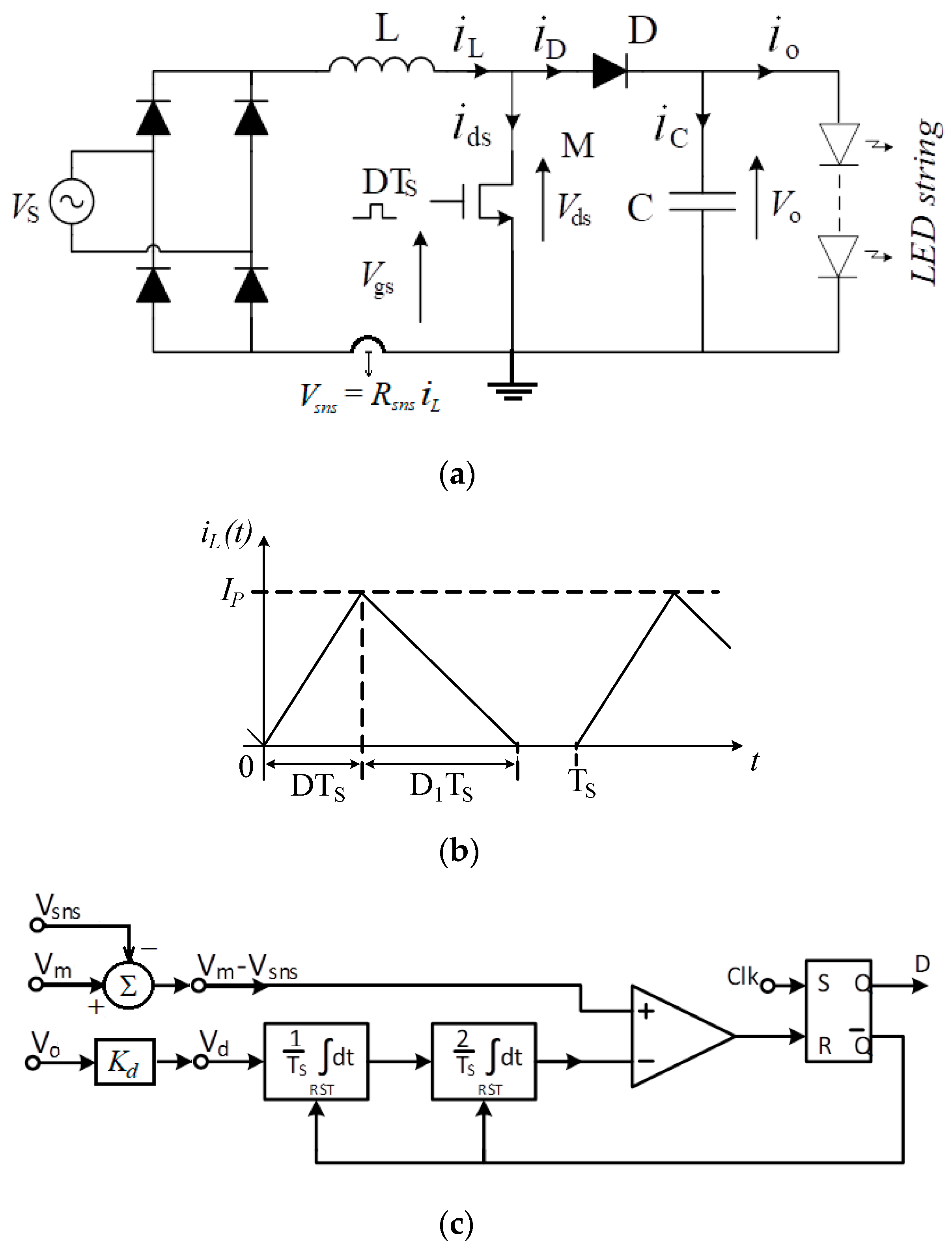
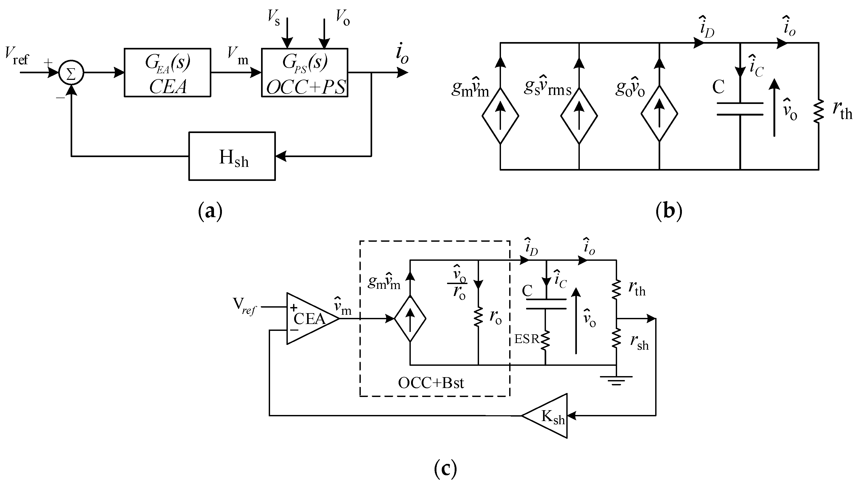
5. Modelling the Control Loop

The OCC DCM boost PFC operates under two feedback loops. The OCC modulator, boost power stage, and inductor current sensing network comprise the inner current loop. The inner current loop shapes the line current according to (12), and thus responds within a switching cycle. As shown in Figure 5a, the outer current loop is comprised of the output current shunt network, Hsh; the current reference, Vref; and the current error amplifier, CEA, which generates the modulation voltage, Vm, for the OCC modulator. The objective of the outer current loop is to regulate the average LED current component, Iodc, while attenuating the second harmonic of the line frequency. To reject the second harmonic of the line frequency, the outer current loop bandwidth has to be severely restricted. For this reason, the outer current loop regards the fast inner loop just as a constant gain system. For the same reason, the slow outer current loop disregards the LED string dynamics. Hence, the low-frequency dynamic model of the LED string is merely a pure resistive term, rth.
The small-signal model of the OCC modulator and the power stage can be derived following the general principles of PFC analysis [27]. First, the large-signal model of the boost diode current is formulated applying power balance considerations
i D ( t ) = P ( t ) V o ( t ) = V R M S 2 ( t ) R e ( V m ( t ) ) V o ( t ) = V R M S 2 ( t ) V o 2 ( t ) R s n s v m ( t )
here, (9) was used.
Next, perturbation and linearization of the large-signal model (27) are performed. This yields the following:
i ^ D = g s v ^ R M S ( t ) + g m v ^ m ( t ) + g o v ^ o ( t )
here, i ^ D ,   v ^ R M S ,   v ^ m ,   a n d   v ^ o are the small-signal perturbations in the boost diode current, the line RMS voltage, the modulating voltage, and the output voltage, respectively. The corresponding gain coefficients are as follows:
g s = i D ( t ) v R M S | v R M S = V R M S = 2 V R M S V m V o 2 R s n s = 2 P a v V o V R M S
g m = i D ( t ) v m | v m = V m = V R M S 2 V o 2 R s n s = P a v V o V m
g o = 1 r o = i D ( t ) v o | v o = V o = 3 V R M S 2 V m V o 3 R s n s = 3 P a v V o 2
Table 1 summarizes the combined small-signal gains of the OCC modulator and the DCM boost PFC operating with an LED string load under a regulated output voltage mode (OVM) as a function of the average output voltage, Vo, and under a regulated output current mode (OCM) as a function of the average output current, Io. The model is shown in Figure 5b. The low-frequency small-signal model of the OCC DCM boost PFC with LED string load can be constructed as shown in Figure 5c, from which the modulating voltage to LED string current transfer function is found.
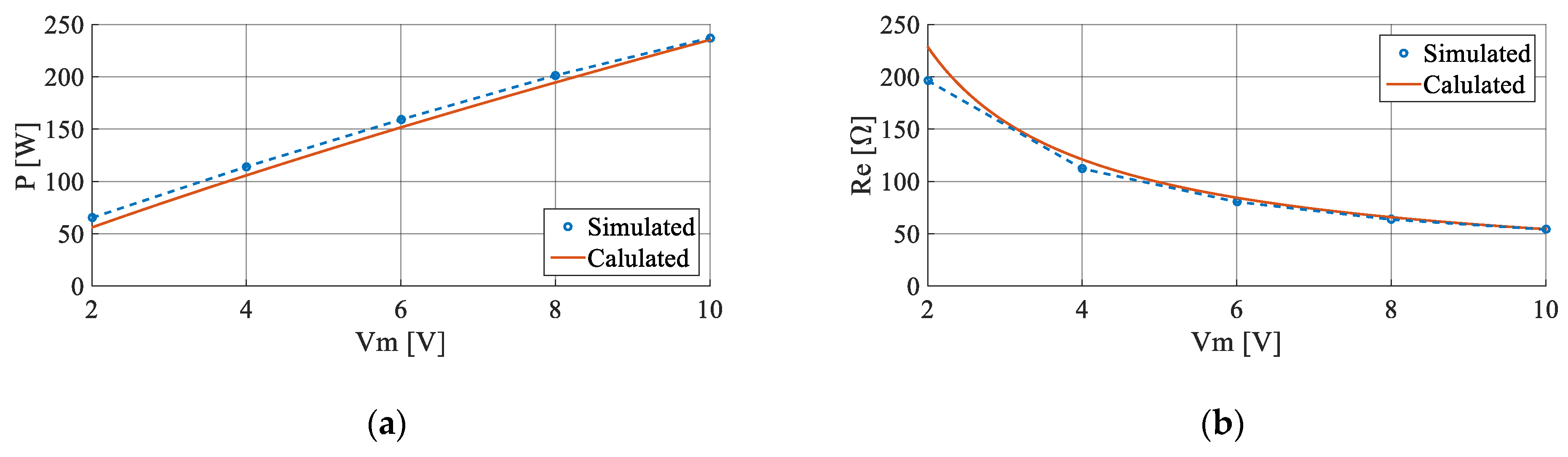
i ^ o v ^ m =   g m r o r t h + r o 1 + s C E S R 1 + s C ( r t h | | r o + E S R )

6. Design Example

The OCC DCM boost PFC can be designed to meet the following specifications: line voltage V r m s = 115   Vac   ( V p k = 160   V ) ; LED load with V t h = 183   Vdc , r t h = 52.5   Ω ; nominal output current I o = 1   A ; nominal power P a v = 235.5   W . The PFC’s switching frequency is f s = 50   kHz .

6.1. Static Design

As the first step, the power stage parameters are determined. To keep the boost converter running in DCM, the boost inductor value shall not exceed the critical inductance value given by
L c r = 1 4 f s V p k 2 P ( 1 V p k V o )
The given specifications yield L c r = 173.83   μ H . Leaving room for component tolerances and transient conditions, the boost inductor is chosen as L = 0.7 L c r = 120   μ H .
The normalized output capacitor value that satisfies the “no noticeable harm” condition can be estimated according to (26) as
C n ( 100 0.08 2 60   ) 2 1 10.37  
As the base capacitance is C b = 1 2 ω L r t h = 1 2 2 π 60 52.5 25.26   μ F , the minimum required value of the output capacitance is C = C n C b 10.37 25.26   μ F = 262   μ F . In practice, C = 270   μ F is selected.
Applying (34), the inductor’s RMS current is I L , R M S = 2.78   [ A ] , the switch RMS current is I T , R M S = 1.82   [ A ] , and the diode RMS current is I D , R M S = 2.1   [ A ] . These were found for the nominal power level.
The input current sensing network is implemented with a cascading a sensing resistor, Rs, a current sensing amplifier, Ksns, and a low pass filter, Hsns(), which is needed to attenuate the current ripple and to provide the averaged sense signal. Thus, the combined gain of the current sensing network is
R s n s ( s ) = v s n s i L ( s ) = R s K s n s H s n s ( s )
The components of the current sensing network can be evaluated by applying the following considerations. The practical dynamic range of the modulating voltage, Vm, is limited by the saturation level of the error amplifier voltage, Vea_sat. Assuming V ea _ sat = 12   V , and leaving some room for transient conditions, the modulation voltage needed to attain the nominal power is about V m = 0.8 V e a _ s a t 10   V . Therefore, the overall low-frequency gain of the sensing network Rsns can be derived from (9) and as a function of the output current, Io:
R s n s = V m V R M S 2 I o P a v 2 2.31  
It is suggested that at full power, the power dissipation in the load current sensing resistor, Rs, be limited to 0.2% of the nominal power, Pav. Hence,
R s = 0.002 P a v I L r m s 2 = 0.061   Ω  
as the RMS current through the sensing resistor equals the inductor current, I L , R M S . A standard value R s = 0.05   Ω was chosen, which also resulted in a bit of a lower power dissipation.
To attain the required value of Rsns, an input current sensing amplifier is needed with a voltage gain of
K s n s = R s n s R s = 46.2  
In practice, the low pass function, Hsns(s), can be realized with the current sensing amplifier. The bandwidth of the filter affects the THD performance of the PFC. Reference [28] suggests that a corner frequency just above 1 kHz is adequate.
A voltage divider can be used to provide the voltage Vd needed for the OCC modulator of the output voltage (see Figure 2c). The required divider ratio can be found from (10)
K d = R sns 2 Lf s 0.193
Another issue to consider is evaluating the output current shunt network (see Figure 5c). Here, the overall current feedback gain is H s h = r s h K s h . To prevent unnecessary power losses, the shunt resistor value, rsh, is chosen, such that its power dissipation is about 0.1% of the power consumption of r t h at full load. This consideration leads to
r s h = r t h 0.001 = 52.5 0.001 = 0.0525
A standard value of r s h = 0.05   Ω was chosen.
Choosing a comfortable value of V r e f = 2.5   V , the desired level of I o = 1   A can be obtained with the shunt voltage gain, K s h , of
K s h = V r e f I o r s h = 2.5 1 0.05 = 50

6.2. Calculation of the Outer Loop Small-Signal Parameters

The outer current loop design is done referring to Figure 5c. The design objectives are to establish the parameters of the shunt amplifier and the current error amplifier for the given (and the derived above) parameters: C o = 100   μ F ; E S R = 4.7   μ Ω ; V t h = 183   Vdc ; r t h = 52.5   Ω ; I o = 1   A ; P a v = 235.5   W ; V m = 10 .
The open-loop small-signal transfer function of the outer loop can be obtained from Figure 5a as
G L ( s ) = H s h G P S ( s ) G E A ( s )
Now the gain coefficients of the combined small-signal modulator and power stage transfer function, GPS(s), are established. The small-signal gain g m is
g m = V s R M S 2 R s n s ( V t h + r t h I o ) 2 = 115 2 2.31 ( 183 + 52.5 1 ) 2 = 0.1 [ 1 Ω ]
whereas the small-signal output resistance r o is
r o = 1 3 ( V t h I o + r t h ) = 1 3 ( 183 1 + 52.5 ) = 78.5 [ Ω ]
As the outer current loop bandwidth is rather low, the effect of the output filter capacitor’s ESR on the outer loop dynamics can be neglected. Hence, according to (32), and using the parameters above, the combined small-signal modulator and power stage transfer function is:
G P S ( s ) = i ^ o v ^ m = 0.1 78.5 52.5 + 78.5 1 1 + s 270 μ 78.5 52.5 78.5 + 52.5 0.06 1 1 + s 1 2 π 18.7
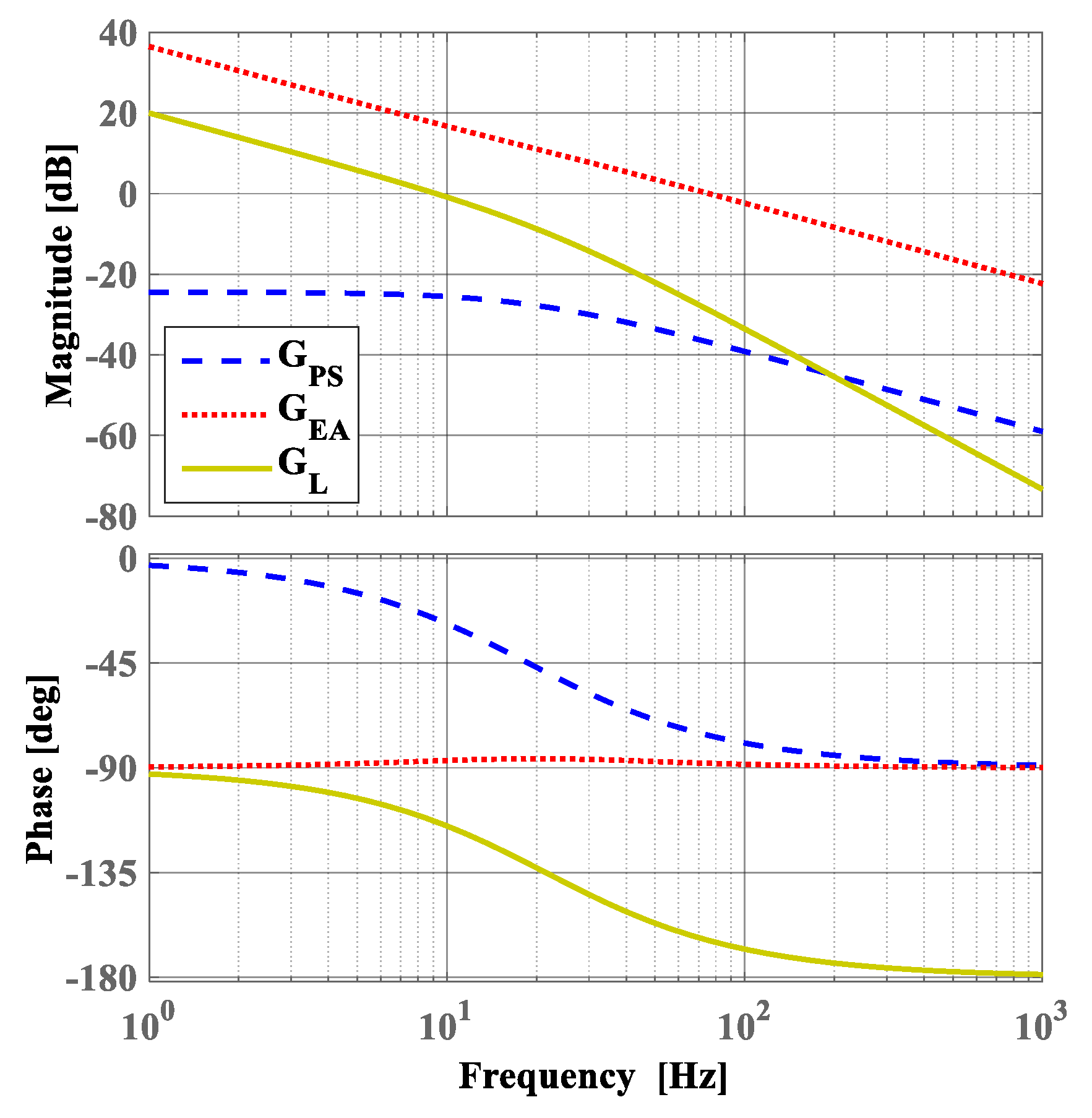
Next, the parameters of the error amplifier are established. A simple outer loop current error amplifier having the following transfer function is sufficient to stabilize the loop
G E A ( s ) = ω 0 s 1 + s ω z 1 + s ω p
The error amplifier’s zero ω z 2 π 18.7   [ r a d s ] is placed to cancel the power stage pole, (see (45)). To suppress the second line harmonic ripple propagating through the current loop, the loop crossover frequency is set to about a decade below the second harmonic frequency: ω c = 2 π ( 10 ) [ r a d s ] 2 π 120 [ r a d s ] = 4 π f L . In order to limit the output current overshoot, the error amplifier’s pole will be set such that P M ( G L ( ω c ) ) = 65 ° .
Note that with the pole-zero cancellation, the open-loop transfer function has only an integrator and a single simple pole, so that its phase margin is
P M ( G L ( ω c ) ) = 180 ° 90 ° tan 1 ( ω c ω p ) = 65 °
Hence, the desired crossover frequency is ω c = 2 π 10 and the pole angular frequency is ω p 2 π 21.45 .
Using (42) and (45), the outer loop gain at the crossover frequency can be approximated by
G L ( ω c ) = H s h G P S ( ω c ) G E A ( ω c ) 15 10 3 2 π ω o = 1
hence ω o 418.88 . Thus, the desired current error amplifier transfer function is as follows:
G E A ( s ) = 418.88 s 1 + s 2 π 18.7 1 + s 2 π 21.45
The resulting frequency responses of the outer current loop gain components are shown in Figure 6.

7. Simulation Results

The OCC DCM boost PFC LED driver design was confirmed by simulation. PSIM simulation software was used. The parameters derived in the design example above were introduced into the program (line voltage V R M S = 115   Vac , V p k = 160   V ; LED load with V t h = 183   Vdc , r t h = 52.5   Ω ; nominal output current I o = 1   A ; nominal power P a v = 235.5   W . The PFC’s switching frequency f s = 50   kHz ). The simulation diagram of the DCM boost PFC with the proposed control circuit is shown in Figure 7.
A simulation was run to confirm the design and to evaluate the performance of the DCM boost PFC with the modified OCC algorithm. Figure 8a illustrates the steady-state key variables of the improved OCC controller at full load. Simulated waveforms of the line voltage, the average power, the output voltage, and the line current are given in Figure 8b. Both the power and the output voltage ripple specifications were reached. The steady-state line current is of a good quality with about 3% THD.
The power relationship (13) and the emulated resistance (5) were compared with the simulated results and are plotted in Figure 9a and Figure 9b, respectively. Excellent agreement between the theoretical predictions and simulation results was found in both cases.

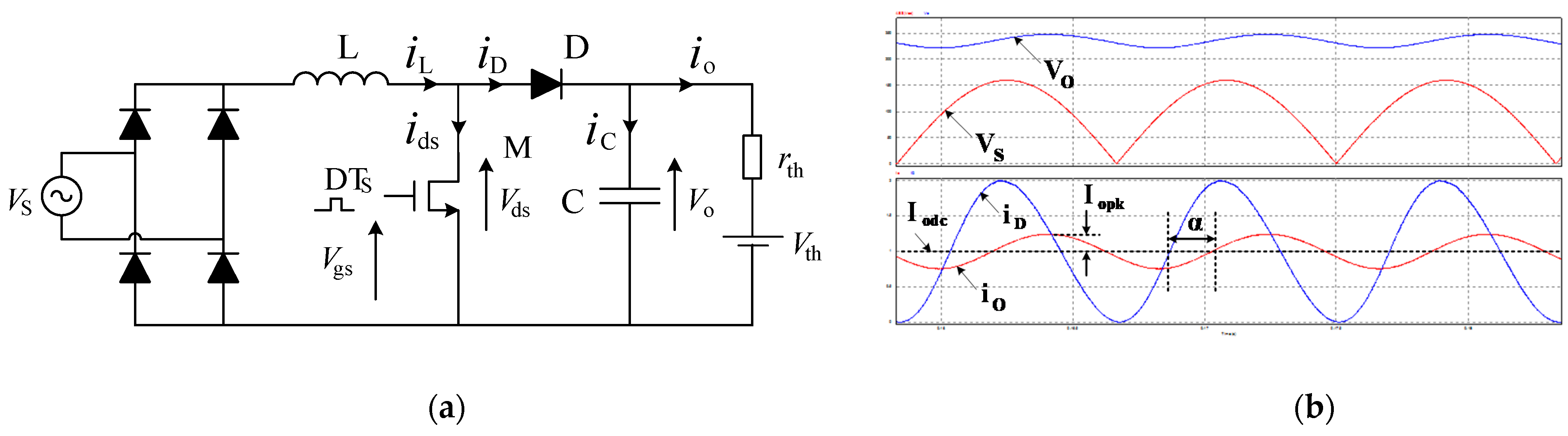
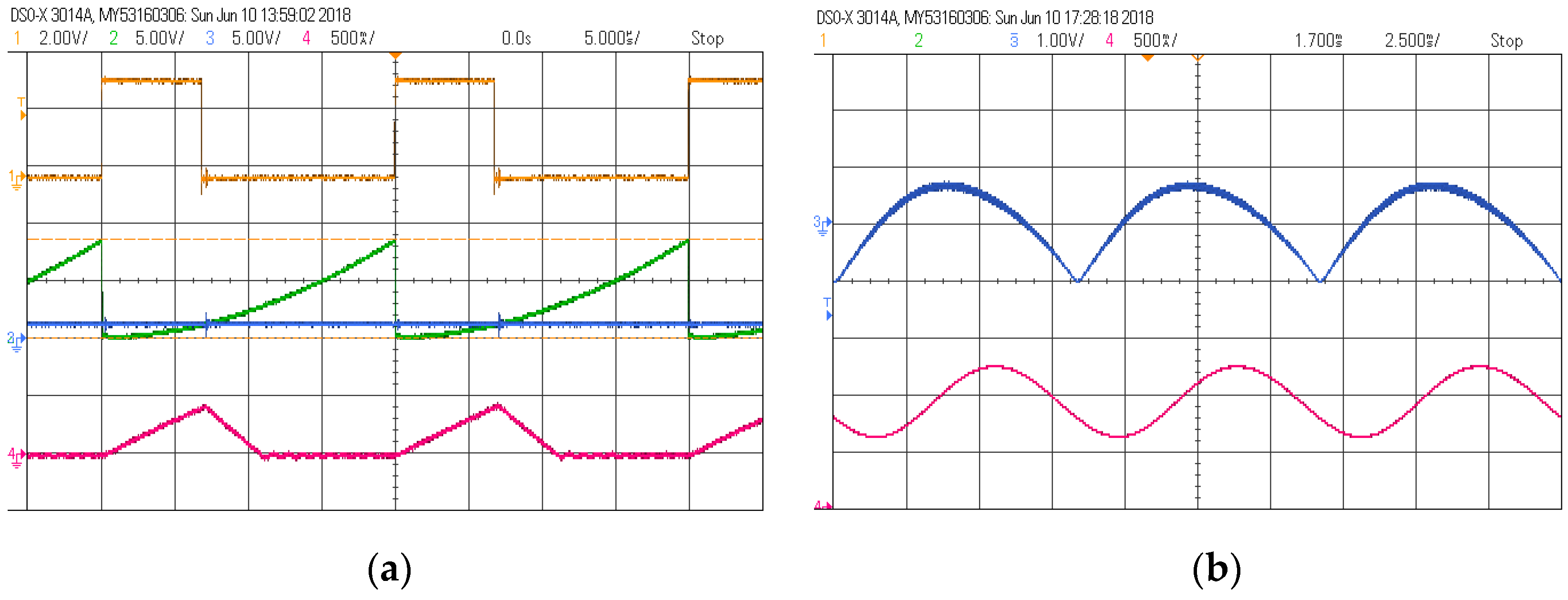
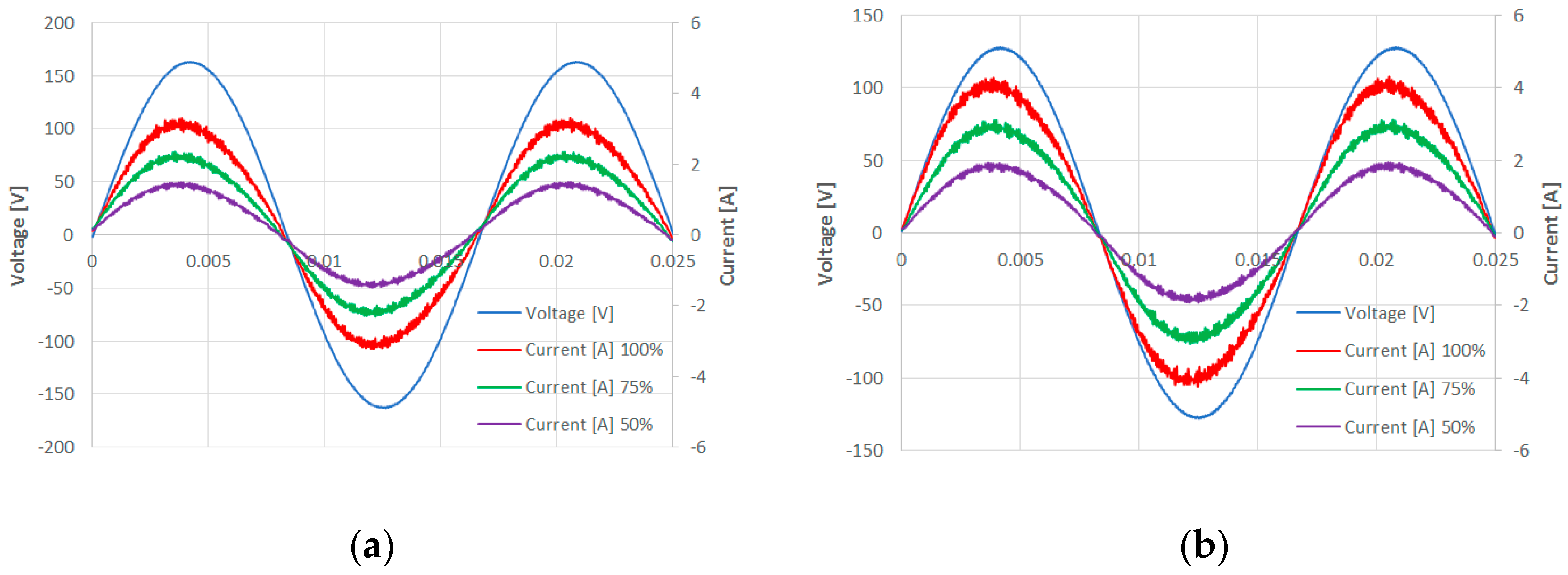
8. Experimental Verification

Experimental DCM boost PFC was designed, built, and tested. The prototype had the following parameters: line voltage Vac = 110 VRMS (60 Hz), output voltage Vo = 230 V dc; and nominal output power Po = 250 W. The boost stage was implemented with L = 120 µH and C = 100 µF, and operated at a switching frequency of fs = 50 kHz. The semiconductors used were: MOSFET switch IPP65R190C7; boost diode DPG10I400PM; rectifier bridge GBU607; bypass diode 6A40G. Series connection of three CXA3590 LED units were used for high power. The non-inverting double integrator within the OCC controller was implemented using trans-conduction amplifier NE5517.
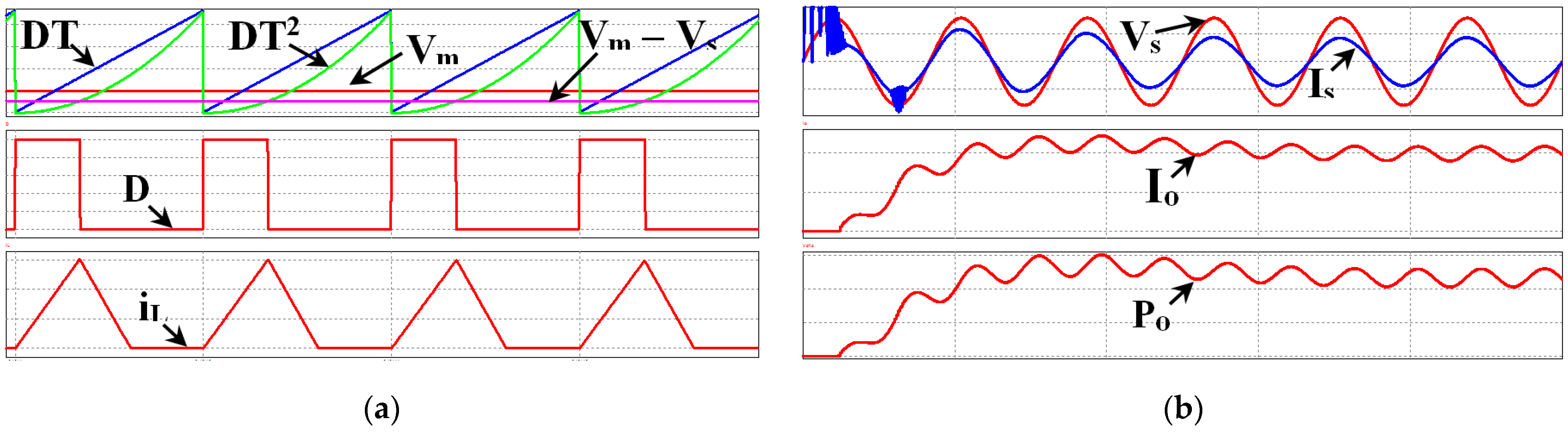
Key experimental waveforms of the DCM boost PFC on the switching frequency scale and the line frequency scale are illustrated in Figure 10 and Figure 11 which show the line voltage and the average line current drawn by the DCM boost PFC, respectively. Testing conditions were line voltage Vac = 110 VRMS; average AC power Po = 250 W; Po=190 W; Po = 125 W. The measured total harmonic distortion in the line current was THDI = 4.3%, and the measured power factor (PF) = 0.995.
THD performance of the proposed PFC rectifier/LED driver depends primarily on three factors: the accuracy of the current sensing network averaging performance (because of the limited switching noise filtering and its inherent phase shift), the accuracy of duty cycle generation by the OCC modulator, and the propagation of the second harmonic ripple within the control loop (which appears as v2 term superimposed on the true modulation voltage, Vm). As a result, in practice, somewhat corrupted modulation voltages are presented to the OCC modulator and generate distortion. Accordingly, 3% THD was predicted by simulation, whereas the measured experimental value was just a bit higher at 4.5%.
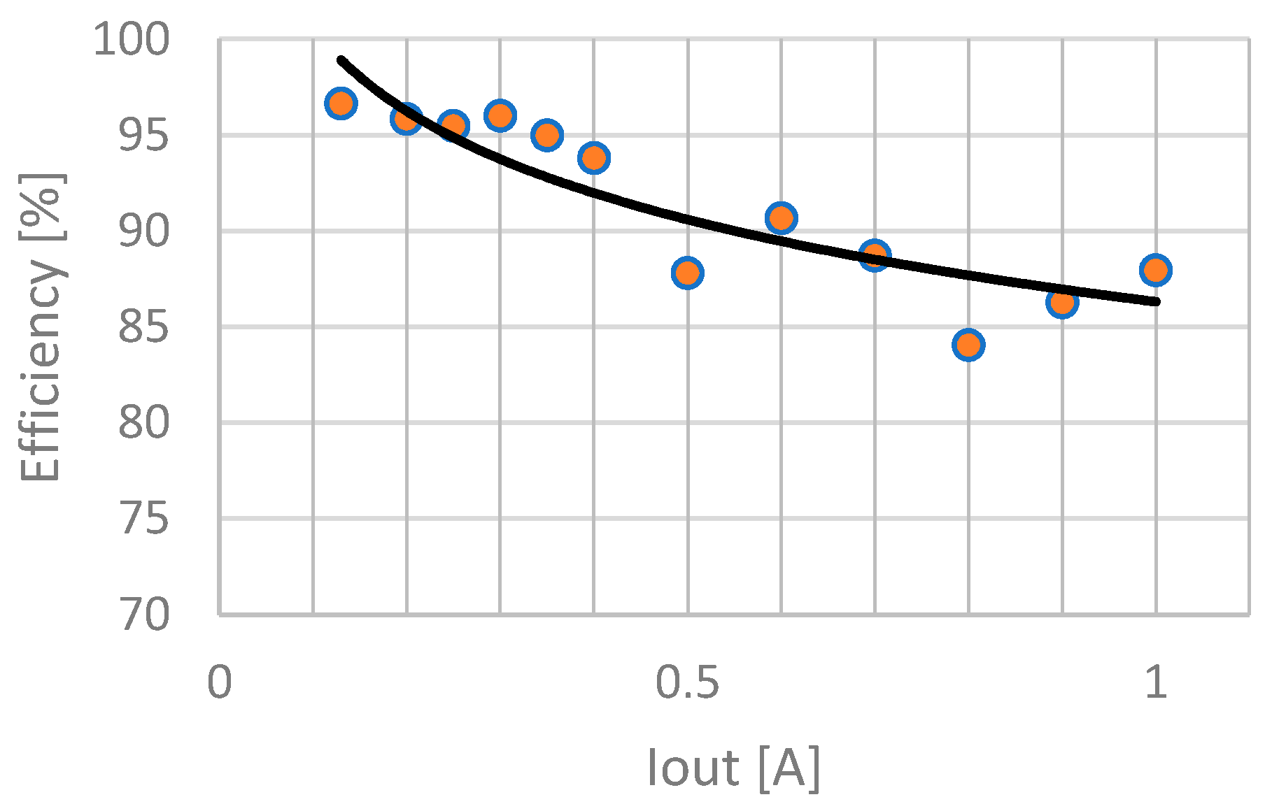
As the experimental work was aimed at verifying the OCC control law (11) and its implementation, little consideration was given to the efficiency issues. The experimental prototype relied on hard switching and used no snubbers. Yet, an acceptable performance was obtained. The efficiency plot of the experimental prototype at nominal voltage and full power is presented in Figure 12.

9. Conclusions

This work was inspired by an earlier counterpart [19], which suggested a feedforward type of an OCC modulation scheme for a DCM boost PFC rectifier. This paper is aimed to improve the small-signal characteristics of the original circuit. Here, a current feedback OCC scheme was investigated to control the DCM boost PFC rectifier. As an application example, the improved PFC rectifier was employed as a high brightness high power LED driver; however, it could also be used for other applications. In the paper, the improved control law and other key theoretical considerations of the current mode OCC DCM boost PFC were derived, analyzed, and successively applied to the design of an experimental prototype. A method of design for minimum THD was also suggested. The reported theoretical predictions stand in good agreement with the simulation and the experimental results. The experimental prototype was proven to be rather robust.
The primary advantage of the proposed scheme over the earlier counterpart [19] is in the linear dependence of power on modulating voltage. As a result, the average small-signal gains of the average model are linear. Hence, the system is robust and easier to design. Furthermore, in comparison with recently reported work of [29,30], the proposed controller is simple to implement.

Author Contributions

Conceptualization, D.S.; Formal analysis, A.A.; Investigation, T.T. All authors have read and agreed to the published version of the manuscript.

Funding

This research received no external funding.

Institutional Review Board Statement

Not applicable.

Informed Consent Statement

Not applicable.

Conflicts of Interest

The authors declare no conflict of interest.

References

  1. LED Lighting, DOE Brochure. Available online: https://energy.gov/energysaver/led-lighting (accessed on 31 August 2021).
  2. Limits-Limits for Harmonic Current Emissions (Equipment Input Cur-rent ≤16 A per Phase), IEC 61000-3-2, 2010, EMC Part 3-2. Available online: https://webstore.iec.ch/preview/info_iec61000-3-2%7Bed5.1%7Den.pdf (accessed on 31 August 2021).
  3. Singer, S. Gyrators Application in Power Processing Circuits. IEEE Trans. Ind. Electron. 1987, IE-34, 313–318. [Google Scholar] [CrossRef]
  4. Shmilovitz, D.; Yaron, I.; Singer, S. Transmission-line-based gyrator. IEEE Trans. Circuits Syst. I Fundam. Theory Appl. 1998, 45, 428–433. [Google Scholar] [CrossRef]
  5. Cid-Pastor, A.; Martinez-Salamero, L.; Alonso, C.; Estibals, B.; Alzieu, J.; Schweitz, G.; Shmilovitz, D. Analysis and design of power gyrators in sliding-mode operation. IEE Proc.-Electr. Power Appl. 2005, 152, 821–826. [Google Scholar] [CrossRef]
  6. Shmilovitz, D. Gyrator realization based on a capacitive switched cell. IEEE Trans. Circuits Syst. II Express Briefs 2006, 53, 1418–1422. [Google Scholar] [CrossRef]
  7. Garcia, O.; Cobos, J.; Prieto, R.; Alou, P.; Uceda, J. Single phase power factor correction: A survey. IEEE Trans. Power Electron. 2003, 18, 749–755. [Google Scholar] [CrossRef] [Green Version]
  8. Lee, J.J.; Kwon, J.M.; Kim, E.H.; Choi, W.Y.; Kwon, B.H. Single-Stage Single-Switch PFC Flyback Converter Using a Synchronous Rectifier. IEEE Trans. Ind. Electron. 2008, 55, 1352–1365. [Google Scholar]
  9. Yao, K.; Fu, X.; Lv, J. DCM Flyback PFC converter with optimum utilization control of switching cycles. In Proceedings of the 2015 IEEE Energy Conversion Congress and Exposition (ECCE), Montreal, QC, Canada, 20–24 September 2015; pp. 2445–2452. [Google Scholar]
  10. Liu, K.H.; Lin, Y.L. Current waveform distortion in power factor correction circuits employing discontinuous-mode boost converters. In Proceedings of the 20th Annual IEEE Power Electronics Specialists Conference, Milwaukee, WI, USA, 26–29 June 1989; Volume 2, pp. 825–829. [Google Scholar] [CrossRef]
  11. Lai, J.S.; Chen, D. Design consideration for power factor correction boost converter operating at the boundary of continuous conduction mode and discontinuous conduction mode. In Proceedings of the Proceedings Eighth Annual Applied Power Electronics Conference and Exposition, San Diego, CA, USA, 7–11 March 1993; pp. 267–273. [Google Scholar]
  12. Rossetto, L.; Spiazzi, G.; Tenti, P. Control Techniques for Power Factor Correction, PEMC94. Available online: http://www.dei.unipd.it/~pel/Articoli/1994/Pemc/Pemc94.pdf (accessed on 31 August 2021).
  13. Gegner, J.P.; Lee, C.Q. Linear peak current mode control: A simple active power factor correction control technique for continuous conduction mode. In Proceedings of the 27th Annual IEEE Power Electronics Specialists Conference, Baveno, Italy, 23–27 June 1996; Volume 1, pp. 196–202. [Google Scholar]
  14. Rajagopalan, J.; Lee, F.C.; Nora, P. A generalized technique for derivation of average current mode control laws for power factor correction without input voltage sensing. In Proceedings of the APEC 97-Applied Power Electronics Conference, Atlanta, GA, USA, 27 February 1997; Volume 14, pp. 663–672. [Google Scholar]
  15. Maksimovic, D.; Jang, Y.; Erickson, R.W. Nonlinear-carrier control for high-power-factor boost rectifiers. IEEE Trans. Power Electron. 1996, 11, 578–584. [Google Scholar] [CrossRef]
  16. Orabi, M.; Haron, R.; El-Aroudi, A. Comparison between Nonlinear-Carrier Control and Average-Current-Mode Control for PFC Converters. In Proceedings of the 2007 IEEE Power Electronics Specialists Conference, Orlando, FL, USA, 17–21 June 2007; pp. 1349–1355. [Google Scholar]
  17. Lai, Z.; Smedley, K.M. A family of continuous-conduction-mode power-factor-correction controllers based on the general pulse-width modulator. IEEE Trans. Power Electron. 1998, 13, 501–510. [Google Scholar] [CrossRef]
  18. Qiao, C.; Smedley, K.M.; Lai, Z.; Nabant, M. An improved integration-reset controlled single-phase unity-power-factor boost rectifier with lower distortion. In Proceedings of the IEEE 25th Annual Conference of the IEEE Industrial Electronics Society, San Jose, CA, USA, 29 November–3 December 1999; pp. 272–277. [Google Scholar]
  19. Lai, Z.; Smedley, K.M.; Ma, Y. Time quantity one-cycle control for power-factor correctors. IEEE Trans. Power Electron. 1997, 12, 369–375. [Google Scholar] [CrossRef]
  20. Etz, R.; Patarau, T.; Petreus, D. Comparison between digital average current mode control and digital one cycle control for a bridgeless PFC boost converter. In Proceedings of the 2012 IEEE 18th International Symposium for Design and Technology in Electronic Packaging (SIITME), Alba Iulia, Rumania, 25–28 October 2012; pp. 211–215. [Google Scholar]
  21. Li, Y.; Yang, Y.; Zhu, Z.; Qiang, W. Zero-crossing distortion analysis in one-cycle controlled boost PFC for Low THD. In Proceedings of the 2011 9th IEEE International Conference on ASIC, Xiamen, China, 25–28 October 2011; pp. 661–664. [Google Scholar]
  22. ElAroudi, A.; Giral, R.; Maixe, J.; Calvente, J.; Martinez-Salamero, L. Novel autonomous current mode one-cycle controller for PFC AC-DC pre-regulators. In Proceedings of the 2005 European Conference on Circuit Theory and Design, Cork, Ireland, 2 September 2005; Volume 3, pp. III/51–III/54. [Google Scholar] [CrossRef]
  23. Ruiz-Magaz, G.; Giral, R.; Calvente, J.; Vidal-Idiarte, E.; Romero, A. Predictive one-cycle current control of a boost converter. In Proceedings of the 2012 15th International Power Electronics and Motion Control Conference (EPE/PEMC), Novi Sad, Serbia, 4–6 September 2012. [Google Scholar]
  24. Nimesh, V.; John, V. Comparison of one cycle control of charge and current for bi-directional boost rectifiers. In Proceedings of the 2012 IEEE International Conference on Power Electronics, Drives and Energy Systems (PEDES), Bengaluru, India, 16–19 December 2012; pp. 1–6. [Google Scholar]
  25. Jappe, T.K.; Mussa, S.A. Discrete-time one cycle control technique applied in single-phase PFC boost converter. In Proceedings of the 2011 IEEE International Symposium on Industrial Electronics, Gdansk, Poland, 27–30 June 2011; pp. 1555–1560. [Google Scholar]
  26. Lehman, B.; Wilkins, A.J. Designing to Mitigate Effects of Flicker in LED Lighting: Reducing risks to health and safety. IEEE Power Electron. Mag. 2014, 1, 18–26. [Google Scholar] [CrossRef]
  27. Erikson, R.; Maksimovic, D. Fundamentals of Power Electronics, 2nd ed.; Chapman and Hall: New York, NY, USA, 1997. [Google Scholar]
  28. Abramovitz, A.; Ben-Yaakov, S. Current spectra translation in single phase rectifiers: Implications to active power factor correction. IEEE Trans. Circuits Syst. I Fundam. Theory Appl. 1997, 44, 771–775. [Google Scholar] [CrossRef]
  29. Clark, A.C.W.; Musavi, F.; Eberle, W. Digital DCM Detection and Mixed Conduction Mode Control for Boost PFC Converters. IEEE Trans. Power Electron. 2014, 29, 347–355. [Google Scholar] [CrossRef]
  30. Yao, K.; Hu, W.; Li, Q.; Lyu, J. A novel control scheme of DCM boost PFC converter. IEEE Trans. Power Electron. 2015, 30, 5605–5615. [Google Scholar] [CrossRef]
Figure 1. DCM boost PFC rectifiers with: (a) an earlier feed-forward OCC controller and (b) proposed current mode OCC controller.
Energies 14 05486 g001
Figure 2. The topology of the boost PFC rectifier / LED driver (a), illustration of the boost inductor current in DCM (b), and improved OCC PWM modulator scheme for the current mode DCM boost PFC rectifiers (c).
Energies 14 05486 g002
Figure 3. (a) DCM Boost PFC/ LED driver with the LED string represented by its Thevenin equivalent circuit; (b) simulated voltage and average current waveforms.
Energies 14 05486 g003
Figure 4. Peak LED string current ripple as a function of the normalized output capacitance.
Energies 14 05486 g004
Figure 5. Simplified low frequency dynamic models of the outer current loop of the OCC DCM boost PFC with LED string load: (a) conceptual model; (b) combined modulator and power stage model; (c) small-signal model used for stability analysis of the output current mode operation of the LED-string load.
Energies 14 05486 g005
Figure 6. Frequency response of the outer current loop components (OCCs): modulator and power stage (GPS); error amplifier (GEA); the loop gain (GL).
Energies 14 05486 g006
Figure 7. PSIM simulation diagram of the DCM boost PFC with the improved OCC control circuit (design example).
Energies 14 05486 g007
Figure 8. Simulated waveforms of the OCC DCM boost PFC (design example): (a) key OCC modulator variables; (b) the line voltage, the average power, the output voltage, and the line current at full power.
Energies 14 05486 g008
Figure 9. Comparison of the theoretically predicted and simulated results for: (a) power level Pout(Vm); (b) emulated resistance Re(Vm) as a function of modulated voltage, Vm.
Energies 14 05486 g009
Figure 10. Experimental waveforms of the modified OCC DCM boost PFC rectifier. (a) At the switching frequency scale (horizontal scale 5 uS/div): blue—the control voltage, Vc; green—the quadratic ramp; yellow—the gating voltage, Vgs; red—the inductor current; (b) at the line frequency scale (horizontal scale−2.5 mS/div): blue–the sensed (and filtered) input current signal, Vsns; red—the LED current. (Vertical scale of each trace is found in the upper left corner).
Energies 14 05486 g010
Figure 11. Line voltage, Vac, and the average line current, Iac, of the experimental prototype at different line voltages: (a) Vac rms = 115 v; (b) Vac rms = 90 v; Po = 250 W; Po = 190 W; Po = 125 W.
Energies 14 05486 g011
Figure 12. The efficiency of the experimental prototype DCM boost PFC.
Energies 14 05486 g012
Table 1. Outer loop gain coefficients.
OVMOCM
g s 2 P a v V o V R M S 2 I o V R M S
g m P a v V o V m V R M S 2 R s n s ( V t h + r t h I o ) 2
r o = 1 g o V o 2 3 P a v 1 3 ( r t h + V t h I o )
Publisher’s Note: MDPI stays neutral with regard to jurisdictional claims in published maps and institutional affiliations.

