Article

Closed-Form Formulas for Automated Design of SiC-Based Phase-Shifted Full Bridge Converters in Charger Applications

Institute of Control and Industrial Electronics, Warsaw University of Technology, 00-662 Warsaw, Poland
*
Author to whom correspondence should be addressed.
Energies 2021, 14(17), 5380; https://doi.org/10.3390/en14175380
Submission received: 12 May 2021 / Revised: 26 July 2021 / Accepted: 24 August 2021 / Published: 30 August 2021
(This article belongs to the Special Issue Control and Topologies of Grid Connected Converters)

Abstract

:
Phase-Shifted Full Bridge (PSFB) topology in its four-diode variant is the choice with the lowest part count in applications that demand high power, high voltage, and galvanic isolation, such as in Electric Vehicle (EV) chargers. Even though the topology is prevalent in power electronics applications, no single, unified analytical model has been proposed for the design process of four-diode PSFB converters. As a result, engineers must rely on simulations and empirical results obtained from previously built converters when selecting components to properly match the DC source voltage level with the DC load voltage requirements. In this work, the authors provide a design-oriented analysis approach for obtaining the output voltage and semiconductor current values, ready for implementation in a spreadsheet- or MATLAB-type software to automate design optimization. The proposed formulas account for all the first-order nonlinear dependencies by considering the impact of each of the following eight design parameters: DC-link voltage, load resistance, phase-shift ratio, switching frequency, transformer turns ratio, magnetizing inductance, series inductance, and output inductance. The results are verified through experiments at the power level of 10 kW and the DC-link voltage level of 800 V by using a grid simulator and a SiC-based two-level Active Front End (AFE) with a DC–DC stage based on the PSFB topology. The accuracy of the output voltage formula is determined to be around 99.6% in experiments and 100.0% in simulations. Based on this exact model, an automated design procedure for high-power high-voltage SiC-based PSFB converters is developed. By providing the desired DC-link voltage, output voltage, output power, output current ripple factor, maximum temperatures, and semiconductor and heatsink databases, the algorithm calculates a set of feasible designs and points to the one with the lowest semiconductor losses, dimensions, or cost.

1. Introduction

With the rapidly growing share of Electric Vehicles (EVs) in the overall vehicle market, the numbers of required On-Board Chargers (OBCs) and DC fast chargers are expected to rise at an unprecedented rate. To meet that demand, automated design tools [1] will be necessary, especially for the more complex stage of a charger—the isolated DC–DC converter. In contrast to the plethora of new topologies that feature an increasingly high component count, the Phase-Shifted Full Bridge (PSFB) effectively combines the relative simplicity of a bridge converter with the benefits of zero-voltage switching (ZVS) without the need for resonant tanks [2]. The four-diode variant is well-suited for high-voltage operation (as opposed to the two-diode variant [3]) and, if equipped with SiC devices, it can also accommodate high switching frequencies [4]. The PSFB, in conjunction with a three-phase two-level Active Front End (AFE), allows AC–DC transfer of electric energy at high power and voltage levels while providing galvanic isolation and requiring a minimum number of components.
This specification enables the two converters to operate together in applications such as EV chargers [5] (see Figure 1a) or photovoltaic (PV) inverters [6] (see Figure 1b). In such configurations, the AFE provides a power factor correction feature [7,8,9], while the PSFB is responsible for the DC voltage control. Sample specification requirements for an EV charger are presented in Table 1.
While the selection of components for the AFE is relatively straightforward and the relationship between the input (grid) voltage Vabc and the dc-link voltage Vdc is simple, the same is not the case with regard to the PSFB part of the charger. The output voltage Vo has an intricate dependence on eight design parameters: Vdc, load resistance Ro, phase-shift ratio φ, switching frequency fs, transformer turns ratio n, magnetizing inductance Lm, series inductance Ll, and output inductance Lo; however, the literature provides no closed-form formulas that encompass all of these dependencies. So far, one approach to this problem has been to design the converter based on some very approximate calculations and then to let the voltage controller set φ to obtain the desired value of Vo. However, the problem is that for many combinations of the design parameters there is simply no value of φ that leads to a particular required Vo value at the given output power level (Po). Additionally, if the converter does work at the required voltage and power conditions, it is certain to be overdesigned, which implies unnecessarily high losses, dimensions, and costs. Another, more prevalent method is to conduct simulations at the required Vdc, Vo, and Po values [10]. This is a valid but not scalable solution, i.e., it cannot be efficiently automated for multi-objective optimization of the design.
For that, one needs closed-form expressions, which enable a spreadsheet- or MATLAB-type software to calculate various solutions quickly, based only on a closed set of design parameters. Some advanced mathematical models related to the output voltage and losses were presented in the literature; however, these concerned the two-diode PSFB version, which is suited for low-voltage applications [11,12,13,14,15]. Research was also performed in the area of the PSFB with a voltage doubler [16], and even though this topology is well-suited for high-voltage applications, it lacks in power throughput. Many analyses for resonant variants of PSFB were conducted [17,18,19], including the development of an accurate output voltage formula reported for the LLC Full-Bridge topology [20]. As for the four-diode PSFB, only non-closed-form expressions have been provided, such as the ones in [2], which, in addition, do not consider the impact of all eight design parameters. Similar formulas later appeared in other works related to PSFB modeling [21,22,23]; however, the problem remains unsolved—if an engineer wants to accurately calculate the output voltage, closed-form expressions are required—otherwise it is not feasible. There is a similar situation regarding the PSFB loss calculations, where it is common to provide general loss formulas without stating how the related rms and average semiconductor current values were calculated [24,25]. Recently, a thorough analytical investigation was presented [26] that outlined the relationship between the output voltage and the parasitic components of the PSFB, which cause certain second-order effects. However, it is the first-order, verified relationships between the values of main components that are primarily required for the design automation.
This publication takes a deep dive into analytical expressions for the four-diode PSFB topology related to output voltage and semiconductor currents that are required for an automated design procedure. Section 2 presents the conducted analysis and compares results obtained from the developed expression to those from simulations. This section also shows the derivation of resulting semiconductor-related current formulas, which are vital for enabling a loss-based automated semiconductor selection process. Furthermore, control methods for both AFE and PSFB are discussed, including their implementation. In Section 3, the laboratory setup is discussed and the results of steady-state experiments are shown and analyzed. As demonstrated in Figure 2, the analytical model based on the eight design parameters is first developed throughout Formulas (1)–(36) and then the resulting expressions for output voltage (37) and semiconductor-related currents (41), (42), (46), (47) are verified. Upon this verification, automated design procedure for the four-diode PSFB is presented for the first time, based on the presented analytical model. Using only the knowledge of the application requirements and the devices available, selection of components and parameters is automated to take into consideration voltage level issues, output current continuity, and semiconductor temperatures calculated based on accurate loss formulas. In Section 4, conclusions are drawn regarding the applicability of the developed expressions and the potential of this approach for computer-aided design automation.

2. Materials and Methods

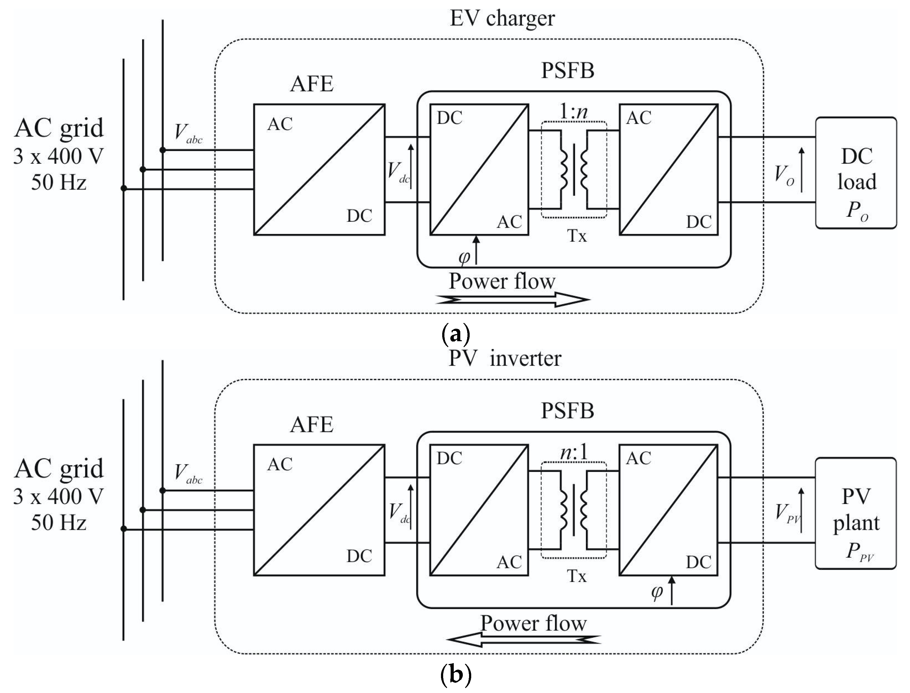
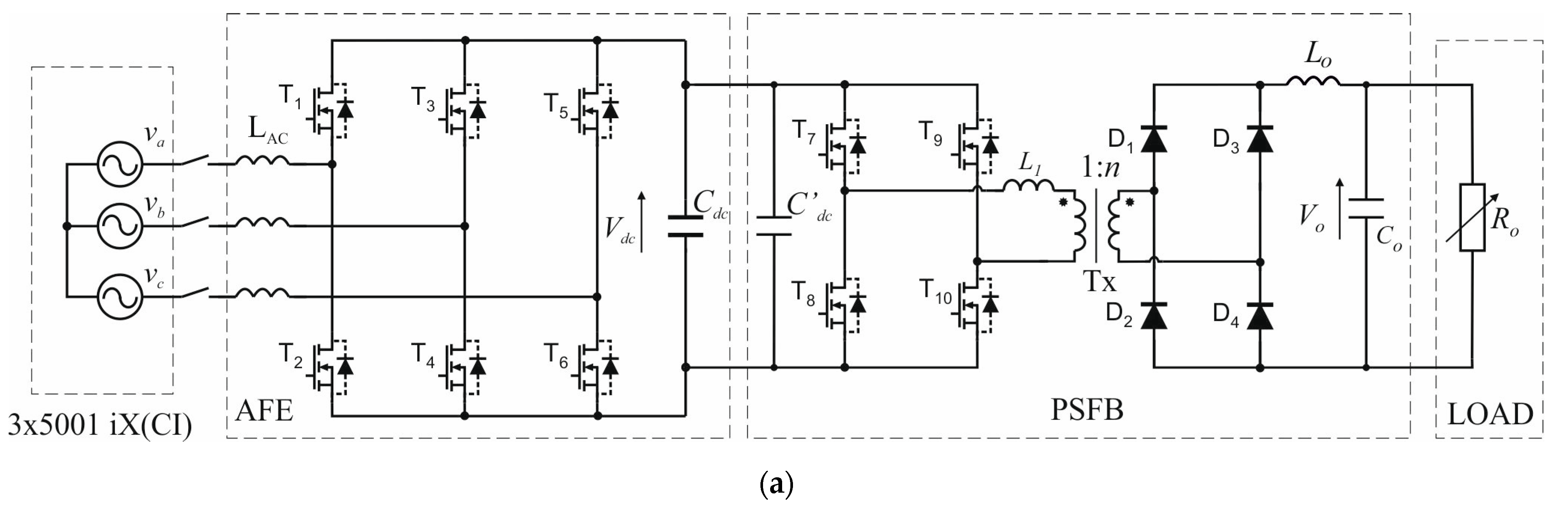
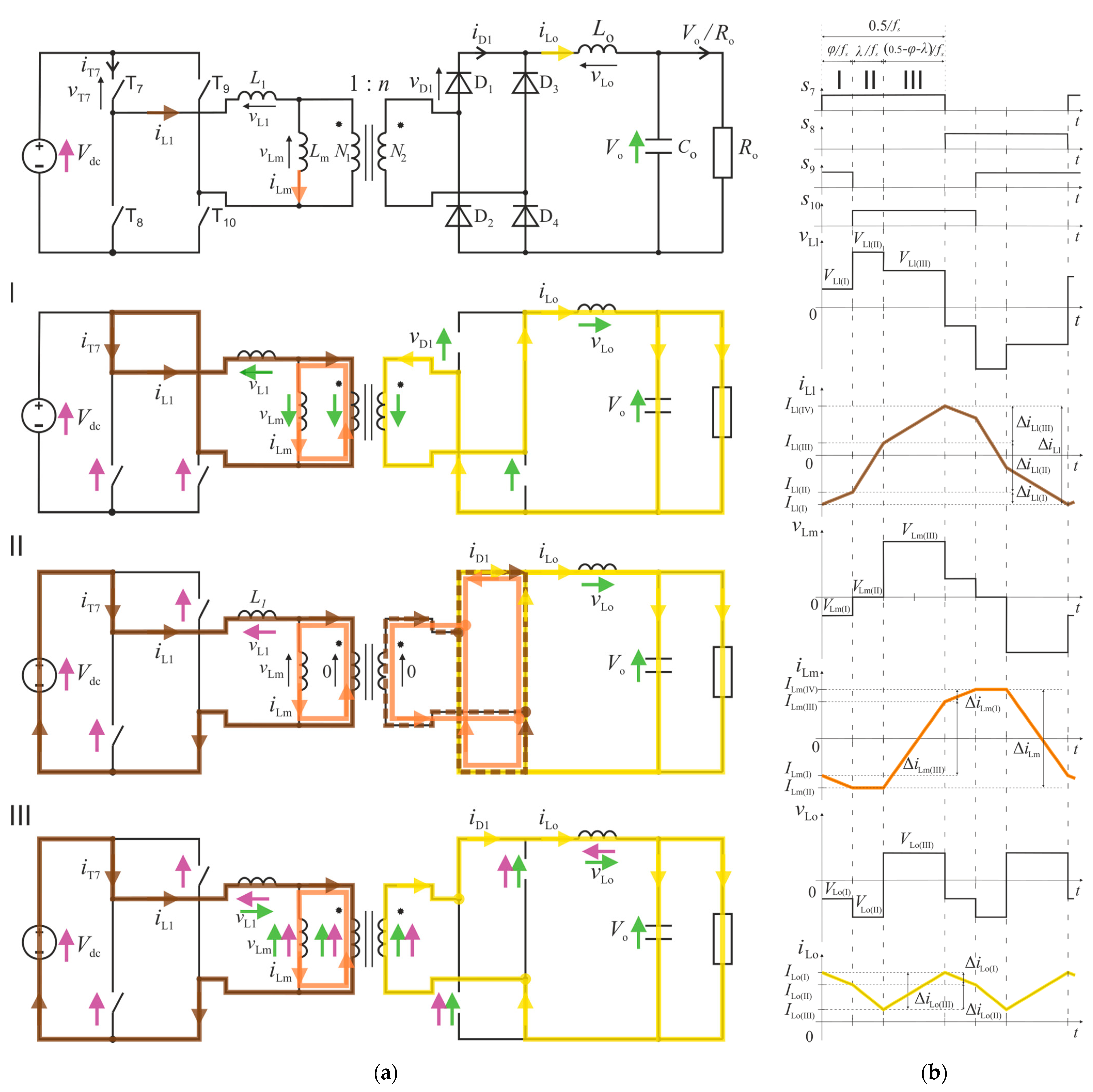
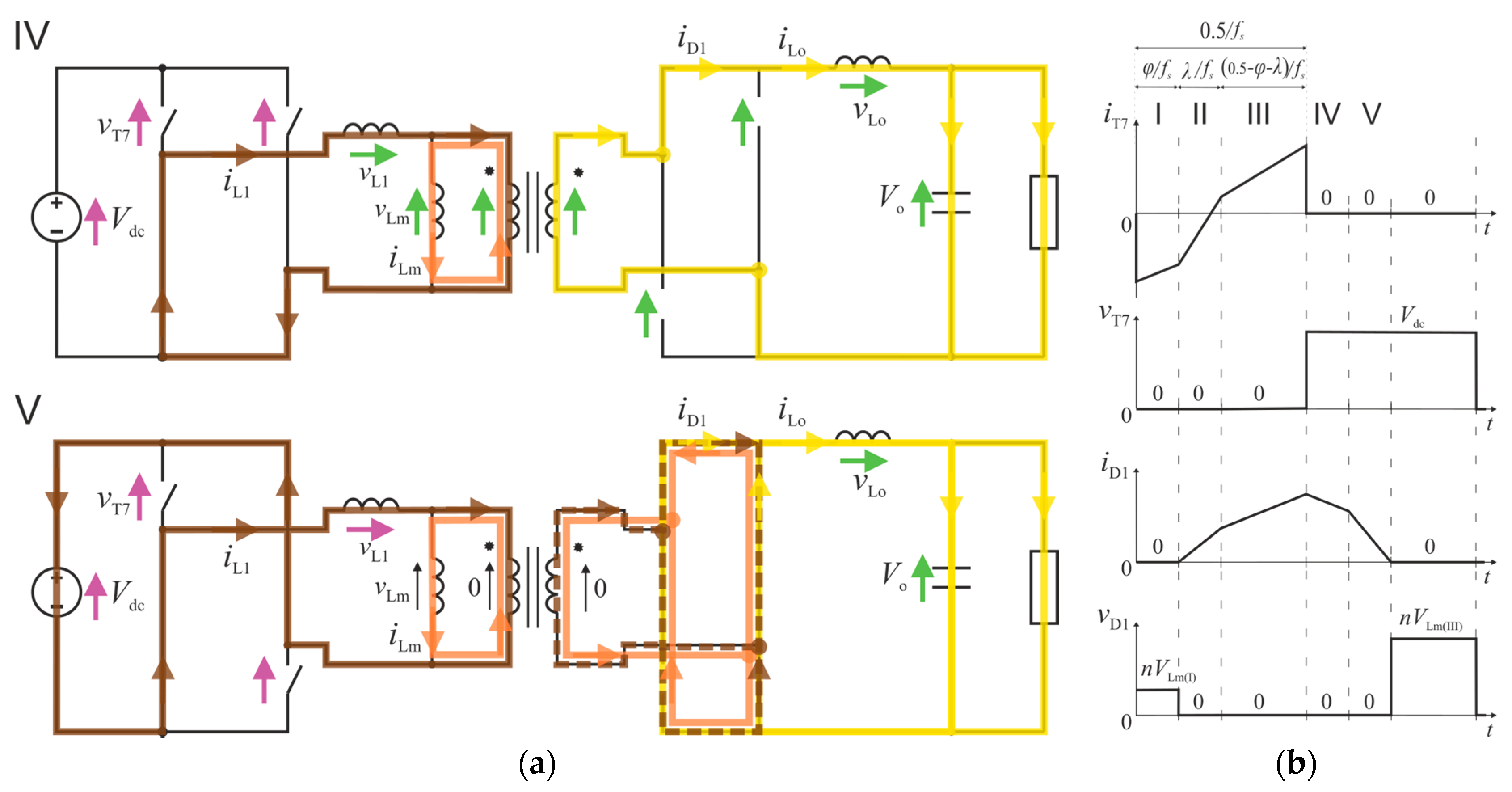
2.1. Topological Details

The two-stage charger with its topological details is shown in Figure 3a. The AFE consists of three input inductors (LAC), six SiC MOSFETs (T1–T6), as well as a DC-link capacitor (Cdc). The PSFB consists of a transformer with turns ratio n and magnetizing inductance Lm, two inductors (Ll, Lo), four SiC MOSFETs (T7–T10), four SiC diodes (D1–D4), and two capacitors (Cdc′, Co). As depicted in Figure 3b, the AFE controller takes in six measurements (input currents ib and ic, input voltages va, vb, and vc, and the DC-link voltage vdc) and provides six control signals (s1s6). On the other hand, the PSFB controller requires one measurement (output voltage vo) and provides four control signals (s7s10). The role of the inductor Ll should be elaborated here: in certain operating conditions, its presence is not necessary. The converter can operate using only the energy accumulated in the magnetic field of the primary-side leakage inductance of the transformer to charge and discharge parasitic output capacitances of the switches [27,28]. However, at light-load high-voltage conditions that magnetic energy might be insufficient [29], and the result may be not only lower efficiency due to lack of zero-voltage switching but also the destruction of the transistors due to entering undesirable off-states, in which DC-link voltage is almost evenly divided between the high-side and the low-side switch.

2.2. Topology Analysis

The PSFB converter can be analyzed in the following way by means of averaging inductor voltage waveforms and the AC component of the output inductor current (capacitor current), and equating these averaged values to zero. Due to the multitude of significant parameters, all of which are interacting with each other, the entire derivation process takes a couple of pages. For clarity, only the initial analysis stage and the final results that can be readily implemented into a spreadsheet or other similar software are presented. It should be noted that the derived formula has a closed form, i.e., it contains only specification parameters that are provided to an engineer and design parameters that must be selected by the engineer. These parameters are DC-link voltage (Vdc), load resistance (Ro), phase shift ratio (φ), switching frequency (fs), transformer turns ratio (n), magnetizing inductance (Lm), series inductance (Ll), and output filter inductance (Lo). These parameters can be observed throughout Figure 4.
Figure 4a presents equivalent circuits of the PSFB in three main, independent states that can be reached (I–III). These states correspond directly to the control signal configurations (s7s10) shown in Figure 4b, and have the total duration of half of the switching period 1/fs. Note that the remaining three states are not discussed here since inductor-related waveforms in the second half of the switching period are symmetrical to those in the first half. Furthermore, due to its relatively low value in SiC applications (c.a. 100 ns), deadtime is omitted, and additional states resulting from it are not considered.

2.2.1. State I Analysis

In state I (with duration of φ/fs) it can be observed that there is no energy transfer from the DC-link to the load. Magnetic energy accumulated in various inductances is redistributed between these inductances and between them and the load. The exact nature of the energy flow is dictated by how voltage is shared among these inductances. Voltage Vo, which is kept constant by the output capacitor Co, is divided between the transformer and the output inductor proportionally, as resulting from the inductance values and the turns ratio. It should be noted that, starting from (1), only the eight aforementioned design parameters are used, and, as in the case of (2), the previously defined expressions. Thereby, final expressions will also depend exclusively on the design parameters set. The levels of voltage applied during state I across inductances Lm (VLm(I)), Ll (VLl(I)), and Lo (VLo(I)) can be obtained in the following manner:
V L m ( I ) = V o · n · L l · L m L l · L m · n 2 + L o · ( L l + L m )
V L l ( I ) = V L m ( I )
V L o ( I ) = V o · L o L o + L l · L m · n 2 L l + L m
Given the polarities of the voltage applied across the particular inductances, it can be inferred that in state I currents iLm and iLo decrease, while iLl increases. The changes in iLm, iLl, and iLo in this state are defined as ΔiLm(I), ΔiLl(I), and ΔiLo(I), respectively.
Δ i L m ( I ) = V L m ( I ) L m · φ f s
Δ i L l ( I ) = V L l ( I ) L l · φ f s
Δ i L o ( I ) = V L o ( I ) L o · φ f s

2.2.2. State II Analysis

Similar analysis can be undertaken for state II, which lasts for λ/fs. Parameter λ is not directly set by the control signals, as in the case of φ, but it rather depends on a couple of parameters, including φ:
λ = L o · L m · ( V d c · n · ( 1 2 · φ ) V o ) L l · V o 2 · L m · n · ( L o · V d c + L l · V o · n )
In state II there is still no energy flow between the DC-link source and the load since the voltage across the transformer windings equals zero. In this state, levels of voltage applied across inductances Lm, Ll, and Lo are defined as VLm(II), VLl(II), and VLo(II), respectively.
V L m ( I I ) = 0
V L l ( I I ) = V d c
V L o ( I I ) = V o
Considering the values and polarities of (8)–(10), it can be inferred that in state II current iLm does not change, iLl continues to increase, and iLo decreases. In this state, absolute values of change in iLm, iLl, and iLo are defined as ΔiLm(II), ΔiLl(II), and ΔiLo(II), respectively.
Δ i L m ( I I ) = 0
Δ i L l ( I I ) = V d c L l · λ f s
Δ i L o ( I I ) = V o L o · λ f s

2.2.3. State III Analysis

In state III energy flow between the DC-link source and the load takes place. This state has a duration of (0.5 − φλ)/fs and the voltage values across inductances Lm, Ll, and Lo are defined as VLm(III), VLl(III), and VLo(III), respectively.
V L m ( I I I ) = L m · L o · V d c + L l · V o · n L l · L m · n 2 + L o · ( L l + L m )
V L l ( I I I ) = V d c V L m ( I I I )
V L o ( I I I ) = V L m ( I I I ) · n V o
Given the voltage polarities of (14)–(16), it can be inferred that in state III currents iLm, iLl, and iLo all increase, as energy from the DC-link is accumulated in magnetic fields. In this state increments of iLm, iLl, and iLo are defined as ΔiLm(III), ΔiLl(III), and ΔiLo(III), respectively.
Δ i L m ( I I I ) = V L m ( I I I ) L m · 0.5 φ λ f s
Δ i L l ( I I I ) = V L l ( I I I ) L l · 0.5 φ λ f s
Δ i L o ( I I I ) = V L o ( I I I ) L o · 0.5 φ λ f s
Note that the converter in Figure 4b operates in Continuous Conduction Mode (CCM). There is a CCM condition that must be met, which states that the Ripple Factor (RF) of the iLo current must satisfy the following condition:
R F = 0.5 · Δ i L o ( I I I ) · R o V o 1

2.2.4. Derivation Results—Output Voltage Expression

Based on the current and voltage analysis in particular states, certain key inductance-current-related parameters can be obtained. As for inductance Lm, it is important to know the instantaneous current values at the beginning of state I (ILm(I)) and at the beginning of state II (ILm(II)). These values can be obtained based on the total increment of the magnetizing inductance current (ΔiLm), calculated using partial increments from (4) and (17).
Δ i L m = Δ i L m ( I ) + Δ i L m ( I I I )
I L m ( I I ) = 0.5 · Δ i L m
I L m ( I ) = I L m ( I I ) + Δ i L m ( I )
For inductance Ll, on the other hand, it is instrumental to know the instantaneous values at the beginning of the first four states (ILl(I), ILl(II), ILl(III), ILl(IV)). These parameters can be calculated based on the total current swing of the series-inductance current (ΔiLl) and the partial increments obtained in (5), (12), and (18):
Δ i L l = Δ i L l ( I ) + Δ i L l ( I I ) + Δ i L l ( I I I )
I L l ( I ) = 0.5 · Δ i L l
I L l ( I I ) = I L l ( I ) + Δ i L l ( I )
I L l ( I I I ) = I L l ( I I ) + Δ i L l ( I I )
I L l ( I V ) = I L l ( I )
To gain a full perspective, instantaneous values of iLo at the beginning of the first four states (ILo(I), ILo(II), ILo(III), ILo(IV)) are also required. These can be calculated based on the design parameter n, instantaneous current values obtained in (23) and (25), and partial increments from (6) and (13).
I L o ( I ) = I L m ( I ) I L l ( I ) n
I L o ( I I ) = I L o ( I ) Δ i L o ( I )
I L o ( I I I ) = I L o ( I I ) Δ i L o ( I I )
I L o ( I V ) = I L o ( I )
Based on Formulas (1)–(32), a set of equations can be formulated, as shown below. These expressions equate to zero the average values of voltage across the inductances and the average value of current flowing into the output capacitor:
0 1 f s v L m ( t )   d t = 0
0 1 f s v L l ( t )   d t = 0
0 1 f s v L o ( t )   d t = 0
0 1 f s ( i L o ( t ) V o R o )   d t = 0
Upon solving (33)–(36), one obtains a formula that can be easily (although carefully) implemented in MATLAB- or Excel-type software to enable comprehensive data analysis without the need for simulation or an actual prototype.
V o = V d c · m + p + c + d + e h g b z
The expression (37) in its original form, just after solving (33)–(36), is an extensive formula that spans almost half of a page. To facilitate its implementation into MATLAB- or spreadsheet-based software, it has been carefully optimized for simplicity and divided into several less intricate parts. These are represented by nine auxiliary parameters—m, p, c, d, e, h, g, b, and z—and are elaborated on in Appendix A. Due to the level of complexity of the whole expression, it is necessary to confirm its correctness by means of simulation. This has been shown in Figure 5. The data set from Table 2 has been used to obtain these characteristics. It should be noted that throughout Figure 5, only one parameter out of eight presented in Table 2 is varied at the same time.
The simulation and calculation results from Figure 5 confirm a 100% analytical accuracy of (37). What is more, the impact of each design parameter on the value of Vo is clearly shown. Especially noteworthy is the influence of fs and Ll, since setting either of these values too high can greatly limit the available range of Vo. This can be, in turn, partially remedied by increasing n; however, such action would have its own downsides, as will be shown in the following subsection. It should also be kept in mind that aside from the first-order parameters listed in Table 2 and used in (37), there are many second-order parasitic parameters present in any laboratory prototype. Their absence from (37) indicates that the accuracy of the laboratory experiments will be slightly lower than 100%.

2.2.5. Derivation Results—Semiconductor-Loss-Related Parameters

Having solved for the closed-form expression of the output voltage, all other vital waveform parameters of the system can be related to the initial set of design parameters. It is useful to be able to calculate semiconductor losses based only on the input design parameters. Due to the fact that semiconductor currents and voltages are not symmetrical between the first and the second half of the switching period, the circuit analysis must be complemented at this point by two additional states: IV and V (see Figure 6). Based on a full analysis that considers how particular semiconductor currents are composed of the given inductance currents in each state, loss-related current expressions can be developed for the transistors and the diodes using some auxiliary parameters. As for transistors, r1, r2, and r3 can be calculated based on design parameter φ and (5), (7), (12), (18), and (25)–(28). The actual rms value of the transistor, IT7(rms), can be obtained directly from r1r3, while the turn-off instantaneous transistor current value IT7(off) is equal to (28).
r 1 = φ · I L l ( I I ) 3 I L l ( I ) 3 Δ i L l ( I )
r 2 = λ · I L l ( I I I ) 3 I L l ( I I ) 3 Δ i L l ( I I )
r 3 = ( 0.5 φ λ ) · I L l ( I V ) 3 I L l ( I I I ) 3 Δ i L l ( I I I )
I T 7 ( r m s ) = 1 3 · ( r 1 + r 2 + r 3 )
I T 7 ( o f f ) = I L l ( I V )
Auxiliary parameters for the diode current rms (ID1(rms)) calculation, q1q3, can be obtained based on the design parameter φ and Formulas (6), (7), (19), and (30)–(32), while the average diode current value (ID1(avg)) can be calculated using φ, (7), and (30)–(32).
q 1 = φ · I L o ( I V ) 3 I L o ( I I ) 3 Δ i L o ( I )
q 2 = λ · ( I L o ( I I I ) 2 + I L o ( I V ) 2 )
q 3 = ( 0.5 φ λ ) · I L o ( I V ) 3 I L o ( I I I ) 3 Δ i L o ( I I I )
I D 1 ( r m s ) = 1 3 · ( q 1 + q 2 + q 3 )
I D 1 ( a v g ) = φ · ( I L o ( I I ) I L o ( I I I ) ) + λ · ( I L o ( I I ) I L o ( I V ) ) + 0.5 · ( I L o ( I I I ) I L o ( I V ) ) 2
Figure 7 shows the impact of design parameters from Table 2 on each of the four key semiconductor current parameters. With the PLECS simulation results superimposed on the results of calculations using (41), (42), (46), and (47), it is confirmed that these formulas also are analytically correct.
Having confirmed the accuracy of (41), (42), (46), and (47), it is possible to calculate conduction and switching losses of the semiconductor devices. Considering that the diodes are based on SiC, their switching losses can be omitted. Similarly, due to the zero-voltage turn-on of the transistor (as shown in Figure 6b), turn-on losses can be omitted. Conduction power loss of a single MOSFET, PT7(cond), can be calculated based on the on-state resistance value of the transistor rT7 obtained from a datasheet and on (41). Switching power loss of a transistor, PT7(sw), can be calculated based on the switching frequency and on turn-off energy Eoff_T7(IT7(off); Vdc). It should be noted that using a datasheet, approximating functions should be used to calculate Eoff_T7 based on the switching current value (42) and the switching voltage value (Vdc). Such functions depend on the shapes of the characteristics in a datasheet and, in some cases, a first-order approximation can be assumed whereby the turn-off energy is linearly proportional to both the current and the voltage. As for the diode conduction loss, PD1(cond), it can be obtained based on the piecewise linear approximation of forward characteristics from a datasheet, where VD1(th) is the threshold voltage and rD1 is the slope of the characteristic beyond the threshold. Often there is no need to manually extract the data from the characteristics as ready formulas are provided in the datasheet. Finally, total semiconductor losses Ploss(tot) can be calculated by multiplying all the losses of single switches by the number of each type of switch—4.
P T 7 ( c o n d ) = r T 7 · I T 7 ( r m s ) 2
P T 7 ( s w ) = f s · E o f f _ T 7 ( I T 7 ( o f f ) ; V d c )
P D 1 ( c o n d ) = V D 1 ( t h ) · I D 1 ( a v g ) + r D 1 · I D 1 ( r m s ) 2
P l o s s ( t o t ) = 4 · ( P T 7 ( c o n d ) + P T 7 ( s w ) + P D 1 ( c o n d ) )
As a result, a full semiconductor loss parametrization can be obtained based simply on the initial set of eight design parameters. Sample results of loss calculations are shown in Figure 8. For these calculations, DC-link voltage, output voltage, and output power are kept constant. As a result of that, not all parameter configurations are allowed. For example, in Figure 8b to obtain Vo = 650 V at Vdc = 800 V and Po = 10 kW one cannot use n lower than around 0.85, since at this point the required value of φ reaches 0% and it cannot decrease any further. On the other hand, one cannot use n higher than approximately 1.0, since above that value the circuit leaves the CCM. Operation in Discontinuous Conduction Mode (DCM) would lead to high output capacitor current stress and increased electromagnetic interference (EMI). This figure shows that the transformer turns ratio has the greatest impact on the total switching and conduction semiconductor losses; therefore, n should be kept as small as possible. On the other hand, too small values of Lm, Ll, and Lo as well as of fs should be avoided to limit these losses.
T j T = T a + R t h ( h s ) · P l o s s ( t o t ) + R t h , j c ( T ) · ( P T 7 ( c o n d ) + P T 7 ( s w ) )
T j D = T a + R t h ( h s ) · P l o s s ( t o t ) + R t h , j c ( D ) · P D 1 ( c o n d )

2.3. Control Scheme for Grid-Connected Operation

Upon having completed the analytical part, some consideration should be given to the closed-loop control structure of the prototypes, as shown in Figure 9. To properly operate in a grid-connected mode (or while working with a grid simulator), a robust PLL method must be applied for the AFE. In this case, a DSOGI-FLL [8] together with SRF-PLL is used, and a high level of disturbance rejection is reached. Aside from that, the inner decoupled current control loop in dq frame is applied with an outer DC-link voltage (vdc) control loop, both PI-based. As for the PSFB, PI-based control of the output voltage (vo) is implemented. A Phase-Shift Modulation (PSM) block is applied to delay control signals of the second phase-leg (s9, s10) with relation to the first phase-leg signals (s7, s8) by keeping the value of φ between 0 and 0.5 (see Figure 4b).
Control system parameters are shown in Table 3. The AFE control system was implemented using TMS320F28379D from Texas Instruments. The control algorithm presented in Figure 9a is realized in an interrupt at the frequency of 60 kHz, which is equivalent to the switching frequency of the AFE. At the beginning of the interrupt, measurement values from the Analog-Digital Converter (ADC) are read, including voltage (va, vb, vc, vdc) and current (ib, ic) values. A doubled sampling frequency of 120 kHz was used to decrease control loop delay. As a result, the delay between the measurements and the control loop response equal to 1.5 times the control period was obtained. Three ADC channels were used to reduce measurement latency so that the total of six signals could be converted to digital form during two ADC conversion cycles. Furthermore, each measurement channel features analogue low-pass filters with a cut-off frequency of around 300 kHz.
AFE control software can be divided into two main parts: the control algorithm (as in Figure 9a) and the TMS320 hardware settings. In the second part, operations such as conditioning of measurement signals, protection, logging of the results, and updating of PWM duty cycle values take place. An initial approach of using only a single CPU core resulted in using up all the processing power and not being able to operate in a deterministic manner at the control frequency of 60 kHz. To circumvent that, the Control Law Accelerator (CLA) was chosen to operate in parallel with the CPU core. As a result, all the operations that the CPU could not handle in time were shifted to CLA, and the control frequency equal to the switching frequency became obtainable. Due to the high processing power required by the AFE control algorithm (advanced PLL, multiple Clarke and Park transformations and control loops), code optimization was necessary.
For the PSFB control system, an additional Field-Programmable Gate Array (FPGA) 10CL025 was selected due to versatility and simpler implementation of the PSM. It features 24,624 Logic Elements (LEs) and is clocked at the frequency of 200 MHz. Aside from the PSM, the closed-loop voltage control (as shown in Figure 9b) was implemented in the FPGA. Considering the selected control loop frequency of 25 kHz, the phase shift ratio φ in the time domain was varied in the range from 0 to 20 μs, and the control resolution of 5 ns was achieved. Implementation of the control algorithm took up around 20,000 LEs, which means that close to 80% of processing resources were used (without optimization of the logic structure). The PSFB control loop presented in Figure 9b was realized using an external, two-channel ADC, ADS7863, which features a sampling speed of 1 MS/s. A realization example of this type of converter has been discussed in [30].

3. Results

The main aims of the experiments were twofold: to verify the correctness of the Formula (37) and to confirm the proper operation of the control system presented in Figure 9. Components of the prototype are listed in Table 4. Transformer parameters were identified based on [31].

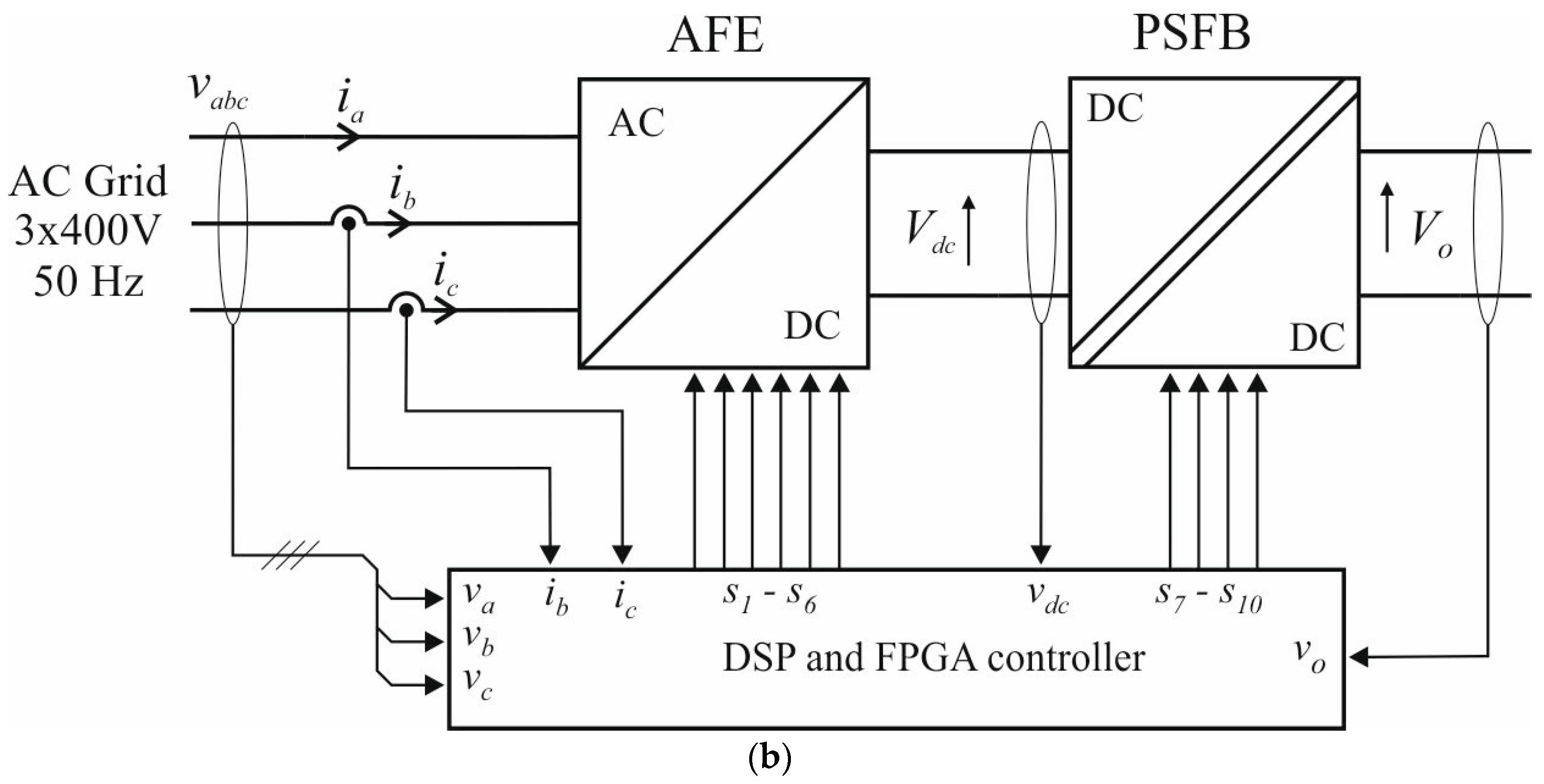
3.1. Laboratory Setup

The charger setup is powered by three modules of 5001 iX(C1) grid simulator connected in a star configuration. ITECH 8018B-800-75 is used as an active load to simulate a resistor of an accurately tunable resistance value. The device also allows programming sudden resistance changes, which is used in dynamic tests of the control system. As for measurements, the WT1800 power analyzer is connected at the input of AFE, between AFE and PSFB, and at the output of PSFB. This way, efficiencies of both power conversion stages can be measured separately. The connection scheme is shown in Figure 10a. Figure 10b, on the other hand, shows a photograph of the AFE connected with the PSFB. It should be noted that twisted wires go from AFE to the power analyzer and return to PSFB. AFE consists of a single power board with three external inductors, while PSFB is composed of a planar transformer, primary-side power board, and a separate secondary-side power board. Figure 10c presents the entire laboratory setup.

3.2. Laboratory Tests

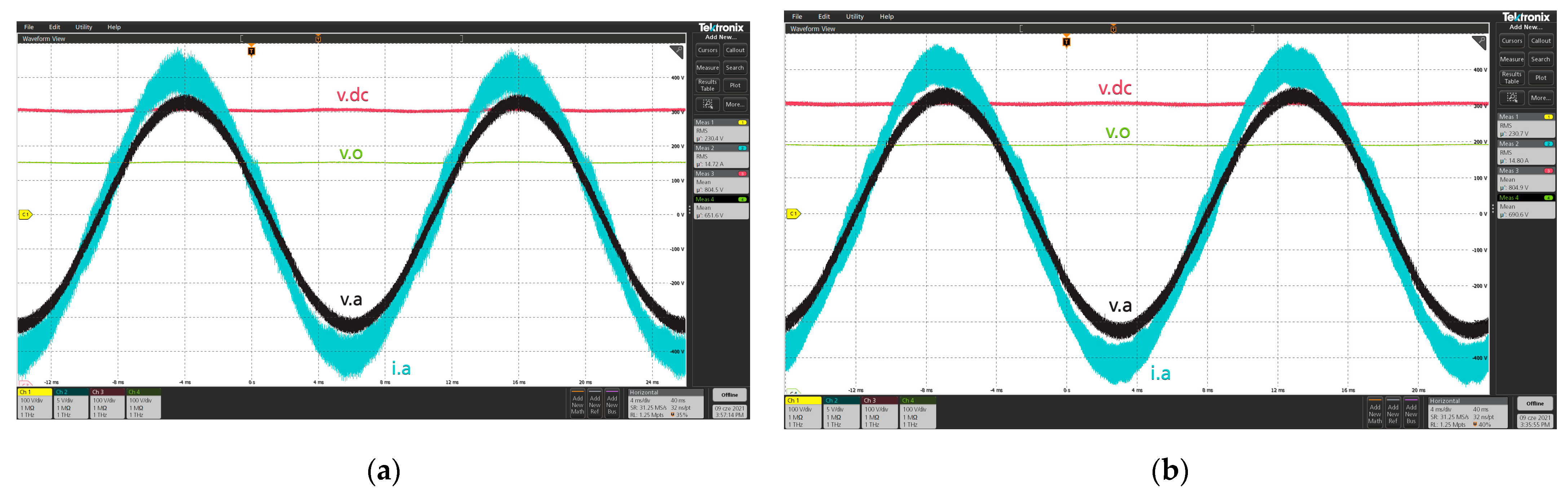
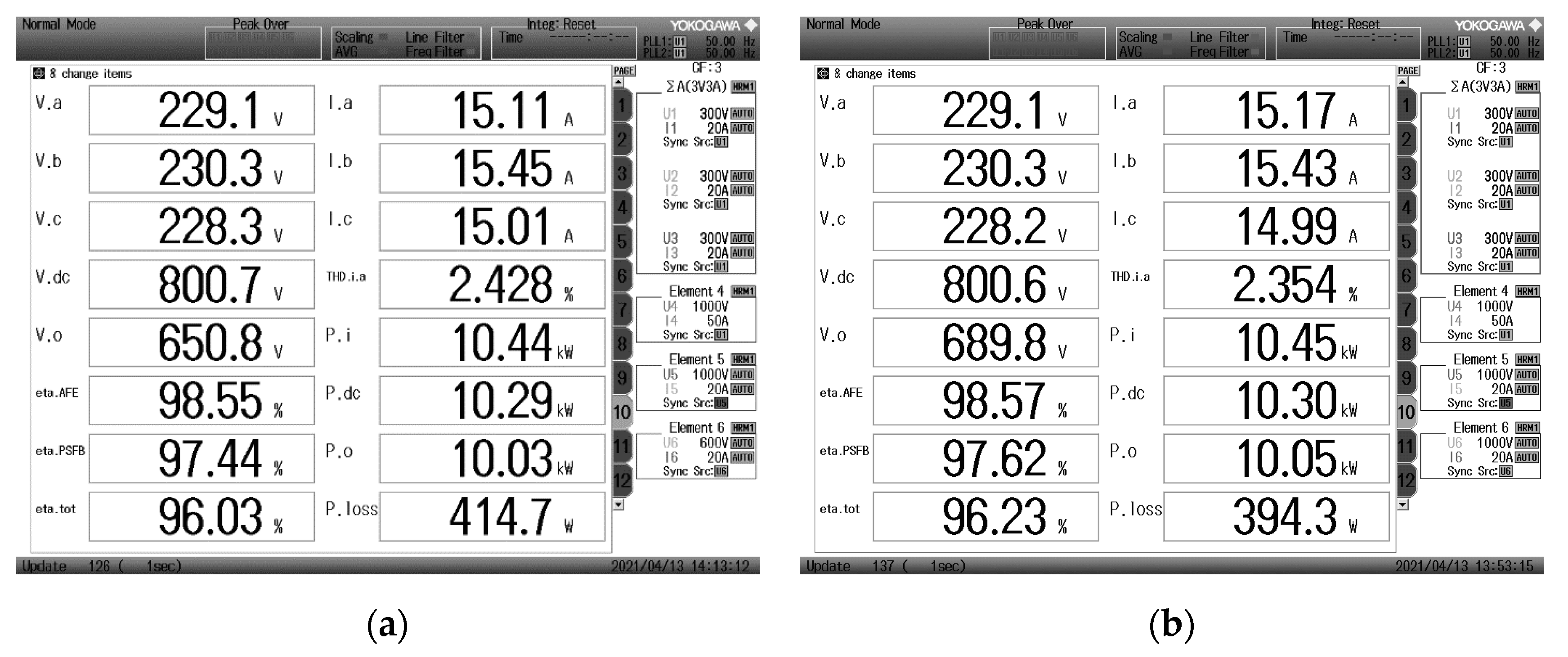
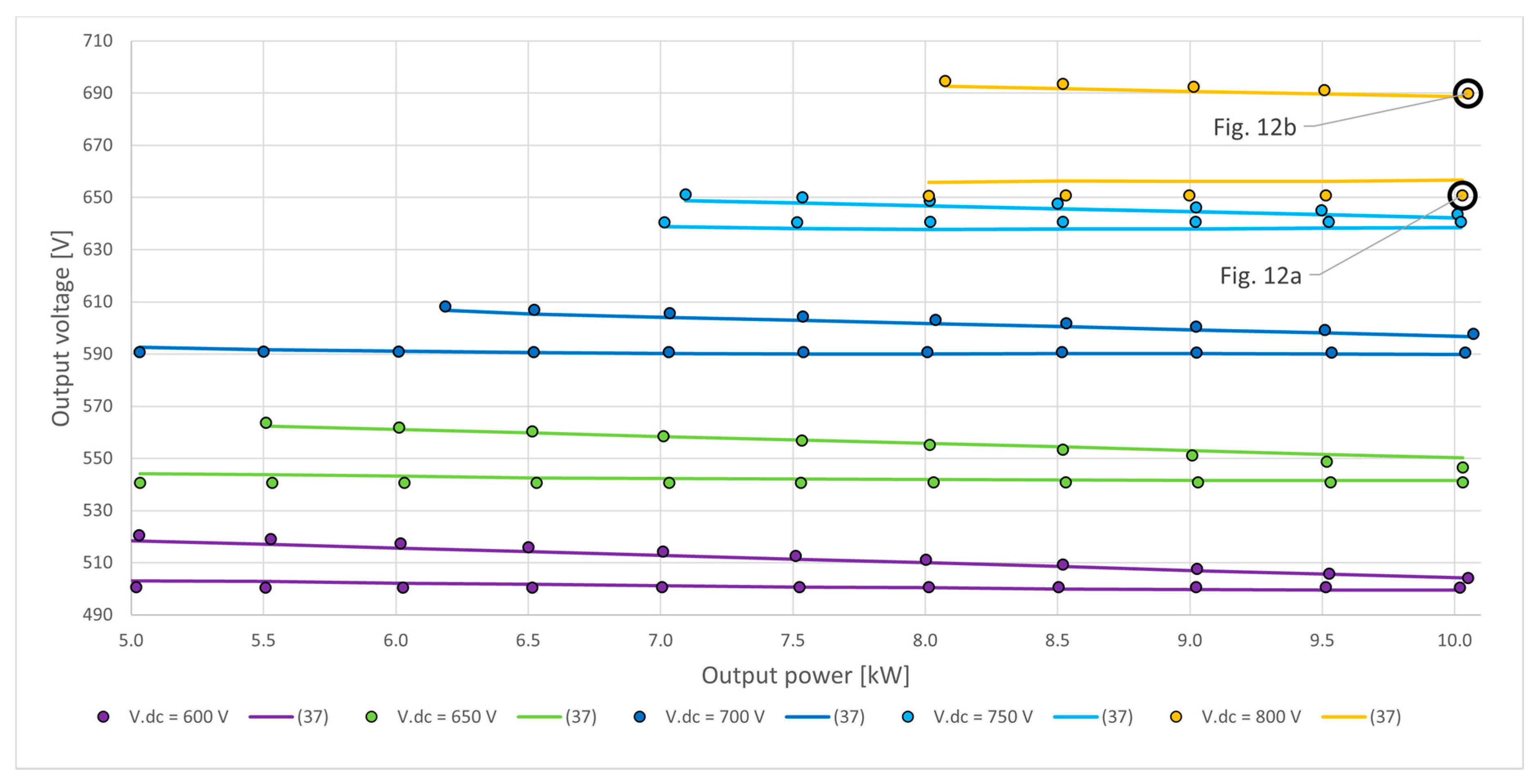
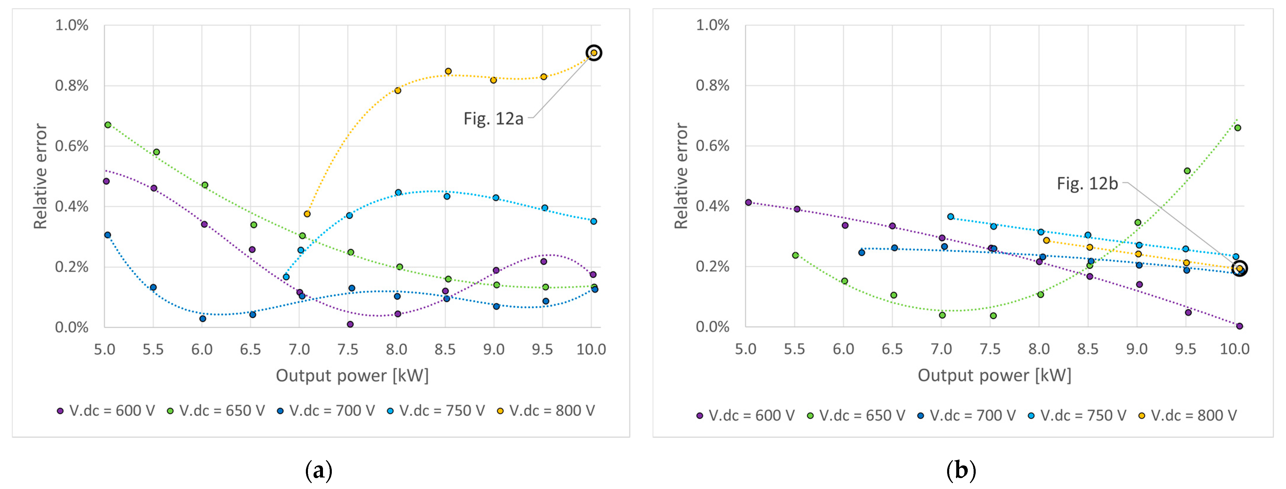
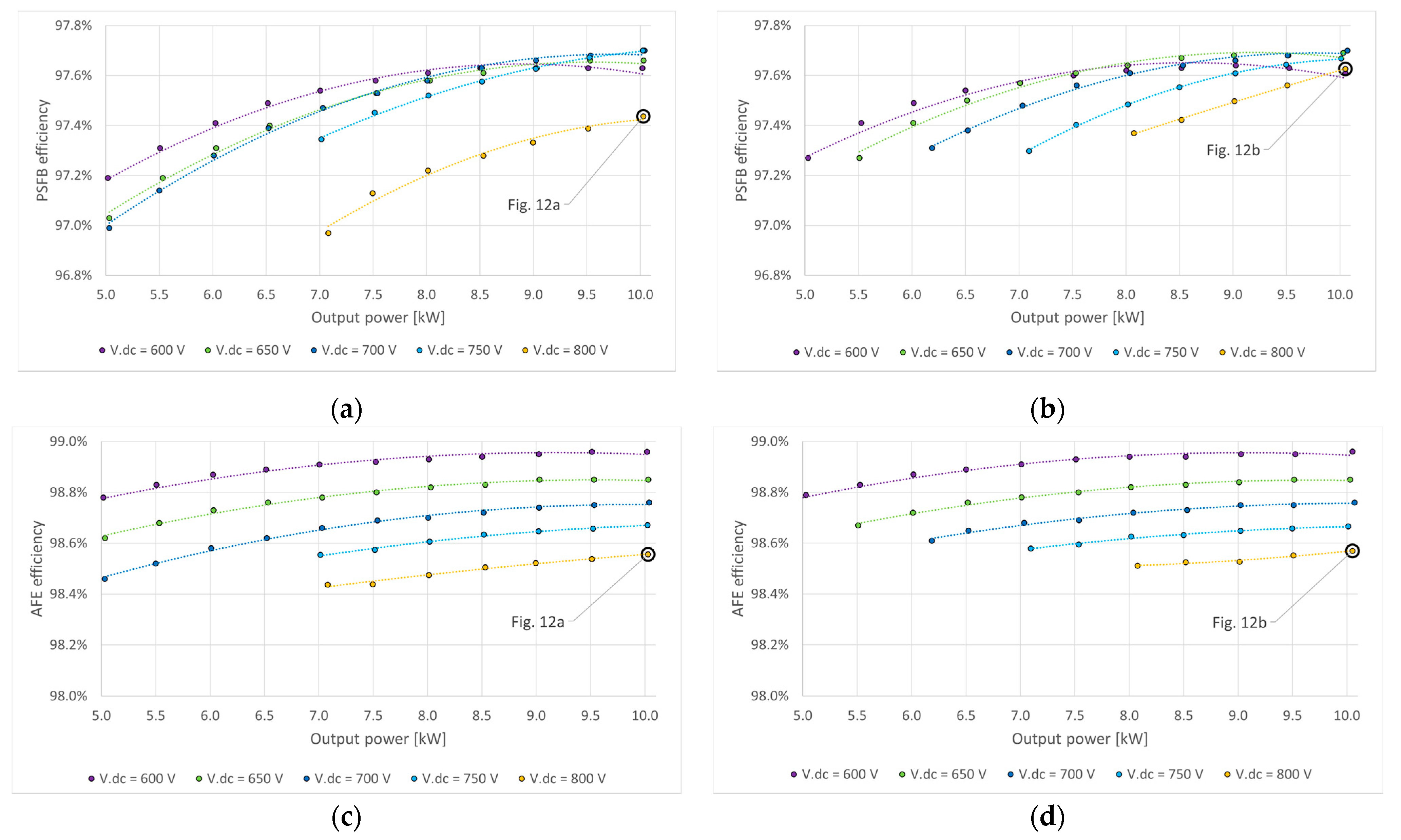
Steady-State Operation

First, the charger was thoroughly tested in steady-state conditions at several DC-link voltage and output voltage levels as well as at a couple of power levels. Oscilloscope results from two points of operation are shown in Figure 11a,b. These waveforms prove proper PLL and current control operation of the AFE stage since AC current is in phase with AC voltage. Additionally, both the DC-link voltage vdc and output voltage vo are kept constant with the exception of some acceptable amount of ripple.
Figure 12a,b shows power analyzer results for two operating points. Based on the values of Vdc read from these screenshots, as well as from screenshots for all other operating points, Vo values were calculated with the Formula (37) and compared with Vo values obtained from the power analyzer. Results were juxtaposed in the following figures. Figure 13 shows two modes in which the steady-state experiments were conducted: fixed output voltage mode and maximum output voltage mode. In the first one, the output voltage was fixed at a particular value, which meant that the device was operated with closed-loop voltage control, and the value of φ was varied at levels above zero. In the second mode, the PSFB was operated in the open loop with phase shift ratio φ equal to zero to obtain the highest possible value of output voltage Vo (see Figure 5c). It should be noted that the dots in Figure 13 correspond to the results obtained from the laboratory experiments, while the lines are values calculated using (37). Due to the parasitic resistances of the laboratory setup, the fitting cannot be ideal; however, the results predicted by the model are very close to the measured ones.
The absolute error values are shown in Figure 14. Figure 14a,b demonstrates the high accuracy of the developed model, with absolute error values kept firmly below 1%. High nonlinearity is shown, which results from the complexities of this topology, as shown mathematically in the formula set in Appendix A.
The non-zero error values in Figure 14 result from the omission of the second-order parasitic components of the laboratory prototype; however, the accuracy is deemed high enough. Aside from proving the correctness of the Formula (37), which includes all first-order design parameters, the efficiency of both stages was also measured at every operating point and in both measurement modes. Regarding the PSFB, from Figure 15a,b it can be inferred that for constant Vdc and Po values, the higher is Vo, the lower are the losses. This conclusion is in line with the analytical results shown in Figure 8. On the other hand, the efficiency of the AFE in these two modes remains unchanged.

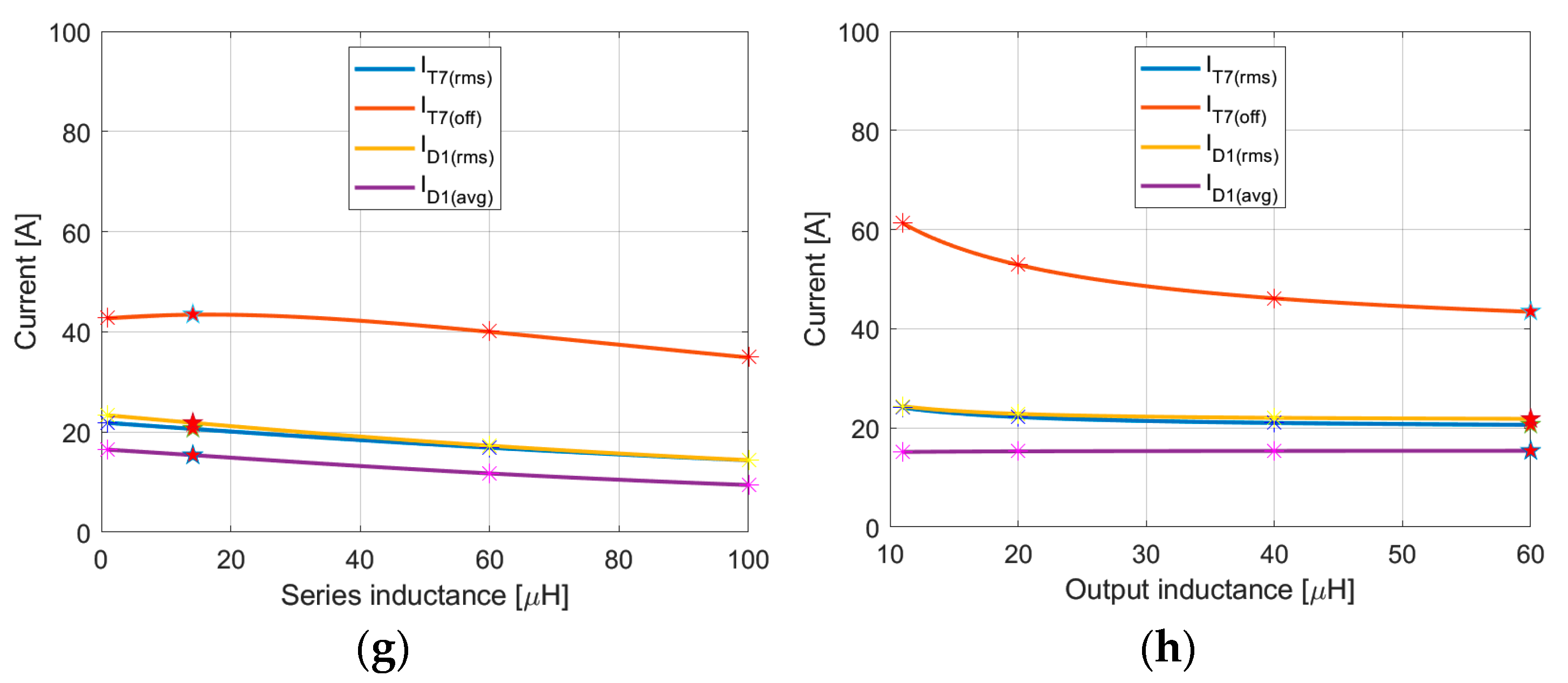
3.3. The Design Procedure

Having confirmed the accuracy of the developed expressions using simulations and laboratory experiments, it is possible to create a design procedure based on this analytical model. The proposed process makes use of MATLAB environment and the Symbolic Math Toolbox for dealing with the complex formulas. The first and most important step is to import the Formulas (1)–(32), (37)–(53), and (A1)–(A33) into MATLAB. Using the Symbolic Math Toolbox parameters can be automatically substituted for other parameters and formulas can be solved for any parameter. Therefore, the Formula (37), which is of the form:
V o = f ( V d c , R o , φ , f s , n , L m , L l , L o )
can be automatically converted by MATLAB into the form that includes the output power Po by substituting Ro with Vo2/Po:
V o = f ( V d c , P o , φ , f s , n , L m , L l , L o )
The only step missing at this point is to automatically solve (55) for the phase shift ratio φ and obtain:
φ = f ( V d c , P o , V o , f s , n , L m , L l , L o )
Please note that the automatic conversions eliminate the possibility of a human error, which exists only at the stage of implementing the Formulas (1)–(32), (37)–(53), and (A1)–(A33). Having the full set of formulas, the following design procedure, as shown in Figure 16, can be conducted. A single set of application requirements data is introduced. This set consists of electrical specification and thermal specification. The electrical part defines the desired DC-link voltage Vdc, output voltage Vo, output power Po, and maximum allowable ripple factor RFmax of the output inductor current. The thermal part, on the other hand, provides the requirements regarding the operating ambient temperature Ta, and maximum allowable junction temperatures of the transistors (TjT(max)) and the diodes (TjD(max)).
To satisfy all of these application requirements, multiple design variants must be checked for viability and the most optimal one must be selected. Switching frequency fs, turns ratio n, magnetizing inductance Lm, series inductance Ll, and output inductance Lo can be therefore provided in array forms with several values of each parameter in its particular array. The same is the case with the heatsink and the semiconductor database. As a result, the entire procedure is repeated as many times as there are unique combinations of each value of fs, n, Lm, Ll, Lo, and each model of the heatsink, transistor, and diode. Throughout each iteration, first, φ is calculated using (55) and it is checked whether its value lies between 0 and 0.5. If it does not, then this iteration is stopped, and the next set of design parameters is loaded, restarting from (55). If φ is located in the range (0; 0.5), the phase shift ratio is used for further calculations using Formulas (1)–(19), after which the value of RF is obtained based on (20) and compared with RFmax from the application requirements. If RF is higher than RFmax, the iteration is cancelled, and the next parameter set is selected. If RF is low enough, calculations (21)–(32) and (38)–(47) are conducted and the following values are obtained: IT7(rms), IT7(off), ID1(rms), ID1(avg), but also VLm(I) and VLm(III). Using values of voltages VLm(I), VLm(III), and also n, the diode database is restricted to only those diodes with a high enough breakdown voltage value. Formulas for this can be observed in the diode waveforms in Figure 6b. Similar exclusion of the lower-voltage transistors is conducted based on the value of Vdc. For the remaining diodes, the following values are imported from the database: threshold voltage VD1(th), dynamic resistance rD1, and junction-case thermal resistance Rth,j-c(D). For the remaining transistors, the following values are obtained: on-state resistance rT7, switch-off energy Eoff_T7 (calculated using Vdc and IT7(off)), and junction-case thermal resistance Rth,j-c(T). Afterwards, calculations using Formulas (48)–(51) are conducted to obtain losses in each transistor and diode, as well as the total losses. Using the thermal specification from the application requirements, a component from the heatsink database, and the results obtained so far, calculations (52) and (53) are realised. If any of the maximum junction temperatures are exceeded (TjT higher than TjT(max) or TjD higher than TjD(max)), the iteration stops and the next set of design parameters is considered, starting from (56). If the calculated temperatures are low enough, this particular design set is added to a viable design set and placed on a characteristic, such as these shown in Figure 17. After all defined sets are analyzed and qualified as either viable or not viable, the characteristics are completed and a design is selected according to the desired priority, e.g., lowest semiconductor losses, smallest volume, or lowest cost. Such results are provided in Table 5, where the application requirements used are provided in the table caption and the results of the automatic selection are provided in the table body. For each power level, three optimization directions were taken, and the appropriate fields contain underlined values to show this. For example, for the 20-kW PSFB with the lowest cost in mind, one should opt for C3M0032120J1 SiC transistors, STPSC20H12C SiC diodes, and LA V 6 150 12 heatsink. In that case, the recommended series inductance Ll is 25 μH. This is almost the maximum inductance value that will allow obtaining Vo = 650 V for the given conditions, while minimizing the total losses (see Figure 8d). Of course, a more developed semiconductor and heatsink database could provide results that are even better than these. By comparing the results from Table 5 and Figure 17 it can be seen that the optimal designs are placed in the lower left corners of the characteristics.

4. Discussion

The results confirm correctness of the developed analytical model, both by simulation and by laboratory experiments. The automated design procedure based on this model provides the much-needed accuracy with regard to the design of high-power high-voltage converters based on the PSFB topology. This is a great alternative to conducting simulations at multiple parameter values and using many different semiconductor and heatsink models. Aside from a much higher speed of calculation of hundreds of variants, the MATLAB-based approach allows one to keep track of any desired value in any considered variant. This enables not only the selection of the lowest losses, or the smallest heatsink, but also the optimization of the design with regard to any other factor, such as cost or junction temperature. The developed design methodology can find application in all fields where a high-power, high-voltage, isolated topology such as PSFB can be used. Furthermore, not only AC–DC applications such as EV chargers can benefit from it—it can also be applied in DC–AC converters such as solar inverters with a DC–DC stage. In these cases, it is enough to keep in mind that parameter Vo, as referred to in this work, becomes the DC-link voltage, and parameter Vdc becomes the output voltage of the photovoltaic array. Proper definition of the transformer turns ratio should also be assumed, as shown in Figure 1b. In future work, magnetic design procedure could be incorporated into this method, including losses in those components. This would enable prediction of total volume of the converter in the same automated fashion. Nevertheless, the main point is that without an accurate and verified formula such as (37), this sort of optimization of converters based on PSFB topology would not be possible.

Author Contributions

Conceptualization, K.W.; methodology, K.W.; software, M.S.; validation, K.W., P.G. and M.S.; formal analysis, K.W.; investigation, K.W.; resources, P.G.; data curation, M.S. and K.W.; writing—original draft preparation, K.W.; writing—review and editing, R.B.; visualization, P.G.; supervision, P.G.; project administration, P.G.; funding acquisition, P.G. All authors have read and agreed to the published version of the manuscript.

Funding

This research was supported and the APC was funded by The National Centre for Research and Development (NCBR), grant number MAZOWSZE/0111/19.

Conflicts of Interest

The authors declare no conflict of interest. The funders had no role in the design of the study; in the collection, analyses, or interpretation of data; in the writing of the manuscript, or in the decision to publish the results.

Appendix A

The expression (37) consists of one of the main design parameters, Vdc, and nine other parameters that are defined here: m, p, c, d, e, h, g, b, and z. As will be shown in the formulas below, all these parameters consist only of the remaining design parameters: Ro, φ, fs, n, Lm, Ll, and Lo. As a result, the expression (37) is shown to consist exclusively of the main set of design parameters. First, let us define two auxiliary parameters: k1 and k2.
k 1 = 2 · L m · n
k 2 = R o f s
Based on (A1) and (A2), as well as on the design parameters, m1m5 can be obtained, which leads to a simple calculation of m.
m 1 = k 1 4 · n 4 · ( L o · ( L o + k 2 · ( φ · ( 2 · φ 3 ) + 1 ) ) + k 2 2 · φ 2 · ( φ · ( φ 1 ) + 1 4 ) )
m 2 = k 1 3 · n 3 · L o · ( 4 · L o · ( L o + k 2 · ( φ · ( φ 3 ) + 5 4 ) ) + 2 · k 2 2 · φ · ( φ · ( 1 φ ) 1 4 ) )
m 3 = k 1 2 · n 2 · L o 2 · ( 4 · L o · ( L o + 2 · k 2 · ( 1 3 2 · φ ) ) + 3 · k 2 2 · ( φ · ( φ 2 3 ) + 1 12 ) )
m 4 = k 1 · n · L o 3 · k 2 · ( 4 · L o + k 2 · ( 1 2 · φ ) )
m 5 = L o 4 · k 2 2
m = ( m 1 + m 2 + m 3 + m 4 + m 5 ) · L l 4
Using (A1)–(A2), a couple of design parameters and auxiliary parameters, p1p4, p, is calculated in a straightforward manner.
p 1 = k 1 4 · n 2 · L o · ( L o · ( 2 · L o + k 2 · ( 2 · φ · ( φ 3 ) + 5 2 ) ) k 2 2 · φ · ( φ · ( φ 1 ) + 1 4 ) )
p 2 = k 1 3 · n · L o 2 · ( 4 · L o · ( L o + k 2 · ( 2 3 · φ ) ) + k 2 2 · ( φ · ( 3 · φ 2 ) + 1 4 ) )
p 3 = 3 · k 1 2 · L o 3 · k 2 · ( 2 · L o + k 2 · ( 1 2 φ ) )
p 4 = k 1 · 2 · L o 4 · k 2 2 n
p = ( p 1 + p 2 + p 3 + p 4 ) · L l 3
Parameter c can be obtained using three auxiliary parameters, c1c3, the design parameters, and (A1)–(A2).
c 1 = k 1 4 · L o 2 · ( L o · ( L o + k 2 · ( 2 3 · φ ) ) + 1 2 · k 2 2 · ( φ · ( 3 2 · φ 1 ) + 1 8 ) )
c 2 = 3 · k 1 3 · L o 3 · k 2 · L o + 1 2 · k 2 · ( 1 2 φ ) n
c 3 = k 1 2 · 3 2 · L o 4 · k 2 2 n 2
c = ( c 1 + c 2 + c 3 ) · L l 2
Parameter d, required for the Formula (37), can be calculated based on two auxiliary parameters, d1 and d2, the design parameters, and (A1)–(A2).
d 1 = k 1 4 · L o 3 · k 2 · L o + 1 2 · k 2 · ( 1 2 φ ) 2 · n 2
d 2 = k 1 3 · L o 4 · k 2 2 2 · n 3
d = ( d 1 + d 2 ) · L l
The final parameter inside of the square root of (37) is e, which can be calculated using two design parameters, (A1), and (A2).
e = k 1 4 · L o 4 · k 2 2 16 · n 4
The first parameter outside of the square root of the Formula (37) is h, which can be obtained using auxiliary parameters h1h3, the design parameters, and (A1)–(A2).
h 1 = k 1 2 · n 2 · ( L o + k 2 · φ · ( φ 1 2 ) )
h 2 = k 1 · n · L o · ( 2 · L o + k 2 · ( 1 2 φ ) )
h 3 = L o 2 · k 2
h = ( h 1 + h 2 + h 3 ) · L l 2
To obtain g, the penultimate parameter in the numerator of the Formula (37), the use of design parameters (A1), (A2) and two auxiliary parameters g1 and g2 is required.
g 1 = k 1 2 · L o · ( L o + 1 2 · k 2 · ( 1 2 φ ) )
g 2 = k 1 · L o 2 · k 2 n
g = ( g 1 + g 2 ) · L l
Parameter b is the final one in the numerator of (37). It can be obtained simply by using (A1), (A2), and two of the design parameters.
b = k 1 2 · L o 2 · k 2 4 · n 2
Parameter z belongs in the denominator of the Formula (37) and can be obtained based on (A1) and the design parameters, using auxiliary parameters z1z3.
z 1 = L l · k 1 · n 2
z 2 = L l · L o
z 3 = k 1 · L o 2 · n
z = ( z 1 + z 2 + z 3 ) · 4 · L l 2 · k 1 · n 2

References

  1. Burkart, R.M.; Kolar, J.W. Advanced Modeling and Multi-Objective Optimization/Evaluation of SiC Converter Systems. In Proceedings of the Tutorial at the 3rd IEEE Workshop on Wide Bandgap Power Devices and Applications (WiPDA 2015), Blacksburg, VA, USA, 2–5 November 2015. [Google Scholar]
  2. Sabate, J.A.; Vlatkovic, V.; Ridley, R.B.; Lee, F.C.; Cho, B.H. Design considerations for high-voltage high-power full-bridge zero-voltage-switched PWM converter. In Proceedings of the Applied Power Electronics Conference and Exposition (APEC), Los Angeles, CA, USA, 11–16 March 1990; pp. 275–284. [Google Scholar] [CrossRef]
  3. Kazimierczuk, M.K. Pulse-Width Modulated DC–DC Power Converters, 2nd ed.; John Wiley & Sons, Ltd.: Chichester, UK, 2016; pp. 330–361. [Google Scholar]
  4. Whitaker, B.; Barkley, A.; Cole, Z.; Passmore, B.; Martin, D.; McNutt, T.R.; Lostetter, A.B.; Lee, J.S.; Shiozaki, K. A High-Density, High-Efficiency, Isolated On-Board Vehicle Battery Charger Utilizing Silicon Carbide Power Devices. IEEE Trans. Power Electron. 2014, 29, 2606–2617. [Google Scholar] [CrossRef]
  5. Kanamarlapudi, V.R.K.; Wang, B.; So, P.L.; Wang, Z. Analysis, Design, and Implementation of an APWM ZVZCS Full-Bridge DC–DC Converter for Battery Charging in Electric Vehicles. IEEE Trans. Power Electron. 2017, 32, 6145–6160. [Google Scholar] [CrossRef]
  6. Ravyts, S.; Vecchia, M.D.; Zwysen, J.; Van den Broeck, G.; Driesen, J. Study on a cascaded DC-DC converter for use in building-integrated photovoltaics. In Proceedings of the IEEE Texas Power and Energy Conference (TPEC), College Station, TX, USA, 8–9 February 2018; pp. 1–6. [Google Scholar] [CrossRef]
  7. Piasecki, S.; Jasinski, M.; Wrona, G.; Chmielak, W. Robust control of grid connected AC-DC converter for distributed generation. In Proceedings of the IECON 2012—38th Annual Conference on IEEE Industrial Electronics Society, Montreal, QC, Canada, 25–28 October 2012; pp. 5840–5845. [Google Scholar] [CrossRef]
  8. Rodríguez, P.; Teodorescu, R.; Candela, I.; Timbus, A.V.; Liserre, M.; Blaabjerg, F. New positive-sequence voltage detector for grid synchronization of power converters under faulty grid conditions. In Proceedings of the 37th IEEE Power Electronics Specialists Conference, Jeju, Korea, 18–22 June 2006; pp. 1–7. [Google Scholar] [CrossRef]
  9. Barlik, R.; Grzejszczak, P.; Leszczyński, B.; Szymczak, M. Investigation of a high-efficiency and high-frequency 10-kW/800-V three-phase PWM converter with direct power factor control. Int. J. Electron. Telecommun. 2019, 65, 619–624. [Google Scholar] [CrossRef]
  10. Hassanzadeh, N.; Yazdani, F.; Haghbin, S.; Thiringer, T. Design of a 50 kW Phase-Shifted Full-Bridge Converter Used for Fast Charging Applications. In Proceedings of the IEEE Vehicle Power and Propulsion Conference (VPPC), Belfort, France, 11–14 December 2017; pp. 1–5. [Google Scholar] [CrossRef]
  11. Escudero, M.; Kutschak, M.-A.; Meneses, D.; Rodriguez, N.; Morales, D.P. A Practical Approach to the Design of a Highly Efficient PSFB DC-DC Converter for Server Applications. Energies 2019, 12, 3723. [Google Scholar] [CrossRef] [Green Version]
  12. Kim, J.-M.; Lee, J.; Ryu, K.; Won, C.-Y. Power Device Temperature-Balancing Control Method for a Phase-Shift Full-Bridge Converter. Energies 2020, 13, 1623. [Google Scholar] [CrossRef] [Green Version]
  13. Zhao, L.; Li, H.; Liu, Y.; Li, Z. High Efficiency Variable-Frequency Full-Bridge Converter with a Load Adaptive Control Method Based on the Loss Model. Energies 2015, 8, 2647–2673. [Google Scholar] [CrossRef] [Green Version]
  14. Lai, Y.; Su, Z.; Chang, Y. Novel Phase-Shift Control Technique for Full-Bridge Converter to Reduce Thermal Imbalance under Light-Load Condition. IEEE Trans. Ind. Appl. 2015, 51, 1651–1659. [Google Scholar] [CrossRef]
  15. Chen, B.; Lai, Y. Switching Control Technique of Phase-Shift-Controlled Full-Bridge Converter to Improve Efficiency under Light-Load and Standby Conditions Without Additional Auxiliary Components. IEEE Trans. Power Electron. 2010, 25, 1001–1012. [Google Scholar] [CrossRef]
  16. Lee, W.; Kim, C.; Moon, G.; Han, S. A New Phase-Shifted Full-Bridge Converter with Voltage-Doubler-Type Rectifier for High-Efficiency PDP Sustaining Power Module. IEEE Trans. Ind. Electron. 2008, 55, 2450–2458. [Google Scholar] [CrossRef]
  17. Shu, L.; Chen, W.; Ma, D.; Ning, G. Analysis of Strategy for Achieving Zero-Current Switching in Full-Bridge Converters. IEEE Trans. Ind. Electron. 2018, 65, 5509–5517. [Google Scholar] [CrossRef]
  18. Shih, L.; Liu, Y.; Chiu, H. A Novel Hybrid Mode Control for a Phase-Shift Full-Bridge Converter Featuring High Efficiency over a Full-Load Range. IEEE Trans. Power Electron. 2019, 34, 2794–2804. [Google Scholar] [CrossRef]
  19. Pástor, M.; Dudrik, J.; Vitkovská, A. Soft-Switching DC-DC Converter with SiC Full-Bridge Rectifier. In Proceedings of the International Conference on Electrical Drives & Power Electronics (EDPE), The High Tatras, Slovakia, 24–26 September 2019; pp. 347–352. [Google Scholar] [CrossRef]
  20. Bouvier, Y.E.; Serrano, D.; Borović, U.; Moreno, G.; Vasić, M.; Oliver, J.A.; Alou, P.; Cobos, J.A.; Carmena, J. ZVS Auxiliary Circuit for a 10 kW Unregulated LLC Full-Bridge Operating at Resonant Frequency for Aircraft Application. Energies 2019, 12, 1850. [Google Scholar] [CrossRef] [Green Version]
  21. Xiaofeng, X. Small-signal model for current mode control full-bridge phase-shifted ZVS converter. In Proceedings of the Third International Power Electronics and Motion Control Conference (IPEMC), Beijing, China, 15–18 August 2000; pp. 514–518. [Google Scholar] [CrossRef]
  22. Schutten, M.J.; Torrey, D.A. Improved small-signal analysis for the phase-shifted PWM power converter. IEEE Trans. Power Electron. 2003, 18, 659–669. [Google Scholar] [CrossRef]
  23. Loh, C.K.R.M. Phase Shifted Bridge Converter for a High Voltage Application. Ph.D. Thesis, The University of Edinburgh, Edinburgh, Scotland, December 2003. [Google Scholar]
  24. Li, P.; Wang, Q.; Zhao, Y.; Lu, S. Power conversion efficiency calculation models for electric vehicle fast charger system. In Proceedings of the 13th IEEE Conference on Industrial Electronics and Applications (ICIEA), Wuhan, China, 31 May–2 June 2018; pp. 316–321. [Google Scholar] [CrossRef]
  25. Awwad, A.E.; Badawi, N.; Dieckerhoff, S. Efficiency analysis of a high frequency PS-ZVS isolated unidirectional full-bridge DC-DC converter based on SiC MOSFETs. In Proceedings of the 18th European Conference on Power Electronics and Applications (EPE’16 ECCE Europe), Karlsruhe, Germany, 5–9 September 2016; pp. 1–10. [Google Scholar] [CrossRef]
  26. Petreus, D.; Etz, R.; Patarau, T.; Ciocan, I. Comprehensive Analysis of a High-Power Density Phase-Shift Full Bridge Converter Highlighting the Effects of the Parasitic Capacitances. Energies 2020, 13, 1439. [Google Scholar] [CrossRef] [Green Version]
  27. Kasper, M.; Burkart, R.M.; Deboy, G.; Kolar, J.W. ZVS of Power MOSFETs Revisited. IEEE Trans. Power Electron. 2016, 31, 8063–8067. [Google Scholar] [CrossRef]
  28. Roig, J.; Gomez, G.; Bauwens, F.; Vlachakis, B.; Rogina, M.R.; Rodriguez, A.; Lamar, D.G. High-accuracy modelling of ZVS energy loss in advanced power transistors. In Proceedings of the 2018 IEEE Applied Power Electronics Conference and Exposition (APEC), San Antonio, TX, USA, 4–8 March 2018; pp. 263–269. [Google Scholar] [CrossRef] [Green Version]
  29. Ayyanar, R.; Mohan, N. Novel soft-switching DC-DC converter with full ZVS-range and reduced filter requirement. I. Regulated-output applications. IEEE Trans. Power Electron. 2001, 16, 184–192. [Google Scholar] [CrossRef]
  30. Szymczak, M.; Grzejszczak, P.; Barlik, R. Control strategies for isolated high-frequency modular DC/DC converter implemented in programmable logic array. In Proceedings of the Progress in Applied Electrical Engineering Conference, Koscielisko, Poland, 18–22 June 2018. [Google Scholar] [CrossRef]
  31. Barlik, R.; Grzejszczak, P.; Zdanowski, M. Determination of the Basic parameters of the high-frequency planar transformer. Prz. Elektrotech. 2016, 92, 71–78. [Google Scholar] [CrossRef] [Green Version]
Figure 1. Sample applications of the AFE + PSFB isolated grid-connected AC–DC converter: (a) EV charger; (b) PV Inverter.
Energies 14 05380 g001
Figure 2. Verification process of the analytical model.
Energies 14 05380 g002
Figure 3. Schemes: (a) detailed, showing components; (b) generalized, with control and measurement signals.
Energies 14 05380 g003aEnergies 14 05380 g003b
Figure 4. Analysis of PSFB operation: (a) independent states; (b) vital waveforms.
Energies 14 05380 g004
Figure 5. Output voltage calculation as a function of design parameters. Blue lines show the results according to Formula (37), PLECS simulation results for various parameters are in red, while results for selected parameters are symbolized by stars. The design parameters are: (a) Vdc; (b) Ro; (c) φ; (d) fs; (e) n; (f) Lm; (g) Ll; (h) Lo.
Energies 14 05380 g005
Figure 6. Analysis of PSFB operation continued: (a) independent states IV and V; (b) vital semiconductor waveforms.
Energies 14 05380 g006
Figure 7. Semiconductor current parameters—Formulas (41), (42), (46), (47) shown as lines vs. PLECS simulation results shown as symbols. Varied design parameter: (a) Vdc; (b) Ro; (c) φ; (d) fs; (e) n; (f) Lm; (g) Ll; (h) Lo.
Energies 14 05380 g007aEnergies 14 05380 g007b
Figure 8. Ploss(tot) (green) and φ (purple) at constant input and output parameters with Vdc = 800 V, Vo = 650 V / 690 V, Po = 10 kW. Varied design parameters are: (a) fs; (b) n; (c) Lm; (d) Ll; (e) Lo.
Energies 14 05380 g008
Figure 9. Control schemes of the charger stages: (a) AFE; (b) PSFB.
Energies 14 05380 g009
Figure 10. Laboratory setup: (a) connection scheme; (b) AFE (left side) with PSFB (right side); (c) entire experimental setup.
Energies 14 05380 g010
Figure 11. Waveforms of the converter with voltage of phase a (va) in black, current of phase a (ia) in light blue, DC-link voltage (vdc) in red, and output voltage (vo) in green at Vdc = 800 V, Po = 10 kW and: (a) Vo = 650 V; (b) Vo = 690 V.
Energies 14 05380 g011
Figure 12. Power analyzer measurements of the converter at Vdc = 800 V, Po = 10 kW and: (a) Vo = 650 V; (b) Vo = 690 V.
Energies 14 05380 g012
Figure 13. Output voltage as a function of output power in both examined modes—the fixed and the maximum output voltage mode. The symbols represent the experimental results, and the lines are obtained using Formula (37).
Energies 14 05380 g013
Figure 14. Relative error of Formula (37) in both examined modes: (a) fixed output voltage; (b) maximum output voltage.
Energies 14 05380 g014
Figure 15. Efficiency characteristics of both stages in both modes: (a) PSFB in fixed output voltage mode; (b) PSFB in maximum output voltage mode; (c) AFE in fixed output voltage mode; (d) AFE in maximum output voltage mode.
Energies 14 05380 g015
Figure 16. Design optimization approach for a PSFB-based converter.
Energies 14 05380 g016
Figure 17. Sets of automatically generated designs using the developed analytical model and databases of various types of transistors, diodes, and heatsinks. The application requirements are Vdc = 800 V, Vo = 650 V, RFmax = 1, Ta = 25 °C, TjT(max) = 150 °C, TjD(max) = 150 °C, Po = 10 kW: (a) losses vs. volume; (b) cost vs. volume; (c) cost vs. losses vs. volume; and Po = 20 kW: (d) losses vs. volume; (e) cost vs. volume; (f) cost vs. losses vs. volume.
Energies 14 05380 g017
Table 1. Example design parameters of an AC-DC charger.
ParameterSymbolValue
Input voltageVabc3 × 400 V, 50 Hz
DC-link voltageVdc800 V
Output voltageVo650 V
Output powerPo20 kW
Table 2. Default parameters selected for verification of the Formula (37) for the PSFB converter.
ParameterSymbolValue
DC-link voltageVdc800 V
Load resistanceRo21.125 Ω
Phase shift ratioφ1.43%
Switching frequencyfs25 kHz
Turns ration0.9
Magnetizing inductanceLm792 μH
Series inductanceLl14.15 μH
Output inductanceLo60 μH
Table 3. Control system parameters.
AFEPSFB
ControllerTMS320F28379D DSP10CL025 FPGA
Control frequency60 kHz25 kHz
Deadtime100 ns165 ns
ADC sampling12 bit, 120 kS/s12 bit, 250 kS/s
Resources usedCPU + CLA~20k LE
Table 4. Selected components of the AC–DC–DC charger prototype operating at Vabc = 3 × 400 V, Vdc = 600 V–800 V, Po = 5 kW–10 kW, fs = 25 kHz, fs(AFE) = 60 kHz.
ComponentParameterValueModel
PSFB transformern0.9Payton T10000AC-9-10
Lm792 μH
PSFB series inductorLl14.15 μH (incl. transf. leak.)Custom-made
PSFB output inductorLo60 μHCustom-made
AFE input inductorsLAC210 μHCustom-made
AFE transistorsT1–T6-C3M0021120K
PSFB transistorT7–T8-2 × SCTH100N120G2-AG
PSFB diodesD1–D4-2 × STPSC20H12CWL
Table 5. Results of operation of the automated component selection tool for PSFB. The following specification requirements are assumed: Vdc = 800 V, Vo = 650 V, RFmax = 1, Ta = 25 °C, TjT(max) = 150 °C, TjD(max) = 150 °C, Po = 10 kW / 20 kW.
PoVolume [dm3]CostPloss(tot) [W]T7–T10D1–D4Heatsinkfs [kHz]nLm [mH]Ll [μH]Lo [μH]
10 kW0.375$115169C3M0120100KSTPSC20H12CLAM 5 150 12200.91.536130
0.375$46676CAB011M12FM3C4D40120DLAM 5 150 12200.91.536130
0.125$18392C3M0032120J1C4D15120HLAM 5 50 12200.91.536130
20 kW0.688$193382C3M0032120J1STPSC20H12CLA V 6 150 12200.91.525130
0.688$495211CAB011M12FM3C4D40120DLA V 6 150 12200.91.525130
0.459$252299C3M0032120J1C4D15120HLA 6 100 12200.91.525130
Publisher’s Note: MDPI stays neutral with regard to jurisdictional claims in published maps and institutional affiliations.

